

Page 1

Intel740™ Graphics Accelerator
Design Guide
August 1998
Order Number: 290619-003
Page 2

Information in this document is provided in connection with Intel products. No license, express or implied, by estoppel or otherwise, to any intellectual
property rights is granted by this document. Except as provided in Intel's Terms and Conditions of Sale for such products, Intel assumes no liability
whatsoever, and Intel disclaims any express or implied warranty, relating to sale and/or use of Intel products including liability or warranties relating to
fitness for a particular purpose, merchantability, or infringement of any patent, copyright or other intellectual property right. Intel products are not
intended for use in medical, life saving, or life sustaining applications.
Intel may make changes to specifications and product descriptions at any time, without notice.
Contact your local Intel sales office or your distributor to obtain the latest specifications and before placing your product order.
The Intel740™ graphics accelerator may contain design defects or errors known as errata which may cause the products to deviate from published
specifications.
2
I
C is a two-wire communications bus/protocol developed by Philips. SMBus is a subset of the I2C bus/protocol and was developed by Intel.
Implementations of the I
North American Philips Corporation.
Copies of documents which have an ordering number and are referenced in this document, or other Intel literature may be obtained by:
Copyright © Intel Corporation, 1998
*Third-party brands and names are the property of their respective owners.
Such errata are not covered by Intel’s warranty.
2
C bus/protocol or the SMBus bus/protocol may require licenses from various entities, including Philips Electronics N.V. and
calling 1-800-548-4725 or
by visiting Intel's website at http://www.intel.com.
Current characterized errata are available upon request.
Intel740™ Graphics Accelerator Design Guide
Page 3

Contents
1 Introduction................................................................................................................1-1
1.1 About This Design Guide..............................................................................1-1
1.2 References....................................................................................................1-2
2 Addin Card Design.....................................................................................................2-1
2.1 Introduction ...................................................................................................2-1
2.1.1 Design Features...............................................................................2-2
2.1.1.1 Intel740™ Graphics Accelerator.....................................2-2
2.1.2 BT829B - Video Decoder .................................................................2-3
2.1.2.1 BT869 - TV Encoder.......................................................2-3
2.1.3 Terminology .....................................................................................2-3
2.1.3.1 Power Sources ...............................................................2-3
2.1.3.2 Fences............................................................................2-4
2.1.3.3 Stitching..........................................................................2-4
2.2 Layout and Routing Guidelines.....................................................................2-5
2.2.1 Placement........................................................................................2-5
2.2.2 Board Description ............................................................................2-6
2.2.3 BGA Component..............................................................................2-8
2.2.3.1 Layout Requirements......................................................2-8
2.2.3.2 Ground Connections.......................................................2-9
2.2.3.3 Power Connections.........................................................2-9
2.2.3.4 Decoupling....................................................................2-10
2.2.3.5 General Signal Routing.................................................2-11
2.2.4 Voltage Regulator ..........................................................................2-11
2.2.5 Bt829 Video Decoder.....................................................................2-11
2.2.5.1 Ground Planes..............................................................2-12
2.2.5.2 Power Planes................................................................2-12
2.2.5.3 Passive Components and Signal Routing ....................2-12
2.2.6 Bt869 Video Encoder.....................................................................2-12
2.2.6.1 Ground Planes..............................................................2-12
2.2.6.2 Power Planes................................................................2-13
2.2.6.3 Passive Components and Signal Routing ....................2-13
2.2.6.4 AGP Layout and Routing Guidelines............................2-13
2.2.6.5 Intel740™ Graphics Accelerator Memory
Layout and Routing Guidelines.....................................2-14
2.2.6.6 Intel740™ Graphics Accelerator Memory
Configurations...............................................................2-17
2.2.6.7 TV Out Interface ...........................................................2-20
2.2.6.8 Analog Signals....................................................... .......2-20
2.2.7 UL and FCC Considerations..........................................................2-20
2.3 Addin Card Schematics ..............................................................................2-21
Intel740™ Graphics Accelerator Design Guide
iii
Page 4

3 3 Device AGP MotherBoard Design ....................... ....... ...... ...... ....... ...... ....... ............3-1
3.1 Introduction......... ....... ...... ....... ...... ....... ...... ....... ...... ...... ....... .........................3-1
3.1.1 Overview....................................... ....... ...... ...... ....... ...... ....... ...... ......3-1
3.1.2 About This Chapter..........................................................................3-2
3.1.3 Block Diagram .................................................................................3-2
3.1.4 Implementation Issues.....................................................................3-3
3.1.4.1 Disabling A Master Device .............................................3-3
3.1.4.2 Low Power Logic Implementation...................................3-4
3.1.4.3 GPO27# and GPO28# Signal Duration..........................3-5
3.1.5 State Diagrams................................................................................3-5
3.1.5.1 Signal Quality and Timing Issues ...................................3-6
3.1.5.2 Strobe Edge Quality Issues............................................3-7
3.1.5.3 Clock Issues ...................................................................3-7
3.1.6 Design Recommendations...............................................................3-9
3.1.6.1 Voltage Definitions..........................................................3-9
3.1.6.2 General Design Recommendation .................................3-9
3.2 3 Device AGP Motherboard Layout and Routing Guidelines........................3-9
3.2.1 BGA Quadrant Assignment ...........................................................3-10
3.2.2 Board Description ..........................................................................3-12
3.2.3 3-point AGP Design Guidelines.....................................................3-12
3.2.3.1 Layout and Routing ............................................ ...... ....3-12
3.2.3.2 Data and strobe definitions...........................................3-13
3.2.3.3 Assumptions for Board Design Guidelines...................3-14
3.2.3.4 Add-in Card guideline assumptions:.............................3-14
3.2.3.5 Motherboard Guideline Assumptions ...........................3-14
3.2.3.6 3-Load AGP Topology..................................................3-16
3.2.3.7 Overall Solution Space.................................................3-16
3.2.4 Intel740™ Graphics Accelerator Memory Layout and
Routing Guidelines ....................... ....... ...... ....................................3 -18
3.2.4.1 3 Device AGP Intel740™ Graphics Accelerator
Memory Configurations ................................................3-21
3.3 3 Device AGP Motherboard Reference Design Schematics ......................3-22
4 Thermal Considerations.............................................................................................4-1
5 Mechanical Information..............................................................................................5-1
5.1 Board Dimensions ........................................................................................5-1
5.2 Fan/Heatsink Hole Pattern............................................................................5-1
5.3 VMI Header Placement.............................. ....... ...... ...... ....... ...... ....... ...... ......5-2
5.4 50 Pin Video Connector................................................................................5-3
5.5 Bracket..........................................................................................................5-4
5.6 NLX Considerations................................... ....... ...... ...... ....... ...... ...................5-5
6 Third Party Vendors...................................................................................................6-1
6.1 Voltage Regulator.........................................................................................6-1
6.2 50 Pin Connector..........................................................................................6-1
6.3 Fan/Heatsink.................................................................................................6-1
6.4 Flash Components........................................................................................6-1
6.5 Video Encoders/Decode rs ...................................... ...... ....... .........................6-1
6.6 DVD Daughter Cards....................................................................................6-2
6.7 TV Tuner.......................................................................................................6-2
A Application Notes
B Reference Information
iv
Intel740™ Graphics Accelerator Design Guide
Page 5

Figures
2-1 Example of Power Plane Separation ("fencing")...........................................2-4
2-2 Example of Power Plane Stitching................................................................2-4
2-3 Major Signal Sections...................................................................................2-5
2-4 Example ATX Layout....................................................................................2-6
2-5 Four Layer Board Stack-up...........................................................................2-7
2-6 Metal Defined land dimensions.....................................................................2-8
2-7 BGA Trace....................................................................................................2-8
2-8 Dogbone Via Pattern.....................................................................................2-9
2-9 Suggested VCC Planes for the Intel740™ Graphics Accelerator...............2-10
2-10 Intel740™ Graphics Accelerator Decoupling..............................................2-10
2-11 Intel740™ Graphics Accelerator BGA Routing Example............................2-11
2-12 Layout Dimensions (MA[11:0])....................................................................2-15
2-13 Layout Dimensions (MD[63:0], DQM[7:0])..................................................2-15
2-14 Layout Dimensions (WEA#, SRASA#, SCASA#, CSA1#, CSB0#).............2-15
2-15 Layout Dimensions (WEB#, SRASB#, SCASB#, CSA0#)..........................2-16
2-16 Memory Layout Dimensions (TCLK0).........................................................2-16
2-17 Memory Layout Dimensions (TCLK1).........................................................2-16
2-18 Memory Layout Dimensions (RCLK and OCLK to RCLK)..........................2-17
2-19 2/4 MB Local Memory Connection (64-bit data path) .................................2-17
2-20 4/8 MB Local Memory Connection (64-bit data path) .................................2-18
2-21 8 MB Local Memory Connection (64-bit data path) ....................................2-19
2-22 Layout Dimensions, Digital TV Bus.............................................................2-20
2-23 512Kx32 and 256Kx32 Pinout Compatibility...............................................2-24
2-24 1M X 16 Pinout Compatibility.....................................................................2-24
3-1 Pentium
®
II Processor / Intel® 440BX AGPset/Intel 740 Graphics
Accelerator System Block Diagram ..............................................................3-3
3-2 The Schematic Diagram for GPO27#, PCIRST# (System Reset),
RESET#, ROMA16 Signals ..........................................................................3-4
3-3 The Schematic Diagram for the WEB#, SCASB#, SRASB#,
CS0B#, CS1B# and TEST............................................................................3-5
3-4 Intel740™ Graphics Controller (On Board Device) Remains in
Low Power Mode ..........................................................................................3-6
3-5 Intel740™ Graphics Controller (On Board Device) State Diagram...............3-6
3-6 Point-to-Point Topology ................................................................................3-8
3-7 Major Signal Sections.................................................................................3-10
3-8 Example ATX Placement for a UP Pentium
®
Intel
440BX AGPset / Intel 740 Graphics Accelerator Design ..................3-11
®
II Processor /
3-9 Four Layer Board Stack-up.........................................................................3-12
3-10 Point-to-Point Topology ..............................................................................3-15
3-11 3 Device Data Load Topology.....................................................................3-16
3-12 3 Device Strobe Load Topology..................................................................3-16
3-13 3 Device Data Load Topology (Solution 1 is Shown)..................................3-17
3-14 3 Device Strobe Load Topology (Solution 1 is shown) ...............................3-17
3-15 Clock Topology and Matching.....................................................................3-17
3-16 Layout Dimensions (MA[11:0])....................................................................3-19
3-17 Layout Dimensions (MD[63:0], DQM[7:0])..................................................3-19
3-18 Layout Dimensions (WEA#, SRASA#, SCASA#, CSA0#)..........................3-20
3-19 Memory Layout Dimensions (TCLK1).........................................................3-20
3-20 Memory Layout Dimensions (RCLK and OCLK to RCLK)..........................3-21
Intel740™ Graphics Accelerator Design Guide
v
Page 6

3-21 2/4 MB Local Memory Connection (64-bit data path) .................................3-21
3-22 512Kx32 and 256Kx32 Pinout Compatibility...............................................3-26
3-23 1M X 16 Pinout Compatibility.....................................................................3-26
5-1 Mounting Hole Locations (Fan/Heatsink Assembly).....................................5-1
5-2 VMI Header Placement........................ ...... ....... ...................................... ......5-2
5-3 DVD Daughter Card Dimensions (ATX and NLX)—Top Side ......................5-2
5-4 50 Pin Video Connector Schematic..............................................................5-3
5-5 Recommended Bracket Placement ..............................................................5-4
5-6 Recommended Bracket Cutout.....................................................................5-4
vi
Intel740™ Graphics Accelerator Design Guide
Page 7

Tables
2-1 Mix and Match Options For Intel740™ Graphics Accelerator Card..............2-2
2-2 Intel740™ Graphics Accelerator Power Supplies.........................................2-3
2-3 Bt829B GND and AGND Pins.....................................................................2-12
2-4 Bt829B VCC and AVCC Pins......................................................................2-12
2-5 Bt869 Digital and Analog Power Pins .........................................................2-13
2-6 AGP Signal Lengths....................................................................................2-13
2-7 Strobes and Corresponding Signal Groups ................................................2-13
2-8 Supported Memory Options (Other Memory Options Are
Not Supported)............................................................................................2-14
2-9 Memory Layout Restrictions (See Figure 2-12 and Figure 2-13)................2-14
2-10 Memory Layout Restrictions (See Figure 2-14 and Figure 2-15)................2-15
2-11 Memory Layout Restrictions (See Figure 2-16 and Figure 2-17)................2-16
2-12 TV Out/ROMA Trace Lengths (See Figure 2-22)........................................2-20
2-13 GPIO Functions ................................................... ...... ....... ..........................2-21
3-1 State of Signals to be Driven After System Reset but at Least
One Clock Prior to Asserting TEST ..............................................................3-4
3-2 Signal Duration of the GPO Signals from PIIX4............................................3-5
3-3 Data and Associated Strobe.......................................................................3-13
3-4 Data Signal and Strobe Guideline Assumptions.........................................3-14
3-5 Control and Clock Signal Guideline Assumptions.......................................3-14
3-6 Data signal and strobe requirements..........................................................3-14
3-7 Control Signal Line Length Requirements ..................................................3-15
3-8 Strobe and Data Segment Solution Space .................................................3-16
3-9 Clock Segment Solution Space ..................................................................3-18
3-10 Supported Memory Options (Other Memory Options Are
Not Supported)............................................................................................3-18
3-11 Memory Layout Restrictions (See Figure 3-16 and Figure 3-17)................3-19
3-12 Memory Layout Restrictions (See Table 3-16 and Table 3-17) ...................3-19
3-14 Memory Layout Restrictions (See Figure 3-19) ..........................................3-20
3-13 Memory Layout Restrictions (See Figure 3-19) ..........................................3-20
4-1 Thermal Design Considerations Chart.............................. ...... ....... ...... ....... ..4-1
Intel740™ Graphics Accelerator Design Guide
vii
Page 8
Revision History
Date Revision Description
2/98 -001 Initial Release.
Part 2: Added Figure 2-2; added “Note” verbiage in 2.14.
4/98 -002
7/98 -003
Part 3: Added verbiage to 3.3.5; Modified Figures
3-14, 3-15, 3-16, 3-19; Modified Table 3-10.
Part 5: Modified Figure 5-6.
Restructured document and added a motherboard design:
Chapter 2 contains the Addin Card design. This chapter combines
revision 2 Chapters 1, 2, 3, and Appendix A. Only re-organizaiton; the
information is the same.
Chapter 2 adds the motherboard design.
viii
Intel740™ Graphics Accelerator Design Guide
Page 9

Introduction
1
Page 10

Page 11

Introduction
Introduction
This document provides a complete package of design information for the Intel740™ Graphics
Accelerator. There are two design discussed:
•
ATX Addin Card Design (Chapter 2 provides design considerations, layout and routing
guidelines, and schematic diagrams)
•
Motherboard Design (Chapter 3 pro vides design consid erations, layo ut and routi ng guideline s,
and schematic diagrams)
The purpose of the reference design is to provide a comprehensive design encompassing every
Intel740™ graphics accelerator interface. The designer of another board may then modify this
design as needed since the basic hook-up will remain the same.
For the latest Intel740™ graphics accelerator information, please visit Intel’s website at:
http://developer.intel.com/design/graphics/740.htm
1.1 About This Design Guide
This design guide is intended for hardware designers who are experienced with PC architectures
and board design. The design guide assumes that the designer has a working knowledge of the
vocabulary and practices of PC hardware design.
•
This chapter introduces the designer to the organization and purpose of this design guide and
provides a list of references and related document s.
•
Chapter 2, "Addin Card Design"—This chapter provides a detailed set of Intel740™ graphics
accelerator design information for ATX and NLX graphics cards. The basis of the design
information is a reference ATX card design. Schematics for the reference design are provided
at the end of the chapter.
•
Chapter 3, "3 Device AGP Motherboard Design "—This chapter provides design guidelines for
developing a motherboar d based on the Pen tium II
Intel740™ graphics accelerator. The main focus of this chapter is the guidelines for
developing a 3-point AGP solution with the Intel740 graphics accelerator and provides a
detailed set of design information for a 3-point AGP reference design (DS1P/440BX/I740).
Schematics for the reference design are provided at the end of the chapter.
•
Chapter 4, "Thermal Considerations"—This chapter introduces the topic of thermal
considerations. See Application Note 653 in Appendix A for a comprehensive description of
thermal considerations.
•
Chapter 5, "Mechanical Information"— This chapter provides mechanical information on Fan/
Heatsink, VMI Header Placement, Video Connector, brackets, and NLX considerations.
•
Chapter 6, "Third Party Vendor Information"— This section includes information regarding
various third-party vendors who provide products to support the Intel 440BX AGPset and the
Intel740 graphics accelerator.
•
Appendix A, "Application Notes"—This appendix contains Application Note 653, Thermal
Design Considerations. The application note provides a comprehensive guide to thermal
design
•
Appendix B, "Reference Information"—This appendix provides reference information for
designing with the Intel740 graphics accelerator. The appendix contains information on
®
processor, Intel® 440BX AGPset, and the
1
Intel740™ Graphics Accelerator Design Guide
1-1
Page 12

Introduction
SDRAM/SGRAM Graphics SO-DIMM Modules. The appendix also contains information on
PC SGRAM specifications.
1.2 References
•
Intel740™ Graphics Accelerator Datasheet: Contact your field sales representative (Literature
order #290618) or visit the Intel740™ Graphics Accelerator WEB page at:
http://developer.intel.com/design/graphics/740.htm
•
Accelerated Graphics Port Interface Specification Rev 1.0: Contact www.agpforum.com
•
Bt829A/Bt827A/Bt825A VideoStreamII Decoders Oct. 1996: Contact Rockwell*
Semiconductor
•
Bt868/869 Flicker-Free Video Encoder with UltrascaleTM Technology: Contact Rockwell*
Semiconductor
•
VMI 1.4 Interface Specification: Contact SGS Thompson Microelectronics
•
PC ’98: Contact www.microsoft.com/hwdev
•
PC SGRAM Specification: See Appendix B
•
SO-DIMM Module Specification: See Appendix B
•
Intel740™ Graphics Accelerator Application Note 653 - Thermal Design Considerations: See
Appendix A
•
Intel 440BX AGPset Design Guide. Contact your field sales representative (Literature order
#290634). or visit the 440BX AGPSet WEB page at:
http://developer.intel.com/design/pcisets/designex/290634.htm
1-2
Intel740™ Graphics Accelerator Design Guide
Page 13

Intel740™ Graphics
Accelerator Addin
Card Design
2
Page 14

Page 15

Addin Card Design
Addin Card Design
This chapter provides a complete package of design information for the Intel740™ graphics
accelerator. Usage of the Intel740™ graphics accelerator on an ATX and NLX graphics card is
discussed. The basis of this document is a reference ATX card.
2.1 Introduction
The reference design card described in this document contains the following features.
•
ATX Fo rm Factor
•
Memory
— 100 MHz SDRAM or SGRAM
— SO-DIMM Memory Upgrade Socket
— 2,4 MB Solder-Down Option
•
BIOS
— Support for Flash or ROM
— Capable of Supporting up to 256KB
•
Monitor
— Hardware Support for DDC 2B
•
Video
—Capture
— Bi-Directional VMI Video Port for DVD Hardware
— CCIR 601 8/16-bit Video Capture Port
— NTSC, PAL, and SECAM Inputs Accepted
— Intercast Capable
— Video-Conferencing Capable
— Output
— NTSC or PAL TV Output
— Flicker Free TV Output
— Overscan Compensation
— 50-Pin Video Connector
— S-Video In/Out
— Composite In/Out
—TV Tuner
•
I2C Programmability
2
Intel740™ Graphics Accelerator Design Guide
2-1
Page 16
Addin Card Design
Table 2-1 lists the various functions capable of being supported by the reference card design. This
table describes which component is necessary for a specific feature. For hookup information, the
Intel740™ Graphics A ccelerator
corresponding schematic page should be referenced.
Table 2-1. Mix and Match Options For Intel740™ Graphics Accelerator Card
Component/
Functionality
2D/3D X
Video Capture X X
TV Out X X
DVD (HW) X X
2 MB X (1) 256K x 64 (2) 256K x 32
4 MB X
8 MB X (1) 1M x 64 (4) 1M x 16
Intel740™
Graphics
Accelerator
Page 3
BT829
Page 5
2.1.1 Design Features
2.1.1.1 Int el7 40™ Graphi cs Ac ce lerator
The Intel740™ graphics accelerator is the main component of the graphics reference design. This
component delivers high performance 3D/2D graph ics and video capabilities. Each of the
interfaces are described below.
•
Accelerated Graphics Port (AGP) Interface. The AGP interface is a new interface designed
for 3D graphics. This interface provides increased bandwidth over PCI, side band addressing,
and AGP memory 3D texture storage. For a more complete description of the AGP interface
refer to the Intel740™ Graphics Accelerator Datasheet and AGP Specification.
•
Local Memory Interface. The memory interface on the Intel740™ graphics accelerator can
operate at speeds up to 100 MHz. An SDRAM interface supports SGRAM and SDRAM to be
used for different memory densities.
•
VMI Interface. A bi-directional VMI like port is incorporated into the Int el740™ graphics
accelerator providing a mechanism for affordable DVD. Video capture is also supported using
the video port pins.
•
TV Out Interface. Intel has worked with Rockwell* (Brooktree*) to design an interface
capable of supporting a high quality TV out chip. This interface allows the Intel740™ graphics
accelerator to output on a monitor, TV, or both.
•
BIOS Interface. The Intel740™ graphics accelerator supports a FLASH or ROM BIOS. Up
to 256Kx8 can be supported.
•
GPIO Interface. Nine GPIO signals exist on the Intel740™ graphics accelerator. GPIO[8:0]
allow for power management, DDC, I
•
DAC Interface. An integrated DAC provides display resolutions up to 1600x 12 00.
2
BT869
Page 6
DVD Chip/
Daughter
Card
Page 7
SO-DIMM
Module
Page 11
(1) 512K x 64
or
(2) 256K x 64
Memory
Components
Page 12
(2) 512K x 64
or
(4) 256K x 32
C, thermal fault sensing, and other general features.
2-2
Intel740™ Graphics Accelerator Design Guide
Page 17
2.1.2 BT829B - Video Decoder
The Bt829B is a video capture processor used to convert analog video data into CCIR 601 digital
video data. This chip contains the following capabilities.
•
Analog Inputs. The Bt829B con tain s four composite video inp uts al on g wi th o ne chroma and
one luma input for s-video.
•
I2C Interface. Control of the Bt829B is accomplished though the use of an I2C interface. All
of the chip’s registers are programmed using this interface as is the selection of the analog
input source to use in generating digital video data.
•
Video Port. The Bt829B contains a video port capable of out p ut tin g 8 or 1 6 bi t dat a. The data
format is YUV 4:2:2 with HSYNC, VSYNC, and PIXEL CLOCK as control signals.
2.1.2.1 BT869 - TV Encoder
The Bt869 provides high quality TV out. This component contains the following interfaces:
•
Input Port. The Bt869 is capable of receiving data in two formats. The format used by this
reference design for receiving data is through the 24 bit digital port accepting data on both
edges of the reference clock. This mode of operation is documented in the Intel740™
Graphics Accelerator Datasheet. The second method for capturing data is through the use of
the VMI protocol. This interface is documented in the VMI 1.4 Interface Specification.
•
Flicker Filter Output. The output of the Bt869 is a very high quality flicker filtered output.
This is due to a 5 tap internal filter. Output can be displayed in interlaced, non-interlaced,
PAL, or NTSC formats. Macrovision7 output is also supported in the Bt869 component. The
Bt869 is capable of displaying composite or S-Video data.
•
I2C Interface. Control of the Bt869 is achieved through the I2C port.
Addin Card Design
2.1.3 Terminology
2.1.3.1 Power Sources
The card is supplied with four voltages through the edge connector. Other voltages are derived onboard. Thus, the Power Layer of the board must be divided into several distinct planes. Table 2-2
lists the various power elements on the Intel740™ graphics accelerator reference design. Each of
the voltage sources are supplied by a plane except for 12 volts, which is supplied by a 25 mil trace.
Table 2-2. Intel740™ Graphics Accelerator Power Supplies
Schematic
Symbol
VDDQ3 3.3V AGP Supply +3.3V 8.0A Edge connector
VCC3 3.3V Logic Supply +3.3V 6.0A Edge connector
VCC 5V Logic Supply +5.0V 2.0A Edge connector
+12V 12V Supply +12V 1.0A Edge connector
VCC2 2.7V Core Supply +2.7V 3.0A VCC3, via Voltage Regulator
3VAA_BT869 3.3V Analog Supply +3.3V < 1.0A VCC3, via Ferrite Bead
AVCC 5V Analog Supply +5.0V < 1.0A VCC, via “fence”
Description Voltage
Max
Current
Source
Intel740™ Graphics Accelerator Design Guide
2-3
Page 18
Addin Card Design
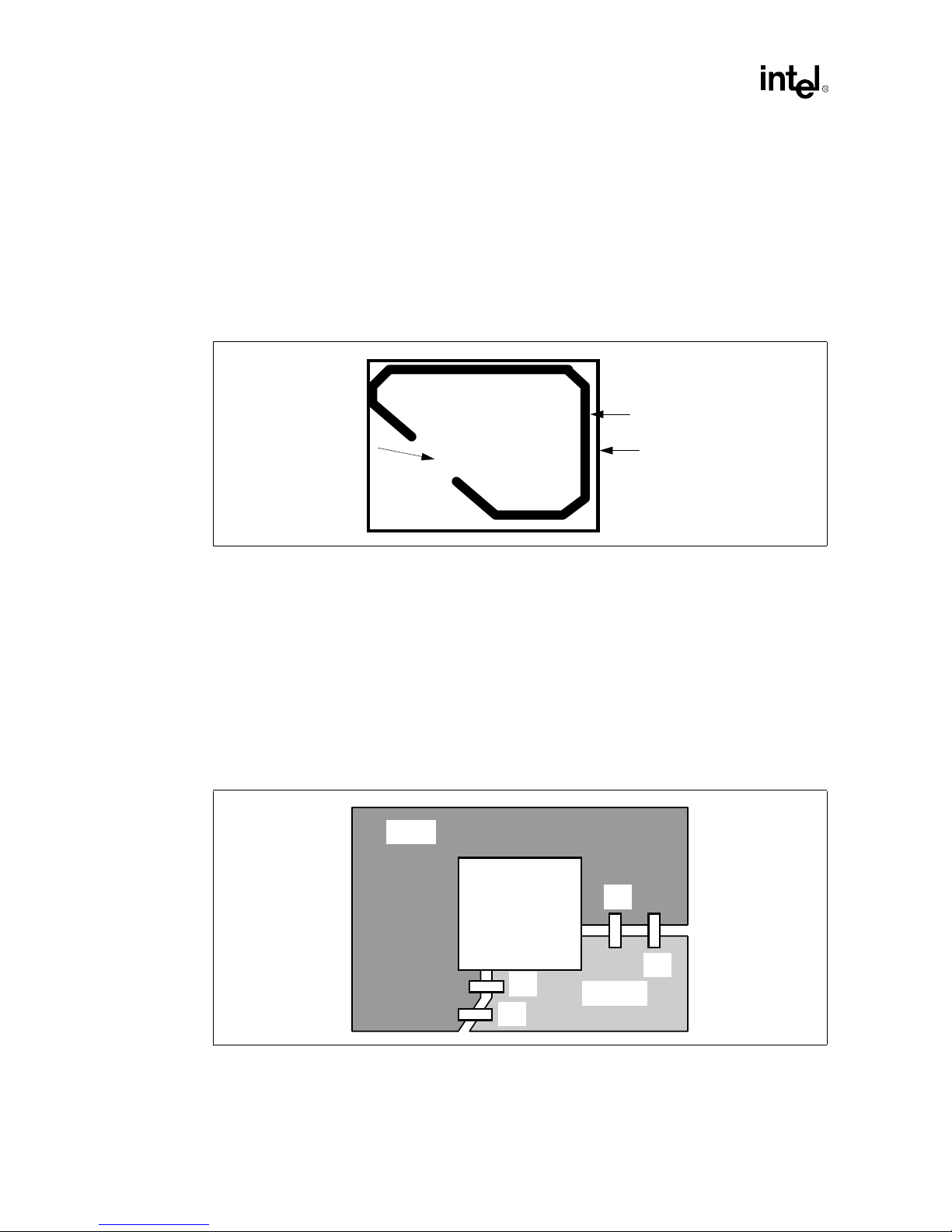
2.1.3.2 Fences
A “fence” is a line routed out of the plane such that a given area is isolated from the rest of the
plane except at a single point of contact, conceptually the “gate” in the fence. A fence will
minimize noise originating from digital signaling onto the analog signals. This provides higher
quality video for both the Bt829B and Bt869. An example of a fenced power plane is shown in
Figure 2-1. The heavy black line is the routed area. The width of the gate or opening can be up to
75% of the length of the IC in question. The widt h of the routed fence should conform to the
separation routing between power planes (i.e., 25 mils minimum).
Figure 2-1. Example of Power Plane Separation ("fencing")
“gate”
Plane
(e.g. VCC)
2.1.3.3 Stitching
Power plane “stitching” is required between the VCC3 and VDDQ3 planes. Stitching two isolated
planes together with capacitors allows a current return path for high frequency signals which pass
over split power planes. This helps to eliminate EMI. The six 0.1 µF capacitors coupling VCC3 to
VDDQ3 should be spaced evenly if possible. Note the VDDQ3 plane is only near the AGP
connector . An example of sti tchi ng is s hown in Figure 2-2. This figure illustrates the power planes
and, therefore, does not show signal traces between capacitors. The general rule for power plane
stitching is to have a capacitor placed between every four signals crossing the two planes. As an
example, there should be a capacitor, four signals, a capacitor, another four signals, and so forth
ending with a capacitor.
Figure 2-2. Example of Power Plane Stitching
VCC3
Fenced area
(e.g. AVCC)
Routed “fence”
Overlying Chip
2-4
cap
IC
cap
cap
VDDQ3
cap
Intel740™ Graphics Accelerator Design Guide
Page 19
2.2 Layout and Routing Guidelines
This chapter describes layout and routing recommendations to insure a robust design. These
guidelines should be followed as closely as possible. Any deviations from the guidelines listed here
should be simulated to insure adequate margin is still main tained in the design.
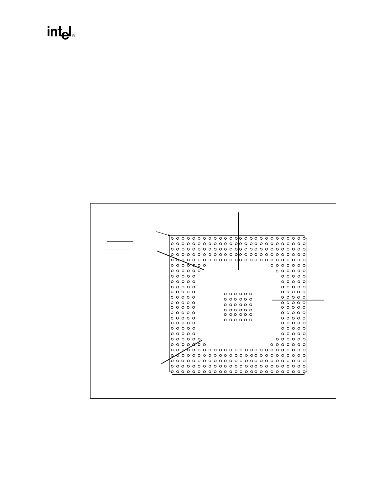
2.2.1 Placement
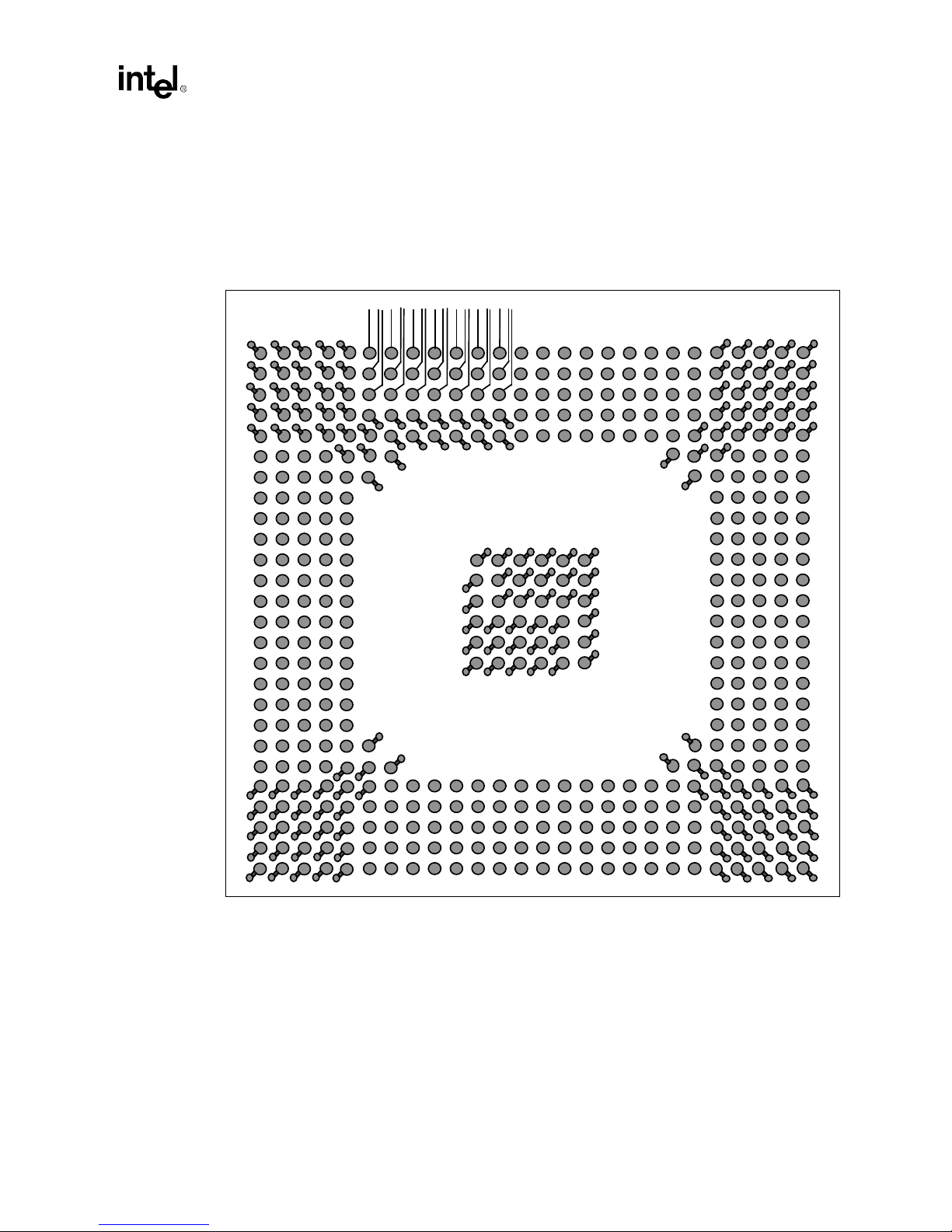
The ball connections on the Intel740™ graphics accelerator have b een assigned to simplify routing
and keep board fabrication costs down by enabling a 4-layer design. Figure 2-3 shows the four
signal quadrants of the Intel740 graphics accelerator. Component placement should be done with
this general flow in mind. This will simplify routin g and minimize the number of signals which
must cross. The individual signals within the respective groups have also been optimized to be
routed using only 2 PCB layers.
A complete list of signals and ball assignments can be found in the Intel740™ Graphics
Accelerator Datasheet.
Figure 2-3. Major Signal Sections
Addin Card Design
Intel740
Top View
Quadrant
Pin #1 Corner
A.G.P.
BIOS/Flicker
Quadrant
1 2 3 4 5 6 7 8 9 10 11 12 13 14 15 16 17 18 19 20 21 22 23
A
B
C
D
E
F
G
H
J
K
L
M
N
P
R
T
U
V
W
Y
AA
AB
AC
AD
AE
AF
Local Memory
VMI Port
Quadrant
Quadrant
Intel740™ Graphics Accelerator Design Guide
2-5
Page 20
Addin Card Design
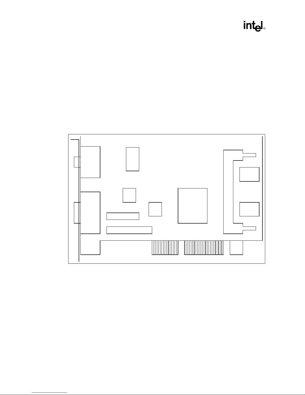
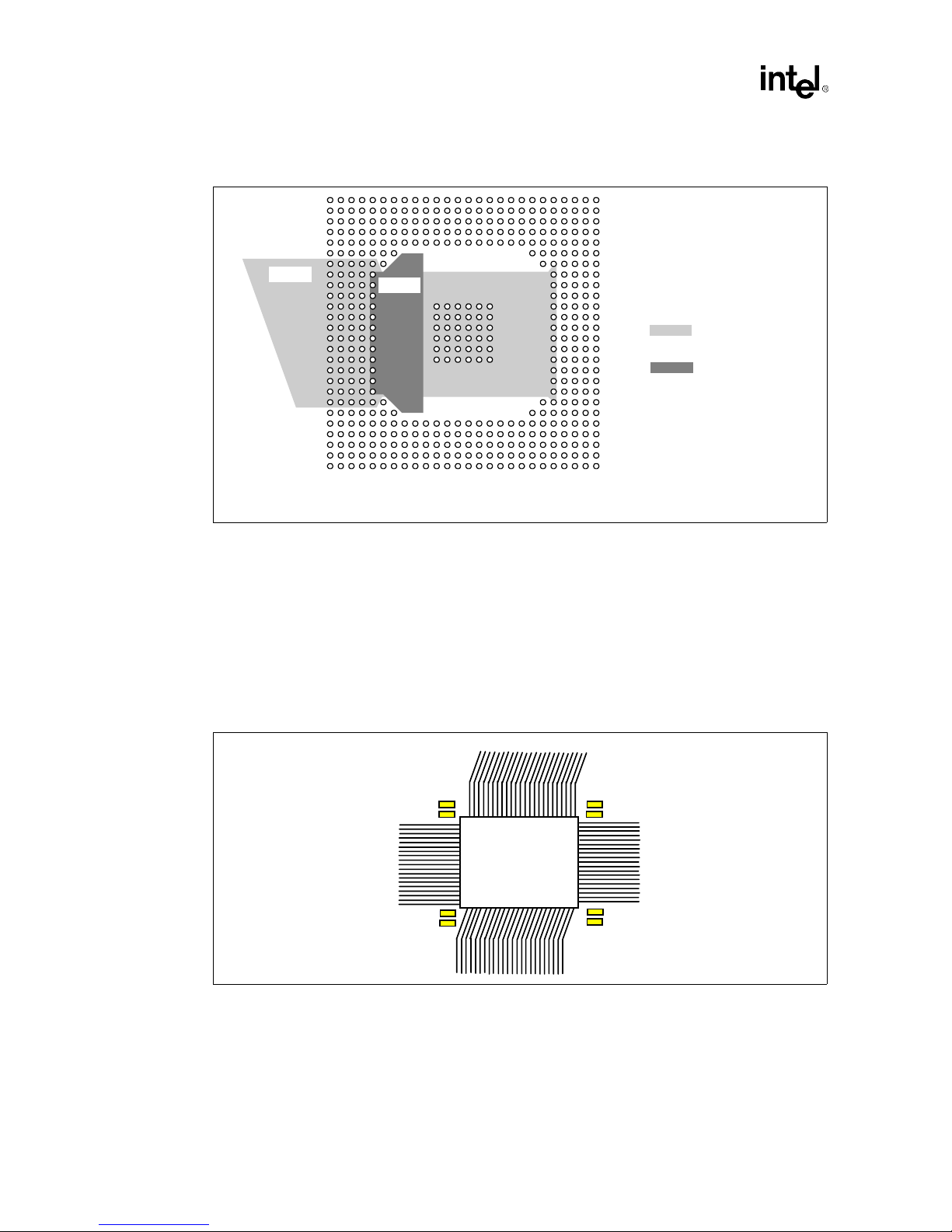
An example of the proposed component placement for an ATX form factor design is shown in
Figure 2-4. This is the placement used on the reference card. For NLX placement issues, refer to
Section 5.6, “NLX Considerations” on page 5-5.
ATX Form Factor:
•
The example placement (Figure 2-4) shows the Bt829B, Bt869, SO-DIMM Module, Intel740
graphics accelerator, VMI Port connections along with a 50 pin video connector.
•
The trace length limitation between critical connections will be addressed later in this
document.
•
Figure 2-4 is for reference only. The choice of size of memory, whether to have an SO-DIMM
connector, what video components to place on the board, and which video connectors to have
on the bracket will have to be evaluated by the board designer.
Figure 2-4. Example ATX Layout
VGA
Connector
Bt869
50 Pin
Connector
VMI Port
Connectors
2.2.2 Board Description
Bt829B
28F010
Flash
BIOS
Intel740™
Intel740
Chip
SO-DIMM
Connector
Memory
Memory
Even with the following recommendations, it is important to simulate your design.
A 4-layer stack-up arrangement is recommended. T he stack-up of the bo ard is shown in Figure 2-5.
The impedance of all the signal layers are to be between 50 and 80 ohms. Lower trace impedance
will slow signal edge rates, over & undershoot, and have less cross-talk than higher trace
impedance. Higher trace impedance will create faster edge rates and decrease signal flight times.
Prepreg is FR-4 material.
2-6
Intel740™ Graphics Accelerator Design Guide
Page 21
Figure 2-5. Four Layer Board Stack-up
Addin Card Design
Z = 65 ohms
Z = 65 ohms
Note: Top and bottom routing layers specify 1/2 oz. cu. However, by the time the board is plated, the
traces will end up with about 1 oz. cu. Please check with your fabrication vendor on the exact value
and insure that any signal simulation accounts for this.
Note: Thicker core helps reduce board warpage issues, while thinner prepreg reduces trace impedance.
Additional guidelines on board buildup, placement and layout include:
•
All layers should be cut back from the substrate outer edge by 0.050”. A 0.025”-wide strip
should be added to all signal and power layers around the outer edge and tied to the ground
plane.
•
All power and ground traces between vias and pads for all components should be at least as
wide as the component power or ground pad itself.
•
Through-hole vias, unless otherwise noted, are 10 mil drill, 25 mil diameter pad. Via capping
is required. All vias on the secondary side should be covered with solder mask. All vias on the
primary side are to be encroached with solder mask and anti-pad unless board dryness has
been guaranteed.
•
T o minimize solder wicking with the BGA, the component side solder mask should be applied
prior to tinning the copper. There should be no surface mount over bare copper (S.M.O.B.C.).
•
The solder mask must cover the trace between the via and pad.
•
The board impedance (Z) should be between 50 and 80 ohms (65 ohms ±20%).
•
FR-4 material should be used for the board fabrication.
•
The ground plane should not be split on the ground plane layer. If a signal must be routed for a
short distance on a power plane, then it should be routed on a VCC plane, not the ground
plane.
•
Keep vias for decoupling capacitors as close to the capacitor pads as possible.
•
Keep isolated power planes as close as possible to each other. This will minimize impedance
mismatch at the split.
•
All decoupling capacitors should be tied to the ground plane by a trace at least as wide as the
via ring to the plane.
6 mils
50 mils
6 mils
PREPREG
CORE
PREPREG
Primary Signal Layer (1/2 oz. cu.)
Ground Plane (1 oz. cu.)
Power Plane (1 oz. cu)
Secondary Signal Layer (1/2 oz. cu)
Total board width = 62 + .6 mils
Intel740™ Graphics Accelerator Design Guide
2-7
Page 22
Addin Card Design
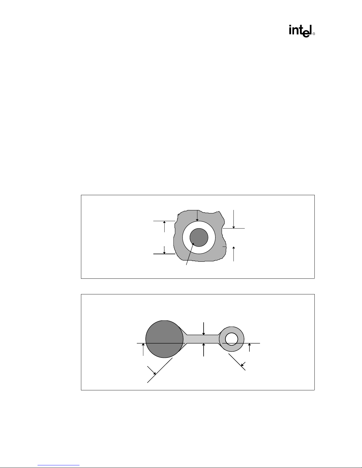
2.2.3 BGA Component
2.2.3.1 Layout Requirements
The following layout requirements should be followed when routing the 468 MBGA package.
•
All non-ground BGA lands should be Metal Defined (MD) lands with the following nominal
dimensions (see Figure 2-6).
— Metal pad: 20 (6/6 routing) / 24 mils (5/5 routing)
— Solder mask opening: 24 mil (20 mil pad) / 27 mils (24 mil pad)
•
Any trace connected to a MBGA land or PTH via in the MBGA land grid array should be
teardropped. The teardrop should leave the trace at a 45° angle and intersect the via
tangentially (see Figure 2-7).
•
The minimum distance between the gold finger edg e of the card and the center of the first row
of MBGA lands should be 525 mils, and 480 mils from the end of the start of the bevel.
•
All BGA ground vias should use 16 mil drill with no thermal reliefs.
Figure 2-6. Metal Defined land dimensions
Figure 2-7. BGA Trace
(.024”)
.027”
BGA Lan d
45°
Solder Mask Ope nin g
(.020”)
.024”
Metal Pad
Cover Trace with Solder M ask
PTH Via
45°
.010” min
Recommended to be as
wide as via
2-8
Intel740™ Graphics Accelerator Design Guide
Page 23
2.2.3.2 Ground Connections
Addin Card Design
All lands in the four corners and center are V
connect to an adjacent via which passes through to the solder side of the board, one via per ball,
with a trace as wide as the via. Heat will dissipate through these vias to the GND plane as well as to
the air on the solder side.
Figure 2-8. Dogbone Via Pattern
(GND). Thermal analysis requires that each Vss ball
ss
2.2.3.3 Power Connections
The VCC2 plane should be as wide as practical for high current-carrying capacity. Because of the
interspersing of VCC2 and VCC3 pins on the Intel740™ graphics accelerator, a polygon will be
needed on one of the signal layers to extend the VCC3 plane to the isolated VCC3 pins
(Figure 2-9). The VCC2 polygon is a separate plane on the VCC Layer; the darker VCC3 polygon
is a power flood on the solder side and connects to the VCC3 plane on the VCC Layer through vias.
Intel740™ Graphics Accelerator Design Guide
2-9
Page 24
Addin Card Design
p
p
p
p
p
Gr
Figure 2-9. Suggested VCC Planes for the Intel740™ Graphics Accelerator
VCC2
VCC3
2.2.3.4 Decoupling
Decoupling capacitors should ideally be placed as close as possible to the Intel740 graphics
accelerator. This means that the best decou
underneath the com
underneath the com
accelerator
the ca
ackage. At least a 0.1 µF and 0.01 µF are recommended for each corner. By placing
acitors in this location all of the traces can “break-out” from the BGA package on all four
sides.
Figure 2-10. Intel740™ Graphics Accelerator Decoupling
onent. If a single sided board is required and capacitors cannot be placed
onent then decoupling is recommended at the corners o f the I ntel740 graphics
VCC2 on VCC Layer
VCC3 on Secondary Side
Signal Layer
vcc_pl.vsd
ling will occur if the capacitors are placed directly
2-10
0.1uF
0.01uF
0.1uF
0.01uF
0.1uF
0.01uF
Intel740
Graphics
Accelerator
(468 BGA)
0.1uF
0.01uF
Intel740™ Graphics Accelerator Design Guide
Page 25
2.2.3.5 General Sign al Routing
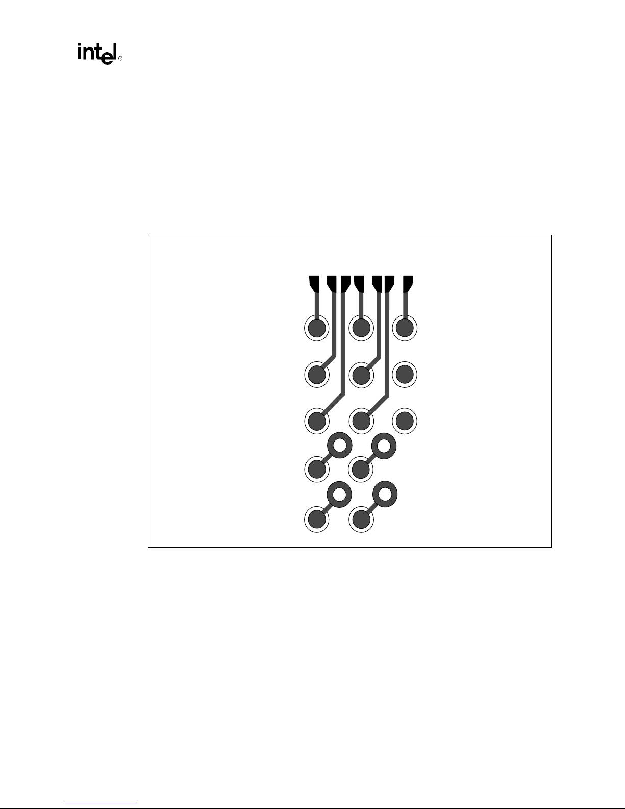
Figure 2-11 depicts general escape of traces from the five rows of BGA ball pads. The first three
ball rows can be routed on the primary layer. The last two must be routed through vias to the
secondary layer. Underneath the BGA, trace routing should be 5 on 5 or 6 on 6. Once the traces
have left the BGA, however, routing should expand to 5 o n 10 or 6 on 12. The ratio should be kept
as 1:2.
The signals AD _STB_A, AD_STB_B and SB_STB sh ould have a spacing of 1:4 to other signals.
Using this extra spacing between these specific signals will help to keep crosstalk to a minimum.
Addin Card Design
Figure 2-11.
Intel740™ Graphics Accelerator BGA Routing Exampl
COMPONENT SIDE ROUTING FOR 5 ROWS OF BALL PADS
R1
R2
R3
R4
e
2.2.4 Voltage Regulator
The physical tab (used as a built in heatsink) on the MOSFET package is the drain pin, and will
need a tab-shaped pad to solder to.
Note: The resistor/capacitor network between the COMP pin (pin 5) and the GND pin (pin 3) of the
LT1575 should be connected directly to the GND pin of the device rather than tied to the ground
plane.
2.2.5 Bt829 Video Decoder
Note: Rockwell* Semiconductor should be contacted for up to date layout recommendations.
Intel740™ Graphics Accelerator Design Guide
R5
2-11
Page 26
Addin Card Design
2.2.5.1 Ground Planes
The Bt829B and associated circuitry have two ground planes, GND and ANALOG_GND
(AGND). These are electrically the same plane but should be separated by a fence, as described in
Section 2.1.3.2, “Fences” on page 2-4. The schematic illustrates which pins attach to which plane
as does Table 2-3. The opening in the fence should be under the Bt829B and be up to 75% of the
IC’s width. The AGND plane is the isolated or subset plane, hence GND is the return path for
current. The AGND plane should be as small as possible.
Table 2-3. Bt829B GND and AGND Pins
GND 11, 21, 31, 33, 39, 77, 81, 90, 93, 95, 100
AGND 42, 47, 54, 56, 58, 61, 66, 71, 75
2.2.5.2 Power Planes
The Bt829 and associated circuitry have three power planes, VCC3, VCC and AVCC. The latter
two are digital and analog +5V, respectively. As above, these are electrically the same plane but
separated by a fence. This fence and the AVCC plane should parallel the AGND fence and plane
closely, with the opening in about the same location.
Bt829 Ground Pins
Table 2-4. Bt829B VCC and AVCC Pins
Bt829B 5V Pins
VCC 10, 38, 76, 88, 96
AVCC 40, 44, 48, 60, 65, 72
2.2.5.3 Passive Components and Signal Routing
All passive components should be placed as near to the Bt829B as possible. These parts include:
the 0.1µF and 0.01 µF bypass capacitors, the 10µF capacitors, the 75 ohm terminating resistors, an d
the crystal oscillator circuitry.
Note: There must be NO digital signals routed under or above the analog power and ground planes
(AVCC and AGND).
The filter circuits on the four video input signals (TUNER, SV_LUM, SV_CHR, CV_IN) need to
be located near the 50-pin connector. Note that other designs not using a 50 pin video connector
should have the filter circuits placed as close as possible to the input connectors. The analog traces
should not be routed such that they parallel other analog signals at a close spacing for a long length.
Wherever analog signals run in parallel, separated by less than 15 mils for longer than 250 mils,
run a ground line between them of approximately 12 mils width.
2.2.6 Bt869 Video Encoder
Note: Rockwell Semiconductor should be contacted for up to date layout recommendations.
2.2.6.1 Ground Planes
Only one ground plane is recommended for the Bt869. This ground plane should be formed as a
fence underneath the Bt869.
2-12
Intel740™ Graphics Accelerator Design Guide
Page 27
2.2.6.2 Power Planes
The Bt869 and associated circuitry have two power planes, VCC3 and 3VAA_BT869. The
3VAA_BT869 plane is a separate cutout, joined to VCC3 by a ferrite bead. The device should
reside entirely above the 3VAA_BT869 plane, as there are no VCC3 connections to the device. So
long as the 3VAA_BT869 plane underlies all the analog components, it should be as small as
possible.
Table 2-5. Bt869 Digital and Analog Power Pins
Bt869 3V Pins
3VAA_BT869 (Analog) 69, 71, 73, 80
3VAA_BT869 (Digital) 19, 20, 30, 40, 46, 47, 57, 60, 61
2.2.6.3 Passive Components and Signal Routing
All passive components should be placed as close to the Bt869 device as possible. These devices
consist of: the 0.1µF and 0.01µF bypass capacitors, the 10µF capacitors, the crystal oscillator
circuitry , and the 0.1 µF capacitors and 75 ohm resistors at the VREF, VBIAS and FSADJUST pins
as well as the protection diodes.
Addin Card Design
Note: There must be NO digital signals routed under or above the analog power and ground planes
(3VAA_BT869 and AGND).
The filter circuits on the three video output signals (TVOUT_Y, TVOUT_C, TVOUT_CVBS)
must be very near the 50-pin connector or other output connecto rs. Long leng ths of closely spaced
parallel analog signals should be avoided. Wherever analog signals run in parallel, separated by
less than 15 mils for longer than 250 mils, run a ground line between the video input traces of
approximately 12 mils width.
2.2.6.4 AGP Layout and Routing Guidelines
This section describes the group of signals that runs between the Intel740 graphics accelerator
AGP Interface and the AGP edge connector. For the definition of AGP functionality (protocols,
rules and signaling mechanisms, as well as th e platform level aspects of AGP functionality), refer
to the latest AGP Interface Specification. This document focuses onl y on specif ic Inte l740 grap hics
accelerator recommendations for the AGP interface. The gen eral len gth requir ements are shown in
Table 2-6.
Table 2-6. AGP Signal Lengths
Group Recommendation
All
CLK 2.6” ± 0.4”
Mismatch between strobe and data traces must be less than 0.5”. Thus the trace length for signals
within a group must be within ±0.5” of the corresponding strobe’s trace length, as indicated in
Table 2-7.
≤
3.0”
Table 2-7. Strobes and Corresponding Signal Groups
Group Strobe Recommendation
AD[31:16], C/BE[3:2]# AD_STB_B L
AD[15:0], C/BE[1:0]# AD_STB_A L
SBA[7:0] SB_STB L
Intel740™ Graphics Accelerator Design Guide
AD_STB_B
AD_STB_A
± 0.5”
SB_STB
± 0.5”
± 0.5”
2-13
Page 28
Addin Card Design
For example, AD29 and AD_STB_B must not be mismatched by more than 0.5”. No such
comparison, however, should be enforced between AD29 and AD30, or AD29 and C/BE2#, etc.
Note: AGP strobes must be separated by 2X no rmal signal spacing ( i.e., if no rmal spacing is 5/ 10 or 6/12,
the strobe signals must be separated from other traces by 20 or 24 mils, respectively).
2.2.6.5 Intel740™ Graphics Accelerator Memory Layout and Routing
Guidelines
The Intel740 graphics accelerator integrates a memory controller which supports a 64-bit memory
data interface. SGRAM can be used in addition to SDRAM if it is configured to perform as an
SDRAM. The Intel740 graphics accelerator generates the Row Address Strobe (SRAS[A:B]#),
Chip Selects (CS0[A:B]#, CS1[A:B]#), Column Address Strobe (SCAS[A:B]#), Byte Enables
(DQM[0:7]#), Write Enables (WE[A:B]#), and Memory Addresses (MA). The memory controller
interface is fully configurable through a set of control registers.
Eleven memory address signals (MAx[10:0]) allow the Intel740™ graphics accelerator to support
a variety of commercially available SO-DIMMs and components. Two SRAS# lines permit two
64-bit wide rows of SDRAM. All write operations must be one Quadword (QWord). The Intel740
graphics accelerator supports memory up to 100 MHz.
Rules for populating a Intel740 graphics accelerator Memory:
•
Memory can be populated using either an SO-DIMM or components.
•
SDRAM and SGRAM components and/or SO-DIMMs can be mixed.
•
The DRAM Timing register, which provides the DRAM speed grade control for the entire
memory array, must be programmed to use the timings of the slowest memories installed.
Possible DRAM and system options supported by the Intel740 graphics accelerator are shown in
Table 2-8.
Table 2-8. Supported Memory Options (Other Memory Options Are Not Supported)
SDRAM/
SGRAM
Technology
8 Mbit 256K 32 Asymmetric 10 8 2MB 4MB
16Mbit 512K 32 Asymmetric 11 8 4MB 8MB
16Mbit 1M 16 Asymmetric 12 8 8MB 8MB
SDRAM/
SGRAM
Density
SDRAM/
SGRAM
Width
Addressing Address Size
Row Column Min Max
There are several groups of signals within the memory bus with layout restrictions.
Table 2-9. Memory Layout Restrictions (See Figure 2-12 and Figure 2-13)
Signal Intel740™ to SO-DIMM SO-DIMM SGRAM Stub SGRAM Stub
Min Max Min Max Min Max
MA[11:0] n/a 4.0” 0.25” 0.9” 0.25" 0.6”
MD[63:0], DQM[7:0] n/a 3.0” 0.25” 0.9” 0.25" 0.4”
Local Memory
Size
2-14
Intel740™ Graphics Accelerator Design Guide
Page 29
Figure 2-12. Layout Dimensions (MA[11:0])
Intel740™
Intel740
Chip
4.0”
Addin Card Design
SGRAM
0.25” - 0.9”
0.25” - 0.6”
0.25” - 0.6”
SO-DIMM
SGRAM
Figure 2-13. Layout Dimensions (MD[63:0], DQM[7:0])
Intel740™
Intel740
Chip
3.0”
0.9”
0.4”
SGRAM
0.4”
SO-DIMM
SGRAM
Table 2-10. Memory Layout Restrictions (See Figure 2-14 and Figure 2-15)
Signal
WEA#, SRASA#, SCASA#,
CSA1#, CSB0#
WEB#, SRASB#, SCASB#,
CSA0#
Intel740™ to
SO-DIMM
Min Max Min Max Min Max
n/a 4.0” n/a n/a
n/a 4.0” 0.25” 0.9” 0.25” 0.6”
SO-DIMM to SGRAM
Stub
SGRAM Stub
Figure 2-14. Layout Dimensions (WEA#, SRASA#, SCASA#, CSA1#, CSB0#)
Intel740™ Graphics Accelerator Design Guide
Intel740™
Intel740
Chip
2.0” - 4.00”
SO-DIMM
2-15
Page 30
Addin Card Design
Figure 2-15. Layout Dimensions (WEB#, SRASB#, SCASB#, CSA0#)
SGRAM
2.0” - 4.0”
Intel740
Intel740
Chip
™
0.25” - 0.9”
SGRAM
0.25” - 0.6”
0.25” - 0.6”
Table 2-11. Memory Layout Restrictions (See Figure 2-16 and Figure 2-17)
Signal
TCLK0 0.6” 2.4” ±0.25” n/a n/a n/a
TCLK1 0.6” 2.4” ±0.25” 1.0” 0.4” 0.6”
Intel740™ to
Resistor
Resistor to
SO-DIMM
Figure 2-16. Memory Layout Dimensions (TCLK0)
0.6”
Intel740™
Intel740
Chip
0
Figure 2-17. Memory Layout Dimensions (TCLK1)
0.6”
Ω
SO-DIMM to
SGRAM Stub
2.4” +/- 0.25”
2.4” +/- 0.25”
SGRAM Stub
Min Max
SO-DIMM
Connector
Intel740™
Intel740
Chip
2-16
SO-DIMM
Connector
0
Ω
Intel740™ Graphics Accelerator Design Guide
Page 31

Addin Card Design
Signal Intel740™ to Resistor
OCLK to Resistor 2.75” ±0.25
RCLK0, RCLK1 3.0” ±0.25”
Note: It is important to match clock lengths. For example, if the length from OCLK to Resistor is 1.03,
then the length from Resistor to RCLK should be 3.03.
Figure 2-18. Memory Layout Dimensions (RCLK and OCLK to RCLK)
Intel740™
Intel740
2.75” +/- 0.25
Chip
OCLK
Ω
3.0” +/- 0.25”
33
RCLK0
3.0” +/- 0.25”
RCLK1
2.2.6.6 Intel740™ Graphics Accelerator Memory Configurations
In the following discussion the term row refers to a set of memory devices that are simultaneously
selected by an SRAS and the CS# signal.
Configuration #1: In this configuration, the minimum amount of memory (2MB) is supported.
Note that, the same copy of all control signals goes to each component.
Figure 2-19. 2/4 MB Local Memory Connection (64-bit data path)
33
Ω
Intel740™ Graphics Accelerator Design Guide
Intel740
MD[63:0]
CSx[A:B]# DQM[3:0] DQM[7:4] RCLKx OCLK
CS0A#
MD[31:0]
CS0A#
MD[63:32]
Intel740™ Chip
256K/512K X 32
256K/512K X 32
MA[11:0]
WEA#
SRASA#
SCASA#
TCLKA
WEA#
SRASA#
SCASA#
TCLKA
2-17
Page 32

Addin Card Design
Configuration #2: Two rows of memory are supported in this configuration. If 256Kx32
components are used 4MB of memory is obtainable, if 512Kx32 is used, then 8MB is supported.
Note that both rows of memory receive different copies of each control signal, for loading reasons.
Figure 2-20. 4/8 MB Local Memory Connection (64-bit data path)
Intel740™ Chip
Intel740
MD[63:0]
CSx[A:B]# DQM[3:0] DQM[7:4] RCLKx OCLK
MA[11:0]
MD[31:0]
MD[63:32]
MD[31:0]
MD[63:32]
CS0A#
CS0A#
CS1A#
CS1A#
256K/512K X 32
256K/512K X 32
256K/512K X 32
256K/512K X 32
WEA#
SRASA#
SCASA#
TCLKA
WEA#
SRASA#
SCASA#
TCLKA
WEB#
SRASB#
SCASB#
TCLKB
WEB#
SRASB#
SCASB#
TCLKB
2-18
Intel740™ Graphics Accelerator Design Guide
Page 33

Configuration #3: One row of memory is supported in this configuration using 1Mx16 SDRAMs.
Only the maximum allowable amount of memory (8MB) is supported in this configuration. Note
that each copied signal is sent to only two components.
Figure 2-21. 8 MB Local Memory Connection (64-bit data path)
Intel740™ Chip
MD[63:0]
Addin Card Design
Intel740
MA[11:0]
CSx[A:B]# RCLKx OCLK
CS0A#
MD[15:0]
CS0B#
MD[31:16]
CS0A#
MD[47:32]
CS0B#
MD[63:48]
DQM[1:0]
DQM[3:2]
DQM[5:4]
1M X 16
1M X 16
1M X 16
1M X 16
DQM[7:6]
WEA#
SRASA#
SCASA#
TCLKA
WEB#
SRASB#
SCASB#
TCLKB
WEA#
SRASA#
SCASA#
TCLKA
WEB#
SRASB#
SCASB#
TCLKB
Intel740™ Graphics Accelerator Design Guide
2-19
Page 34

Addin Card Design
2.2.6.7 TV Out Interface
The TV out bus is the group of s ignals that carry dig itized display da ta from the Intel740
graphics accelerator to the Bt869 flicker filter TV-out component. This interface is shared with
the BIOS interface. Table 2-12 gives the maximum trace lengths between components.
Table 2-12. TV Out/ROMA Trace Lengths (See Figure 2-22)
Signal
ROMA[17:0] 0.0” 3.5” 0.0” 1.5” 0.0” 4.0”
Intel740™ to BIOS
Stub
Min Max Min Max Min Max
Figure 2-22. Layout Dimensions, Digital TV Bus
Intel740™
Intel740
Chip
0.0” - 3.5”
BIOS ROM
2.2.6.8 Analog Signals
It is recommended that all analog signal traces be 75Ω ±5%. It is important that these traces not
violate the 5x10 mil spacing for the 65Ω traces. Analog traces include the DAC R, G, B traces, all
of the inputs to the Bt829B component and outputs from the Bt869 component.
2.2.7 UL and FCC Considerations
BIOS Stub BIOS to Bt869
0.0” - 4.0”
Bt869
0.0” - 1.5”
2-20
Certain precautions should be taken in the design of the of a graphics card to ensure passing safety
and EMI tests. These precautions are listed below.
•
When a signal can be hot plugged, clamping diodes should be used to limit voltage spikes.
•
When a voltage leaves the card, a fuse should be placed in the path to protect from a short
circuit.
•
Sockets, Fans and Brackets should be grounded.
•
Separate Power Planes of the same voltage should be stitched together.
Intel740™ Graphics Accelerator Design Guide
Page 35

2.3 Addin Card Schematics
This section describes the Intel740™ Graphics Accelerator Reference Design Schematics. Please
read this section carefully to observe all design recommendations and requirements.
The description of each schematic page is named by the logic block shown on that page.
Cover Sheet (Schematic Page 1)
The Cover Shee t shows the schem atic page titles, page numbers, dis claimers and power pins.
Block Diagram (Schematic Page 2)
This page shows a block diagram overview of the Intel740 AGP card design. Schematic page
numbers for each of the major schematic components are shown.
Intel740™ Graphics Accelerator (Schematic Pages 3,4)
This page shows all of the connections to the Intel740 graphics accelerator. Each Intel740 graphics
accelerator interface is hooked up in this reference design. Beginning in the upper left hand corner
of the page, the video capture port is shown. Internally, the input pins are pulled down. These pins
contain a strapping option for subsystem ID. In this case the reference design has an ID of 0100h.
Bits that should be a “1” may be pulled up using a 2K pull-up resistor. If the graphics design will
not have video, the only concern is pu lling the bus up to the correct value for the subsys tem ID.
The video control signals may be left unconnected. The BIOS interface multiplexes the BIOS,
vendor ID, and flicker filter TV encoder. The ROMA lines are internally pulled down and may be
pulled up using a 2K pull-up resistor. The video host port connects directly to the VMI header. The
section labeled AGP interface connects directly to the AGP connector. The memory interfaces
connect to an SO-DIMM connector and memory components. Each of the 9 GPIOs serve a
different function in the reference design. Table 2-13 lists the function assigned to the GPIOs.
Addin Card Design
Table 2-13. GPIO Functions
GPIO FUNCTION
GPIO0 I
GPIO1 I
GPIO2 DDC Data
GPIO3 DDC Clock
GPIO4 Fan Fail
GPIO5 Extra For DVD Control
GPIO6 VP[15:0] Bus Isolation Control
GPIO7 Extra For DVD Control
GPIO8 Power Down
Decoupling for the Intel740 graphics accelerator is shown along the bottom of the schematic page.
2
C Data
2
C Clock
Intel740™ Graphics Accelerator Design Guide
2-21
Page 36

Addin Card Design
Voltage Regulator (Schematic Page 5)
This page shows the circuitry to convert from 3.3 Volts to 2.7 Volts. The regulator used in the
reference design does not need any heat sink for the FET. As shown, the FET will be dissipating
slightly over 1 watt. If a different voltage regulator solution will be used, calculations will be
needed to determine the need for a heatsink. Resistors R50, R44, R42, and R43 are only for the
reference card design. These resistors allow different voltage combinations for core and internal
Intel740 graphics accelerator PLLs. The table at the top of the page describes the voltage
configurations. Core decoupling is shown at the bottom of the page and should be placed close to
the Intel740 graphics accelerator.
Bt829B (Sch ematic Page 6 )
The Bt829B component contains analog inputs which require special routing requirements detailed
in Section 2.2.5, “Bt829 Video Decoder” on page 2-11. If these analog inputs are not used, then
they should be tied to ground as is MUX3 in the reference design. The I2CCS pin is pulled low in
the reference design to select an I
connecting other I
Note: Care must be taken to ensure that no two devices use the same address.
The QCLK output of the Bt829B obviates the need for connection to the VRDY input on the
Intel740 graphics accelerator as this clock “ANDs” the ACTIVE and CLK outputs of the Bt829B
together. The reference design is designed to support NTSC, PAL and SECAM. If only NTSC is
desired, the circuitry including Y1 can be removed and XT1I should be tied high or low with
XT1O left floating. If only PAL mode of operation is desired, XT1I should be tied high or low with
XT1O floating and Y2 should be replaced with Y1. Decoupling for the component is shown at the
bottom of the page.
2
2
C devices like the Bt869.
C address of 88h and 89h. This selection becomes important if
Bt869 (Schematic Page 7)
The Bt869 power supply is generated from the VCC3 supply. Decoupling for this supply is shown
at the top of the page. The componen t contains a 24-bit data port. The In tel740 gr aphics acceler ator
connects only to 12 of these bits. The functionality of this interface is described in the Intel740
Graphics Accelerator Datasheet. The slave input is tied to ground to place this chip in m aster mode.
If the digital port were to be used as a VMI port, the component should be placed in slave mode.
This page contains the only jumper in the design. This jumper selects which mode (PAL or NTSC)
the Bt869 will operate in. The PC ’98 specification recommends this jumper for designs where a
TV may be the only output display. The ALTADDR pin is pulled high so that the device responds
to an address of 8Ah. This address keeps this device from conflicting with the Bt829B’s I
2
C
address. Note that ROMA17 is wired to the CLKI pin while ROMA14 is connected to the CLKO
pin. ROMA17 is also called CLKOUT and ROMA14 is called CLKIN. The Intel740’s graphics
accelerator CLKOUT pin corresponds to the Bt869’s CLKI pin while the CLKIN pin corresponds
to the CLKO pin on the Bt869. The DAC lines have special routing requirements detailed in
section. These DAC lines allow the component to output S-Video and composite video.
VMI Video Connectors (Schematic Page 8)
The VMI video connectors are used for the attachment of a DVD daughter card or video capture
card. The capture port is connected to the 26 pin header while the bi-directional host port is
connected to the 40 pin header. The reference design uses a 2A fuse for the 3.3 volt supply to the
40 pin header. The 2A fuse is allowed for the 5 volt supply and 1A is allowed for the 12 volt
supply . GPIO5 an d GPIO7 com e to the h eader for added DVD daughter card functionality control.
GPIO8 is used for power down operation on the card. The I
2
C connections on the 26 pin header are
3.3 volt signals. Mechanical dimensions for the placement of the connectors is shown in
Section 5.3, “VMI Header Placement” on page 5-2.
2-22
Intel740™ Graphics Accelerator Design Guide
Page 37

Addin Card Design
AGP Card Edge (Schematic Page 9)
This page details the connections of AGP. All power is derived from this connector. Using the rule
of 1A per pin, the 12 volt supply is capable of supplying 1A, the 5 Volt supply is capable of
supplying 2A and the 3.3 Volt supply is capable of supplying 8A.
VGA Connector
(Schematic Page 10)
The VGA connector provides the RGB output to a monitor. BIOS and hardware provide support
for plug-and-play capability.
2
DDC/I
This page details the 3.3 volt/5 volt signal conversion as well as the DDC/I
C (Schematic Page 11)
2
C connections. To
perform the voltage translation, quick switches are used. The quick switches at the top of the page
serve a second function of isolating the VMI port from the Intel740 graphics accelerator. GPIO6
can tri-state this bus to preclude the possibility of contention between something connected to the
VMI header and the Bt829B.
SO-DIMM Connector (Schematic Page 12)
The SO-DIMM connector shows a fairly straight forward connection to the Intel740 graphics
accelerator memory signals. Note that the primary CS0 connection is tied to the Intel740 graphics
accelerator CSA1# signal. The CSB0# signal is connected to CS1 on the connector. The reference
design has the first row of memory down on the graphics card. The second row of memory is
assumed to be placed in the SO-DIMM connector.
Note: It is important not to have the memory on the graphics card and memory on the SO-DIMM
connector connected to the same row.
SGRAMS (Schematic Page 13)
The SGRAMs shown on this page are labeled as 512Kx32. The schematic pinout is actually
capable of supporting either the 512Kx32 or 256Kx32 SGRAMs. This dual-support connection is
achieved through the following method. The 512Kx32 Jedec standard defines AP on pin 51 which
is address 9. BS is on pin 29 and is also labeled as address 10. Addres s 8 is on pin 30. The Int el740
contains the AP on its address 8 pin and BS on address 9 pin. Since the 256Kx32 has AP with
graphics accelerator address 8 and on pin 51 along with BS with address 9 on pin 29 and a no
connect on pin 30, either the 512K or the 256K SGRAMs are capable of being supported in the
same design (see Figure 2-23).
Note: It is important to disable the special features of SGRAM. This will make the SGRAM operate as an
SDRAM, thus making it compatible with the Intel740 graphics accelerator.
Intel740™ Graphics Accelerator Design Guide
2-23
Page 38

Addin Card Design
Figure 2-23. 512Kx32 and 256Kx32 Pinout Compatibility
Intel740™
Intel740
Chip
A8/AP
A9/BS
A10
A7
.
.
A0
Intel740™
Chip
Intel740
A8/AP
A9/BS
A10
A7
.
.
A0
Figure 2-24. 1M X 16 Pinout Compatibility
Pin 51
Pin 29
Pin 30
Pin 51
Pin 29
Pin 30
A9/AP
A10/BS
A8
A7
.
.
A0
A8/AP
A9/BS
NC
A7
.
.
A0
512Kx32
SGRAM
Jedec
Standard
256Kx32
SGRAM
Jedec
Standard
2-24
Intel740™
Chip
A11/BS
A10/AP
A9
A8
.
.
.
A1
A0
A11
A10
A9
A8
A1
A0
Intel740™ Graphics Accelerator Design Guide
.
.
.
1M X 16
SDRAM
Page 39

Addin Card Design
Video Connector (Schematic Page 14)
This page shows a specially designed solution to the problem of too many connectors and not
enough board space. This 50 pin connector allows external hookup for a tuner , S-V ideo in, S-V ideo
Out, composite video in, and composite video out. The input connections feed to the Bt829B
component while the out connections come from the Bt869. Individual designs may or may not
have all possible connectors and, therefore, may not need this type of solution.
BIOS/FAN (Schematic Page 15)
This page shows the connections to the flash BIOS and fan power. The BIOS used in this design is
a PLCC socket for early debug capabilities. To use less board space a TSOP package may be the
preferred component. Since the selected part is a 5 volt part, the data lines are isolated from the
Intel740 graphics accelerator by a level shifter.
Note: The Intel740 graphics accelerator does not require a fan for AGP compliant systems. These
design features have been added for ease of use if the customer determines a fan is required. Refer
to the Thermal Application Note and software to determine the correct thermal solution.
The fan powerdown control is done through the use of a FET. Normal operation of the fan is
allowed by the 4.7 KΩ pull-up resistor (R26). If powerdown is desired, the GPIO8 pin will turn the
FET off. Pin 3 of the fan header allows the fan to signal the I ntel740 graphics accelerator that it has
failed.
Intel740™ Graphics Accelerator Design Guide
2-25
Page 40

Addin Card Design
2-26
Intel740™ Graphics Accelerator Design Guide
Page 41

A
A
B
B
C
C
D
D
E
E
4 4
3 3
2 2
1 1
INTEL740(TM) GRAPHICS ACCELERATOR FULL FEATURED REFERENCE CARD
TITLE
P.1
P.2
P.3
P.4
P.5
P.6
P.7
P.8
P.9
P.10
P.11
P.12
P.13
P.14
P.15
P.16
P.17
PAGE
COVER SHEET
BLOCK DIAGRAM
INTEL740(TM) GRAPHICS ACCELERATOR (A)
INTEL740(TM) GRAPHICS ACCELERATOR (B)
VOLTAGE REGULATOR
BT829B VIDEO DECODER
BT869 VIDEO ENCODER
VMI VIDEO CONNECTOR
AGP CONNECTOR
VGA CONNECTOR
VMI/DDC/I2C/FANFAIL LEVEL SHIFTER
SO-DIMM
SGRAM
VIDEO CONNECTORS
BIOS/FAN CONNECTOR
REVISION HISTORY
+12V = 12V ANALOG UNLESS OTHERWISE SPECIFIED
VCC = 5V DIGITAL UNLESS OTHERWISE SPECIFIED
VCC3 = 3.3V DIGITAL UNLESS OTHERWISE SPECIFIED
VDDQ = 3.3V AGP POWER SUPPLY
VCC_CORE = VOLTAGE SUPPLIED TO THE INTEL740 CHIP CORE
GND = DIGITAL GND
VCC
VCC3
VDD
THIS SPECIFICATION IS PROVEDED AS IS WITH NO WARRANTIES
WHATSOVER, INCLUDING ANY WARRANTY OF MERCHANTABILITY, FITNESS
FOR ANY PARTICULAR PURPOSE, OR ANY WARRANTY OTHERWISE ARISING
OUT OF PROPOSAL, SPECIFICATION OR SAMPLE.
NO LICENSE, EXPRESS OR IMPLIED, BY ESTOPPEL OR OTHERWISE, TO
ANY INTELLECTUAL PRPERTY RIGHTS IS GRANED HEREIN.
INTEL DISCLAIMS ALL LIABILITY, INCLUDING LIABILITY FOR
INFRINGEMENT OF ANY PROPRIETARY RIGHTS, RELATING TO USE OF
INFORMATION IN THIS SPECIFICATION. INTEL DOES NOT WARRANT
OR REPRESENT THAT SUCH USE WILL NOT INFRINGE SUCH RIGHTS.
I2C IS A TWO-WIRE COMMUNICATIONS BUS/PROTOCOL DEVELOPED BY
PHILIPS. SMBUS IS A SUBSET OF THE I2C BUS/PROTOCOL AND WAS
DEVELOPED BY INTEL. IMPLEMENTATIONS OF THE I2C BUS/PROTOCAL
OR THE SMBUS BUS/PROTOCOL MAY REQUIRE LICENSES FROM VARIOUS
ENTITIES, INCLUDING PHILIPS ELECTRONICS N.V. AND NORTH
AMERICAN PHILIPS CORPORATION.
*THIRD-PARTY BRANDS AND NAMES ARE THE PROPERTY OF THEIR
RESPECTIVE OWNERS.
COPYRIGHT * INTEL CORPORATION 1997
+12V
Intel740(TM) Graphics Accelerator Reference Card
2.1
Cover Sheet
C
1 16Thursday, April 09, 1998
Title
Size Document Number Rev
Date: Sheet of
Page 42

A
A
B
B
C
C
D
D
E
E
4 4
3 3
2 2
1 1
VIDEO CONNECTORS
p. 14
VIDEO
DECODER
p. 6
VMI CONNECTOR
p. 8
VOLTAGE REGULATOR
p. 5
SO-DIMM
p. 12
A.G.P. CONNECTOR
p. 9
VGA/DDC
CONNECTOR
p. 10
TV TUNER
CONNECTOR
p. 14
VIDEO
ENCODER
INTEL740(TM)
Graphics Accelerator
p. 3, 4
p. 7
p. 13
GRAPHICS
MEMORY
FLASH
p. 15
BIOS
CNTL
ADDR
DATA
ADDR/DATAA
ADDR/DATA
CNTL
AGP SIDEBAND
Intel740(TM) Graphics Accelerator Reference Card
2.1
Block Diagram
B
2 16Thursday, April 09, 1998
Title
Size Document Number Rev
Date: Sheet of
Page 43

A
A
B
B
C
C
D
D
E
E
4 4
3 3
2 2
1 1
INTEL740 (A)
VENDOR ID IS 0X8086
NOTE:
----THIS I.D. NEEDS TO
REFLECT BOARD VENDOR
SUBSYSTEM ID IS 0X100
1%
1%
1%
USE TANTALUM CAPACITORS FOR 10 AND 22UF
Intel740(TM) Graphics Accelerator Reference Card
2.1
Intel740(TM) Graphics Accelerator(A)
C
3 16Thursday, April 09, 1998
Title
Size Document Number Rev
Date: Sheet of
TP_03J26
SBA7
SBA1
ROMA7
ROMA2
TP_03L24
AD21
3VVP14
AD30
AD22
AD12
ROMA13
ROMA5
3VVP2
ROMA0
SBA4
AD2
ROMA11
3VROMD4
3VROMD2
3VROMD0
AD26
AD17
AD6
ROMA14
ROMA9
3VVP3
AD31
AD5
AD3
3VVP7
3VVP4
3VVP0
3VROMD1
ST1
SBA6
AD23
AD4
IREFSET#
SBA0
AD28
AD13
3VVP11
ROMA15
AD1
ROMA8
ROMA1
ST0
AD27
AD25
AD19
ROMA10
ROMA6
VMIHA3
AD20
AD8
ROMA16
SBA5
SBA3
3VVP12
ROMA4
ROMA3
VMIHA0
AD9
AD7
3VVP9
3VVP5
VMIHA4
VMIHA2
TP_03L23
3VVP15
AD10
AD15
3VVP8
AD14
ST2
AGPREF
3VROMD5
AD29
ROMA17
3VROMD3
AD24
AD18
3VVP10
ROMA12
VMIHA1
SBA2
AD11
3VVP13
AD16
3VVP6
AD0
3VROMD7
3VROMD6
3VVP1
VCC3
VCC3
VDDQ
VCC_CORE VCC3 VDDQ VCC3
VCC3
VDDQ
VDDQ
VCC3
VCC3
R22
2K
R472KR522KR512KR55
2K
C127
.01UF
R60
182
R59
267
R24
562
AGP INTERFACE
VIDEO CAPTURE
BIOS INTERFACE
U9A
INTEL740
VCC
E07
VP15
B21
VCC
F25
VCC
E09
VSS
AE23
VRDY#
J24
VCCA
G23
VCC
E11
VSS
AE24
VCCP
G25
VCC
E13
HREF#
K22
VCC
E14
VSS
AE25
VCC
E16
VCCA
G26
VCC
E18
VREF#
L23
VCC
E20
VSS
AE26
VCC
H22
VCLK
L24
VCC
AB07
VSS
AF01
VCC
AB09
VSS
AF02
VCC
AB11
VSS
AF03
VCC
AB13
VSS
F06
VCC
AB14
VSS
F07
VCC
AB18
VSS
F20
VCC
AB16
VCC
AB20
VSS
F21
VSS
F22
VSSA
F23
VSS
G06
VSS
G21
VSSA
H24
VSS
AF04
VSS
AF05
VSS
AF22
VSS
A01
VCCP
D06
VSS
A02
VCCP
AC06
VSS
A03
VCCP
E08
VDDQ
GO5
VSS
B05
VSS
B22
VSS
B23
VSS
B24
VSS
B25
VSS
B26
VSS
C01
VSS
C02
VSS
C03
VSS
C04
VSS
C05
VSS
C22
VSS
C23
VSS
C24
VSS
C25
VSS
C26
VSS
D01
VSS
D02
VSS
D03
VSS
D04
VSS
D05
VSS
D22
VSS
D23
VSS
D24
VSS
D25
VSS
D26
VSS
E01
VSS
E02
VSS
E03
VSS
E04
VSS
E05
VSS
E06
VSS
E21
VSS
E22
VSS
E23
VSS
E24
VSS
E25
VSS
E26
VSSA
F03
VSS
F05
VCCP
E10
VCCP
AB08
VCCP
E12
VCCP
D13
VCCP
AB10
VCCP
D14
VDDQ
J05
VCCP
E15
VCCP
AB12
VCCP
E17
VCCP
E19
VCCP
AC13
VDDQ
L05
VCCP
AC14
VCCP
AB15
VDDQ
N05
VCCP
AB17
NC
H26
VCCP
AB19
VDDQ
P05
VCCP
AC21
VCCP
Y22
VDDQ
T05
VCCP
V22
VCCP
T22
VDDQ
V05
VCCP
P22
VCCP
N22
VDDQ
Y05
VCCP
L22
VCCP
J22
VCCP
G22
NC
H25
VSS
A04
VSS
A05
VSS
A22
VSS
A23
VSS
A24
VSS
A26
VSS
B01
VSS
B02
VSS
B04
VSS
A25
VSS
B03
ST0
G01
VMIHA0
A16
ST1
H04
ROMD0
B07
ST2
H03
VMIHA1
D15
ROMA0
A07
VMIHA2
C15
ROMD1
A06
VMIHA3
B15
VP0
C17
VMIHA4
A15
ROMD2
B06
ROMA1
B08
ROMD3
C06
C/BE0#
V04
ROMD4
D07
ROMA2
A08
ROMD5
C07
VP1
A18
ROMD6
D08
ROMA3
B09
ROMD7
C08
AD0
Y04
ROMOE#
C09
ROMA4
A09
ROMWE#
C13
VP2
D17
ROMA5
B10
C/BE1#
U01
ROMA6
A10
VP3
B18
ROMA7
B11
AD14
U02
ROMA8
D11
VP4
C18
ROMA9
C10
C/BE2#
R01
ROMA10
D09
VP5
A19
ROMA11
D10
AD1
Y02
ROMA12
A11
VP6
D18
ROMA13
C11
C/BE3#
M03
ROMA14
D12
VP7
B19
ROMA15
B12
AD2
Y03
ROMA16
A12
VP8
C19
ROMA17
C12
AD15
T04
VP9
A20
AD3
Y01
VP10
D19
AD4
W05
VP11
B20
AD16
P03
VP12
C20
AD5
W03
VP13
A21
AD6
W04
VP14
D20
AD17
P02
AD7
W02
AD8
V02
AD18
P04
AD9
V03
AD10
V01
AD19
P01
AD11
U05
AD12
U03
AD20
N03
AD13
U04
AD21
N01
AD22
N04
AD23
N02
AD24
M04
AD25
M02
AD26
M05
AD27
L01
AD28
L03
AD29
L02
AD30
L04
AD31
K01
CLK
F02
SBA0
H01
SBA1
J04
SBA2
J02
SBA3
J03
SBA4
K03
SBA5
K05
SBA6
K02
SBA7
K04
RESET#
G03
INT
G04
STOP#
R05
PAR
T03
TRDY#
R04
IRDY#
T01
FRAME#
R03
DEVSEL
T02
REQ#
G02
GNT
H05
IREFSET#
D21
VSS
L25
VSSA
AA02
VMIINT#
B17
VMIRDY
A17
VMIRD#
D16
VMIWR#
C16
VMICS#
B16
DBF#
H02
SBSTB
J01
ADSTB_0
W01
ADSTB_1
M01
AGPREF
R02
LEFT
J23
VSS
L11
VSS
L12
C117
.1UF
C123
.1UF
C98
.01UF
C133
.01UF
C121
10UF
C132
.1UF
C44
.01UF
C112
.1UF
C131
.1UF
C130
.1UF
C110
.1UF
C17
22UF
C70
.01UF
C113
.1UF
C126
.1UF
C39
10UF
C111
.1UF
C128
.1UF
C116
.01UF
C114
.01UF
C124
.1UF
C125
.1UF
C54
.1UF
C76
.01UF
C109
.01UF
C115
.01UF
C74
.1UF
3VVP[15:0]6,11
3VROMD[7:0]15
ROMA[17:0]7,15
VMIHA[4:0]8
AD[31:0] 9
ST[2:0] 9
SBA[7:0] 9
3VVMIRDY11
3VVREF6,11
3VVMIINT#11
FRAME# 9
3VVCLK6,11
PAR 9
3VVRDY11
VMIWR#8
ROMWE#15
GNT# 9
AD_STB_A 9
VMIRD#8
AD_STB_B 9
VMICS#8
DEVSEL# 9
STOP# 9
CLK 9
CBE3# 9
CBE1# 9
ROMOE#15
CBE0# 9
IRDY# 9
INTA# 9
RESET# 6,7,8,9
TRDY# 9
CBE2# 9
3VHREF6,11
SB_STB 9
DBF# 9
REQ# 9
Page 44

A
A
B
B
C
C
D
D
E
E
4 4
3 3
2 2
1 1
OSC
U9
Intel740(TM) Graphics Accelerator Reference Card
2.1
Intel740(TM) Graphics Accelerator(B)
B
4 16Thursday, April 09, 1998
Title
Size Document Number Rev
Date: Sheet of
TP_03AE08
MD54
MD57
MD21
MD40
MD31
MD41
MD43
MD46
MD48
MD52
MA1
MD20
MD1
MD25
MD28
MD29
MD6
TP_03AA24
MD33
RCLK0
MD55
MD60
MA7
MA10
RT0
RCLK1
MD16
MD19
TDLY
MD51
MA2
DQM5
MD59
MA4
MD23
MD2
MD5
MD7
MD4
DQM1
DQM2
DQM7
MD3
MD27
MD14
MD17
TP_03AE14
MA0
DQM3
GFX_OSC
MD42
MD35
MD49
MD63
MA8
MD22
MD18
MD32
MD34
MD45
MD62
MA9
MD0
MD15
TP_03N25
MA6
MA11
MD11
MD13
DQM0
MD50
MD61
MD10
TP_03V24
MA3
MA5
TP_03Y26
MD36
MD37
MD58
MD30
MD26
MD9
MD12
MD44
MD39
MD47
MD38
MD53
MD56
DQM6
MD24
RT1
DQM4
MD8
VCC3
VCC3
VCC_PLL
VCC3
R37
33
R7
20K
R49
4.7K
R61
4.7K
R5
20K
Y3
66.6667MHZ
OUT3OE
1
VCC34GND
2
R46
33
R45
33
R38
33
DRAM INTERFACE
MEMORY DATA BUS
DISPLAY INT
INTEL740
VSS
AF23
OCLK
AD21
VSS
AF24
TCLKA
AF21
VSS
AF25
VSS
L13
VSS
AF26
TCLKB
AE21
VSS
L14
VSS
L15
VSS
L16
VSS
M11
VSS
M12
VSS
M13
VSS
M14
VSS
M15
VSS
M16
VSS
N11
VSS
N12
VSS
N13
VSS
N14
VSS
N15
VSS
N16
VSS
P11
VSS
P12
VSS
P13
VSS
P14
VSS
P15
VSS
P16
VSS
R11
VSS
R12
VSS
R13
VSS
R14
VSS
R15
VSS
R16
VSS
T11
VSS
T12
VSS
T13
VSS
T14
VSS
T15
VSS
T16
VSS
Y06
VSS
Y21
VSSA
AA03
VSS
AA05
VSS
AA06
VSS
AA07
VSS
AA20
VSS
AA21
VSS
AA22
VSS
AB01
VSS
AB02
VSS
AB03
VSS
AB04
VSS
AB05
VSS
AB06
VSS
AB21
VSS
AB22
VSS
AB23
VSS
AB24
VSS
AB25
VSS
AB26
VSS
AC01
VSS
AC02
VSS
AC03
VSS
AC04
VSS
AC05
VSS
AC22
VSS
AC23
VSS
AC24
VSS
AC25
VSS
AC26
VSS
AD01
VSS
AD02
VSS
AD03
VSS
AD04
VSS
AD05
VSS
AD22
VSS
AD23
VSS
AD24
VSS
AD25
VSS
AD26
VSS
AE01
VSS
AE02
VSS
AE03
VSS
AE04
VSS
AE05
VSS
AE22
MD40
U22
MD31
AE15
GPIO0
K23
RSVD
AA24
MD32
W22
MD41
V25
GPIO1
K24
MD33
Y25
MD42
U23
GPIO4
C14
MD34
W23
MD43
V26
RSVD
AE08
GPIO5
B14
MD35
Y26
MD44
U24
DQM0
AD10
MD36
W24
GPIO6
A14
MD45
U25
RSVD
AE14
MD46
T23
MD39
W26
GPIO7
B13
RCLK0
AC11
MD47
U26
GPIO8
A13
RSVD
V24
MD48
R24
MA0
AD17
MD49
R25
RSVD
N25
MD50
P23
RCLK1
T24
DQM1
AF10
MD51
R26
MD37
W25
MD52
P24
MD38
V23
DQM2
AD11
MD53
P25
MA1
AF16
MD54
N24
DQM3
AE11
MD55
P26
MD56
N23
DQM4
R22
MD57
N26
MA2
AC17
MD58
M24
DQM5
T25
MD59
M26
MD60
M23
DQM6
R23
MD61
M25
MA3
AE16
MD62
M22
DQM7
T26
MD63
L26
MA4
AD18
MA5
AF17
MD20
AD13
MA6
AC18
MA7
AE17
MA8
AD19
MA9
AF18
MA10
AC19
MA11
AE18
MD0
AD06
MD30
AC16
MD21
AF12
MD22
AD14
MD1
AE06
MD23
AE13
MD24
AD15
MD2
AC07
MD25
AF13
MD26
AC15
MD3
AF06
MD27
AF14
MD28
AD16
MD4
AD07
MD29
AF15
MD5
AF07
MD6
AC08
MD7
AE07
MD8
AD08
MD9
AF08
MD10
AC09
MD11
AE09
MD12
AD09
MD13
AF09
MD14
AC10
MD15
AE10
MD16
AC12
MD17
AF11
MD18
AD12
MD19
AE12
CKE
AA23
XTAL1
H23
WEA#
AE19
WEB#
AF19
SRASA#
AF20
SRASB#
AE20
SCASA#
AD20
SCASB#
AC20
CSA0#
AA25
CSA1#
AA26
CSB0#
Y23
CSB1#
Y24
RED
F24
GREEN
F26
BLUE
G24
VSYNC
J25
HSYNC
J26
DDCCLK
K26
DDCDATA
K25
IWASTE
C21
VCCDP
F01
VCCAP
F04
VCCDP
AA01
VCCAP
AA04
MD[63:0]12,13
DQM[7:0] 12,13
TCLK0 12
TCLK1 13
GPIO5 8
GPIO6 11
GPIO7 8
GPIO8 6,7,8,15
MA[11:0] 12,13
3VSCL 6,7,8,11,12
RED 10
GPIO4 15
HSYNC 10
CKE12,13
SCASB# 13
GREEN 10
CSA1# 12
BLUE 10
SCASA# 12
VSYNC 10
CSB0# 12
WEA# 12
3VDDCDA 11
WEB# 13
SRASA# 12
SRASB# 13
3VSDA 6,7,8,11,12
CSA0# 13
3VDDCCL 11
Page 45

A
A
B
B
C
C
D
D
E
E
4 4
3 3
2 2
1 1
RECOMMENDED HEXFET:
-------------------------MOTOROLA PART# MTD3055VLT4
SAMSUNG CORNING CO. LTD
PART# SSR3055-TM
NOTE:
---THE NET CONNECTING C60 TO C61
SHOULD BE CONNECTED DIRECTLY
TO PIN 3 OF THE LT1575 DUE TO
THE GROUND BOUNCE SENSIVITITY OF
THE LT1575 COMPENSATION PIN
TO VARY THE OUTPUT VOLTAGE, REPLACE
R40 WITH THE FOLLOWING VALUES TO
ACHIEVE THE VARIOUS OUTPUT
VOLTAGES:
R40 VOUT
----------------------------- 150 2.7V
160 2.8V
170 2.9V
180 3.0V
POWER CONFIGURATION*
R50 R44 R42 R43 CORE PLL____________________________________________________
STUFF EMPTY STUFF EMPTY 3.3V 2.7V
EMPTY STUFF STUFF EMPTY 2.7V 2.7V
STUFF EMPTY EMPTY STUFF 3.3V 3.3V
EMPTY STUFF EMPTY STUFF 2.7V 3.3V *DEFAULT
* THE DEFAULT POWER CONFIGURATION
IS NOT REPRESENTED HERE
Intel740(TM) Graphics Accelerator Reference Card
2.1
Voltage Regulator
A
5 16Thursday, April 09, 1998
Title
Size Document Number Rev
Date: Sheet of
L_GATE
COMP1
FB1575
R_GATE
M_COMP1
VCC_REGULATED
VCC3
+12V
VCC_CORE
VCC_PLL
VCC_CORE
U7
LT1575
SHDN
1
VIN
2
GND
3
FB4COMP
5
GATE
6
INEG
7
IPOS
8
C53
1UF
C40
100UF
R36
4.7
C52
1UF
R41
120
R35
7.5K
C61
1000PF
C60
10PF
R40
150
Q2
HEXFET
DRN
2
GATE
1
SRC
3
R50
0
R44
0
R42
0
R43
0
C86
22UF
C75
10UF
C64
.1UF
C80
.1UF
C81
.01UF
C65
.01UF
C63
.1UF
C62
.1UF
C87
.01UF
C89
.01UF
C88
.1UF
C82
.01UF
Page 46

A
A
B
B
C
C
D
D
E
E
4 4
3 3
2 2
1 1
DECOUPLING FOR ANALOG FENCE
TIE PINS TO
ANALOG FENCE
NOTE: ANALOG PLANE NEEDS TO BE FENCED FROM THE DIGITAL PLANE
Intel740(TM) Graphics Accelerator Reference Card
2.1
Bt829B Video Decoder
B
6 16Thursday, April 09, 1998
Title
Size Document Number Rev
Date: Sheet of
3VVP1
3VVP2
3VVP3
3VVP4
3VVP5
3VVP6
3VVP7
3VVP8
3VVP9
3VVP10
3VVP11
3VVP12
3VVP13
3VVP14
3VVP15
MUXOUT_YIN
TP_0582
TP_0578
TP_0589
MUX0
MUX1
MUX2
TP_0599
TP_0597
TP_0584
TP_0586
CCVALID
XT1I
XT1O
XT0I
XT0O
CIN
AGCCAP
REFOUT
CLEVEL
TP_0532
3VVP0
XT1CAP XT0CAP
TP_0559
VCC
VCC3
VCC3
VCC3
VCC
VCC3
VCC
VCCVCC3
C1
1UF
C27
1UF
C6
.1UF
R26
10K
R11
1M
R18
1M
Y1
35.46895MHZ
Y2
28.63636MHZ
C21
22PF
C33
22pF
C23
68PF
L3
2.7UH
C22
22pF
C35
100PF
C34
22pF
C38
1UF
C5
.1UF
C2
.1UF
R1075R17
75
R19
75
R9
75
C12
10UF
C48
.01UFC7.1UF
C51
.01UF
C16
10UF
C43
.1UF
C45
.01UF
C100
.1UF
C101
.01UF
C13
10UF
C14
10UF
C32
.01UF
C29
.1UFC4.01UFC3.1UF
C28
1UF
C49
.1UF
L6
2.7UH
BT829B
U4
GND
75
GND
71
GND
66
GND
61
GND
58
GND
56
GND
54
GND
47
GND
42
NC
68
NC
101
NC
51
NC
46
NC
63
NC
70
NC
69
GND11GND21GND31GND33GND39GND77GND81GND90GND93GND95GND
100
TRST*
35
TDO
32
TDI
37
TMS
36
TCK
34
AVCC
40
AVCC
48
AVCC
44
VD0
29
AVCC
60
AVCC
65
VD1
28
AVCC
72
VD2
27
VD3
26
VD4
25
VD5
24
VD6
23
VD7
22
VD8
9
VD9
8
VD10
7
VD11
6
VD12
5
VD13
4
VD14
3
VD15
2
FIELD
78
REFOUT
43
CBFLAG
89
MUX0
55
HRESET*
82
MUX1
57
VRESET*
79
MUX2
45
ACTIVE
83
MUX3
50
MUXOUT
53
AGCCAP
41
YIN
52
CIN
67
SYNCDET
59
YREF+
49
YREF-
62
CREF+
64
CREF-
73
CLEVEL
74
QCLK
94
DVALID
84
CCVALID
87
VACTIVE*
86
OEPOLE
85
XT0I
12
XT0O
13
XT1I
16
XT1O
17
CLKX1
97
CLKX2
99
NUMXTAL
80
PWRDN
91
OE*
98
RST*
15
I2CCS
14
SDA
18
SCL
19
VCC10VCC38VCC76VCC88VCC
96
VCC31VCC320VCC330VCC3
92
3VVP[15:0] 3,11
3VVREF 3,11
3VHREF 3,11
SV_LUM14
CV_IN14
TUNER14
3VSCL4,7,8,11,12
RESET#3,7,8,9
3VSDA4,7,8,11,12
SV_CHR14
GPIO84,7,8,15
3VVCLK 3,11
Page 47

A
A
B
B
C
C
D
D
E
E
4 4
3 3
2 2
1 1
NOTE:
ANALOG PLANE NEEDS TO BE FENCED FROM THE DIGITAL PLANE
PRIMARY SIGNALS SHOULD NOT CROSS CUTOUT
PINS 1-2 = NTSC
PINS 2-3 = PAL
NOTE: MAKE 3VAA_BT869 A CUTOUT IN POWER PLANE
Note: Y4 should be parrallel resonant 20 pF load.
Intel740(TM) Graphics Accelerator Reference Card
2.1
Bt869 Video Encoder
B
7 16Thursday, April 09, 1998
Title
Size Document Number Rev
Date: Sheet of
COMP2
VBIAS869
VREF869
FSADJUST869
ROMA11
ROMA10
ROMA9
ROMA8
ROMA7
ROMA6
ROMA5
ROMA4
ROMA3
ROMA2
ROMA1
ROMA0
MODE869
ALTADDR
3VAA_BT869
3VAA_BT869
NTSC_MODE
PAL_MODE
XTALOUT869
XTALIN869
3VAA_BT869
3VAA_BT869
VCC3
VCC3
C95
.1UF
C107
.1UF
C108
.1UF
R58
100
R53
75 1%
R54
75 1%
R56
75 1%
R39
10K
J1
1X3HDR
1
2
3
R3
10K
R6
10K
C105
22PF
C106
22PF
R57
1M
Y4
13.500MHZ
C50
10UF
C79
.1UF
C55
.1UF
C59
.1UF
C58
.1UF
C57
.1UF
C69
.1UF
C56
.1UF
C68
.01UF
C96
10UF
C93
.1UF
C94
.01UF
C71
.1UF
FB3
FB
1 2
BT868/869
U8
1P
P<11>
16
P<12>
17
P<13>
18
P<14>
23
P<15>
24
P<16>
25
P<17>
26
P<18>
27
P<19>
28
P<20>
29
P<21>
32
P<22>
33
P<23>
34
VSS
4
AGND1
1
VSS
21
DACA
68
VSS
39
AGND2
79
P<0>
5
AGND_DAC1
65
DACB
70
AGND_DAC2
74
P<1>
6
DACC
72
P<2>
7
P<3>
8
P<4>
9
P<5>
10
P<6>
11
P<7>
12
P<8>
13
P<9>
14
P<10>
15
VAA_PLL
59
VAA
80
VAA_DACA
69
VAA_DACC
73
VAA_DACB
71
VDD_I
19
VDD1
20
VDD_O
30
VDD2
40
VDD_SO
46
VDD_SI
47
VDD_CO
57
VDD3
60
VDD_X
61
COMP
75
FSADJUST
78
VBIAS
77
VREF
76
FIELD
37
CLKO
56
RESERVED1
66
RESERVED2
67
NC1
2
NC2
3
VSS_I
22
VSS_O
31
VSS
41
VSS_SI
42
VSS_SO
43
VSS_CO
55
VSS_X
64
AGND_PLL
58
RESET*
53
XTALOUT
62
XTALIN
63
CLKI
54
SIC
45
SID
44
VDDMAX
49
ALTADDR
48
PAL
50
SLEEP
52
SLAVE
51
BLANK*
38
VSYNC*
36
HSYNC*
35
CR6
CR
1
2
3
CR7
CR
1
2
3
CR8
CR
1
2
3
ROMA14 3,15
ROMA13 3,15
TVOUT_Y 14
TVOUT_C 14
TVOUT_CVBS 14
ROMA[17:0]3,15
ROMA153,15
ROMA123,15
ROMA163,15
3VSDA4,6,8,11,12
3VSCL4,6,8,11,12
ROMA173
RESET#3,6,8,9
GPIO84,6,8,15
Page 48

A
A
B
B
C
C
D
D
E
E
4 4
3 3
2 2
1 1
PHYSICAL PINOUT VIEW OF THE 40 PIN HEADER (COMPONENT SIDE)
Y1 Y2 Y3 Y4 Y5 Y6 Y7 Y8 Y9 Y10 Y11 Y12 Y13 Y14 Y15 Y16 Y17 Y18 Y19 Y20
Z1 Z2 Z3 Z4 Z5 Z6 Z7 Z8 Z9 Z10 Z11 Z12 Z13 Z14 Z15 Z16 Z17 Z18 Z19 Z20
Y1 Y2 Y3 Y4 Y5 Y6 Y7 Y8 Y9 Y10 Y11 Y12 Y13
Z1 Z2 Z3 Z4 Z5 Z6 Z7 Z8 Z9 Z10 Z11 Z12 Z13
PHYSICAL PINOUT VIEW OF THE 26 PIN HEADER (COMPONENT SIDE)
NOTE:
40-PIN FEMALE HEADER RECOMMENDED PARTS
----------------------------AMP PART# 2-535598-3
BERG PART# 68683-320
NOTE:
26-PIN MALE HEADER RECOMMENDED PARTS
----------------------------AMP PART# 1-103186-3
BERG PART# 67997-426
Intel740(TM) Graphics Accelerator Reference Card
2.1
VMI Video Connectors
B
8 16Thursday, April 09, 1998
Title
Size Document Number Rev
Date: Sheet of
VMIHA0
VMIHA1
VMIHA2
VMIHA3
5VVP0
5VVP1
5VVP2
5VVP3
5VVP4
5VVP5
5VVP6
5VVP7
TP_07Z19
VMI3V
TP_07Z7
TP_07Z14
TP_07Z15
TP_07Y15
TP_07Y20
TP_07Y19
TP_07Y18
5VVP8
5VVP9
5VVP11
5VVP12
5VVP13
5VVP14
TP_0724
TP_0726TP_0723
L5VVCLK
L5VHREF
5VVP10
5VVP15
+12V VCC VCC3
2X20RCPT
J7
2X20RCPT
USRDEF
Y17
GND
Y2
USRDEF
Z17
3.3V
Y16
USRDEF
Z18
GND
Y11
5V
Y9
GND
Z3
3.3V
Z13
GND
Z10
HD0
Y1
5V
Z5
HA0
Y7
5V
Z16
HD1
Z2
HA1
Z8
HD2
Y3
HA2
Y8
HD3
Z4
HA3
Z9
HD4
Y4
HD5
Y5
HD6
Z6
HD7
Y6
INSERT#
Z19
RESET#
Y10
WR#
Y12
READY
Y13
INTREQ#
Y14
CS#
Z11
RD#
Z12
12V
Z1
KEY
Y18
OSC
Z7
SCLK
Z14
LRCK
Z15
AUDGND
Z20
AUDIOL
Y19
AUDIOR
Y20
PCMDATA
Y15
t
RT3
THERMISTOR
R63
0
R62
0
2X13 MALE HDR
J6
2X13 MALE HDR
GND
Z1
GND
Z2
GND
Z3
VACTIVE
Z4
USRDEF
Z5
VREF
Z6
I2CCLK
Z7
GND
Z8
GND
Z9
GND
Z10
GND
Z11
USRDEF
Z12
I2CDAT
Z13
VID0
Y1
VID1
Y2
VID2
Y3
VID3
Y4
VID4
Y5
VID5
Y6
VID6
Y7
VID7
Y8
PIXCLK
Y9
HREF
Y10
NC
Y11
NC
Y12
GND
Y13
VMIHA[3:0]3
RESET#3,6,7,9
VMICS#3
VMIRD#3
VMIWR#3
5VVP[7:0]11
5VVMIRDY11
5VVMIINT#11
GPIO5 4
VMIHA4 3
GPIO8 4,6,7,15
3VSCL4,6,7,11,12
5VVP[15:8] 11
5VVCLK 11
5VHREF 11
5VVREF11
5VVRDY11
3VSDA4,6,7,11,12
GPIO74
Page 49

A
A
B
B
C
C
D
D
E
E
4 4
3 3
2 2
1 1
NOTE:
---USE TANTALUM CAPS
Intel740(TM) Graphics Accelerator Reference Card
2.1
AGP Card Edge
B
9 16Thursday, April 09, 1998
Title
Size Document Number Rev
Date: Sheet of
AD31
AD30
AD29
AD28
AD27
AD26
AD25
AD24
AD23
AD22
AD21
AD20
AD19
AD18
AD17
AD16
AD15
AD0
AD3
AD4
AD5
AD14
AD13
AD12
AD11
AD10
AD9
AD8
AD7
AD6
AD2
AD1
ST1
ST2
ST0
TP_08B4
TP_08A4
TP_08A66
TP_08B66
TP_08B6
TP_08A12
TP_08B48
TP_08B50
SBA0
SBA1
SBA2
SBA3
SBA4
SBA5
SBA6
SBA7
TP_08B1
TP_08A48
TP_08A2
TP_08B14
TP_08A14
TP_08A42
TP_08B42
TP_08A44
TP_08B44
TP_08A11
TP_08A18
TP_08A32
TP_08A59
TP_08A3
RAD_STB_B
RAD_STB_A
VCCVDDQVCC3+12V
+12V VCC3 VDDQ
C120
22UF
C122
22UF
C129
22UF
AGP CARD EDGE
J8
GOLD
DEVSEL*
B46
C_BE*0
A57
TRDY*
A46
C_BE*1
B51
IRDY*
B41
C_BE*2
B39
FRAME*
A41
C_BE*3
A33
STOP*
A47
AD_STB0
B59
PERR*
B48
RSVD
B66
SERR*
B50
AD_STB1
B32
PAR
A50
RSVD
A66
AD0
A65
AD1
B65
AD2
A63
AD3
B63
AD4
A62
AD5
B62
AD6
A60
AD7
B60
AD8
B57
AD9
A56
AD10
B56
AD11
A54
AD12
B54
AD13
A53
AD14
B53
AD15
A51
AD16
A39
AD17
B38
AD18
A38
AD19
B36
AD20
A36
AD21
B35
AD22
A35
AD23
B33
AD24
A30
AD25
B30
AD26
A29
AD27
B29
AD28
A27
AD29
B27
AD30
A26
AD31
B26
OVRCNT*
B1
GND
A5
PME*
A48
SBA0
B15
RSVD
A2
GND
B5
RSVD
B14
SBA1
A15
RSVD
A14
GND
A13
RSVD
A42
SBA2
B17
RSVD
B42
GND
B13
RSVD
A44
SBA3
A17
RSVD
B44
GND
A19
RSVD
A11
SBA4
B20
RSVD
A32
RSVD
A18
GND
B19
SBA5
A20
RSVD
A3
GND
A31
RSVD
A59
SBA6
B21
GND
B31
SBA7
A21
GND
A37
VCC
A9
GND
B37
INTA
A6
GND
B43
GND
A43
VCC
B9
GND
A49
VCC
A16
GND
A55
GND
B49
INTB
B6
VCC
A28
GND
B55
VCC
B16
GND
B61
GND
A61
USB+
B4
VCC
B28
ST0
B10
VCC
B45
VCC
A45
USB-
A4
ST1
A10
ST2
B11
PCICLK
B7
PCIRST*
A7
RBF*
B12
PIPE*
A12
GREQ*
B8
GGNT*
A8
12V
A1
VCC5
B2
VCC5
B3
VDDQ
A34
VDDQ
B34
VDDQ
A40
VDDQ
B40
VDDQ
B47
VDDQ
A52
VDDQ
B52
VDDQ
A58
VDDQ
B58
VDDQ
A64
VDDQ
B64
SB_STB
B18
R64
43
R65
43
R66
0
TRDY#3
IRDY#3
CBE0#3
CBE1#3
CBE2#3
CBE3#3
AD_STB_B3
AD_STB_A3
AD[31:0]3
PAR3
DBF#3
FRAME#3
STOP#3
REQ#3
GNT#3
INTA#3
CLK3
RESET#3,6,7,8
ST[2:0]3
DEVSEL#3
SB_STB 3
SBA[7:0] 3
Page 50

A
A
B
B
C
C
D
D
E
E
4 4
3 3
2 2
1 1
SOT23S
DIO
HIDDEN PINS:
GND: 16,17
USED FOR BRD MOUNT
Intel740(TM) Graphics Accelerator Reference Card
2.1
VGA Connector
B
10 16Thursday, April 09, 1998
Title
Size Document Number Rev
Date: Sheet of
L_RED
L_GREEN
L_BLUE
MON2PU
FUSE_5
MON0PU
VGA_HSYNC
VGA_VSYNC
5VDDCCL
VCC VCCVCC
VCC3
VCC3
C67
22PF
C66
22PF
C47
22PF
C46
22PF
C42
22PF
C41
22PF
FB4
FB
1 2
FB2
FB
1 2
FB1
FB
1 2
R2
1K
R34
75
R28
75
R25
75
t
RT1
THERMISTOR
R1
1K
R20
0
R21
0
CR2
BAV99
1
2
3
CR4
BAV99
1
2
3
CR5
BAV99
1
2
3
CR3
BAV99
1
2
3
CR1
BAV99
1
2
3
J2
VGA CONN
6
5
15
10
4
14
9
3
13
8
2
12
7
1
11
RED4
GREEN4
BLUE4
5VDDCDA 11
HSYNC 4
5VDDCCL 11
VSYNC 4
Page 51

A
A
B
B
C
C
D
D
E
E
4 4
3 3
2 2
1 1
Intel740(TM) Graphics Accelerator Reference Card
2.1
DDC/I2C
B
11 16Thursday, April 09, 1998
Title
Size Document Number Rev
Date: Sheet of
3VVP0
3VVP1
3VVP2
3VVP3
3VVP4
3VVP5
3VVP6
3VVP75VVP7
5VVP6
5VVP5
5VVP4
5VVP3
5VVP2
5VVP1
5VVP0
3VVP15
3VVP14
3VVP11
3VVP10
3VVP9
3VVP8
5VVP15
5VVP14
5VVP13
5VVP12
5VVP11
5VVP10
5VVP9
5VVP8
QSV
QSV
QSV
TP_1011
TP_1010
TP_1009
TP_1008 TP_1016
TP_1015
TP_1014
TP_1012
3VVP13
3VVP12
QSV
QSV
QSV
VCC
VCC3VCC
C8
.1UFC9.01UF
C24
.1UF
C25
.01UF
C10
.1UF
C11
.01UF
R4
1.62K
R8
10K
R32
2.2K
R31
2.2K
R30
10K
R12
2.2K
R14
10K
R15
10K
R29
10K
R13
2.2K
QS3861
U2
QS3861
QSV
24
GND
12
B0
22
A8
10
B1
21
A0
2
B2
20
A9
11
B3
19
A1
3
B4
18
A2
4
B5
17
A3
5
B6
16
A4
6
B7
15
A5
7
B8
14
A6
8
B9
13
A7
9
BE*
23
NC
1
QS3861
U5
QS3861
QSV
24
GND
12
B0
22
A8
10
B1
21
A0
2
B2
20
A9
11
B3
19
A1
3
B4
18
A2
4
B5
17
A3
5
B6
16
A4
6
B7
15
A5
7
B8
14
A6
8
B9
13
A7
9
BE*
23
NC
1
QS3861
U3
QS3861
QSV
24
GND
12
B0
22
A8
10
B1
21
A0
2
B2
20
A9
11
B3
19
A1
3
B4
18
A2
4
B5
17
A3
5
B6
16
A4
6
B7
15
A5
7
B8
14
A6
8
B9
13
A7
9
BE*
23
NC
1
5VVRDY8
5VVREF8
5VVP[15:0]8 3VVP[15:0] 3,6
3VVP[15:0] 3,65VVP[15:0]8
5VHREF8
5VVCLK8
GPIO64
5VDDCCL10
5VDDCDA10
5VSDA14
5VSCL14
3VDDCCL 4
3VSDA 4,6,7,8,12
3VSCL 4,6,7,8,12
3VVMIINT# 3
3VVMIRDY 3
5VVMIINT#8
5VVMIRDY8
3VDDCDA 4
3VVRDY 3
3VVREF 3,6
3VHREF 3,6
3VVCLK 3,6
QSV15
Page 52

A
A
B
B
C
C
D
D
E
E
4 4
3 3
2 2
1 1
Intel740(TM) Graphics Accelerator Reference Card
2.1
SO-DIMM Connector
B
12 16Thursday, April 09, 1998
Title
Size Document Number Rev
Date: Sheet of
MD63
MD62
MD61
MD60
MD59
MD58
MD57
MD56
MD55
MD54
MD53
MD52
MD51
MD50
MD49
MD48
MD46
MD45
MD44
MD43
MD41
MD40
MD39
MD38
MD37
MD42
MD36
MD35
MD34
MD33
MD32
MD31
MD30
MD29
MD28
MD27
MD26
MD25
MD24
MD23
MD22
MD21
MD19
MD18
MD17
MD16
MD15
MD14
MD13
MD12
MD11
MD10
MD9
MD8
MD7
MD6
MD5
MD4
MD3
MD2
MD1
MD0
MA11
MA10
MA9
MA8
MA7
MA6
MA5
MA4
MA3
MA2
MA1
MA0
DQM7
DQM6
DQM5
DQM4
DQM3
DQM2
DQM1
DQM0
TP_1158
TP_1159
TP_1160
TP_1161
TP_1149
TP_1150
TP_1151
TP_1152
TP_1153
TP_1154
TP_1177
TP_1178
MD20
MD47
VCC3
VCC3
SO-DIMM CONN.
J4
SODIMM CONNECTOR
NC
145
GND
119
NC
146
GND
120
NC
147
GND
139
NC
148
GND
140
GND37GND38GND55GND56GND71GND72GND85GND86GND
103
GND
104
GND
1
VCC3
93
GND
2
VCC3
11
GND
21
VCC3
94
GND
22
VCC3
12
VCC3
113
VCC3
27
VCC3
114
VCC3
28
VCC3
129
VCC3
47
VCC3
130
VCC3
48
VCC3
143
VCC3
63
VCC3
144
VCC364VCC375VCC3
76
RSVD
77
DQMB0
118
RSVD
78
DQMB1
117
DQMB2
116
DQMB3
115
DQMB4
26
DQMB5
25
DQMB6
24
DQMB7
23
A0
92
A1
91
A2
90
A3
89
A4
88
A5
87
A6
84
A7
83
A8
82
A9
81
RSVD(A10)
80
RSVD(A11)
79
DQ0
138
DQ1
137
DQ2
136
DQ3
135
DQ4
134
DQ5
133
DQ6
132
DQ7
131
DQ8
128
DQ9
127
DQ10
126
DQ11
125
DQ12
124
DQ13
123
DQ14
122
DQ15
121
DQ16
112
DQ17
111
DQ18
110
DQ19
109
DQ20
108
DQ21
107
DQ22
106
DQ23
105
DQ24
102
DQ25
101
DQ26
100
DQ27
99
DQ28
98
DQ29
97
DQ30
96
DQ31
95
DQ32
46
DQ33
45
DQ34
44
DQ35
43
DQ36
42
DQ37
41
DQ38
40
DQ39
39
DQ40
36
DQ41
35
DQ42
34
DQ43
33
DQ44
32
DQ45
31
DQ46
30
DQ47
29
DQ48
20
DQ49
19
DQ50
18
DQ51
17
DQ52
16
DQ53
15
DQ54
14
DQ55
13
DQ56
10
DQ57
9
DQ58
8
DQ59
7
DQ60
6
DQ61
5
DQ62
4
DQ63
3
RAS*
67
CAS*
68
WE*
69
CS1
65
CS0
66
CLK1
73
CLK0
74
CKE
70
DSF
57
SDA
141
SCL
142
RFU
58
RFU
59
RFU
60
RFU
61
SBA
62
RSVD
49
RSVD
50
RSVD
51
RSVD
52
RSVD
53
RSVD
54
MD[63:0] 4,13MA[11:0]4,13
DQM[7:0]4,13
CKE4,13
SRASA#4
SCASA#4
WEA#4
CSB0#4
CSA1#4
TCLK14
3VSDA4,6,7,8,11
3VSCL4,6,7,8,11
TCLK04
Page 53

A
A
B
B
C
C
D
D
E
E
4 4
3 3
2 2
1 1
Intel740(TM) Graphics Accelerator Reference Card
2.1
SGRAMS
B
13 16Thursday, April 09, 1998
Title
Size Document Number Rev
Date: Sheet of
MD59
MD33
MD39
MD49
MD58
MD55
MD56
MD44
MD38
MD50
MD37
MD48
MD34
MD54
MD41
MD62
MD47
MD57
MD53
MD35
MD42
MD61
MD51
MD40
MD60
MD63
MA5
MD27
MD9
MD30
MD28
MD17
MD14 DQM7
MD29
MD22
MD18
MA4
MD5
MD21
MD10
MD0
MA3
MA9
MA8
MD16
MA1
MA0
MA7
MA3
MA7 MD6
DQM1
MA10
MA4
MD25
MD23
MD11 DQM4
MA1
MD24
MD20
MD3
MA8
MA5
MD31
MD8
MA6
DQM5
MD13
MD7
MD19
MD12
DQM3
MA9
MA6
DQM6
MD26
MD15
MD4
MD1
MA0
MA2
DQM2
MA2
MD2
DQM0
TP_17195
MD52
MD46
MD43
MD36
MD32
MA10
TP_17295
MD45
VCC3
VCC3
VCC3
VCC3
VCC3 VCC3
VCC3 VCC3
C78
.1UF
C118
.01UF
C36
.1UF
C77
.01UF
SGRAM 512Kx32
U12
SGRAM 512Kx32
NC
36
GND
16
GND
5
NC
92
GND
46NC37
GND
11
GND
66
NC
91
GND
85NC38
GND
19
NC
93
GND
62
NC
39
NC
90
GND
70
NC
94
GND
76
NC
89
GND
82
VCC3
79
GND
99
VCC373VCC3
67
VCC3
2
VCC3
22
VCC315VCC335VCC3
14
VCC365VCC3
8
NC
88
NC
87
NC
52
NC
45
NC
44
NC
43
NC
42
NC
41
NC
40
A0
31
A1
32
A2
33
A3
34
A4
47
A5
48
A6
49
A7
50
A8
30
A9(AP)
51
A10(BA)
29
DQM0
23
DQM1
56
DQM2
24
DQM3
57
DQ0
97
DQ1
98
DQ2
100
DQ3
1
DQ4
3
DQ5
4
DQ6
6
DQ7
7
DQ8
60
DQ9
61
DQ10
63
DQ11
64
DQ12
68
DQ13
69
DQ14
71
DQ15
72
DQ16
9
DQ17
10
DQ18
12
DQ19
13
DQ20
17
DQ21
18
DQ22
20
DQ23
21
DQ24
74
DQ25
75
DQ26
77
DQ27
78
DQ28
80
DQ29
81
DQ30
83
DQ31
84
CLK
55
VDDQ
59
VREF/MCH
58
NC/DRDY
95
CKE
54
CS*
28
RAS*
27
CAS*
26
WE*
25
DSF
53
VCC3
96
NC
101
SGRAM 512Kx32
U6
SGRAM 512Kx32
NC
36
GND
16
GND
5
NC
92
GND
46NC37
GND
11
GND
66
NC
91
GND
85NC38
GND
19
NC
93
GND
62
NC
39
NC
90
GND
70
NC
94
GND
76
NC
89
GND
82
VCC3
79
GND
99
VCC373VCC3
67
VCC3
2
VCC3
22
VCC315VCC335VCC314VCC365VCC3
8
NC
88
NC
87
NC
52
NC
45
NC
44
NC
43
NC
42
NC
41
NC
40
A0
31
A1
32
A2
33
A3
34
A4
47
A5
48
A6
49
A7
50
A8
30
A9(AP)
51
A10(BA)
29
DQM0
23
DQM1
56
DQM2
24
DQM3
57
DQ0
97
DQ1
98
DQ2
100
DQ3
1
DQ4
3
DQ5
4
DQ6
6
DQ7
7
DQ8
60
DQ9
61
DQ10
63
DQ11
64
DQ12
68
DQ13
69
DQ14
71
DQ15
72
DQ16
9
DQ17
10
DQ18
12
DQ19
13
DQ20
17
DQ21
18
DQ22
20
DQ23
21
DQ24
74
DQ25
75
DQ26
77
DQ27
78
DQ28
80
DQ29
81
DQ30
83
DQ31
84
CLK
55
VDDQ
59
VREF/MCH
58
NC/DRDY
95
CKE
54
CS*
28
RAS*
27
CAS*
26
WE*
25
DSF
53
VCC3
96
NC
101
CKE4,12
CSA0#4
SRASB#4
SCASB#4
WEB#4
DQM[7:4]4,12
MA[10:0]4,12
MD[31:0] 4,12 MD[63:32] 4,12
TCLK14
DQM[3:0]4,12
MA[10:0]4,12
WEB#4
SCASB#4
SRASB#4
CSA0#4
CKE4,12
Page 54

A
A
B
B
C
C
D
D
E
E
4 4
3 3
2 2
1 1
PHYSICAL PINOUT OF THE 50 PIN CONNECTOR (FACE VIEW)
NOTE:
50-PIN FEMALEL SCSI CONNECTOR RECOMMENDED PART
-------------AMP PART# 787170-5
25 24 23 22 21 20 19 18 17 16 15 14 13 12 11 10 9 8 7 6 5 4 3 2 151
50 49 48 47 46 45 44 43 42 41 40 39 38 37 36 35 34 33 32 31 30 29 28 27 26
52
Intel740(TM) Graphics Accelerator Reference Card
2.1
Video Connector
B
14 16Thursday, April 09, 1998
Title
Size Document Number Rev
Date: Sheet of
CONX_20
SVINY
CONX_24
RCA_IN
SVINC
TVTUNER12V
CONX_47
TVTUNERIN
TP_1429
TP_1428
TP_1427
TP_1426 TP_1401
TP_1402
TP_1403
TP_1404
TP_1405
+12V
C31
330PF
L5
3.3UH
L2
3.3UH
L8
1.8UH
C15
330PF
L9
1.8UH
C90
330PF
C85
220PF
C103
22PF
C102
330PF
C18
330PF
C37
330PF
C104
220PF
C84
22PF
C91
22PF
L7
1.8UH
C30
330PF
L1
3.3UH
t
RT2
THERMISTOR
L4
3.3UH
C19
330PF
C20
330PF
C92
220PF
C83
330PF
C26
330PF
J5
50 PIN SCSI
12635
27 2
9138
429317
6
15
12
34
28
11
10
30
35
17
14
36
32
19162218213320
37
38
23
243925
4041424344454647484950
51 52
CV_IN6
TVOUT_C 7
5VSCL11
TUNER6
5VSDA11
SV_CHR6 TVOUT_CVBS 7
TVOUT_Y 7
SV_LUM6
Page 55

A
A
B
B
C
C
D
D
E
E
4 4
3 3
2 2
1 1
FAN HEADER
NOTE:
32-PIN PLCC SOCKET RECOMMENDED PART
--------------------AMP PART# 3-822273-1
NOTE:
FET MUST BE CAPABLE OF SOURCING 160MA
Stuffing Option
When Used, Fan
Is Always On
Intel740(TM) Graphics Accelerator Reference Card
2.1
BIOS/FAN
B
15 16Thursday, April 09, 1998
Title
Size Document Number Rev
Date: Sheet of
TP_U51411 TP_U51413
ROMA15
5VROMD1
ROMA13
ROMA5
ROMA2
5VROMD7
ROMA0
FANOUT
5VROMD0
TP_U51414
5VROMD2
5VROMD5
5VROMD3
ROMA7
5VROMD7
5VROMD4
5VROMD3ROMA12
ROMA8
ROMA3
5VROMD1
ROMA11
5VFF
ROMA10
ROMA1
TP_U51410
5VROMD4
5VROMD5
ROMA4
5VROMD0
5VROMD2
ROMA14
5VROMD6
FANPOWER
ROMA9
ROMA6
5VROMD6
ROMA16
3VROMD0
3VROMD2
3VROMD4
3VROMD5
3VROMD7
3VROMD1
3VROMD3
3VROMD6
QSV
+12V
VCC
VCC
VCC
VCC3
VCC3
VCC
VCC
J3
1X3HDR
1
2
3
C73
.01UF
R27
4.7K
R33
0
R16
4.7K
C72
.1UF
R23
0
C97
.1UF
C99
.01UF
R48
2K
U1-2
74LVT125
4
5 6
C119
22UF
Q1
MOSFET P
QS3861
U13
QS3861
QSV
24
GND
12
B0
22
A8
10
B1
21
A0
2
B2
20
A9
11
B3
19
A1
3
B4
18
A2
4
B5
17
A3
5
B6
16
A4
6
B7
15
A5
7
B8
14
A6
8
B9
13
A7
9
BE*
23
NC
1
PLCC SOCKET FOR BIOS
U11
PLCC SOCKET
DQ0
13
DQ1
14
DQ2
15
DQ3
17
DQ4
18
DQ5
19
DQ6
20
DQ7
21
A0
12
A1
11
A2
10
A3
9
A4
8
A5
7
A6
6
A7
5
A8
27
A9
26
A10
23
A11
25
A12
4
A13
28
A14
29
A15
3
A16
2
OE#
24
WE#
31
CE#
22
VPP
1
RP*
30
VCC
32
GND
16
U10
Mounting Holes for Fan
1
2 3
4
MH1
MH2
MH3
MH4
3VROMD[7:0] 3
ROMA[17:0]3,7
GPIO84,6,7,8
ROMOE#3
GPIO4 4
GPIO84,6,7,8
ROMWE#3
QSV11
Page 56

A
A
B
B
C
C
D
D
E
E
4 4
3 3
2 2
1 1
1.1 REVISIONS
SIGNAL GPI08 ADDED TO VMI 2X20 HEADER ON PIN Z18
FAN FAIL SIGNAL REMOVED FROM QSWITCH
OE# ON INTEL740(TM) GRAPHICS ACCELERATOR OSCILLATOR PULLED HI TO 3.3V
MEMORY ADDRESSES 8,9 AND 10 FROM INTEL740 CONNTECTED TO 9,10 AND 8 OF SODIMM CONNECTOR, RESPECTIVELY
GPIO4 PULLED UP TO 3.3V THRU 4.7K RESISTOR
POWER SUPPLY VDDQ3 CHANGED TO VDD
1.3 REVISIONS
REMOVED 1UF CAP BETWEEN PIN 1 AND GND OF LT1575 ON P.4
ADDED 1UF CAP TO VCC3 NEAR PIN 1 OF HEXFET ON P.4
REPLACED 220UF CAP WITH 100UF CAP ON P.4
LAYOUT NOTE ADDED TO P.4
1.4 REVISIONS
SIGNAL NAMES L RED, L GREEN, L BLUE CHANGED TO L_RED, L_GREEN AND L_BLUE, RESPECTIVELY, ON P.9
SIGNAL NAMES VGA SHYNC AND VGA VSYNC CHANGED TO VGA_HSYNC AND VGA_VSYNCE ON P.9
NET NAMES CONX_20, CONX_24 AND CONX_47 ADDED TO P.13
MOUNTING HOLES FOR FAN ADDED TO P.14
FOR HIDDEN PINS OF FAN MOUNTING HJOLES ADDED TO P.1
AGND CHANGED TO GND GLOBALLY
AVCC CHANGED TO VCC GLOBALLY
ON HIDDEN PINS OF BT829ALV REMOVED FROM P.5
PROPERTY OF BT829ALV ADDED, HIDDEN PINS DESIGNATED AS ANALOG_GND CONNECT TO GND
POWER NOTES CHANGED ON P.1 TO REFLECT AGND AND AVCC REMOVAL
THE 4 GND RINGS OF FAN MOUNTING HOLES BROUGHT OUT EXTERNALLY P.14
THE 4 NC MOUNTING HOLES ARE STILL LEFT AS HIDDEN
1.42
0 OHM RESISTOR ADDED TO GPIO4 LINE ON P.14
UNSTUFFED 0 OHM RESISTOR ADDED BETWEEN DRAIN AND SOURCE OF PMOSFET ON P.14
PINOUT CHANGED ON INTEL740(TM) GRAPHICS ACCELERATOR ON PINS SPARE2, SPARE1, LEFT, VSYNC,
HSYNC, VREF, AND VCLK.
NEW PIN'S ARE H25, H26, J23, J25, J26, L23, & L24 RESPECTIVELY ON P.3.
NO OTHER PINS AFFECTED.
1.43
ADDED DISCLAIMERS TO P.1
ADDED NOTE REGARDING HIDDEN PINS OF VGA CONNECTOR ON P.1
AGP NOTE CHANGED TO A.G.P. ON P.8
COMPATIBILITY NOTE REMOVED FROM TITLE ON P.10
512X32 SGRAMS NOTE CHANGED TO JUST SGRAMS
BUTEO TV ENCODER NOTE CHANED TO BT869 VIDEO ENCODER
POWER PINS NOTE CHANGED TO HIDDEN POWER PINS ON P.1
BT829B NOTE CHANGED TO BT829ALV VIDEO DECODER ON P.1 & 5
ADDED NOTE ON P.4 REGARDING VARYING THE OUTPUT VOLTAGE OF REGULATOR
SIGNAL NAME XTL1 CHANGED TO XT1I ONP.5, PIN16 OF BT829ALV
SIGNAL NAME XT10 CHANGED TO XT1O ON P.5, PIN17 OF BT829ALV
PULL-DOWN REISITOR ON GPIO4 REMOVED
1.2 REVISIONS
MEMORY ADDRESSES 8,9 AND 10 FROM INTEL740(TM) GRAPHICS ACCELERATOR CONNECTED TO 8,9 AND 10 OF
SODIMM CONNECTOR, RESPECTIVELY
1.41
1.44
NOTE ON HIDDEN VCC PINS FOR BT829ALV CHANGED, PIN 28 TO 38 ON P.1
POWER PLANE VDD CHANGED TO 3VAA_BT829 FOR 3 PROTECTION DIODES ON P.6
SIGNAL NAMES L_GATE, R_GATE, COMP1 M_COMP1 ADN FB1575 ADDED TO P.4
SIGNAL NAMES XT1CAP AND XT0CAP ADDED TO NETS ON P.5
SIGNAL NAMES XTALIN869, XTALOUT869, M_COMP2, COMP2, FSADJUST869, VBIAS869 AND VREF869 ADDED TO NETS ONP.6
SIGNAL NAME VMI3V ADDED TO NET ON P.7
SIGNAL NAME FANPOWER ADDED TO NET ON P.14
1.45
SIGNAL NAME CCVALID ADDED TO P.5
1.46
SIGNAL NAME GFX_OSC ADDED TO P.3
SIGNAL NAME MODE869 ADDED TO P.6, PIN 50 OF BT869
SIGNAL NAME PAL_MODE ADDED TO 1X3HDR ON P.6
SIGNAL NAME NTSC_MODE ADDED TO 1X3HDR ON P.6
1.46
NOTE STATING NEED A 10% VERSION CREATED REMOVED FROM P.8
POWER SUPLY VCC3 CHNAGED TO VCC ON C123 ON P.14
POWER SUPPLY VCC3 CHANGED TO VCC ON BIOS SKT ON P.14
SIGNAL NAME 5VSDA CHANEGD TO 3VSDA ON U9.Z13 ON P.7
AGP CONNECTOR NOTES ON PINS CHANGED ON P.8, NO SIGNAL NAMES WERE CHANGED ON THE CONNECTOR
NAMES GAD[31:0] CHANGED TO AD[31:0], SMB1 AND SMB0 CHANGED TO RSVD
GAD_STB0 AND GAD_STB1 CHANGED TO AD_STB0 AND AD_STB1, RESPECTIVELY
GC-BE*3,2,1,0 CHANGED TO CBE*3,2,1,0 RESPECTIVELY
GSTOP*, GPERR*, AND GPAR CHANGED TO STOP*, PERR*, SERR* AND PAR, RESPECTIVELY
1.5 REVISIONS
C39, C41, C42, & C44 CHANGED TO 15PF ON P.5, NO PACKAGE SIZE CHANGE NEEDED
SIGNALS XT1CAP AND XT0CAP RELOCATED SINCE XTAL FILTERS CHANGED ON P.5
L3 AND L4 ON P.5 CHANGED TO 4.7UH NAD LOCATION IN XTAL FILTER CIRCUIT CHANGED
PIN 36, 37, 80, & 85 CONNECTED TO VCC3 INSTEAD OF VCC ON THE BT829ALV ON P.5
R20 ON P.5 NOW CONNECTS TO VCC3 INSTEAD OF VCC
C20, C22, C23 AND C26 ON P.5 CHANGED FROM 0.1UF TO 1UF. THESE ARE THE AC CAPS TO MUX INPUTS.
THIS REQUIRED A PACKAGE SIZE CHANGED FROM 0805 TO 1206.
VCC CONNECTION TO PIN 59 OF BT829B (P.5) DELETED. WIRE LEFT OPEN AND RENAMED TP_0559.
REMOVED NOTE NEAR PIN 59 OF BT829B (P.5) WHICH STATED TIE TO ANALOG FENCE
DELETED R13, R18 & R19 FROM P.5 OF SCHEMATICS.
REPLACED C38 ON P.5 WITH A SHORT. THE SIGNALS MUXOUT AND YIN WERE THUS REMOVED AND RENAMED
AS ONE SIGNAL MUXOUT_YIN
SIGNAL NAME BROMWE# REMOVED FROM P.14
GPIO7 SIGNAL NAME AND NET REMOVED FROM P.14 AND CONNECTED TO PIN Z5 OF THE 2X13 HDR ON P.7
ROMWE# SIGNAL NO LONGER USES 74LVT125 ON P.14 BUT CONNECTS DIRECTLY TO BIOS PIN 31
PULL-UP RESISTOR TO VCC3, R13, ADDED ON P.14 AND CONNECTED TO THE ROMWE# SIGNAL
SIGNAL NAME TP_0709 REMOVED FROM 2X13 HDR ON P.7 AND CHANGED TO GPOI7
R63 ON P.6 CHANGED FROM 75 TO 100 OHMS
R62 REMOVED AND REPLACED BY A SHORT ON P.6
SIGNAL NAME M_COMP2 REMOVED FROM P.6
C112 REMOVED FROM P.6
BT829ALV NAME CHANGED TO BT829B ON P.1 AT 2 PLACES AND P.5 AT 2 PLACES
BT868, 869 TV OUT NOTE ON P.2 CHANGED TO VIDEO ENCODER
AGP CONNECTOR NOTE ON P.2 CHANGED TO A.G.P. CONNECTOR
1.6 REVISIONS
ALL REFERENCE DESIGNATORS CHANGED
HIDDEN POWER PINS NOTATION ON P.1 CHANGED
1.61 REVISIONS
50 PIN VIDEO PINOUT CHANGED ON P.13, PIN 1 NEEDED TO CHANGE DUE TO PAD PATTERN DEFINITION
DIAGRAM SHOWING THE PHYSICAL PINOUT OF THE 50 PIN VIDEO CHANGED ACCORDINGLY ON P.13
NOTE ON P.4 WHICH STATED ...R10 WITH THE ... CHANGED TO ...R35 WITH THE...
NOTE ON P.4 WHICH STATED ...R10 VOUT... CHANGED TO ...R35 VOUT...
NOTE ON P.4 WHICH STATED ...C12 TO C11... CHANGED TO ...C60 TO C61...
C21, C22, C33, & C34 ON P.5 CHANGD TO 22PF CAPS, SAME PACKAGE SIZE
L3 AND L6 ON P.5 CHANGED TO 2.7UH, SAME PACKAGE SIZE
C23 ON P.5 CHANGED TO 68PF, SAME PACKAGE SIZE
C35 ON P.5 CHANGED TO 100PF, SAME PACKAGE SIZE
REF DESIGNATOR FOR C16 ON P.4 CHANGED TO C40
REF DESIGNATOR FOR C40 ON P.5 CHANGED TO C16
1.7 REVISIONS20K PULL-DOWN RESISTOR TO GND ADDED TO GPIO8 SIGNAL ON P.3
PINS F01, AA01, F04 & AA04 REMOVED FROM HIDDEN PINS OF INTEL740(TM) GRAPHICS ACCELERATOR CONNECTED TO VCC3 ON
P.1
PINS F01, AA01, F04 & AA04 ADDED TO INTEL740(TM) GRAPHICS ACCELERATOR SYMBOL AND CONNECTED TO SIGNAL VCC_PLL
ON P.3
VCC2 NOTES ON P.1 CHANGED TO VCC_CORE TO REFLECT THE CORE POWER SUPPLY CHANGED ON P.4
HIDDEN INTEL740(TM) GRAPHICS ACCELERATOR PINS WHICH WERE CONNECTED TO VCC2 CHANGED TO CONNECT TO VCC_CORE
THE FOLLOWING ARE HIDDEN PINS WHICH WERE CONNECTED TO VCC2 CHANGED TO CONNECT TO VCC_CORE
E07, E09, E11, E13, E14, E16, E18, H22, AB07, AB09, AB11, AB13, AB14, AB16, AB18, AB20
OUTPUT OF REGULATOR SIGNAL NAME CHANGED TO VCC_REGULATED FROM VCC2 ON P.4
TWO 0 OHM RESISTORS ADDED, BOTH CONNECTED TO VCC_CORE, ONE CONNECTED TO VCC_REGULATED,
THE OTHER VCC3 ON P.4
ANOTHER TWO 0 OHM RESISTORS ADDED, SMALLER PACKAGE, BOTH CONNECTED TO VCC_PLL
ONE CONNECTED TO VCC_REGULATED, THE OTEHR VCC3 ON P.4
ADDED ON P.4 TO DESCRIBE THE RESISTOR STUFFING OPTIONS FOR CORE AND PLL POWER
CHANGED PMOSFET ON P.14 FROM A 3 PIN DEVICE TO A 4 PIN DEVICE, THE MIDDLE PIN (2) AND THE
TAB (4) ON TEH PHYSICAL DEVICE ARE ELECTRICALLY THE SAME, BOTH ARE DRAINS
VCC2 POWER SYMBOL CONNECTED TO DECOUPLING CAPACITORS ON P.4 CHANGED TO VCC_CORE'
VCC2 NO LONGER EXISTS
1.8 REVISIONS
REFERENCE DESIGNATORS CHNAGED ACCORDING TO PHYSCIAL LOCATION ON BOARD BY LAYOUT COMPANY
1.9 REVISIONS
NOTES ON REFERENCE DESIGNATORS ON PAGE 1 UPDATED
NOTE REGARDING 0 OHM STUFFING OPTIONS ON P.4 CHANGED
NOTE REGARDING DEFAULT POWER CONFIGURATION ADDED TO P.4
HIDDEN RULE ON AD<31:0> CHANGED TO HIDDEN
2.0 REVISIONS
OSC Y3 VALUE CHANGED TO 66.6667MHz (p.4)
2.1 REVISIONS
Made Power Pins Visible and changed names to match the Datasheet,
Swapped pin numbers for WEA# and WEB# (p.3,4)
Pin A3 on AGP connector disconnected from Ground,
changed VDD to VDDQ (p.9)
Added descriptive text to Fan control, made
power pins visible (p.15)
Changed VCC3 voltages on part to 3VAA_BT869,
Changed R58 to 100 ohms (p.7)
Made power pins visible (p.6)
Made power pins visible (p.11)
Made power pins visible (p.13)
Made power pins visible, Changed Clock Routing (p.12)
Intel740(TM) Graphics Accelerator Reference Card
2.1
Revision History
C
16 16Thursday, April 09, 1998
Title
Size Document Number Rev
Date: Sheet of
Page 57

Intel740™ Graphics
Accelerator 3 Device
AGP Motherboard
Design
3
Page 58

Page 59

3 Device AGP MotherBoard Design
3 Device AGP MotherBoard Design
3.1 Introduction
This chapter provides design guidelines for developing a 3 device AGP motherboard based on the
Pentium II
focus of this chapter is the guidelines for developing a 3-point AGP solution with the Intel740
graphics accelerator. The configuration for the 3-point AGP is to have an 82443BX (Target) with
two AGP masters.
•
•
Only one AGP master is enabled at any one time. When the add-in card is installed in the system,
the AGP master on the add-in card is the only one that may be enabled. The Intel740 graphics
accelerator on the motherboard may be enabled only when the add-in card is removed from the
system. The desire for a 3-point AGP solution is to allow an upgrade path from the master device
on the motherboard to a master device on an add-in card.
This section contains references to sections already discussed in the reference card section of this
design guide. Since the focus of this section is o nly the 3-point AGP implementation with the
Intel740 graphics accelerator, many of the layout and routing guidelines for the motherbaord are
referenced to the Intel
®
processor , Int el® 440BX AGPset, and the Intel740™ graphics accelerator. The main
One AGP master is located on the motherboard (Intel740 Graphics Accelerator) along with the
target, and
Another AGP master is located on an add-in card that connects to the motherboard through a
standard AGP connector.
®
440BX AGPset Design Guide.
3
3.1.1 Overview
The reference 3 device AGP mot herboard de sign describ ed in thi s document contains the following
features.
•
Full support for a Pentium® II processor (DS1P), with system bus frequencies of 100/66 MHz
•
Intel 440BX AGPset
— 82443BX Host Bridge Controller
— 8237EB PCI ISA IDE Accelerator (PIIX4E)
•
100/66 Mhz Memory Interface: A wide range of DRAM support including
— 64-bit memory data interface plus 8 ECC bits and hardware scrubbing
— SDRAM (Synchronous) DRAM Support only for desktop and server applications
— 16Mbit, 64Mbit DRAM Technologies
•
2 PCI Add-in Slots
— PCI Specification Rev. 2.1 Compliant
•
1 Shared PCI/ISA Add-in Slot
•
1 AGP Slot
— AGP Interface Specification Rev 1.0 Compliant
— AGP 66/133 MHz, 3.3V device support
Intel740™ Graphics Accelerator Design Guide
3-1
Page 60

3 Device AGP MotherBoard Design
•
Intergrated IDE Controller with Ultra DMA/33 support
— PIO mode 4 transfers
— PCI IDE Bus Master Support
•
Intergrated Universal Serial Bus (USB) Controller with 2 USB ports
•
Intergrated System Power Management Support
•
On-board Floppy, Serial, Parallel Ports,
•
Intel 740 Graphics Accelerator
— Accelerated Graphics Port (AGP) Interface
— Memory
100 MHz SDRAM or SGRAM Support
2,4 MB Solder-Down Option
3.1.2 About This Chapter
This chapter is intended for hardware design engineers who are experienced in the design of PC
motherboards or memory subsystem. This document is organized as follows:
•
Section 1, "Introduction"—This section prov ides an ov erview of the features o f a 3- point AGP
reference design (DS1P/440BX/ I7 40) . C hapter 1 also provides a gen eral co mpon ent overview
of the Pentium II processor, Intel 440BX AGPset, and the Intel 740 graphics accelerator. This
section also provides implementation issues associated with a 3-point AGP design and design
recommendations which Intel feels will provide flexibility to cover a broader range of
products within a market segment.
•
Section 3.2, "3 Device AGP Motherboard Layout and Routing Guidelines"—This section
provides detailed layout, routing, and placement guidelines for the AGP bus and local memor y
subsystem. Design guidelines for other buses (Host GTL+, PCI, and DRAM) are covered in
the Intel 440BX AGPset design guidelines.
•
Section 3.3, "3 Device AGP Motherboard Reference Design Schematics"—This chapter
provides the schematics used in the reference design.
3.1.3 Block Diagram
Figure 3-1 shows a block diagram of a typical platform based o n the Intel 44 0B X AGPset wi th t he
Intel740 graphics accelerator. The 82443BX system bus interface supports up to two Pentium II
processors at the maximum bus frequency of 100 MHz. The physical interface design is based on
the GTL+ specification and is compatible with the Intel 44 0BX AGPset solution. The 82443BX
provides an optimized 72-bit DRAM interface (64-bit Data plus ECC). This interface supports
3.3V DRAM technologies.
3-2
Intel740™ Graphics Accelerator Design Guide
Page 61

3 Device AGP MotherBoard Design
Figure 3-1. Pentium
System Block Diagram
Display
®
II Processor / Intel® 440BX AGPset/Intel 740 Graphics Accelerator
AGP SLOT
Intel 740
Grahics
Accelerator
2 IDE Ports
(Ultra DMA/33)
2 USB
Ports
AGP Bus
Graphics
Local Memory
USB
USB
Pentium®
Processor
Host Bus
82443BX
Host Bridge
82371EB
(PIIX4E)
(PCI-to-ISA
Bridge)
II
72 Bit
w/ECO
66/100
MHz
Primary PCI Bus
(PCI Bus #0)
System Mgnt (SM) Bus
Main
Memory
SDRAM Support
PCI Slots
IO
APIC
ISA Slots
System BIOS
3.1.4 Implementation Issues
The following are design issues involved in implementing a 3-load AGP bus. These issues must be
studied and implemented carefully in order to produce a functional design.
3.1.4.1 Disabling A Master Device
There are two master devices that must each have the ability to be disabled in a logical point-topoint bus. These devices are the master graphics controller on the motherboard and the master
graphics controller on the AGP add-in card. Several issues effect the ability to, and the way in
which, a master graphics controller is disabled.
One issue concerns the add-in card and the other concerns the graphics controller components
themselves. Since the current AGP specification has made no provision for a general method of
disabling a master device, t his funct ion must be def ined for o n an indivi dual basis dep ending o n the
operating characteristics of each master device. The graphics controller that is used as the down
device on the motherboard must h ave a mech anism that disabl es the d evice in a manner acceptable
to the implementation of a logical point-to-point bus. The Intel 740 has such a mechanism that
ISA Bus
sys_blk.vsd
Intel740™ Graphics Accelerator Design Guide
3-3
Page 62

3 Device AGP MotherBoard Design
allows it to be put in a low power state. In this low power state, the Intel74 0 chip is disabled and
will not initiate or respond to cycles on the AGP bus. In addition, the power consumption of this
device in this state is less than 1 Watt. To put the Int e l740 chip into the low power mode, the
following sequence of events must occur in the order stated.
1. ROMA16 must be asserted (high) at the trailing edge of the Intel740 chip RESET#
2. At least one AGP/Core clock before TEST is asserted the following signals must driven to the
state listed in Table 3-1
Table 3-1. State of Signals to be Driven After System Reset but at Least One Clock Prior to
Asserting TEST
Signal State
WEB# 0
SCASB# 1
SRASB# 0
CS0B# 0
CS1B# 0
3. TEST is asserted (asserted =high = 1)
3.1.4.2 Low Power Logic Implementation
Two signals, GPO27# and GPO 28#, from the PIIX4E are used in this design. GPO28 in
conjunction with ROMA16 and PCIRST# are used to put the Intel740 chip in low power mode (see
Figure 3-2). The additional logic for drivin g WEB#, SCASB#, SRASB#, CS0B #, CS1B# and
TEST is illustrated in Figure 3-2.
A hardware reset to the Intel740 chip takes the device out o f the low power state. Since the
PCIRST# signal is used to disable the device, it can not be used for this purpose. GPO27 serves as
the hardware reset to reset the Intel740 chip. At the trailing edge of GPO27, the Intel740 chip will
be functional.
Figure 3-2. The Schematic Diagram for GPO27#, PCIRST# (System Reset), RESET#, ROMA16
Signals
Vcc3
4.7 K
Ω
RESET
Vcc3
4.7 K
Ω
Q
D
Q#
OE#
IN1 OUT1
ROMA16
Intel740™
Chip
PIIX4E
GPO27#
PCIRST#
PCICLK3
3-4
Intel740™ Graphics Accelerator Design Guide
Page 63

3 Device AGP MotherBoard Design
Figure 3-3. The Schematic Diagram for the WEB#, SCASB#, SRASB#, CS0B#, CS1B# and TEST
SYSCLK
PIIX4E
Vcc3
D
GPO28#
CLR#
Q
Vcc3
2.2 K
Ω
3.1.4.3 GPO27# and GPO28# Signal Duration
Table 3-2. Signal Duration of the GPO Signals from PIIX4
Signal Active
GPO27 from PIIX4 Low (0) 1ms 1ms
GPO28 from PIIX4 Low (0) see note
NOTE:
1. 1ms is the smallest system BIOS increment of time
2. This is the propagation delay from when GPO28# is asserted to valid output at TEST.
OE#
IN1
IN2
IN3
IN4
IN5
IN6
OUT1
OUT2
OUT3
OUT4
OUT5
OUT6
Minimum
Duration
TEST
WEB#
SCASB#
SRASB#
CS0B#
CS1B#
2
1ms
Intel740™
Chip
Actual Duration
1
Controls Signals From the PIIX4
GPO27 takes the device out of low power mode and puts it into functional mode. The duration of
the GPO27 signal should be the minimum of 1ms (see Table 3-2). This requirement is set by the
minimum reset time defined in the Accelerated Graphics Port Interface Specification , Revision 1.0.
GPO28 puts the device into low power mode and should be a minimum duration of the sum of the
propagation delay for logic depicted in Figure 3-2.
Intel740™ Graphics Accelerator Design Guide
3-5
Page 64

3 Device AGP MotherBoard Design
3.1.5 State Diagrams
Figure 3-4. Intel740™ Graphics Controller (On Board Device) Remains in Low Power Mode
System
Reset
Low P ower
Mode
At system RESET, the Intel740™ graphics controller on the motherboard is always put into the
low power state. The following are examples in which the on board device shall remain in low
power state:
•
AGP add-in card is present
•
PCI or ISA graphics device is the primary and only graphics device desired
•
Multimonitor configurations not utilizing the on board graphics device.
Note: When not in use, both GPO27 and GPO28 should be driven high (1).
Figure 3-5. Intel740™ Graphics Controller (On Board Device) State Diagram
System
Reset
Low Power
Mode
Functional
Mode
The Intel740 graphics controller down on the motherboard enters the low power mode at system
reset. If an enabling event occurs, the device enters the functional mode from the low power mode
(See Figure 3-5).
The following are examples in which functional mode would be invoked:
•
Intel740™ graphics accelerator as the primary and only graphics device
•
Multimonitor configurations utilizing the Intel7 40™ graphics controller
3-6
Intel740™ Graphics Accelerator Design Guide
Page 65

3.1.5.1 Signal Quality and Timing Issues
There are two modes of operation for the AGP bus, each with it's own signal quality and timing
issues. These two operating modes are 1X mode and 2X mode. Because 1X mode is a common
clock mode, flight time of the signal is of the most importance. Both minimum and maximum
flight time must be verified. The quality of the signal will also effect the flight time and therefore
must also be taken into consideration.
In AGP 2X mode operation the two major areas of concern for signaling are timing skew between
the data group signals and their associated strobe signals, and the signal quality of these signals.
The skew in a AGP 2X mode bus is comprised of elements that include crosstalk, settling time,
component loading differences, and line length differences. Bus topology effects all the above
mentioned factors of signal skew except component loading differences.
Signal quality issues may also arise from the nature of the 3-load bus topology. These signal quality
issues are caused by the loading and reflections inherent in this topology. Signal quality problems
can effect timing and skew by violating edge quality, ringback, and overshoot criteria.
The topology of the logical point-to-point bus only makes these signal quality and timing issues
worse since this type of bus contains signal loading from the third device located somewhere in the
middle of the bus and the addition of trace stubs in the bus. The loading and trace stubs create a
complex allowable routing topology with regard to trace leng th and comp onent placemen t. Careful
simulation of the bus topology is mandat ory to verify proper operation of the AGP system. Both
the case where an add-in card is present in the system and the case where the add-in card is not in
the system must be evaluated for a complete solutio n. Depending on how the system is designed
the bus will become balanced or unbalanced depending on the add-in card being in or out of the
system. Specific design issues faced in implementing a logical p oint-to-po i nt bus will be discussed
in detail in the following sections of this document.
3 Device AGP MotherBoard Design
3.1.5.2 Strobe Edge Quality Issues
Due to the high speed nature of 2X mode AGP transfers, an AGP bus design must take into acco unt
all aspects of edge and signal quality. Areas of signal quality concern are edge quality, ringback,
overshoot, and settling time.
Since the strobe signals act like clocks in 2X mode, their edge signal quality is paramount. Any
nonmonotonic signal edges or ledges (steps) occurring in the switching region may cause double
clocking or erratic behavior in the input buffer. Nonmonotonic edges and steps in the signal edge
while not in the switching region will add to the flight time on th e strob e signal and may increase
the strobe to data group skew. This added skew may cause the system to fail. The switching region
for 2X mode ranges from Vil (0.3Vddq) to Vih (0.5Vddq) centered around a switch point of
0.4Vddq.
Rising and falling edge ringback may also cause double clocking on strobe signals if these
ringback levels are large enough. Rin gback is analo gou s to Noise margins. When a noise margin is
negative the signal requirements are not met and double clocking could occur. The violation
criteria for strobe signal ringback is the same as the above edge quality region. Rising edge
ringback may not go below Vih (0.5Vddq), and falling edge ringback may not exceed Vil
(0.3Vddq).
See the section on Sensitivity Analysis later in this document for a full explanation of signals
quality measurements.
Intel740™ Graphics Accelerator Design Guide
3-7
Page 66

3 Device AGP MotherBoard Design
3.1.5.3 Clock Issues
Supplying a clock to both AGP master devices raises issues that must be considered when
implementing a logical point-to-poin t bus. Among these issues are clock signal quality, routing,
and clock skew. Signal quality and routing are of a major concern since the clock now must be
routed to both master components.
A separate clock driver was used to drive the AGP clocks on this design. The topology for each
clock is point-to-point and no segment tuning between master devices is required. However, each
clock length must still be tuned to the target clock for clock skew reasons. Since separate clock
drivers are used, the skew between clock driver outputs must be taken into account in the overall
clock skew budget. The output to output skew for the clock chip was 0.25 ns.
Skew between each AGP master clock input and the AGP target (chipset) must be within the 1ns
limit called out in the AGP specification, Since we had a driver skew of 0.25ns due to the clock
drivers, this meant that our propagation d e lays and settling times skews could not exceed 0.75 ns.
This means that for a single clock driver solution not only must each of the two clock trace
segments be balanced in such a way that signal quality is acceptable, but the trace segments must
be tuned in such a way as to meet the AGP specified skew requirements.
The clock topologies used are shown in Figure 3-6. This figure shows the clock topology if three
clock outputs are available. Each clock is a direct connection to it's respective load. Here the trace
segments A and B must be balanced with respect to the target device clock trace in such a way as to
meet system clock skew requirements. As mentioned previously, the clock generator output to
output skew must also be factored into the overall system clock skew budget. In this topology the
AGP target device is assumed to have a separate clock driver and is not shown here.
Figure 3-6. Point-to-Point Topology
3-8
Intel740™ Graphics Accelerator Design Guide
Page 67

3.1.6 Design Recommendations
3.1.6.1 Voltage Definitions
For the purposes of this document th e follo wing nominal voltage definitions are used:
Vcc 5.0V
Vcc
3.3
Vcc
CORE
Vcc
2.5
V
TT
V
REF
AGPV
REF
+2_7 2.7V
VDDQ3 3.3V
3.1.6.2 General Design Recommendation
For general design recommendat ions, ref er to th e Intel 440BX AGPset Design Guid e sections 1.4.2
and 1.4.3.
3.3V
Voltage is dep e ndent on the five bit VID setting
2.5V
1.5V
1.0V
3.3V
3 Device AGP MotherBoard Design
3.2 3 Device AGP Motherboard Layout and Routing
Guidelines
This section describ es layout and routing reco mmend at io ns t o in sure a robust design. Foll ow thes e
guidelines as closely as possibl e. An y deviations from the guidelines listed sh ould be simulated to
insure adequate margin is still maintained in the design. Since the concentration of this section is
mainly 3 Device AGP implementation, refer to the Intel 440BX AGPset Design Guide for the
remaining design guidelines. It would be beneficial to have that design guide before tying to read
this section. Sections that are referred to the Intel 440BX AGPset Design Guide are:
•
Routing Guidelines
— GTL+ Description
— GTL+ Layout Recommendations
— Single Processor Design
— Additional Guidelines
— Design Methodology
— Performance Requirements
— Topology Definition
— Pre-Layout Simulation (Sensitivity Analy sis)
— Placement & Layout
•
Placement & Layout
•
Post-Layout Simulation
•
Validation
— Flight Time Measurement
— Signal Quality Measurement
Intel740™ Graphics Accelerator Design Guide
3-9
Page 68

3 Device AGP MotherBoard Design
•
Timing Analysis
•
82443BX Memory Subsystem Layou t and Rou t in g Guid el in es
— 100/66 MHz 82443BX Memory Array Considerations
— 3 DIMM Memory Layout & Routing Considerations
— PCI BUS Routing Guidelines
— Decoupling Guidelines for an Intel 440BX AGPset Platform
— Intel 440BX AGPset Clock Layout Recommendations
•
Design Checklist
•
Debug Recommendations
3.2.1 BGA Quadrant Assignment
The ball connections on the Intel740™ graphics accelerator hav e been assign ed to simplify r outing
and keep board fabrication costs down by enabling a 4-layer design. Figure 3-7 shows the four
signal quadrants of the Intel740 graphics accelerator. Component placement should be done with
this general flow in mind. This will simplify routing and minimize the number of signals which
must cross. The individual signals within the respective groups have also been optimized to be
routed using only 2 PCB layers.
A complete list of signals and ball assignment s can be found in the Intel 740 ™ Graphics
Accelerator Datasheet.
Figure 3-7. Major Signal Sections
Pin #1 Corner
Intel740
Top View
A.G.P.
Quadrant
BIOS/Flicker
Quadrant
1 2 3 4 5 6 7 8 9 10 11 12 13 14 15 16 17 18 19 20 21 22 23
A
B
C
D
E
F
G
H
J
K
L
M
N
P
R
T
U
V
W
Y
AA
AB
AC
AD
AE
AF
Local Memory
VMI Port
Quadrant
Quadrant
3-10
Intel740™ Graphics Accelerator Design Guide
Page 69

Figure 3-8 shows the proposed component placement for a sing le Pentium II pro cessor for the ATX
form factor design.
ATX Form Factor
1. The ATX placement and layout below is recommended for single (UP) Pentium II Processor /
Intel 440BX AGPset/ Intel740 Graphics Accelerator system design.
2. The example placement below shows 1 Slot 1 connector, 2 PCI slots, 1 Shared slot, 3 DIMM
sockets, and one AGP connector.
3. For an ATX form factor design, the AGP compliant graphics device can be either on the
motherboard (device down option), or on an AGP connector (up option).
4. The trace length limitation between critical connections will be addressed later in this
document.
5. Figure 3-8 is for reference only and the trade-off between the number of PCI and ISA slots,
number of DIMM sockets, and other motherboard peripherals need to be evaluated for each
design
Figure 3-8. Example ATX Placement for a UP Pentium
Intel 740 Graphics Accelerator Design
3 Device AGP MotherBoard Design
®
II Processor / Intel® 440BX AGPset /
PCI0
Intel740
PIIX4E
AGP/PCI1
chip
PCI Interface
AGP Interface
CK100
I/O Ports
Pentium® II Slot 1
Host Interface
82443BX
CKBF
SDRAM Interface
SDRAM DIMMs
IDE 0/1
Intel740™ Graphics Accelerator Design Guide
v002
3-11
Page 70

3 Device AGP MotherBoard Design
3.2.2 Board Description
For a single Pentium II / Intel 440BX AGPset /Intel 740 Graph ics Accelerator motherbo ard design,
a 4 layer stack-up arrangement is recommended. The stack up of the board is shown in Figure 3-9.
The impedance of all the signal layers are to be 65 Ω ±15%. Lower trace imp edance reduces signal
edge rates, overshoot & undershoot, and have less cross-talk than a higher trace impedance. A
higher trace impedance increases edge rates and may slightly decrease signal flight times.
Figure 3-9. Four Layer Board Stack-up
Z = 60 ohms
Z = 60 ohms
Note that the top and bottom routing layers specify 1/2 oz. cu. However, by the time the board is
plated, the traces will end up about 1 oz. cu. Check with your fabrication vendor on the exact trace
impedance and PCB signal velocity value and insure that any signal simulation accounts for this.
Note: A thicker core may help reduce board warpage issues.
Additional guidelines on board buildup, placement and layout include:
•
For a 4-layer single processor design, double ended termination is recommended for GTL+
signals. One termination resistor is present on the Pentium II processor, and the other
termination resistor is needed on the m otherboard. It may be possible to use sing le-ended
termination, if the trace lengths can be tightly controlled to a 1.5” minimum and 4.0”
maximum.
•
The termination resistors on the GTL+ bus should be 56 ohms ±5%.
•
The board impedance (Z) should be 65 ohms ± 15%.
•
FR-4 material should be used for the board fabrication.
•
The ground plane should not be spli t on the groun d plan e layer. If a signal must be routed for a
short distance on a power plane, then it should be routed on a VCC plane, not the ground
plane.
•
Keep vias for decoupling capacitors as close to the capacitor pads as possible.
5 mils
47 mils
5 mils
PREPREG
CORE
PREPREG
Primary Signal Layer (1/2 oz. cu.)
Ground Plane (1 oz. cu.)
Power Plane (1 oz. cu)
Secondary Signal Layer (1/2 oz. cu)
Total board thickness = 62.6
3.2.3 3-point AGP Design Guidelines
3.2.3.1 Layout and Routing
With signal quality, timing, and clock issues in m ind, a suitable bus layout and routing must be
found. Careful simulation as descri bed in the Sensitivity Analysis section of this document is
essential. The nature of the logical point-to-point bus makes it a much harder topology to
implement than a physical point-to-point bu s. The following discussion will focus on some layout
and routing issues asso ciat ed wit h a logi cal po i nt-t o- poi nt b us . The l ay out an d ro ut i ng f or a lo gi cal
point-to-point bus is determined either from simu lation results or are verified from simulation
3-12
Intel740™ Graphics Accelerator Design Guide
Page 71

3 Device AGP MotherBoard Design
results. The benefit to the former method is that a solution space can be determined before any
placement and routing is attempted. This saves time and effort over the method of route, simulate,
adjust.
It is, therefore, recommended that the simulation results for the 3-load bus drive the layout and
routing. The simulation results will produce a solution space for a particular set of buffer and board
conditions. This solution space will give the lengths and conditions for all segments of the 3-load
bus. It may be found that the given lengths and/or conditions governing the segments may not be
able to be routed for the placement needed on a given board. If this is the case, several options may
be pursued. The first is possible modifications to board placement of components. Placement may
be adjusted so that the solution space is now able to be routed.
If placement changes are not achievable, tradeoffs in the solution space may be tried. As will be
seen later in the Sensitivity Analysis section, chang e s in length requirements to a particular
segment of the topology will result in changes to other segments allowable length and constraints.
For example, the maximum allowed length of one segment may be to short to route but the
maximum allowed length of another segment may not be needed. By shortening one segment’s
maximum allowable length, additional length may be gained in another segment to enable routing
of the bus. In another case the solution space found may allow a particular routing mismatch
between data and strobe lines on the motherboard. By routing with no mismatch between data and
strobe lines on the motherboard, length may be gained in one or more segments.
Another option to change the solution space can be to change the board parameters. These
parameters include trace width and space, impedance and variation, and/or dielectric thickness. All
of these parameters may have an effect on the solution space which could allow the bus to be
routed. Note that is has been shown that moving to a wider trace and space ratio has increased the
segment length for the 3-load bus. The length gained to enable routing the bu s comes at the cost of
increased routing area required by the increased trace and space ratios.
Flight time and skew constraints as well as electrical characteristics set forth in the AGP
specification must be followed when designing a logical point-to-point bus. The trace lengths, and
allowable trace routing skew lengths may be different than in the case of a physical point-to-point
bus, but the actual time allotted for flight time and signal skew must be the same in both cases.
It should be noted that not all implementations of a logical point-to-point bus will yield the same
routing solution space. Issues that effect the trace length and routing mismatch allowed in a
particular implementation include board impedance range, impedance variations due to crosstalk,
and buffer characteristics for both the target (chipset) and master graphics controller down on the
motherboard. Variations in all of these areas will yield different simulation results and thus
different routing solution spaces. Because of this potential difference in each individual solution,
each implementation of a point-to-point bus should be carefully simulated.
3.2.3.2 Data and strobe definitions
Throughout this document, the term “data” refers to AD[31:0], C/BE[3:0]# and SAB[7:0]. The
term “strobe” refers to AD_STB[1:0] and SB_STB. When the term data is used it is referring to
one of three groups of data as seen in Table 3-3. When the term strobe is used it is referring to one
of the three strobes as it relates to the data in its associated group.
Table 3-3. Data and Associated Strobe
AD[15:0] and C/BE[1:0]# AD_STB0
AD[31:16] and C/BE[3:2]# AD_STB1
SBA[7:0] SB_STB
Intel740™ Graphics Accelerator Design Guide
Data Associated Strobe
3-13
Page 72

3 Device AGP MotherBoard Design
3.2.3.3 Assumptions for Board Design Guidelines
These guidelines are primarily for Accelerated Graphics Port (AGP) designs that use an Intel740
graphics controllers on a 82443 BX mother board and an AGP-compliant add-in card. They assume
certain requirements in order to produce an AGP compliant placement and routing solution. These
assumptions were used for the initial pre-route analys is of the design.
3.2.3.4 Add-in Card guideline assumption s:
Table 3-4. Data Signal and Strobe Guideline Assumptions
Width:Space Zo Trace Line Length Line Length Matching
1:2 50Ω to 85
All of the data line lengths within a group of signals n eeded to be within ±0.5 inches of their
associated strobe. The board impedance needed to be in the range of 50Ω to 85Ω. This range is
used to cover design targets and manufacturing tolerances.
Because crosstalk is a large component of skew, it was necessary to specify board routing. All
traces needed to be routed with a separation of two times the trace width (6:12). Additionally, all
lines within a group needed to be of the same type (m icrostrip or stripline). This is because
microstrip (surface traces) and striplines (buried traces) have different propagation velocities, and
mixing these can increase the flight time skew beyond acceptable limits. All the traces on the
plugin card provided to us were routed as microstrip.
Data / Strobe 0.0in < line length < 3.0 in Strobe ±0.5 in of group
Ω
Table 3-5. Control and Clock Signal Guideline Assumptions
Trace Width:Space Line length
Control signals 1:2 0 < line length < 3.0
Clock 1:4 0.6ns
* The clock trace on the add-in card shall be routed to achieve an interconnect delay of 0.6ns ±
0.1ns as determined from trace length and trace velocity.
3.2.3.5 M otherb oard Guideline Assumptions
Data Signal an d Strobe Requirements
Table 3-6. Data signal and strobe requirements
Width:Space Zo Trace Line Length Line Length Matching
1:2 50Ω to 80
The motherboard needed to have an impedance range of 50Ω to 80Ω (as recommended by the
82443BX design guide). Th is range was u sed to cover d esign tar gets and manufacturing t olerances.
The maximum line lengths are dependent on the type of trace and the amount of coupling.
The maximum line length was dependent on the routing rules used on the motherboard. These
routing rules were created to give freedom for designs by making tradeoffs between signal
coupling (trace spacing) and line lengths. These routing rules assumed trace spacings of 1:2 (5:10
mils). Trace spacing refers to the distance between the traces as being the twice the width of the
trace.
Data / Strobe follow topologies strobe longest signal of group
Ω
0.1ns *
±
3-14
Intel740™ Graphics Accelerator Design Guide
Page 73

Longer lines have more crosstalk, therefore longer line length s requ ire a gr eater amo un t of spacing
between traces to maintain skew timings
We assumed a 4 layer boardstackup as described earlier.
Control Signal and Clock Requirements
Table 3-7. Control Signal Line Length Requirements
Trace Board Width:Space Line length
Control signals Motherboard 1:2
Clock Motherboard 1:4 Length determined by clock skew matching.
Some of the control signals require pull-up resistors to be installed on the motherboard. The stub to
these pull-up resistors needs to be controlled. Stubs to pull-up resistors need to be kept as short as
possible to avoid signal quality issues.
The clock lines on both the motherboard and the add-in card can couple with other traces. It is
recommended that the clock spacing (air gap) be at least two times the trace width to any other
traces. It is also strongly recommended that the clock spacing be at least four times the trace width
to any strobes. The motherboard needs to be designed to the type of clock driver that is being used
and motherboard trace topology.
3 Device AGP MotherBoard Design
Follow lengths and topology for the data and
strobe signals.
Clock Line Matching
Skew between each AGP master clock input and the AGP target (chipset) must be within the 1ns
limit called out in the AGP specification. The driver use on this desi gn can have up to 0.25ns of
skew from output to output. This means that propagation delays and settling time skews cannot
exceed 0.75 ns. Thus, for a single clock driver solution not only must each of the two clock trace
segments be balanced in such a way that signal quality is acceptable, but the trace segments must
be tuned in such a way as to meet the AGP specified skew requirements.
The clock topology used are shown in Figure 3-10.
Figure 3-10 shows the clock topology if three clock outputs are available. Each clock is a direct
connection to it's respective load. Here the trace segments A and B must be balanced with respect
to the target device clock trace in such a way as to meet system clock skew requirements.
Figure 3-10. Point-to-Point Topology
Intel740™ Graphics Accelerator Design Guide
3-15
Page 74

3 Device AGP MotherBoard Design
3.2.3.6 3-Load AGP Topology
Figure 3-11 and Figure 3-12 show the topologies for a 3-load AGP bus. The motherboard is
divided into 2 trace segments as shown. These are referred to as segment A and B. The
motherboard contains one AGP connector and one AGP master device. In the case of the strobe
signals, a 3
is referred to as segment D. The net scheduling for this topolo gy is segment A to connector,
connector to segment B.
Figure 3-11. 3 Device Data Load Topology
rd
segment was added to represent the stub lengths of the pull up resistors. This segment
Motherboard Add - In Card
82443BX Segment A Connector
Figure 3-12. 3 Device Strobe Load Topology
Motherboard Add - In Card
Segment D
82443BX Segment A Connector
Segment B
Segment B
Segment C
Intel740™
Chip
Segment C
Intel740™
Chip
AGP
Master
AGP
Master
3.2.3.7 Overall Solution Space
T wo solutio n spaces were foun d. Se lecting the appr opriate solution s is depend ent on the 82 443 BX
placement relative to the AGP connector. Solution 1 was implemented on this design.
Table 3-8. Strobe and Data Segment Solution Space
Solution segment A Segment B Segment D
solution 1 3.5” - 5.5” * 2.0” - 3.0” 0.4” - 0.9”
Solution 1. Note that A + B within a group must be matched by 0.5”. Example:
3-16
Intel740™ Graphics Accelerator Design Guide
Page 75

3 Device AGP MotherBoard Design
Assume: GAD1 segment A=4.1" segment B=2.7" (A+B=6.8") and GAD2 segment A=3.5" and
segment B=3.0" (A+B=6.5"). Notice that GAD1 A and GAD2 have more than 0.5" difference, but
A+B is only 0.3" difference. Also, the strobes sho uld be the longest signal in the group.
Figure 3-13. 3 Device Data Load Topology (Solution 1 is Shown)
Motherboard Add - In Card
82443BX Segment A Connector
3.5" - 5.5"
0.4" - 0.9"
Segment D
Segment B
2.0" - 3.0"
Intel740™
Chip
Figure 3-14. 3 Device Strobe Load Topology (Solution 1 is shown)
Motherboard Add - In Card
82443BX Segment A Connector
3.5" - 5.5"
0.4" - 0.9"
Segment D
Segment B
2.0" - 3.0"
Intel740™
Chip
Segment C
0" - 3.0"
Segment C
0" - 3.0"
AGP
Master
AGP
Master
Clock Solutions
Figure 3-15. Clock Topology and Matching
Clock Gen
Intel740™ Graphics Accelerator Design Guide
0.3" - 0.4"
0.4" - 0.5"
0.4" - 0.5"
Rs
Rs
Rs
Gclks
4.4" - 4.6"
Gclk740
Gclkin
6.2" - 6.4"
Load 2
Connector
6.4" - 6.6"
Load 3
Load 1
3-17
Page 76

3 Device AGP MotherBoard Design
Table 3-9. Clock Segment Solution Space
Clock Net Driver to resistor lengths Resistor to Load lengths
Gclkin 0.4-0.5 Inches 6.2-6.4 Inches
Gclks 0.3-0.4 Inches 4.4-4.6 Inches
Gclk740 0.4-0.5 Inches 6.4-6.6 Inches
The clock lines were tuned as detailed in table Table 3-9 to ensure that no clock skew exceeding
0.75 ns occurred. Note that in the case of gclks, the load is the AGP connector.
3.2.4 Intel740™ Graphics Accelerator Memory Layout and
Routing Guidelines
The Intel740 graphics accelerator integrates a memory controller that supports a 64-bit memory
data interface. SGRAM can be used in addition to SDRAM, if it is configured to perform as an
SDRAM. The Intel740 graphics accelerator generates the Row Address Strobe (SRAS[A:B]#),
Chip Selects (CS0[A:B]#, CS1[A:B]#), Column Address Strobe (SCAS[A:B]#), Byte Enables
(DQM[0:7]#), Write Enables (WE[A:B]#), and Memory Addresses (MA). The memory controller
interface is fully configurable through a set of control registers.
Eleven memory address signals (MAx[10:0]) allow the Intel740™ graphics accelerator to support
a variety of commercially avai labl e componen ts. Two SRAS# lines permit two 64-bit wid e rows of
SDRAM. All write operations must be one Quadword (QWord). The Intel740 graphics accelerator
supports memory up to 100 MHz.
Rules for populating a Intel740 graphics accelerator Memory:
•
SDRAM and SGRAM components can be mixed.
•
The DRAM Timing register, which provides the DRAM speed grade control for the entire
memory array, must be programmed to use the timings of the slowest memories installed.
Possible DRAM and system options supported by the Intel740 graphics accelerator are shown in
Table 3-10.
Table 3-10. Supported Memory Options (Other Memory Options Are Not Supported)
SDRAM/
SGRAM
Technology
8 Mbit 256K 32 Asymmetric 10 8 2MB 4MB
16Mbit 512K 32 Asymmetric 11 8 4MB 8MB
16Mbit 1M 16 Asymmetric 12 8 8MB 8MB
SDRAM/
SGRAM
Density
SDRAM/
SGRAM
Width
Addressing Address Size
Row Column Min Max
Local Memory
There are several groups of signals within the memory bus with layout restrictions.
Size
3-18
Intel740™ Graphics Accelerator Design Guide
Page 77

3 Device AGP MotherBoard Design
Table 3-11. Memory Layout Restrictions (See Figure 3-16 and Figure 3-17)
Signal Intel740™ to SGRAM Stub SGRAM Stub
Min Max Min Max
MA[11:0] .25’’ 4.9” 0.25" 0.6”
MD[63:0], DQM[7:0] .25’’ 3.9” 0.25" 0.4”
Figure 3-16. Layout Dimensions (MA[11:0])
SGRAM
Intel740™
Chip
0.25" - 4.9"
Figure 3-17. Layout Dimensions (MD[63:0], DQM[7:0])
Intel740™
Chip
0.25" - 3.9"
0.25" - 0.4"
0.25" - 0.6"
0.25" - 0.6"
0.25" - 0.6"
SGRAM
SGRAM
SGRAM
Table 3-12. Memory Layout Restrictions (See Table 3-16 and Table 3-17)
Signal Intel740™ to SGRAM Stub SGRAM Stub
WEA#, SRASA#, SCASA#, CSA0# 2.25’’ 4.9” 0.25’’ 0.6’’
Intel740™ Graphics Accelerator Design Guide
Min Max Min Max
3-19
Page 78

3 Device AGP MotherBoard Design
Figure 3-18. Layout Dimensions (WEA#, SRASA#, SCASA#, CSA0#)
SGRAM
Intel740™
Chip
2.25" - 4.9"
Table 3-13. Memory Layout Restrictions (See Figure 3-19)
Signal Intel740™ to Resistor Resistor to SGRAM Stub SGRAM Stub
TCLK1 0.6” 3.4” ±0.25” 0.4” 0.6”
Figure 3-19. Memory Layout Dimensions (TCLK1)
Intel740™
Chip
0.6"
0
0.25" - 0.6"
0.25" - 0.6"
SGRAM
Min Max
SGRAM
0.4" - 0.6"
3.4" ± 0.025"
0.4" - 0.6"
Table 3-14. Memory Layout Restrictions (See Figure 3-19)
OCLK to Resistor 1.0” ±0.25
RCLK0, RCLK1 3.0” ±0.25”
Note: It is important to match clock lengths. For example, if th e length from OCLK to Resistor is 1.03,
then the length from Resistor to RCLK should be 3.03 (OCLOCK to Resistor + 2’’).
3-20
SGRAM
Signal Intel740™ to Resistor
Intel740™ Graphics Accelerator Design Guide
Page 79

3 Device AGP MotherBoard Design
Figure 3-20. Memory Layout Dimensions (RCLK and OCLK to RCLK)
Intel740™
Chip
1.0 ±0.25"
OCLK
33
3.0 ±0.25"
RCLK0
33
RCLK1
3.0 ±0.25"
3.2.4.1 3 Device AGP Intel740™ Graphics Accelerator Memory
Configurations
In the following discussion the term row refers to a set of memory devices that are simultaneously
selected by an SRAS and the CS# signal.
Configuration #1: In this configuration, the minimum amount of memory (2MB) is supported.
Note that, the same copy of all control signals goes to each component.
Figure 3-21. 2/4 MB Local Memory Connection (64-bit data path)
Intel740™ Chip
Intel740
MD[63:0]
CSx[A:B]# DQM[3:0] DQM[7:4] RCLKx OCLK
CS0A#
MD[31:0]
256K/512K X 32
MA[11:0]
WEA#
SRASA#
SCASA#
TCLKA
MD[63:32]
Intel740™ Graphics Accelerator Design Guide
CS0A#
256K/512K X 32
WEA#
SRASA#
SCASA#
TCLKA
3-21
Page 80

3 Device AGP MotherBoard Design
3.3 3 Device AGP Motherboard Reference Design
Schematics
This section provides schematics for the 3-point AGP reference design. The description of each
schematic page is named by the logic block shown on that page.
Cover Sheet P-1
The Cover Sheet shows the Schematic page titles, page n umbers and disclaimers.
Block Diagram P-2
This page shows a block diagram overview of the Pentium
system design. Also included are page numbers for every major component in the design.
Pentium
This page shows the first part of the DS1P connector (up to the key). SLP# connection comes
directly from the PIIX4E. Int el recommend s pl acing 0 ohm resis tors on the EMI sign als. A ther mal
sensor (the MAX 1617 ME) which connects to an internal processor diode has been included to
monitor processor temperature.
Pentium
®
II Slot 1 processor connector (part 1) P-3
®
II Slot 1 processor connector (part 2) P-4
®
II / Intel® 440BX AGPset/ Intel®740
This page shows the remaining part DS1P connector. Also shown are the optional connections for
overriding the VID pins from the processor.
Clock Synthesizer and ITP connector P-5
This page shows the new clock synthesizer component the CK100 plus recommended decoupling.
The clock synthesizer components must meet all of the system bus, PCI and other system clock
requirements. Several vendors offer components that can be used in this design.
This page also shows the In Target Probe (ITP) Connector. The ITP connector is recommended in
order to use the In Target Probe tool available from Intel and other tool vendors for Pentium II
processor based platform debug.
Note: Some logic analyzer vendors also support the use of the ITP connector. This connector is optional.
It is recommended to design these headers into the system for initial system debug and
development, and leave the connector footprints unpopulated for production.
82443BX Component (System bus and DRAM Interfaces)P-6
This page shows the 82443BX component, System bus and DRAM Interfaces. The 82443BX
connects to the lower 32 bits of the CPU address bus and the CPU control signals, and generates
DRAM control signals for the memory interface. In this design, the 82443BX is configured to
interface to a memory array of 3 DIMMs.
The CKBF is also shown on t his page. The 8244 3BX de live rs a sing le SDR AM clock to t he CKBF
which is a 18 output buffer, with an I2C interface which may be used to disable unused clock
outputs for EMI reduction. It outputs 4 clocks to each DIMM socket, and 1 back to the 82443BX
for data timings.
3-22
Intel740™ Graphics Accelerator Design Guide
Page 81

3 Device AGP MotherBoard Design
82443BX Component (PCI and AGP Interfaces) P-7
This page shows the 82443BX component, PCI and AGP Interfaces. The definition of pin AF3 has
been changed from SUSCLK to BX-PWROK. Like PIIX4E PWROK, it is connected to the
PWROK logic from the Power Connector page (P-26). Note the GCLKIN and GCLKOUT trace
length requirements on the AGP interface.
82443BX Component (Memory and System Da ta Bus Interfaces) P-8
This page shows the 82443BX component, Memory and System Data Bus Interfaces. GTL_REF
signal are also shown on this page. Ideally, the GTL_REF signals should be decoupled separately,
and as close as possible to the 82443BX component, but this is not a requirement.
DIMM Connectors 0, 1, 2 P- 9-11
These three pages show the DRAM interface connections from the 82443BX to the DRAM array.
The serial presence detect pins are addressed as 1010-000,001,010 respectively. The 82443BX
strap pull-up/pull-downs will be located on selected MAB# lines. REGE (pin 147) on each DIMM
socket should be pulled high to enable registered DIMMs,
PIIX4E Component P-12
This page shows the PIIX4E component. The PIIX4E component connects to the PCI bus, dual
IDE connectors, and the ISA bus. This reference design supports a subset of the power
management features of the PIIX4E.
PIIX4E Component P-13
This page shows the PIIX4E component Interrupts, USB, DMA, power management, X-Bus, and
GPIO interfaces. Also shown is the CLOCKRUN# pull-down and the external logic needed to
handle a power loss condition.
Ultra I/O Component P-14
This page shows the Ultra I/O component. The RTC may optionally be used. An Infra Red Header
Port is also optional.
AGP Connector P-15
This page shows the AGP connector. In this design, AGP INTA and INTB are connected to the
PCI INTA and INTB through a buffer/driver. The interrupt signals are open-collector, and pulled
up to V
CC3.3.
PCI Connectors P-16/17
These pages show the PCI connectors. In this design, three PCI connectors are used. AD[26, 27,
29, 31] are the preferred lines for the PCI slot IDSELs.
ISA Connectors P-18
This page shows the ISA connectors.
PCI IDE Connectors P-19
This page shows the IDE Connectors. No special logic is required to support Ultra DMA/33 hard
drives.
Intel740™ Graphics Accelerator Design Guide
3-23
Page 82

3 Device AGP MotherBoard Design
USB Headers P-20
This page shows the USB Headers. Note, the voltage divider on the open circuit signals provides
logic level transitions for the PIIX4E. Note the placement requirements for the capacitors and
series resistors at the bottom left.
Flash BIOS Component P-21
This page shows the 28F002BC-T Flash BIOS component which provides 128K bytes of BIOS
memory. A jumper is used to provide the option for allowing the BIOS to be programmed in the
system for BIOS upgrades and/or for programming plug and play information into the Flash
device.
Note that a 2Meg Flash device may be requ ired for certain applications (motherboard devices such
as graphics, SCSI or LAN). An optional 34 pin header has been added to allow for BIOS
emulation.
Parallel Port/ Serial and Floppy/ Keyboard & Mouse P -23-25
Nothing new here.
VRM P-25
The top of this page shows the voltage regulator modules (VRM 8.2) connector(s). The VRM 8.2
module provides 5V to VCCcore voltage conversion for the Pentium II processor. The bottom of
this page shows two voltage regulators, one for generating the 1.5V GTL+ terminating voltage
(V
), the other is a 2.5V regulator. The VTT generation circuit must be able to provide about 5.0
TT
amps of current under worst case conditions.
Note that the 5.0 amps of current will normally be supplied from two linear regulator devices
(about 2.5 amps each), one located at each end of the GTL+ bus traces. However, one linear
regulator device (such as the LT1585A-1.5 supplying the entire 5.0 amps) can be us ed if bo t h ends
of the GTL+ bus traces are near each other. For dual processors, two LT1587-1.5s (@ 3A) are
recommended.
Power Connectors Front Panel Jumpers P-26
This page shows the system ATX power connector, hardware reset logic, and standard chassis
connectors for the hard disk, power LEDs, and speaker output. New to this page are the dual-color
LED circuit required to indicate the system state (either ON, OFF, or any of the suspend states), the
6-pin optional ATX connector, and the Wake-On-LAN header.
Note: A CPU Fan Header is required for the Intel Boxed Pentium II processor. The dual-color LED
circuit is also used to reduce the voltage going to the power supply fan, thu s d ecreasing its speed
and quieting the system.
GTL+ Bus Termination Resistors P-27
This page shows the GTL+ bus termination resistors. The components shown are flat chip resistor
array devices. These components are available in both four and eight resistors per package op tions.
These packages have been chosen for their small size to reduce board space required. Discrete, SIP
or SOJ resistor packages can also be used but will require more board area. Resistor packs with a
corner power pin are not recommended. A decoupling cap per resistor pack is also recommended.
Each GTL+ signal that connects between the 82443BX and the Slot 1 must be dual terminated to
insure proper GTL+ signaling. Each GTL+ signal should be routed using a daisy chain
methodology as described in the GTL+ layout guidelines section of this document. The termination
resistors for each net must be located at the ends of the nets. Connect the V
side of the resistor
TT
3-24
Intel740™ Graphics Accelerator Design Guide
Page 83

3 Device AGP MotherBoard Design
packs to as short of a trace as possible before routing to the VTT plane. If the VTT plane is on an
inner layer, keep the trace distance to the via as short as possible by placing the via between pins 6
and 7 for each resistor package. Where this is not possible, use multiple vias to the V
plane for
TT
each group of 4 signals. Refer to the GTL+ Specification for more complete details on GTL+
signaling.
Pull-up and Pull-down Resistors P-28/29
These pages show pull-up and pull-down resistors for PCI signals, PIIX4E, Slot 1(CMOS), ISA,
and AGP signals. Also shown are spare gates.
Decoupling Capacitors P-30 /31
Decoupling Caps P-32
These pages show de-coupling capacitance used in the schematics as well as the voltage dividers
used to provide the GTL reference voltage.
Hardware system manager P-33
The LM79 is a hardware system monitor . It monitors voltage regulation, fan RPM and stores POST
codes. The device can be accessed via the X-Bus bus or through the PIIX4E SMBus interface. Note
the voltage level translation circuitry between th e 5-Volt LM79 and the rest of the 3.3-Volt
SMBus.
Intel740™ Graphics Accelerator P-34/35
This page shows all of the connections to the Intel740 graphics accelerator. Each Intel740 graphics
accelerator interface is hooked up in this reference design. Beginning in the upper left hand corner
of the page, the video capture port is shown. Internally, the input pins are pulled down. These pins
contain a strapping option for subsystem ID. In this case, the reference design has an ID of 0100h.
Bits that should be a “1” may be pulled up using a 2K pull-up resistor. Since this graphics design
will not have video, the only concern is pulling the bus up to the correct value for the subsystem
ID. The video control signals may be left unconnected. The BIOS interface contains the vendor ID.
The section labeled AGP interface connects directly to the AGP con nector. The memory interfaces
connect to memory components. Decoupling for the Intel740 graphics accelerator is shown in the
middle of the schematic page.
VGA Connector P-36
The VGA connector provides the RGB output to a monitor. BIOS and hardware provide support
for plug-and-play capability.
SGRAMS P-37
The SGRAMs shown on this page are labeled as 512Kx32. The schematic pinout is actually
capable of supporting either the 512Kx32 or 256Kx32 SGRAMs. This dual-support connection is
achieved through the following method. The 512Kx32 Jedec standard defines AP on pin 51 which
is address 9. BS is on pin 29 and is also labeled as address 10. Addres s 8 is on pin 30. The Int el740
contains the AP on its address 8 pin and BS on address 9 pin. Since the 256Kx32 has AP with
graphics accelerator address 8 and on pin 51 along with BS with address 9 on pin 29 and a no
connect on pin 30, either the 512K or the 256K SGRAMs are capable of being supported in the
same design (see Figure 3-22).
Note: It is important to disable the special features of SGRAM. This will make the SGRAM operate as an
SDRAM; thus, making it compatible with the Intel740 graphics accelerator.
Intel740™ Graphics Accelerator Design Guide
3-25
Page 84

3 Device AGP MotherBoard Design
Figure 3-22. 512Kx32 and 256Kx32 Pinout Compatibility
Intel740™
Chip
Intel740
A8/AP
A9/BS
A10
A7
.
.
A0
Intel740™
Chip
Intel740
A8/AP
A9/BS
A10
A7
.
.
A0
Figure 3-23. 1M X 16 Pinout Compatibility
Pin 51
Pin 29
Pin 30
Pin 51
Pin 29
Pin 30
A9/AP
A10/BS
A8
A7
.
.
A0
A8/AP
A9/BS
NC
A7
.
.
A0
512Kx32
SGRAM
Jedec
Standard
256Kx32
SGRAM
Jedec
Standard
3-26
A11/BS
A10/AP
A9
Intel740™
Chip
Low Power Logic P-38
This page show the logic needed to put the Intel 740 graphics accelerator into a low power state
when a video add-in card is installed into the system. In low power mode, the Intel 740 chip is
disabled and will not initiate or respond to cycles on the AGP bus.
A8
.
.
.
A1
A0
Intel740™ Graphics Accelerator Design Guide
A11
A10
A9
A8
.
.
.
A1
A0
1M X 16
SDRAM
Page 85

3 Device AGP MotherBoard Design
DDC/I2CP-39
2
This page details the 3.3 volt/5 volt signal conversion as well as the DDC/I
C connections. To
perform the voltage translation, quick switches are used.
Voltage Regulator P-40
This page shows the circuitry to convert from 3.3 Volts to 2.7 Volts. The regulator used in the
reference design does not need any heatsink for the FET. As shown, the FET will be dissipating
slightly over 1 watt. If a different voltage regulator solution will be used, calculations will be
needed to determine the need for a heatsink. Core decoupling is shown at the bottom of the page
and should be placed close to the Intel740 graphics accelerator.
Revision History P-41
Changes made to the schematics are listed here underneath the revision where they first appeared
and by page number.
Intel740™ Graphics Accelerator Design Guide
3-27
Page 86

3 Device AGP MotherBoard Design
3-28
Intel740™ Graphics Accelerator Design Guide
Page 87

A
A
B
B
C
C
D
D
E
E
4 4
3 3
2 2
1 1
KEYBOARD/MOUSE
Revision 1.0
32
30
26
SERIAL/FLOPPY
20
ISA CONNECTORS
TERMINATION DECOUPLING
BULK DECOUPLING
USB CONNECTORS
DIMM SOCKETS
5CLOCK SYNTHESIZER
22
IDE CONNECTORS
THIS SCHEMATIC IS PROVIDED "AS IS" WITH NO WARRANTIES
WHATSOEVER, INCLUDING ANY WARRANTY OF
MERCHANTABILITY, FITNESS FOR ANY PARTICULAR PURPOSE,
OR ANY WARRANTY OTHERWISE ARISING OUT OF PROPOSAL,
SPECIFICATION OR SAMPLE.
82443BX DECOUPLING
28
POWER CONNECTOR
24
23
** Please note that these schematics are subject to change.
33
*Third-party brands and names are the property
of their respective owners.
VRM
19
PCI CONNECTORS
I2C is a two-wire communications bus/protocol developed
by Philips. SMBus is a subset of the I2C bus/protocol and
was developed by Intel. Implementations of the I2C
bus/protocol or the SMBus bus/protocol may require
licenses from various entities, including Philips Electronics
N.V. and North American Philips Corporation.
No license, express or implied, by estoppel or otherwise,
to any intellectual property rights is granted herein.
9,10,11
2
1
25
PARALLEL
3,4SLOT 1 CONNECTOR
GTL+ TERMINATION
COVER SHEET
Intel disclaims all liability, including liability for infringement of
any proprietary rights, relating to use of information in this
specification. Intel does not warrant or represent that such
use will not infringe such rights.
FLASH BIOS
TITLE
34,35
27
18
15AGP CONNECTOR
ULTRA I/O
6,7,8
PAGE
Copyright * Intel Corporation 1998
ISA PULLUPS/PULLDOWNS
PCI/AGP PULLUPS/PULLDOWNS
16,17
LM79
31
29
21
14
12,13PIIX4E
82443BX
BLOCK DIAGRAM
36
37
VGA Connector
38
39DDC
40
41REVISION HISTORY
TITLE
PAGE
SGRAM
Low Power Logic
Graphics Volt Reg
Intel740
TM
Graphics Accelerator
3 Device AGP Refrence Schematics
3 DEVICE AGP 1.0
3-Device AGP Schematics
INTEL CORPORATION
GRAPHICS COMPONENTS DIVISION
1900 PRAIRIE CITY RD. FM5-79
FOLSOM, CA 95630
A
1 4122:16:57
Title
Size Document Number Rev
Date: Sheet of
Page 88

1
1
2
2
3
3
4
4
5
5
6
6
7
7
8
8
A A
B B
C C
D D
PG. 24
RESET, POWER CONNECTORS
GTL
CONNECTORS
SIDEBAND
SMBus
Interface
CONN.
CNTL
PG. 9-11
CNTL
CONFIDENTIAL INFORMATION
&
CONN.
SER.
ADDR
PG. 20
CONN.
BIOS
MEMORY
THIS DRAWING CONTAINS INFORMATION WHICH HAS NOT
BEEN VERIFIED FOR MANUFACTURING AN END USER
PRODUCT. iNTEL IS NOT RESPONSIBLE FOR THE MISUSE
OF THIS INFORMATION.
ADD/DATA
PG. 21
ADD/DATA
2 USB CONN.
VTT GEN.
TERM.
SECONDARY
IDE
SYSTEM BUS
DATA
MEMORY
DATA
PG. 24
443BX
ADD/DATA
ADDR
PG 18
PCI BUS
PG. 3,4
CNTL
SIDEBAND
AGP
CONN.
PG. 23
KEYBOARD
82443BX
USB
ISA BUS
3 SDRAM DIMM
DESCHUTES
PROCESSOR
PG. 27
2 PCI IDE
PG. 12-13
ADD/DATA
PG. 15
SER.
CNTL
VGA
FLOPPY
MOUSE
PG.14
CNTL
CNTL
82371EB
CK100
PIIX4E
MAX1617 ME
PG. 5
DECOUPLING CAPACITORS
CONN.
PG. 33
ADDR
ULTRA I/O
(SLOT 1)
492 BGA
CNTL
CNTL
CONN.
PG. 3
FLASH
PG. 28-29
DATA
PG. 20
PG. 6-8
USB
CKBF
PG. 6
DATA
PARA.
ADDR
ISA, PCI RESISTORS
INTEL SECRET
ADD
LM79
PG .23
PG. 19
ADDR
CNTL
ITP CON.
ISA
CONN
PRIMARY
IDE
GRAPHICS
X-BUS
CONTROL
DATA
PG. 16-17
324 BGA
INTEL740
CHIP
DATA
PG. 26
MODULES
PG. 25
VRM
PG. 30-32
PG.
34,35
PG. 36
PG. 37
PCI
CONN.
PCI
CONN.
PCI
CONN.
3 DEVICE AGP 1.0
3 Device AGP Block Diagram
INTEL CORPORATION
GRAPHICS COMPONENTS DIVISION
1900 PRAIRIE CITY RD. FM5-79
FOLSOM, CA 95630
Custom
2 4122:16:57
Title
Size Document Number Rev
Date: Sheet of
ADDR/DATA
ADDR/DATA
CNTL
CNTL
CNTL
ADDR
DATA
ADDR
DATA
CNTL
Page 89

A
A
B
B
C
C
D
D
E
E
4 4
3 3
2 2
1 1
* Note: This strong pullup resistor on
SLP# is necessary when using an
LAI.
* Please place as close to the connector as possible
SMB SLAVE
ADDRESS
= 0011000b
3 DEVICE AGP 1.0
SLOT 1 (PART I)
INTEL CORPORATION
GRAPHICS COMPONENTS DIVISION
1900 PRAIRIE CITY RD. FM5-79
FOLSOM, CA 95630
Custom
3 4122:16:57
Title
Size Document Number Rev
Date: Sheet of
HD#38
HD#17
HD#61
HD#3
HD#16
HD#20
HD#41
HD#6
HD#55
HD#2
HD#0
HD#30
HD#4
HD#62
HD#26
HD#45
HD#59
HD#14
HD#32
HD#10
HD#11
HD#18
HD#53
HD#1
HD#15
HD#39
HD#34
HD#23
HD#25
HD#43
HD#5
HD#24
HD#22
HD#42
HD#50
HD#47
HD#54
HD#57
HD#13
HD#49
HD#48
HD#51
HD#58
HD#60
HD#27
HD#46
HD#33
HD#8
HD#63
HD#9
HD#19
HD#56
HD#52
HD#31
HD#36
HD#40
HD#29
HD#44
HD#12
HD#21
HD#7
HD#35HD#28
HD#37
VCC3
VTT
VCC3
VCC2.5
VTT
VCC2.5
VCCCORE
R47
4.7K
SLOT 1a
VCC_VTT
VCC_VTT
GND
GND
GND
GND
GND
GND
GND
GND
GND
GND
GND
GND
GND
GND
GND
GND
GND
GND
IERR#
A20M#
FERR#
IGNNE#
TDI
TDO
PWRGOOD
TESTHI1
THERMTRIP#
RESERVED
LINT[0]
PICD[0]
PREQ#
BP#[3]
BPM#[0]
BINIT#
DEP#[0]
DEP#[1]
DEP#[3]
DEP#[5]
DEP#[6]
D#[61]
D#[55]
D#[60]
D#[53]
D#[57]
D#[46]
D#[49]
D#[51]
D#[42]
D#[45]
D#[39]
RESERVED
D#[43]
D#[37]
D#[33]
D#[35]
D#[31]
D#[30]
D#[27]
D#[24]
D#[23]
D#[21]
D#[16]
D#[13]
D#[11]
D#[10]
D#[14]
D#[9]
D#[8]
D#[5]
D#[3]
D#[1]
EMI
VCC_VTT
VCC_VTT
RESERVED
FLUSH#
SMI#
INIT#
STPCLK#
TCK
SLP#
TMS
TRST#
RESERVED
VCC_CORE
VCC_CORE
100/66#
VCC_CORE
VCC_CORE
VCC_CORE
VCC_CORE
VCC_CORE
VCC_CORE
VCC_CORE
VCC_CORE
VCC_CORE
VCC_CORE
VCC_CORE
RESERVED
LINT[1]
PICCLK
BP#[2]
RESERVED
PICD[1]
PRDY#
BPM#[1]
DEP#[2]
DEP#[4]
DEP#[7]
D#[62]
D#[58]
D#[63]
D#[56]
D#[50]
D#[54]
D#[59]
D#[48]
D#[52]
EMI
D#[41]
D#[47]
D#[44]
D#[36]
D#[40]
D#[34]
D#[38]
D#[32]
D#[28]
D#[29]
D#[26]
D#[25]
D#[22]
D#[19]
D#[18]
EMI
D#[20]
D#[17]
D#[15]
D#[12]
D#[7]
D#[6]
D#[4]
D#[2]
D#[0]
U16A
SLOT1_0.8
B01 A01
B02 A02
B03
B04
A03
B05
A04
B06
B07
A05
B08
A06
B09
B10
A07
B11
A08
B12
B13
A09
B14
A10
B15
B16
A11
B17
A12
B18
B19
A13
B20
A14
B21
B22
A15
B23
A16
B24
B25
A17
B26
A18
B27
B28
A19
B29
A20
B30
B31
A21
B32
A22
B33
B34
A23
B35
A24
B36
B37
A25
B38
A26
B39
B40
A27
B41
A28
B42
B43
A29
B44
A30
B45
B46
A31
B47
A32
B48
B49
A33
B50
A34
B51
B52
A35
B53
A36
B54
B55
A37
B56
A38
B57
B58
A39
B59
A40
B60
B61
A41
B62
A42
B63
B64
A43
B65
A44
B66
B67
A45
B68
A46
B69
B70
A47
B71
A48
B72
B73
A49
A50
A51
A52
A53
A54
A55
A56
A57
A58
A59
A60
A61
A62
A63
A64
A65
A66
A67
A68
A69
A70
A71
A72
A73
C97
0.01 uF
R51
0
R44
330
MAX1617 ME
16p QSOP
U13
MAX1617_2
7
8
6
2
3
4
10
1
5
9
13
16
12
14
11
15
GND
GND
ADD1
V+
D+
D-
ADD0
RESV
RESV
RESV
RESV
RESV
SMBDATA
SMBCLK
SMB_ALERT#
STBY#
R37
10K
C106
2200pF
R52
0
R49
0
THERM#13,28
TCK5
LINT125,28
STPCLK#13,28
SMBCLK6,9,10,11,13,28,33
SLP#13
HD#[63:0]8,27
PRDY#05,27
ITPREQ#5
THERMTRIP#28
TRST#5
HINIT#13,28
PX4_SMI#13,28
LINT025,28
A20M#25,28
FERR#13,28
PICCLK5
PICD128
TDO5
IGNNE#25,28
SMBDATA6,9,10,11,13,28,33
TMS5
PICD028
PWRGOOD21,26
FLUSH#28
100/66#5,11
TDI5
Page 90

A
A
B
B
C
C
D
D
E
E
4 4
3 3
2 2
1 1
* Please place as close to
the connector as
possible
VRM optional override
jumpers & resistors
Jumper position 1-2 is
stuffed as the default. To
override, R219-223 must
be removed.
3 DEVICE AGP 1.0
SLOT 1 (PART II)
INTEL CORPORATION
GRAPHICS COMPONENTS DIVISION
1900 PRAIRIE CITY RD. FM5-79
FOLSOM, CA 95630
Custom
4 4122:16:57
Title
Size Document Number Rev
Date: Sheet of
VID0
VID2
VID4
VID1
HA#27
HA#12
VID4
HREQ#0
HA#20
HA#17
HA#7
HA#30
HA#15
HREQ#2
VID2
HA#16HA#11
HA#24
HA#19
HA#22
HA#3
HA#5
HA#8
HA#21
HA#23
VID0
HA#28
HREQ#4
HA#18
HA#31
HREQ#3
HA#26
HA#10
HA#29
SEL_VID4
SEL_VID2
HA#13
HA#6
HA#4
VID3
VID1
HREQ#1
HA#9
HA#25
HA#14
VID3
SEL_VID0
SEL_VID1
SEL_VID3
VCC3
VCC
VCC
VCCCORE
R53
0
J21
1
3
2
R54
0
J18
1
3
2
R78 0
R74 0
SLOT 1b
RESERVED
GND
GND
GND
GND
GND
GND
GND
GND
GND
GND
GND
GND
BCLK
BREQ0#
BERR#
A#[33]
A#[34]
A#[30]
A#[31]
A#[27]
A#[22]
A#[23]
RESERVED
A#[19]
A#[18]
A#[16]
A#[13]
A#[14]
A#[10]
A#[5]
A#[9]
A#[4]
BNR#
BPRI#
TRDY#
DEFER#
REQ#[2]
REQ#[3]
HITM#
DBSY#
RS#[1]
RESERVED
ADS#
AP#[0]
VID[2]
VID[1]
VID[4]
VCC_CORE
VCC_CORE
VCC_CORE
VCC_CORE
VCC_CORE
VCC_CORE
RESET#
BREQ1#
FRCERR#
A#[35]
A#[32]
A#[29]
EMI
A#[26]
A#[24]
A#[28]
A#[20]
A#[21]
A#[25]
A#[15]
A#[17]
A#[11]
A#[12]
A#[8]
A#[7]
A#[3]
A#[6]
EMI
SLOTOCC#
REQ#[0]
REQ#[1]
REQ#[4]
LOCK#
DRDY#
RS#[0]
VCC_5
VCC_3
VCC_3
VCC_3
HIT#
RS#[2]
RESERVED
RP#
RSP#
AP#[1]
AERR#
VID[3]
VID[0]
U16B
SLOT1_0.8
B74 A74
B75 A75
B76
B77
A76
B78
A77
B79
B80
A78
B81
A79
B82
B83
A80
B84
A81
B85
B86
A82
B87
A83
B88
B89
A84
B90
A85
B91
B92
A86
B93
A87
B94
B95
A88
B96
A89
B97
B98
A90
B99
A91
B100
B101
A92
B102
A93
B103
B104
A94
B105
A95
B106
B107
A96
B108
A97
B109
B110
A98
B111
A99
B112
B113
A100
B114
A101
B115
B116
A102
B117
A103
B118
B119
A104
B120
A105
B121
A106
A107
A108
A109
A110
A111
A112
A113
A114
A115
A116
A117
A118
A119
A120
A121
J19
1
3
2
R73 0
R79 0
J16
1
3
2
R72
0
J20
1
3
2
RP20A
10K
1 8
RP20B
10K
2 7
RP20C
10K
3 6
RP20D
10K
4 5
RP19D
10K
4 5
HA#[31:3]6,27
RS#06,27
HIT#6,27
RS#26,27
DEFER#6,27
DRDY#6,27
ADS#6,27
BREQ0#6,27
VID[4:0]25,33
RS#16,27
DBSY#6,27
CPUHCLK5
HITM#6,27
BNR#6,27
HRESET#5,6,27
HLOCK#6,27
BPRI#6,27
HREQ#[4:0]6,27
HTRDY#6,27
Page 91

A
A
B
B
C
C
D
D
E
E
4 4
3 3
2 2
1 1
* Note * This is a stuffing option: 10 pF
caps to ground may be desirable to
reduce the effects of EMI.
* Note * For power managed systems, the PIIX4 must be
connected to PCICLK_F of the CK100 which is a free
running PCLK not affected by the assertion of
PCISTOP#.
Do Not Stuff
* Note * This is a stuffing option: 10 pF
caps to ground may be desirable to
reduce the effects of EMI.
Do Not Stuff
OPTIONAL ITP
TEST
CONNECTOR
*NOTE: Override to
66MHz only.
CLOCK SYNTHESIZER
Stuffing option to enable Spread#
function for possible EMI
reduction.
3 DEVICE AGP 1.0
CLOCK SYNTHESIZER
INTEL CORPORATION
GRAPHICS COMPONENTS DIVISION
1900 PRAIRIE CITY RD. FM5-79
FOLSOM, CA 95630
Custom
5 4122:16:57
Title
Size Document Number Rev
Date: Sheet of
XTLI1
ITP_RST
ITPCLK
ITPCLK
XTLO1
ITP_PON
PRDY0_R#
VTT
VCC3
VCC3
VCC3 VCC2.5
VCC2.5
VCC2.5
VCC3
C380
10pF
R131
10K
R22
240
R172
22
R182
200
R179
22
R143
22
C263
10pF
C351
10pF
R142 22
C347
10pF
R145 22
R174 22
Y2
14.318MHz
C270
10pFC349
10pF
R59
240
C269
10pF
R177 22
R223
33
L14
FBHS01L
21
R188
10K
C382
10pF
C381
10pF
C350
10pF
R58
47
R57
47
R83
1K
5%
R189
10K
R128
33
R221
33
R144 22
R178 22
R127
33
CK100
U27
CK100_05
4
40
25
27
5
9
28
42
43
15
3
26
19
21314130462948
33
7
6121838322420
37
39
36
35
8
10
11
13
14
16
17
23
22
45
44
1
2
47
34
XTALIN
CPUCLK0
SEL_100/66#
SEL0
XTALOUT
VDDPCI0
RESV
RESV
VSSAPIC
VDDPCI1
VSSREF
SEL1
VDDCORE0
VDD48MHZ
PCI_STP#
VDDCPU0
CPU_STP#
VDDAPIC
PWRDWN#
VDDQREF
VDDCORE1
PCICLK_F
VSSPCI0
VSSPCI1
VSSPCI2
VSSCPU0
VSSCORE1
VSS48MHZ
VSSCORE0
VDDCPU1
CPUCLK1
CPUCLK2
CPUCLK3
PCICLK_1
PCICLK_2
PCICLK_3
PCICLK_4
PCICLK_5
PCICLK_6
PCICLK_7
48MHZ_1
48MHZ_0
APICCLK_0
APICCLK_1
REF0
REF1
REF2
VSSCPU1
R175 22
C346
10pFC348
10pF
R173 22
C370
10pF
R141
22
R176 22
R180
0
R171
22
R222
33
R60
1K
C300
0.01 uF
16V
C331
0.01uF
16V
+
C301
22uF
C299
100pF
16V
C333
0.01 uF
16V
C291
470pF
16V
R55
1K
+
C292
22uF
L13
FBHS01L
2 1
C298
0.01uF
16V
J11
ITP CONN
1 2
3 4
5 6
7 8
9 10
11 12
13 14
15 16
17 18
19 20
21 22
23 24
25 26
27 28
29 30
C290
0.01uF
16V
R56
150
C332
100pF
16V
C321
470pF
16V
C264
10pF
+
C330
22uF
C294
100pF
16V
R24
680
C334
100pF
16V
C293
0.01uF
16V
RP46B
330
2 7
C320
10pF
C295
10pF
+
C369
22uF
J33
RP46D
330
45
C268
10pF
C322
0.01uF
16V
C297
100pF
16V
C296
0.01uF
16V
RP108A
8.2K
18
RP108B
8.2K
27
RP108D
8.2K
45
PCLK4
OSC118
PICCLK3
PRDY#03,27
ITPREQ#3
BXHCLK6
48Mhz_013
PCLK317,38
SUSA#13
DBRESET#26
TCK3
PXPCLK13
PCI_STP#13
PCLK216
CPU_STP#13
CPUHCLK4
TMS3
OSC213
100/66#3,11
TRST#3
PCLK116
HRESET#4,6,27
OSC314
TDI3
BXPCLK7
TDO3
Page 92

A
A
B
B
C
C
D
D
E
E
4 4
3 3
2 2
1 1
All Caps are 10pF and
are a Stuffing Option
for EMI Reductions
**Locate R196 close to CKBF and
R98 close to 443BX.
All Caps are 10pF and
are a Stuffing Option
for EMI Reductions
**Locate "T" and cap close to BX.
**Please Note **
These clock
assignments may
not be optimum.
** TESTIN# pullup may be removed after
validation has been completed.
Example: if DCLK[0-11] = 2.5"
then DCLKREF = 2.5" + 2.5".
slave address =
1101001b
*The unused SDRAM
clocks may be disabled
using the SMBus
interface.
** Please make DCLKREF trace length equal to 2.5" more
than the DCLK outputs to the DIMMs. DCLK outputs to
the DIMMs should all be the same recommended length.
3 DEVICE AGP 1.0
82443BX SYSTEM AND DRAM INTERFACES
INTEL CORPORATION
GRAPHICS COMPONENTS DIVISION
1900 PRAIRIE CITY RD. FM5-79
FOLSOM, CA 95630
Custom
6 4122:16:57
Title
Size Document Number Rev
Date: Sheet of
DQMA0
HA#9
HREQ#4
HREQ#3 DQMA3
MAB#2
DCLKREF
CS_A#3
CS_B#4
HA#7
CS_A#2
MAB#11
RS#0
HA#22
MAB#13
HREQ#1
HA#14
MAB#7
HA#31
MAB#0
CS_B#3
MAB#1
HA#13
MAB#9
MAB#6
HA#20
MAB#3
MAA11
CKE5
HA#30
CKE0
DCLKREF
HA#28
HA#3
HA#8
CKE2
MAA3
HA#24
MAA4
HA#5
HA#18
DQMA2
MAB10
HA#27
DQMA6
DQMA7
HA#26
CS_A#1
CS_B#0
HA#29
CS_B#5
HA#25
MAA6
MAB#4
HA#6
MAA5
HA#15
DQMB1
HA#10
HA#19
DQMA5
DQMA4
RS#2
MAB#5
HA#4
CKE4
HA#17
MAA7
MAA2
CS_A#5
DQMA1
MAA0
CKE1
HA#21
HA#12
MAA12
MAA13
MAA10
HA#23
MAA1
MAA8
HREQ#2
CS_A#4
HREQ#0
MAB#8
CS_B#1
DQMB5
MAB#12
CS_A#0
HA#11
MAA9
RS#1
HA#16
CKE3
CS_B#2
CRESET#
DCLK8
DCLK6
DCLK2
DCLK1
DCLK7
DCLK4
DCLK11
DCLK3
DCLK0
DCLK10
DCLK9
DCLK5
VCC3
VCC3
VCC3
VCC3
C358
100pF
R150 0
C306C363
22pF
82443BX
492 BGA
SYSTEM INTERFACE
DRAM INTERFACE
U18-1
443BX_10
AD13
M26
AC12
AF16
AA17
K21
AE12
AB14
AC16
AD16
AE17
AF12
G25
AB13
AD19
AC17
AE18
AD17
AF18
A3
B23
AE19
AB17
M25
H22
AF19
G23
AF17
H24
AB18
AC18
AB16
H23
H26
AB19
G24
AF20
AC19
L23
F26
AE20
AC20
AD20
AB20
AF21
J26
AC21
G26
AF25
AE21
AD21
K23
AF22
G22
L24
F22
K22
AF15
F23
AE15
AC15
F24
AD15
H25
AE16
AE24
F25
AD23
L22 AE25
K26
AD24
AD26
E23
AC24
AC26
L26
AB23
AC23
E26
AF24
E25
AC13
L25
AC25
D25
AB26
AE14
D26
AC14
J22
AA22
B25
AA24
AE13
C26
AD14
AC22
A25
AF23
AB21
C25
AD25
J23
AB22
A24
D24
C23
K24
B24
C24
K25
A23
E22
D23
J25
N23
B26
AE22
AE23
P22
A1
A14
A26C5C9
C18
C22E3E12
E15
E24F6F8
F19
F21H6H21J3J24
V21
Y21F7F9
F18
F20G6G21J6J21
AA7
AA9
AA18
AA20
DQMA0
CRESET#
WE_B#
SRAS_A#
SRAS_B#
ADS#
WE_A#
CSA0#
MAB1#
MAB0#
MAA2
SCAS_A#
HA3#
SCAS_B#
MAB5#
MAA3
MAB4#
MAB2#
MAA4
PCIRST#
CPURST#
MAA5
MAB3#
TESTIN#
HA4#
MAA6
HA5#
MAA0
BNR#
MAB6#
MAA7
MAA1
HA6#
BPRI#
MAB7#
HA7#
MAB8#
MAA8
DBSY#
HA8#
MAA9
MAB9#
MAA10
MAB10
MAA11
DEFER#
MAA12
HA9#
MAA13
MAB11#
MAB12#
DRDY#
MAB13#
HA10#
HIT#
HA11#
HLOCK#
CSA1#
HA12#
CSA2#
CSA3#
HA13#
CSA4#
HTRDY#
CSA5#
CKE2/CSA6#
HA14#
CKE3/CSA7#
HITM# CSB0#
RS#0
CSB1#
CSB2#
HA15#
CSB3#
CSB4#
RS#1
CSB5#
CKE4/CSB6#
HA16#
CKE5/CSB7#
HA17#
DQMA1
RS#2
DQMA2
HA18#
DQMA3
DQMA4
HA19#
DQMA5
HREQ#0
DQMA6
HA20#
DQMA7
DQMB1
HA21#
DQMB5
CKE0/FENA
HA22#
CKE1/GCKE
DCLKO
HA23#
DCLKWR
HREQ#1
DCLKRD
HA24#
HA25#
HA26#
HREQ#2
HA27#
HA28#
HREQ#3
HA29#
HA30#
HA31#
HREQ#4
HCLKIN
BREQ0#
RESVA
RESVB
RESVC
VSS
VSS
VSS
VSS
VSS
VSS
VSS
VSS
VSS
VSS
VSS
VSS
VSS
VSS
VSS
VSS
VSS
VSS
VSS
VDD
VDD
VDD
VDD
VDD
VDD
VDD
VDD
VDD
VDD
VDD
VDD
VDD
VDD
C364
.01uF
C305
R99
8.2K
C308
L15
FBHS01L
2 1
C361
.01uF
355
.01uF
C312
R196
47
C307
100pF
CKBF
U28
CKBF
36
10
15
40
36
35
3224
25
5
8
9
13
14
17
18
31
4
41
44
45
21
28
19222730343943
26
71216202933374246
23
38
11
1
2
47
48
VDDVSS
VSS
VSS
SDRAM12
SDRAM11
SDRAM10
SDRAM9SDATA
SCLOCK
SDRAM1
SDRAM2
SDRAM3
SDRAM4
SDRAM5
SDRAM6
SDRAM7
SDRAM8
SDRAM0
SDRAM13
SDRAM14
SDRAM15
SDRAM16
SDRAM17
VSS
VSS
VSS
VSS
VSS
VSS
VSS
VSSIIC
VDD
VDD
VDD
VDD
VDD
VDD
VDD
VDD
VDD
VDDIIC
OE
BUF_IN
RESV
RESV
RESV
RESV
C313
100pF
C311
R192 0
R198 0
C314
.01uF
R153 0
R98
22
R151 0
C310
100pF
R199 0
R152 0
C337
470pF
R156 0
R155 0
C309
C338
0.01uF
C362
100pF
C304
.01uF
R195 0
C352
.01uF
+
C315
22uF
+
C339
22uF
R197 0
R154
4.7k
R100
10K
R193
0
C354
C360C357
C353
R194 0
C359
C356
SMBDATA3,9,10,11,13,28,33
SRAS_B#11
HRESET#4,5,27
CKE[5:4]11
WE_B#11
RS#[2:0]4,27
BNR#4,27
CKE09
HLOCK#4,27
CS_A#[5:4]11
DQMB511
SRAS_A#9,10
BREQ0#4,27
PCIRST#12,15,16,17,38
DQMA[7:0]9,10,11
MAB#[13:0]11
HTRDY#4,27
HIT#4,27
HITM#4,27
DCLK[11:0]9,10,11
CS_A#[1:0]9
CRESET#25
CS_B#[3:2]10
CS_A#[3:2]10
DQMB111
SCAS_A#9,10
SCAS_B#11
WE_A#9,10
BPRI#4,27
SMBCLK3,9,10,11,13,28,33
CKE19
CS_B#[1:0]9
CKE[3:2]10
BXHCLK5
ADS#4,27
DEFER#4,27
MAA[13:0]9,10
HA#[31:3]4,27
CS_B#[5:4]11
HREQ#[4:0]4,27
DBSY#4,27
DRDY#4,27
Page 93

A
A
B
B
C
C
D
D
E
E
4 4
3 3
2 2
1 1
DO NOT STUFF
Stuffing option to enable and test
the POS state.
** Place as close to
443BX as possible.
3 DEVICE AGP 1.0
82443BX PCI AND AGP INTERFACES
INTEL CORPORATION
GRAPHICS COMPONENTS DIVISION
1900 PRAIRIE CITY RD. FM5-79
FOLSOM, CA 95630
Custom
7 4122:16:57
Title
Size Document Number Rev
Date: Sheet of
PGNT#0
GAD18
AD8
GCBE#0
GAD25
AD16
GAD8
AD20
AD5
GAD9
GAD2
AD14
PREQ#1
GAD15
GAD1
SBA0
GAD21
GAD19
AD17
SBA2
AD0
GCBE#3
AD26
AD27
GCBE#1
PREQ#0
AD9
GAD7
SBA5
PGNT#4
GAD23AD23
GCBE#2
AD31
SBA7
GAD28
GAD5
GAD20
AD22
AD21
GAD14
AD3
PREQ#2
GAD26
GAD10
AD29
PGNT#2
GAD0
AD4
GAD16
GAD24
AD6
AD19
AD12
AD24
AD30
AD28
GAD17
PGNT#1
ST2
C/BE#2
GAD3
GAD22
GAD30
C/BE#0
C/BE#3
AD15
GAD29
SBA6
SBA4
SBA1
AD10
AD25
AD13
GAD4
SBA3PREQ#4
ST1
AD11
AD2
AD7
ST0
GAD27
AD18
GAD11
GAD6
GAD12
AD1
GAD31
GAD13
C/BE#1
VCC3
VCC3
VCC3
VCC3
VCC3
VCC3
R94
0
C204
0.001uF
R91
0
R97
10K
R85
0
R69
8.2K
R86
0
PCI INTERFACE
AGP INTERFACE
82443BX
492 BGA
PCI ARB & PWR MGT
U18-2
443BX_10
N26A6P1E2AE1N4V6J4Y6
T5
C7
AC2
K6
F3
L1
F10
L4
N3
G3
E1
D8
M3
L2
E7
W3
F5
K1
E4
K2
D7
AB2
K4
F4
D10
C4
M2
K3
E10
F2
K5
G5
J1
W5
J2
M1
H2
AB5
H1
E8
J5
N2
H3
F1
H5
B6
H4
B2
G1
V5
G2
D6
G4
E9
D1
P2
D3
AE3
D2
Y4
C1
P4
A2
W4
C3
P3
B3
R1
D4
Y1
E5
V4
A4
Y2
D5
AE2
B4
U2
B5
L5
A5
L3
E6
AD3
C6
AD2
AD1
AC3
AC1
AB4
AB1
AA5
AA3
AA4
AA2
AA1
AD4
Y5
AF3
Y3
AC4
C2
W1
V2
W2
U5
V1
U4
U3
U1
T3
T4
T2
T1
U6
R3
R4
R2
M4
N1M5L12
L15
M11
M13
M14
M16
M22
N12
N13
N14
N15
P12
P13
P14
P15
P26
T12
T15R5R11
R13
R14
R16
R22V3V24W6W21
P5
N5
N11
N16
P11
P16
R12
R15
T11
T13
T14
M15
M12
L16
L14
L13
L11
T16
VDD
PREQ0#/IOREQ#
VDD
FRAME#
VDD
AGPREFV
VDD
C/BE0#
VDD
GADSTB-B
PREQ1#
GADSTB-A
AD0
DEVSEL#
ST2
PREQ2#
ST0
SB-STB
C/BE1#
IRDY#
PREQ3#
PIPE#
ST1
PGNT0#/IOGNT#
GFRAME#
TRDY#
SBA0
C/BE2#
AD1
PGNT1#
GC/BE0#
AD2
STOP#
PREQ4#
C/BE3#
SBA1
AD3
PGNT2#
PLOCK#
AD4
PAR
AD5
GDEVSEL#
AD6
SBA2
AD7
GAD0
AD8
PGNT3#
AD9
SBA3
AD10
SERR#
AD11
PHOLD#
AD12
PCLKIN
AD13
GIRDY#
AD14
PHLDA#
AD15
PGNT4#
AD16
SBA4
AD17
WSC#
AD18
GC/BE1#
AD19
SBA5
AD20
GTRDY#
AD21
SBA6
AD22
SBA7
AD23
GSTOP#
AD24
GC/BE2#
AD25
GPAR
AD26
GAD1
AD27
GC/BE3#
AD28
GREQ#
AD29
GGNT#
AD30
GAD2
AD31
GAD3
GAD4
GAD5
GAD6
GAD7
GAD8
GAD9
GAD10
GAD11
GAD12
GAD13
SUSTAT#
GAD14
BX-PWROK
GAD15
CLKRUN#
REFVCC5
GAD16
GAD17
GAD18
GAD19
GAD20
GAD21
GAD22
GAD23
GAD24
GAD25
GAD26
GAD27
GAD28
GAD29
GAD30
GAD31
RBF#
VSS
VSS
VSS
VSS
VSS
VSS
VSS
VSS
VSS
VSS
VSS
VSS
VSS
VSS
VSS
VSS
VSS
VSS
VSS
VSS
VSS
VSS
VSS
VSS
VSS
VSS
VSS
VSS
VSS
VSS
GCLKOUT
GCLKIN
VDD
VDD
VDD
VDD
VDD
VDD
VDD
VDD
VDD
VDD
VDD
VDD
VDD
VDD
VDD
VDD
R87
150
1%
R89
100
R82
100
1%
U19
CY2305
1
6
4
8
7
5
2
3
REF
VDD
GND
CLKOUT
CLK4
CLK3
CLK2
CLK1
R70
8.2k
C182
.1uF
SBSTB15,28,34
AD[31:0]12,16,17
GCLKS15
SERR#12,16,17,28
GSTOP#15,28,34
PHLDA#12,28
VREF5V13
GPAR15,28,34PAR12,16,17,28
ADSTB-A15,28,34
ST[2:0]15,34
PIPE#15
GCLK74034
GFRAME#15,28,34
SBA[7:0]15,34
GDEVSEL#15,28,34
GAD[31:0]15,34
RBF#15,34
GTRDY#15,28,34
C/BE#[3:0]12,16,17
PGNT#428
PWROK13,26
GC/BE#[3:0]15,34
GIRDY#15,28,34
ADSTB-B15,28,34
GREQ#15,28,34
PREQ#428
PREQ#[2:0]16,17,28
BXPCLK5
PHLD#12,28
PGNT#[2:0]16,17,28
SUSTAT#13
IRDY#12,16,17,28
PLOCK#16,17,28
FRAME#12,16,17,28
DEVSEL#12,16,17,28
STOP#12,16,17,28
TRDY#12,16,17,28
GGNT#15,28,34
Page 94

A
A
B
B
C
C
D
D
E
E
4 4
3 3
2 2
1 1
3 DEVICE AGP 1.0
82443BX MD/HD BUS
INTEL CORPORATION
GRAPHICS COMPONENTS DIVISION
1900 PRAIRIE CITY RD. FM5-79
FOLSOM, CA 95630
Custom
8 4122:16:57
Title
Size Document Number Rev
Date: Sheet of
MECC4
HD#27
HD#14
HD#21
MD52
MD48
MD46
MD45
MD30
MECC2
MD22
HD#43
HD#12
HD#61
HD#7
HD#52
HD#48
MD19
GTLREF2
HD#57
HD#8
HD#50
HD#31
MD42
MD40
MD0
HD#59
HD#49
HD#47
MD63
MD50
MD34
MD25
HD#2
HD#0
HD#25
MD57
MD27
MD9
MECC6
HD#46
HD#41
MD56
MD33
MD21
GTLREF1
HD#9
HD#10
HD#32
HD#56
HD#16
MD49
MD43
MD41
MD20
MD14
HD#3
HD#53
HD#1
HD#55
HD#5
HD#22
HD#51
MD54
MD47
MD39
MD31
MD12
HD#42
HD#17
HD#30
HD#63
HD#23
HD#34
MD55
MD38
MD32
MD15
GTLREF1
HD#54
HD#36
MD61
MD17
MD8
MECC5
MECC3
MD23
HD#33
HD#11
HD#19
HD#13
HD#39
HD#60MD60
MD26
MD16
MD11
MD7
MECC0
HD#40
HD#45
HD#38
HD#28
HD#44
HD#18
MD37
MD13
MD5
MECC7
HD#20
HD#62MD62
MD59
MD58
MD53
MD36
MD6
MD3
GTLREF2
HD#29
HD#15
HD#4
HD#35
MD24
MD18
MD4
MD1
HD#24
HD#26
HD#6
MD35
MD2
MECC1
HD#37
HD#58
MD51
MD44
MD29
MD28
MD10
VTT
VTT
VCC3
VTT
R76
75
1%
C149
.1uF
C205
1uF
R88
75
1%
R92
150
1%
C172
0.001uF
R77
150
1%
C217
0.001uF
C206
.1uF
MEMORY DATA BUS
HOST DATA BUS
82443BX
492 BGA
U18-3
443BX_10
B17
E18
M23
B22
C16
E16
D20
A17
C15
D19
D22
B16
D16
AE11
D18
A16
B15
C19
E21
A15
D14
B19
AC6 D15
A18
A22
B13
C14
E14
A19
D13
AA10
D21
B18
A13
D12
C17
B12
B14
C21
E17
U23
C13
E13
D17
A21
D11
A12
C20
B11
AA23
A11
B21
B7
C12
E20
C8
B10
AF6
A20
A10
A9
E19
A7
AA26
E11
B20
D9
C11
AC10
C10
B8
AF11
A8
B9
AD7
AD12
T22
AA25
AE7
Y22
AF4
AC8
T23
AD8
AF10
AF8
T26
AE8
AF9
R24
AD10
AD11
AE10
R25
AB11
AE4
AC11
P23
Y23
Y24
Y26
N25
W22
AF5
V22
AC5
V23
Y25
V25
AE5
U22
U25
AB6
U26
W23
T24
AD6
T25
W24
U21
AE6
R23
W26
R26
P24
W25
P25
AB7
V26
AC7
U24
AF7
AB8
AB9
AC9
AE9
AB10
AA8
AA19
AA21
AB3
AB12
AB15
AB24
AD5
AD9
AD18
AD22
AF1
AF13
AF26
AA6
M24
F17
B1
AF2
AE26
N24
AB25
N22
AF14
HD25#
HD13#
GTLREFA
HD0#
HD26#
GTLREFB
HD14#
HD27#
HD28#
HD15#
HD1#
HD29#
HD30#
MECC0
HD16#
HD31#
HD32#
HD17#
HD2#
HD33#
HD34#
HD18#
MD35 HD35#
HD19#
HD3#
HD36#
HD37#
HD38#
HD20#
HD39#
MECC1
HD4#
HD21#
HD40#
HD41#
HD22#
HD42#
HD43#
HD5#
HD23#
MD24
HD44#
HD45#
HD24#
HD6#
HD46#
HD47#
HD7#
HD48#
MECC2
HD49#
HD8#
HD50#
HD51#
HD9#
HD52#
HD53#
MD36
HD10#
HD54#
HD55#
HD11#
HD56#
MECC3
HD57#
HD12#
HD58#
HD59#
MD13
HD60#
HD61#
MECC4
HD62#
HD63#
MD37
MECC5
MD25
MECC6
MD38
MECC7
MD0
MD39
MD26
MD40
MD14
MD41
MD27
MD42
MD43
MD28
MD44
MD15
MD45
MD29
MD46
MD1
MD47
MD30
MD48
MD16
MD49
MD31
MD50
MD2
MD51
MD32
MD52
MD17
MD53
MD33
MD54
MD55
MD34
MD56
MD18
MD57
MD3
MD58
MD19
MD59
MD4
MD60
MD20
MD61
MD62
MD21
MD63
MD5
MD22
MD6
MD23
MD7
MD8
MD9
MD10
MD11
MD12
VSS
VSS
VSS
VSS
VSS
VSS
VSS
VSS
VSS
VSS
VSS
VSS
VSS
VSS
VSS
VTTA
VTTB
VDD
VDD
VDD
VSS
VSS
VDD
VDD
MD[63:0]9,10,11
HD#[63:0]3,27
MECC[7:0]9,10,11
Page 95

A
A
B
B
C
C
D
D
E
E
4 4
3 3
2 2
1 1
Block diagram for 3 DIMM MA and control connection.
DIMM 1DIMM 0
DIMM SOCKET 0
Slave address = 1010000b
STRAPS
443BX
DIMM 2
**NOTE ON ALL DIMM SOCKETS**
Pin 147 should be pulled to a high state
to accommodate registered DIMMs.
3 DEVICE AGP
1.0
DIMM SOCKET 0
INTEL CORPORATION
GRAPHICS COMPONENTS DIVISION
1900 PRAIRIE CITY RD. FM5-79
FOLSOM, CA 95630
Custom
9 4122:16:57
Title
Size Document Number Rev
Date: Sheet of
CONTROL B
CKE1
MD3
MAA13
MD54
MD50
MD10
MAA8
MECC5
MAA
MD44
MD46
MD31
MD27
MD42
MD47
MAA4
MD30
MD7
MD17
MD56
MD24
MAA10
MD38
MD15
CONTROL A
MAB
CS_B#0
MD20
MD29
DQMA2
MAA12
DQMA0
MD43
MD22
MD16
MAA1
MD11
CKE0
MECC3
MD53
MAA0
DCLK10
DQMA1
MD23
MD34
DQMA6
MD1
MD63
DCLK11
MD33
MECC1
DCLK9
MD36
MAA6
DCLK8
MD62
MECC4
MD57
MAA11
MD59
MD28
MD8
MD45
DQMA3
MECC6
DQMA5
MD37
MD19
DQMA4
MD0
CS_B#1
MD48
MECC0
MD21
MD49
MD52
MD60
MD40
MD18
MD4
MAA5
MD14
MD26
MD2
CS_A#1
MAA2
MD32
MD6
DQMA7
MD12
MD25
MAA3
MD55
MD41
CS_A#0
MD13
MAA7
MD39
MD58
MECC7
MECC2
MD61
MD9
MD5
MD51
MAA9
MD35
VCC3 VCC3
VCC3
U21
DIMM REF
62640
2
3
4
5
7
8
9
10
11
22
24
25
105
106
108
109
28
29
46
47
4190102
124
1
121823
32
8596107
116
110
27
111
30
114
115
31
48
42
125
79
163
80
164
81
61
63
147
50
51
52
53
112
113
130
131
45
129
128
132
44
4354646878
127
138
148
152
162
62
146
49597384143
157
168
133
33
117
34
118
35
119
36
120
37
121
38
122
39
123
13
14
15
16
17
19
20
86
87
88
89
91
92
93
94
95
97
98
99
100
101
103
104
55
56
57
58
60
65
66
67
69
70
71
72
74
75
76
77
139
140
141
142
144
149
150
151
153
154
155
156
158
159
160
161
126
21
134
135
136
137
165
166
167
82
83
145
VCC
VCC
VCC
DQ0
DQ1
DQ2
DQ3
DQ4
DQ5
DQ6
DQ7
DQ8
CB1
NC
NC
CB4
CB5
NC
NC
DQMB0
DQMB1
DQMB2
DQMB3
VCC
VCC
VCC
VCC
VSS
VSS
VCC
VSS
VSS
VSS
VSS
VSS
VSS
VCC
/WE0
/CAS
/S0
/S1
/RAS
NC
NC
CK0
CK1
CK2
CK3
NC
NC
NC
NC
CKE1
REGE
NC
NC
CB2
CB3
DQMB4
DQMB5
DQMB6
DQMB7
/S2
/S3
CKE0
A13
NC
VSS
VSS
VSS
VSS
VSS
VSS
VSS
VSS
VSS
VSS
NC
NC
VCC
VCC
VCC
VCC
VCC
VCC
VCC
VCC
A0
A1
A2
A3
A4
A5
A6
A7
A8
A9
A10 (AP)
BA0
BA1
A11
DQ9
DQ10
DQ11
DQ12
DQ13
DQ14
DQ15
DQ32
DQ33
DQ34
DQ35
DQ36
DQ37
DQ38
DQ39
DQ40
DQ41
DQ42
DQ43
DQ44
DQ45
DQ46
DQ47
DQ16
DQ17
DQ18
DQ19
DQ20
DQ21
DQ22
DQ23
DQ24
DQ25
DQ26
DQ27
DQ28
DQ29
DQ30
DQ31
DQ48
DQ49
DQ50
DQ51
DQ52
DQ53
DQ54
DQ55
DQ56
DQ57
DQ58
DQ59
DQ60
DQ61
DQ62
DQ63
A12
CB0
NC
NC
CB6
CB7
SA0
SA1
SA2
SDA
SCL
NC
R102
0 ohm
CS_A#[1:0]6
SRAS_A#6,10
SMBCLK3,6,10,11,13,28,33
MD[63:0]8,10,11
CKE[1:0]6
DCLK[11:0]6,10,11
MECC[7:0]8,10,11
CS_B#[1:0]6
SCAS_A#6,10
DQMA[7:0]6,10,11
MAA[13:0]6,10
WE_A#6,10
SMBDATA3,6,10,11,13,28,33
Page 96

A
A
B
B
C
C
D
D
E
E
4 4
3 3
2 2
1 1
Slave address = 1010001b
**NOTE ON ALL DIMM SOCKETS**
Pin 147 should be pulled to a high state
to accommodate registered DIMMs.
DIMM SOCKET 1
3 DEVICE AGP
1.0
DIMM SOCKET 1
INTEL CORPORATION
GRAPHICS COMPONENTS DIVISION
1900 PRAIRIE CITY RD. FM5-79
FOLSOM, CA 95630
Custom
10 4122:16:57
Title
Size Document Number Rev
Date: Sheet of
MAA13
MD60
MD55
MD36
MD32
MD20
MD1
MD0
DCLK4
DQMA7
MAA4
MD46
MD61
MD15
MD12
MD26
MD2
DCLK6
DCLK7
MECC7
MD17
DCLK5
MD43
MD56
MD31
MD11
MD9
MAA11
MD40
MD27
MD8
MD22
MAA12
MECC4
MAA7
MD63
CS_A#2
DQMA0
MAA10
MAA1
MD62
MD39
MD24
MD23
MD21
DQMA1
MD47
MD57
MD53
MD52
MD34
MD49
MD48
MD29
MD7
R_SA0
MECC6
MAA8
MAA3
MD42
MD41
MD37
MD35
MD6
CKE3
DQMA2
MAA5
MD45
MD58
MD50
MD10
MECC5
MAA9
MD59
MD38
MD18
CS_B#2
CS_B#3
MD51
MD33
MD14
MD19
MECC0
MD28
MD4
MECC2
DQMA6
DQMA3
MD5
DQMA5
DQMA4
MAA6
MAA2
MAA0
MD13
MD3
MECC3
MD16
CS_A#3
CKE2
MECC1
MD44
MD54
MD30
MD25
VCC3
VCC3
VCC3
VCC3
U22
DIMM REF
62640
2
3
4
5
7
8
9
10
11
22
24
25
105
106
108
109
28
29
46
47
4190102
124
1
121823
32
8596107
116
110
27
111
30
114
115
31
48
42
125
79
163
80
164
81
61
63
147
50
51
52
53
112
113
130
131
45
129
128
132
44
4354646878
127
138
148
152
162
62
146
49597384143
157
168
133
33
117
34
118
35
119
36
120
37
121
38
122
39
123
13
14
15
16
17
19
20
86
87
88
89
91
92
93
94
95
97
98
99
100
101
103
104
55
56
57
58
60
65
66
67
69
70
71
72
74
75
76
77
139
140
141
142
144
149
150
151
153
154
155
156
158
159
160
161
126
21
134
135
136
137
165
166
167
82
83
145
VCC
VCC
VCC
DQ0
DQ1
DQ2
DQ3
DQ4
DQ5
DQ6
DQ7
DQ8
CB1
NC
NC
CB4
CB5
NC
NC
DQMB0
DQMB1
DQMB2
DQMB3
VCC
VCC
VCC
VCC
VSS
VSS
VCC
VSS
VSS
VSS
VSS
VSS
VSS
VCC
/WE0
/CAS
/S0
/S1
/RAS
NC
NC
CK0
CK1
CK2
CK3
NC
NC
NC
NC
CKE1
REGE
NC
NC
CB2
CB3
DQMB4
DQMB5
DQMB6
DQMB7
/S2
/S3
CKE0
A13
NC
VSS
VSS
VSS
VSS
VSS
VSS
VSS
VSS
VSS
VSS
NC
NC
VCC
VCC
VCC
VCC
VCC
VCC
VCC
VCC
A0
A1
A2
A3
A4
A5
A6
A7
A8
A9
A10 (AP)
BA0
BA1
A11
DQ9
DQ10
DQ11
DQ12
DQ13
DQ14
DQ15
DQ32
DQ33
DQ34
DQ35
DQ36
DQ37
DQ38
DQ39
DQ40
DQ41
DQ42
DQ43
DQ44
DQ45
DQ46
DQ47
DQ16
DQ17
DQ18
DQ19
DQ20
DQ21
DQ22
DQ23
DQ24
DQ25
DQ26
DQ27
DQ28
DQ29
DQ30
DQ31
DQ48
DQ49
DQ50
DQ51
DQ52
DQ53
DQ54
DQ55
DQ56
DQ57
DQ58
DQ59
DQ60
DQ61
DQ62
DQ63
A12
CB0
NC
NC
CB6
CB7
SA0
SA1
SA2
SDA
SCL
NC
R132
4.7K
R103
0 ohm
SRAS_A#6,9
MECC[7:0]8,9,11
MAA[13:0]6,9
SCAS_A#6,9
SMBDATA3,6,9,11,13,28,33
CS_B#[3:2]6
SMBCLK3,6,9,11,13,28,33
MD[63:0]8,9,11
CKE[3:2]6
WE_A#6,9
CS_A#[3:2]6
DCLK[11:0]6,9,11
DQMA[7:0]6,9,11
Page 97

A
A
B
B
C
C
D
D
E
E
4 4
3 3
2 2
1 1
Slave address = 1010010b
DIMM SOCKET 2
MAB#11: IOQ Depth
1 = 1, 0 = MAX
(default)
MAB#10: Start Mode
1 = Quick Start, 0 =
Standard Stop
Clock (default)
MAB#6: 100MHz Buffer Select
1 = Mobile Buffer, 0 = Normal Desktop Buffer
(Default)
MAB#9: AGP Interface
1 = DISABLE, 0 =
Enable (default)
**NOTE ON ALL DIMM SOCKETS**
Pin 147 should be pulled to a high state
to accommodate registered DIMMs.
MAB#7: MMConfig Reg. used with SDRAMPWR Reg. to
config CKE signals of SDRAM
1 = MMCONFIG-1), 0 = MMCONFIG-0 (default)
Do Not Stuff
3 DEVICE AGP 1.0
DIMM SOCKET 2
INTEL CORPORATION
GRAPHICS COMPONENTS DIVISION
1900 PRAIRIE CITY RD. FM5-79
FOLSOM, CA 95630
Custom
11 4122:16:57
Title
Size Document Number Rev
Date: Sheet of
MAB#1
DQMA6
CS_B#5
MAB#7
MECC0
MD7
MD47
MD1
MAB#9
MD60
MD8
MD57
DQMA3
MD5
MD20
MD26
MD0
MD13
CKE4
MECC1
DCLK2
MD35
MD52
MAB#11
MAB#13
MECC6
MD32 MD48
MD45
MD39
MD6
MAB#5
CKE5
R_SA1
MECC7
MECC3
MD49
MD55
MD23
MD58
MD53
MECC2
MD11
MD44
MD28
MD38
MD24
MD61
CS_A#4
DCLK1
MD3
MD29
DQMA0
MD4
MD9
MD19
MD54
MD12
MAB#12
MAB#8
MAB#4
MAB#3
MAB#2
DQMA4
MECC4
MD18
MD63
MD14
MD22
DQMA2
DQMA7
CS_B#4
DCLK3
MECC5
MD46
MD43
MD31
MD25
MD59
MD10
MD62
CS_A#5
MAB10
MD27
MD30
MD2
MD37
MD17
MAB#0
MD40
MD36
MD41
MD56
MAB#6
DCLK0
MD51
MD16
MD42
MD15
MD34 MD50
MD33
MD21
MAB#6
MAB#7
MAB#10
MAB#11
MAB#12
MAB#9
VCC3
VCC3
VCC3
VCC3
VCC3
J29
J30
J34
J31
R101
0 ohm
U25
DIMM REF
62640
2
3
4
5
7
8
9
10
11
22
24
25
105
106
108
109
28
29
46
47
4190102
124
1
121823
32
8596107
116
110
27
111
30
114
115
31
48
42
125
79
163
80
164
81
61
63
147
50
51
52
53
112
113
130
131
45
129
128
132
44
4354646878
127
138
148
152
162
62
146
49597384143
157
168
133
33
117
34
118
35
119
36
120
37
121
38
122
39
123
13
14
15
16
17
19
20
86
87
88
89
91
92
93
94
95
97
98
99
100
101
103
104
55
56
57
58
60
65
66
67
69
70
71
72
74
75
76
77
139
140
141
142
144
149
150
151
153
154
155
156
158
159
160
161
126
21
134
135
136
137
165
166
167
82
83
145
VCC
VCC
VCC
DQ0
DQ1
DQ2
DQ3
DQ4
DQ5
DQ6
DQ7
DQ8
CB1
NC
NC
CB4
CB5
NC
NC
DQMB0
DQMB1
DQMB2
DQMB3
VCC
VCC
VCC
VCC
VSS
VSS
VCC
VSS
VSS
VSS
VSS
VSS
VSS
VCC
/WE0
/CAS
/S0
/S1
/RAS
NC
NC
CK0
CK1
CK2
CK3
NC
NC
NC
NC
CKE1
REGE
NC
NC
CB2
CB3
DQMB4
DQMB5
DQMB6
DQMB7
/S2
/S3
CKE0
A13
NC
VSS
VSS
VSS
VSS
VSS
VSS
VSS
VSS
VSS
VSS
NC
NC
VCC
VCC
VCC
VCC
VCC
VCC
VCC
VCC
A0
A1
A2
A3
A4
A5
A6
A7
A8
A9
A10 (AP)
BA0
BA1
A11
DQ9
DQ10
DQ11
DQ12
DQ13
DQ14
DQ15
DQ32
DQ33
DQ34
DQ35
DQ36
DQ37
DQ38
DQ39
DQ40
DQ41
DQ42
DQ43
DQ44
DQ45
DQ46
DQ47
DQ16
DQ17
DQ18
DQ19
DQ20
DQ21
DQ22
DQ23
DQ24
DQ25
DQ26
DQ27
DQ28
DQ29
DQ30
DQ31
DQ48
DQ49
DQ50
DQ51
DQ52
DQ53
DQ54
DQ55
DQ56
DQ57
DQ58
DQ59
DQ60
DQ61
DQ62
DQ63
A12
CB0
NC
NC
CB6
CB7
SA0
SA1
SA2
SDA
SCL
NC
R133
4.7K
RP92B
10K
2 7
RP92C
10K
3 6
RP92D
10K
4 5
J32
RP92A
10K
1 8
RP93A
10K
1 8
RP93C
10K
3 6
CKE[5:4]6
100/66#3,5
DCLK[11:0]6,9,10
MD[63:0]8,9,10
DQMA[7:0]6,9,10
DQMB16
SMBDATA3,6,9,10,13,28,33
SCAS_B#6
SRAS_B#6
SMBCLK3,6,9,10,13,28,33
MECC[7:0]8,9,10
CS_A#[5:4]6
MAB#[13:0]6
CS_B#[5:4]6
DQMB56
WE_B#6
Page 98

A
A
B
B
C
C
D
D
E
E
4 4
3 3
2 2
1 1
3 DEVICE AGP 1.0
PIIX4E (PART I)
INTEL CORPORATION
GRAPHICS COMPONENTS DIVISION
1900 PRAIRIE CITY RD. FM5-79
FOLSOM, CA 95630
Custom
12 4122:16:57
Title
Size Document Number Rev
Date: Sheet of
AD25
AD24
AD7
AD3
SDD15
SDD8
SDD0
LA18
SD11
SA15
C/BE#1
SDA1
AD1
PDD15
PDD0
SDD14
SA13
AD14
AD13
AD11
PDD2
PDA2
LA23
SD13
SA11
SA5
PDD11
PDD1
SD15
SD12
SA14
SA3
AD22
AD10
AD0
PDA0
R_AD18
SD14
SD1
SA12
SA4
AD18
PDD6
PDD3
SDD10
SD2
SA2
C/BE#0
AD28
AD23
AD12
PDD12
PDD5
PDD4
SA1
C/BE#3
SDA0
LA22
AD31
AD27
PDD14
LA20
SDA2
AD6
PDD13
SDD11
SD9
SD5
SA9
LA21
SD10
SD7
SD3
SA17
SA10
SA7
AD26
AD21
AD16
AD5
PDD8
SD8
SD4
SA19
SA16
SA8
AD30
AD15
PDD10
PDD7
SDD3
SD6
SA18
SA6AD29
PDD9
SDD12
SDD2
SD0
SDD4
LA19
LA17
AD20
SDD5
SA0
AD19
AD18
AD9
AD8
AD4
SDD13
SDD7
PDA1
C/BE#2
AD17
AD2
SDD9
SDD6
SDD1
PIIX4E
82371EB
PCI BUS INTERFACE
IDE SIGNALS
ISA/EIO SIGNALS
IDE SIGNALS
U24A
PIIX4_15
H17
B18
H16
C18
E15
G19
B15
C17
D14
F20
C14
B17
A14
G16
C13
A18
A13
E18
C12
E20
D12
G18
B13
D18
D13
G17
B14
D20
E14
C20
A15
B20
C15
B10
D15
A20
A19
Y4
U10
A10
Y1
B19
T3
V12
Y15
T14
Y5
W14
C19
U13
T4
V13
D9
Y13
V4
U11
T12
T11
D19
W11
Y12
Y11
D17
T10
V15
W10
C9
U9
U15
V9
E19
Y9
B9
T8
W8
W7
U7
A9
V7
E17
Y7
W1
V6
D8
Y6
E8
T5
F19
W5
B8
U4
A8
D7
V3
W3
C7
U2
B7
T2
W2
A7
Y2
D6
T1
V1
E6
W16
E4
T16
Y17
C4
V17
B4
Y18
W18
W12
Y19
A4
W19
D3
E3
C3
B3
E2
C2
B2
W4
A2
U3
D1
T7
E1
C1
B1
Y3
C8
C6
D4
D2
C10
E5
A5
A3
B5
B6
A1
B12
A12
A6
D5
C5
A17
F18
A16
F17
F16
E10
A11
G20
B11
C11
C16
B16
D16
PCS1#
SCS1#
PCS3#
SCS3#
SDD0
PDDACK#
SDD1
SDA0
SDD2
PDD0
SDD3
SDA1
SDD4
PDA0
SDD5
SDA2
SDD6
PDD1
SDD7
PDD2
SDD8
PDA1
SDD9
PDD3
SDD10
PDA2
SDD11
PDD4
SDD12
PDD5
SDD13
PDD6
SDD14
AD0
SDD15
PDD7
PDD8
AEN
BALE
AD1
IOCHK#
PDD9
IOCHRDY
IOCS16#
LA17
LA18
IOR#
LA19
PDD10
LA20
IOW#
LA21
AD2
LA22
SA19
SA0
LA23
SA1
PDD11
SA2
MEMCS16#
SA3
PDD12
SA4
MEMR#
SA5
AD3
SA6
MEMW#
SA7
PDD13
SA8
AD4
SA9
SA10
REFRESH#
SA11
AD5
SA12
PDD14
SA13
RSTDRV
SA14
AD6
SA15
AD7
SA16
PDD15
SA17
AD8
SA18
AD9
AD10
SD0
SD1
AD11
SD2
AD12
SD3
SD4
AD13
SD5
AD14
SD6
SD7
AD15
SD8
AD16
SD9
SD10
AD17
SD11
AD18
SD12
SD13
SBHE#
SD14
AD19
SD15
AD20
AD21
AD22
AD23
AD24
AD25
AD26
SMEMR#
AD27
SMEMW#
AD28
SYSCLK
AD29
AD30
AD31
ZEROWS#
C/BE#0
C/BE#1
C/BE#2
C/BE#3
CLOCKRUN#
DEVSEL#
FRAME#
IDSEL
IRDY#
PAR
PCIRST#
PHOLD#
PHOLDA#
SERR#
STOP#
TRDY#
SDDACK#
PDREQ
SDREQ
PDIOR#
PDIOW#
REQ0#
REQ1#
PIORDY
REQ2#
REQ3#
SDIOR#
SDIOW#
SIORDY
R125
100
R138
100
R130
33
STOP#7,16,17,28
BALE18,29
SDD[15:0]19
SERR#7,16,17,28
PDIOW#19
SMEMW#18,29
PDREQ19
PREQ#[3:0]7,16,17,28
AEN14,18
IOCS16#18,29
FRAME#7,16,17,28
PCIRST#6,15,16,17,38
SDDACK#19
DEVSEL#7,16,17,28
RSTDRV14,26
SCS3#19
PIORDY19
IOW#14,18,29,33
SYSCLK18,33,38
IOCHK#18,29
C/BE#[3:0]7,16,17
PAR7,16,17,28
SD[15:0]14,18,29
LA[23:17]18,29
PCS3#19
SDIOW#19
PHLD#7,28
SDA[2:0]19
SCS1#19
MEMW#18,21,29
PDA[2:0]19
MEMR#18,21,29
SBHE#18,29
SDREQ19
IOR#14,18,29,33
ZEROWS#18,29
IOCHRDY14,18,29
SIORDY19
AD[31:0]7,16,17
SA[19:0]14,18,21,29,33
PHLDA#7,28
MEMCS16#18,29
SDIOR#19
TRDY#7,16,17,28
IRDY#7,16,17,28
SMEMR#18,29
PCS1#19
PDIOR#19
PDD[15:0]19
REFRESH#18,29
PDDACK#19
Page 99

A
A
B
B
C
C
D
D
E
E
4 4
3 3
2 2
1 1
2-3
**External logic shown
is used to handle
power loss condition.
PIIX4 POWERS ON SYS.
AT POWER-UP.
J44 CONFIG
1 -2 NORMAL
+
CLEAR CMOS
1-2
2 - 3 CLEAR CMOS
SAVE STATE ON
POWER DOWN.
J43 CONFIG.
3 DEVICE AGP 1.0
PIIX4E (PART II)
INTEL CORPORATION
GRAPHICS COMPONENTS DIVISION
1900 PRAIRIE CITY RD. FM5-79
FOLSOM, CA 95630
Custom
13 4122:16:57
Title
Size Document Number Rev
Date: Sheet of
RTC_BAT
DACK#5
DACK#1
CMOS_CLR
SP3
DACK#0
GPI18
RTCX1
GPI16
DACK#7
PGCS#1
GPI19
PIRQ#B
GPI20
SUSC#
DACK#2
GPI21
PIRQ#A
VB2
RTC_BAT
DACK#6
GPI13
DACK#3
PIRQ#D
PIRQ#C
SUSC#
GPI14
PGCS#0
RTCX2
GPI15
GPO8#
GPI17
GPO8
RSMRST#
JK_CLR
VCC
3VSB
3VSB
5VSB
VCC3
5VSB
5VSB
VCC3
VCC3
5VSB
VCC3
5VSB
3VSB
3VSB
VCC3
R248
1K
Q7
2N7002
3
2
1
TP4409
1
TP045
1
J43
JMP_3P
1
3
2
J36
4PIN_JP
1
2
3
4
1
2
3
4
Q5
2N7002
3
2
1
U35E
74LVC14
11 10
14
7
R218
8.2K
C183
1.0 uF
U32C
74HC10
9
10
11
8
14
7
J44
1
3
2
C373
0.01 uF
D3
132
C326
18pF
BT1
BAT
3
2
1
3
2
1
C397
0.1 uF
D6
132
RP94D
10K
4 5
R158
0
U35F
74LVC14
13 12
14
7
R235
1.5K
PIIX4
82371AB
CPU INTERFACE
POWER MANAGEMENT
USB
GPO/GPI/GPIO/SCAN
X-BUS
DMA SIGNALS
IRQ SIGNALS
U24B
PIIX4_15
K20
U14
L2
W6
R17
J18
V5
V20
T19
W20
R18
V19
T15
U18
N3
R1
V16
R2
W17
K16
U17
T17
L16
H19
F1
T18
G2
U19
H2
Y10
M17
H3
W15
U20
U6
P16
V2
T20
U5
R19
Y16
P17
U16
M1
N2
P3
N1
P2
P4
V10
N4
J17
J3
H18
L5
K18
K3
J1
N20
J2
K4
H20
H1
J20
J16
H4
H5
P19
T9
G3
W9
P18
N17
U8
V8
Y8
M5
G4
Y20
M16
U1
R5
J4
G5
U12
F2
N18
F3
W13
F4
T13
V14
L4
Y14
N5
J19
R3
R4
P5
G1
M19
K19
L17
L18
L19
P1
L20
P20
M18
K17
K2
M20
D11
V11
L3
L1
V18
N19
M2
M3
M4
R20
K1
D10E7E13F6J9
J10
J11
J12K9K10
K11
K12L9L10
L11
L12M9M10
M11
M12
E11
F15R6R15E9E12
E16F5F14G6R7
P15T6R16
N16
K5
J5
SLP#
DACK0#
GPI13
DACK1#
CONFIG1
STPCLK#
DACK3#
EXTSMI#
GPO8
SUSA#
CONFIG2
GPO15/SUSB#
DACK5#
GPO16/SUSC#
N/C
GPO17/CPU_STP#
DACK6#
GPO18/PCI_STP#
DACK7#
GPO19/ZZ
DREQ7
GPO20/SUS_STAT1#
VBAT
GPI8/THERM#
USBP1+
GPO21/SUS_STAT2#
USBP0+
GPI9/BATLOW#
USBP1-
DACK2#
RSMRST#
USBP0-
DREQ0
PWRBT#
DREQ1
GPI10/LID
DREQ2
SMBDATA
DREQ3
SMBCLK
DREQ5
SUSCLK
DREQ6
REQA#/GPI2
REQB#/GPI3
REQC#/GPI4
GNTA#/GPO9
GNTB#/GPO10
GNTC#/GPO11
TC
MCCS#
APICACK#/GPO12
GPI14
APICCS#/GPO13
GPI15
APICREQ#/GPI5
GPI16
OC0
RCIN#
OC1
GPI17
IRQ0/GPO14
GPI18
IRQ1
VREF
GPI19
GPI20
GPI1
IRQ3
GPI21
IRQ4
GPI12/RI#A
GPI11/SMBALERT#
IRQ5
IRQ6
IRQ7
N/C
GPO0
IRQ8/GPI6
N/C
IRQ9
N/C
N/C
GPO27
IRQ10
GPO28
N/C
GPO29
IRQ11
GPO30
IRQ12
IRQ14
PGCS0#
IRQ15
PGCS1#
SERIRQ/GPI7
PIRQA#
PIRQB#
PIRQC#
PIRQD#
CPURST
FERR#
IGNNE#
INIT
INTR
A20GATE
NMI
SMI#
PWROK
SPKR
RTCCS#/GPO24
A20M#
PCICLK
OSC
48Mhz
RTCALE/GPO25
TEST#
RTCX1
BIOSCS#
XDIR#/GPO22
XOE#/GPO23
RTCX2
KBCCS#/GPO26
VSS
VSS
VSS
VCC
VSS
VSS
VSS
VSS
VSS
VSS
VSS
VSS
VSS
VSS
VSS
VSS
VSS
VSS
VSS
VSS
VCC
VCC
VCC
VCC
VCCP
VCCP
VCCP
VCCP
VCCP
VCCP
VCCP
VCCP
VCCP
VCCSUS
VCCSUS
VCCUSB
VSS_USB
U36B
74F07
3 4
14
7
R238
100K
Y3
32.768KHz
12
C327
18pF
R170
1K
C375
0.01uF
R205
10K
U33A
74HC112
3
1
2
5
6
16
4
8
15
J
CLK
KQQ
VCC
PR
GND
CL
R239
1K
C328
0.1 uF
R219
10K
R236
1K
U33B
74HC112
11
13
12
9
7
16
10
8
14
J
CLK
KQQ
VCC
PR
GND
CL
Q9
2N7002
3
2
1
R250
8.2K
SMBCLK3,6,9,10,11,28,33
IRQ314,18,29
BIOSCS#21
IRQ1014,18,29
IRQ514,18,29
DRQ114,18,29
OC#120
SUSA#5
IRQ714,18,29
PIRQ#A15,16,17,28,34
VREF5V7
PWROK7,26
IRQ414,18,29
DRQ618,29
THERM#3,28
DRQ518,29
BATLOW#28
PIRQ#D16,17,28
PX4_IGNNE#25,28
DACK#[3:0]14,18
PGCS#128,33
FAN_LED26
CPU_STP#5
SMBALERT#28
GPI2123
IRQ1414,18,19,29
SPKR26
REQ#B28
AGP_PME#15,28
DRQ314,18,29
HINIT#3,28
XOE#14
DACK#[7:5]18
SUSTAT#7
IRQ#829
IRQ1514,18,19,29
USBP1-20
STPCLK#3,28
RSMRST#26
EXTSMI#28,33
TC14,18
PIRQ#B15,16,17,28
IRQ914,18,29
SMBDATA3,6,9,10,11,28,33
IRQ614,18,29
XDIR#14
IRQ1214,18,29
REQ#A28
DRQ014,18,29
TEST#28
B_SUSC26
48Mhz_05
GPO2738
PS_POK26
SLP#3
GPI[20:13]28
DRQ718,29
USBP1+20
PX4_CFG228
USBP0-20
RTC_BAT
OSC25
POWER-ON26
PWRBT#26
PX4_A20M#25,28
USBP0+20
KBRST#14
PIRQ#C16,17,28
PXPCLK5
PCI_STP#5
PX4_NMI25,28
PX4_INTR25,28
A20GATE14
IRQ1114,18,29
GPI728
PX4_CFG128
PX4_SMI#3,28
IRQ114,29
OC#020
LID26,28
PCI_PME#16,28
REQ#C28
GPO2838
FERR#3,28
DRQ214,18,29
WOLLID26
Page 100

1
1
2
2
3
3
4
4
5
5
6
6
7
7
8
8
A A
B B
C C
D D
Stuff for 93XFR
CONFIG PORT ADDRESS
370 I/O decode
Stuff for 93X only
3F0 I/O decode(DEFAULT)
Stuff for 93XFR
Stuff for 93XFR
ULTRA I/O
3 DEVICE AGP 1.0
I/O CONTROLLER (ULTRA I/O)
INTEL CORPORATION
GRAPHICS COMPONENTS DIVISION
1900 PRAIRIE CITY RD. FM5-79
FOLSOM, CA 95630
Custom
14 4122:16:57
Title
Size Document Number Rev
Date: Sheet of
SA2
TP077
DACK#3
PDR3
SD4
IRQ6
SD7
TP082
SA9
DACK#0
SA6
SA1
SA12
TP083
TP088
IRQ15
SA13
DRQ1
XD4
SA3
DRQ2
XD1
SA0
SD6
XD6
DACK#2
TP071
IRQ14
TP091
TP072
SD1
XD2
SD3
TP073
DACK#1
SA7
XD3
TP084
DRQ0
TP069
PDR2
IRQ5
XD7
TP080
IRQ7
PDR1
SA8
SA11
XD5
IRQ4
TP081
R_GP21
SA4
IRQ9
SD5
TP087
IRQ12
XD0
IRQ3
SA5
PDR5
PDR6
TP092
TP076
SD2
TP078
SA14
PDR7
TP090
SA15
TP075
SIO_PU2
SA10
TP070
DRQ3
SD0
IRQ1 PDR4
IRQ11
PDR0
IRQ10
VCC
VCC
VCC
VCC
VCC
VCC
VCC
FDC37C932FR
160 PIN QFP
U23
FDC37C932FR_1.3
121
122
124
22
68
69
70
80
90
89
67
66
65
64
63
62
61
59
58
57
56
55
54
41
42
43
44
45
46
47
48
49
50
51
52
26
23
24
25
30
31
34
33
32
53
27
28
29
92
91
94
93
111
112
113
114
115
116
117
118
119
120
37
38
39
36
35
14
9
10
11
12
15
16
17
13
18
4
7
6
5
2
3
20
19
138
137
136
135
134
133
132
131
72
73
74
75
76
77
78
79
82
84
86
88
81
83
85
87
140
141
143
144
128
129
127
126
142
145
146
148
149
150
147
152
151
155
156
158
159
160
157
154
153
96
97
98
99
100
102
103
104
105
106
107
108
109
110
2160101
125
139
130
1239571408
1
VBAT
XTAL1
XTAL2
14CLOCKI
IOR#
IOW#
AEN
RSTDRV
IOCHRDY
TC
IRQ1
IRQ3
IRQ4
IRQ5
IRQ6
IRQ7
IRQ8#
IRQ9
IRQ10
IRQ11
IRQ12
IRQ14
IRQ15
SA0
SA1
SA2
SA3
SA4
SA5
SA6
SA7
SA8
SA9
SA10
SA11
IDE1_IRQ
IDE1_OE#
HDCS0#
HDCS1#
IOROP#
IOWOP#
IDE_A0
IDE_A1
IDE_A2
SA12/CS
SA13/HDCS2#
SA14/HDCS3#
SA15/IDE2_IRQ
KCLK
KDAT
MSCLK
MSDAT
RD0
RD1
RD2
RD3
RD4
RD5
RD6
RD7
ROMCS#
ROMDIR#
14CLK01
14CLK02
14CLK03
16CLK
24CLK
INDEX#
DIR#
STEP#
WDATA#
WGATE#
TRK0#
WPT#
RDATA#
SIDE1#
DSKCHG#
MTR0#
MTR1#
DRVSEL0#
DRVSEL1#
DRVDEN0
DRVDEN1
MEDID0
MEDID1
PD0
PD1
PD2
PD3
PD4
PD5
PD6
PD7
SD0
SD1
SD2
SD3
SD4
SD5
SD6
SD7
DRQ0
DRQ1
DRQ2
DRQ3
DACK0
DACK1
DACK2
DACK3
SLIN#
INIT#
AFD#
STB#
BUSY
ACK#
PE
SLCT
ERR#
RXD1
TXD1
RTS1#
CTS1#
DTR1#
DSR1#
DCD1#
RI1#
RXD2
TXD2
RTS2#
CTS2#
DTR2#
DSR2#
DCD2#
RI2#
GP10/IRQIN
GP11/IRQIN
GP12/IRRX
GP13/IRTX
GP14/RS
GP15/WS
GP16/JOYRS
GP17/JSWS
GP20/IDE2_OE
GP21/EEDIN
GP22/EDOUT
GP23/EECLK
GP24/EEEN
GP25/8042_P21
VCC
VCC
VCC
VCC
VCC
VSS
VSS
VSS
VSS
VSS
VSS
VSS
R134
10k
R118
1K
TP80
1
TP73
1
C409
0.1 uF
TP86
1
C410
0.1 uF
TP6
1
C394
470pF
TP1130
1
TP85
1
R115
0
TP76
1
TP4408
1
TP78
1
TP88
1
R114
1k
TP72
1
TP3203
1
C411
470pF
R136
1K
R116
1K
R117
0
TP52
1
TP77
1
TP79
1
TP51
1
TP84
1
R135
10K
TP50
1
TP47
1
RP87A
10K
18
RP99C 4.7K
3 6
RP99D 4.7K
4 5
RP99A 4.7K
1 8
RP99B 4.7K
2 7
RP100B 8.2K
2 7
RP100C
8.2K
3 6
RP100D 8.2K
4 5
DRQ[7:0]13,18,29
PDR[7:0]22
XOE#13
RTS1#23
MOTEA#23
IRR4_MODE26
DRVSA#23
DTR1#23
TRK0#23
IOW#12,18,29,33
KBRST#13
CTS1#23
WGATE#23
SLCT22
IRRX26
KBDAT#24
WDATA#23
RX023
CTS0#23
RLSD0#23
KBLOCK#26
IOR#12,18,29,33
XD[7:0]21,33
RI1#23
RI0#23
TC13,18
INDEX#23
DIR#23
IRQ1113,18,29
SA[19:0]12,18,21,29,33
INIT#R22
SLIN#R22
WPT#23
ACK#22
BUSY22
DSR0#23
DTR0#23
IRQ913,18,29
IRQ1213,18,29
SIDE1#23
OSC35
IRQ1513,18,19,29
IRQ[7:0]13,18,29
DACK#[3:0]13,18
DRATE023
A20GATE13
PE22
ERR#22
MOTEB#23
RLSD1#23
IRQ1413,18,19,29
DSR1#23
DSKCHG#23
RDATA#23
IRTX26
KBCLK#24
MSDAT#24
SD[15:0]12,18,29
AEN12,18
TX023
AFD#R22
TX123
STEP#23
STB#R22
MSCLK#24
XDIR#13
RX123
IRQ1013,18,29
RTS0#23
REDWC#23
RSTDRV12,26
DRVSB#23
IOCHRDY12,18,29
 Loading...