


8051
Architectural Specification
May 1980
©
INTEL
CORPORATION, 1980.
AFN-01488A-01
Intel Corporation makes no warranty
for
the use
of
its products and assumes
no
responsibility for any enors which
may appear in
this document nor does it make a commitment to update the information contained herein.
Intel software products are copyrighted
by
and shall remain the property
of
Intel Corporation. Use, duplication
or
disclosure is subject to restrictions stated in Intel's software license,
or
as
defined in ASPR 7-104.9
(a)
(9).
Intel
Corporation assumes no responsibility for the use
of
any circuitry other than circuitry embodied in
an
Intel
product. No other circuit patent licenses are implied.
No
part
of
this document may be copies
or
reproduced in any form
or
by any means without the prior wr:itten
consent
of
Intel Corporation.
The following are trademarks of
Intel Corporation and may only be used to identify Intel products:
i
Intellec Multimodule
ICE iSBC PROMPT
ICS
Library Manager Promware
im
MCS RMX
Insite Megachassis UPI
Intel
Micromap
J,lScope
.
Intelevision
and the combinations
of
ICE, iCS, iSBC, MCS
or
RMX and a numerical suffix.
Additional copies of this
or
other Intel literature may be obtained from:
Literature Department
Intel Corporation
3065 Bowers Avenue
Santa Clara, CA
95051
f·INTEL CORPORATION.
1980
8051
Architectural Specification and Functional Description
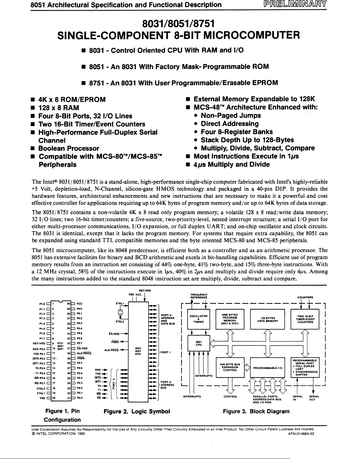
8031/8051/8751
SINGLE-COMPONENT 8-BIT MICROCOMPUTER
•
803t
- Control Oriented CPU With RAM and
I/O
•
8051
- An
8031
With Factory Mask- Programmable ROM
•
8751
-
An
8031
With User Programmable/Erasable EPROM
• 4K x 8 ROM/EPROM
• 128 x 8 RAM
• Four 8-Bit Ports, 32 I/O Lines
• Two 16-Bit Timer/Event Counters
• High-Performance Full-Duplex Serial
Channel
• Boolean Processor
•
Compatible
with
MCS-80™/MCS-85TM
Peripherals
• External
Memory
Expandable
to
128K
• MCS-48™ Architecture Enhanced with:
• Non-Paged Jumps
• Direct Addressing
• Four 8-Register Banks
• Stack Depth
Up
to 128-Bytes
• Multiply, Divide, Subtract, Compare
• Most Instructions Execute
in
111S
•
411s
Multiply
and Divide
The Intel® 8031/8051/8751
is
a stand-alone, high-performance single-chip computer fabricated with Intel's highly-reliable
+5
Volt, depletion-load, N-Channel, silicon-gate HMOS technology and packaged in a 40-pin DIP. It provides the
hardware features, architectural enhancements and new instructions that are necessary to make
it
a powerful and cost
effective controller for applications requiring up to 64K bytes
of
program memory and /
or
up to 64K bytes
of
data
storage.
The
8051/8751 contains a non-volatile 4K x 8 read only program memory; a volatile
128
x 8 read/write data memory;
32
I/O
lines; two 16-bit timer/counters; a five-source, two-priority-Ievel, nested interrupt structure; a serial
I/O
port for
either multi-processor communications,
I/O
expansion,
or
full duplex UART; and on-chip oscillator and clock circuits.
The
8031
is
identical, except that
it
lacks the program memory.
For
systems that require extra capability, the
8051
can
be
expanded using standard TTL compatible memories and the byte oriented MCS-80 and MCS-85 peripherals.
The
8051
microcomputer, like its 8048 predecessor,
is
efficient both as a controller and as an arithmetic processor. The
8051
has extensive facilities for binary and BCD arithmetic and excels in bit-handling capabilities. Efficient
use
of
program
memory results from
an
instruction set consisting
of
44% one-byte,
41%
two-byte, and
15%
three-byte instructions. With
a
12
MHz crystal, 58%
of
the instructions execute in Ills, 40% in
2f1s
and mUltiply and divide require only
411S.
Among
the many instructions added to the standard
8048 instruction set are multiply, divide, subtract and compare.
AST/VPD
FREQUENCY
REFERENCE
COUNTERS
P1.0
vee
P1,1
PO.o
}-.
r
I
I
I
I
I
I
I
I
-1
,...----'---'---,
P1.2
PO.1
P1.3
PO.2
P1.4
PO.3
P1.5
PO.4
P1.6
PO.S
P1.7
PO.S
RST/VPO
PO.7
RXD P3.0
EAtVDO
TXO P3.1
ALEIPROG
INTO P3.2
PSEN
uin
P3.3
P2.7
TO
P3.4
P2.S
T1
P3.5 P2.5
\VA
P3.6
P2."
RD
P3.7
P2.3
XTAL2
P2.2
XTAL1
P2.1
VSS
P2.D
Figure
1.
Pin
Configuration
ADDRESS
AND
OATA
BUS
}-,
PSEN
ALE/PROG
.m_
{{
TXO
.....
INTO
......
INT'......
:
}~"'.
TO-'
g
ADDRESS
n........
Q.
BUS
WA~
AD"-
Figure 2.
Logic
Symbol
I
INTERRUPTS
L-
INTERRUPTS
64K-SYTE
8US
•
EXPANSION
CONTROL
CONTROL
128
BYTES
DATA
MEMORY
PARALLEL
PORTS.
ADDRESS/DATA
BUS,
AND
110
PINS
Figure
3.
Block Diagram
TWO
16-BIT
TIMER/EVENT
COUNTERS
PROGRAMMABLE
SERIAL
PORT
•
FULL
DUPLEX
UART
•
SYNCHRONOUS
SHIFTER
SERIAL SERIAL
IN
OUT
Intel
Corporation
Assumes
No
Responsibility
for
the
Use
of
Any
Circuitry
Other
Than
Circuitry
Embodied
in
an Intel
Product.
No
Other
Circuit
Patent
licenses
Are
Implied.
© INTEL CORPORATION.
1980.
AFN-01488A-02
I
I
I
I
I
I
I
I
I
8051 Single-Chip
Microcomputer
Architectural Specification
and
Functional Description
©Intel Corporation 1980. All rights reserved.
Contents
CHAPTER 1 INTRODUCTION
.....
.-
..
.. .. .. .. .. ..
.... 1
1.0
Abstract. . . . . . . . . . . . . . . . . . . . . . . . . . . . .
..
..
1
1.1
Intel's Complete Line
of
Single-Chip
Microcomputers
........................
1
1.2
Enhancing the 8048 Architecture for
the
80's
................................
1
CHAPTER 2 ARCHITECTURAL OVERVIEW AND
FUNCTIONAL DESCRIPTION
...........
2
2.0
The
8051
Family
........................
2
2.1
Macro-view
of
the
8051
Architecture
......
2
2.1:
1
8051
CPU Architecture . . . . . . . . . . .
..
2
2.1.2
On-Chip Peripheral Functions. . . . .
..
3
2.1.2.1
Interrupt System
..
. . . . . . . .
..
3
2.1.2.2
I/O Facilities. . . . . . . . . . . . . .
..
4
2.1.2.2.1
Open Drain I/O
Pins.
.
..
4
2.1.2.2.2 Quasi-Bidirectional
I/O Pins
...............
4
2.1.2.2.3 Microprocessor Bus
..
..
5
2.1.2.3 Timer/Event Counters
.......
6
2.1.2.4 Serial Communications. . . .
..
7
2.2
CPU Hardware.
..
.
..
.
..
..
..
.
..
.. ..
.
..
...
9
2.2.1
Instruction
Decoder.
. . . . . . . . . . . . .
..
9
2.2.2' Program
Counter
.........
. . . . . . . .
..
9
2.2.3 Internal Data Memory
..............
9
2.2.3.1
Internal Data RAM
...........
9
2.2.3.2 Register Banks
.•...........
9
2.2.3.3 Special Function Registers
...
9
2.2.3.4 A Register. . . . . . . . . . . . . . . .
..
9
2.2.3.5 B Register. . . . . . . . . . . . . . . .
..
9
2.2.3.6
PSW
Register.
.. ..
.. .. ..
....
9
2.2.3.7 Stack Pointer . . . . . . . . . . . . .
..
9
2.2.3.8 Data Pointer
................
11
2.2.4 Arithmetic Section
.................
11
2.2.5
Program Control Section
...........
11
2.2.6
Oscillator and Timing Circuitry
......
11
2.2.7 Boolean Processor
.................
11
2.3
Memory Organization
...................
11
2.4
Operand Addressing
....................
12
2.5
Data Manipulation
...............
"
......
14
2.5.1
Data Transfer Operations
...........
14
2.5.2
logic
Operations
..................
15
2.5.3
Arithmetic Operations
..............
16
2.6
Control Transfer
........................
17
2.7
I nstruction Set
...........................
18
2.7.1
What the Instruction Set Is
...........
18
2.7.2 Organization
of
the Instruction Set
".
18
2.7.3 Operand Addressing Modes and
Associated Operations
.............
21
2.8
Interrupt System
........................
22
2.8.1
External Interrupts
..................
24
2.8.1.1
Transition-Activated
Interrupts
..................
24
2.8.1.2 level-Activated Interrupts
....
24
2.9
Ports and I/O Pins
.......................
24
AFN-Q1488A·03
CHAPTER 2 ARCHITECTURAL OVERVIEW AND
FUNCTIONAL
DESCRIPTION (Continued)
2.10 Accessing External
Memory
..............
25
2.10.1 Operation
of
Ports
................
26
2.10.2 Bus Cycle Timing
.................
26
2.11
TimerlCounter
..........................
28
2.11.1 TIC Mode Selection
...............
28
2.11.2 Configuring the
TIC Input
.........
28
2.11.3 TIC Operation
....................
29
2.11.4 Reading and
Reloading the TIC
....
29
2.12
Serial Channel
..........................
29
2.12.1
Serial Port Control Register and
2.13
2.14
2.15
2.16
2.17
Table
2.1
Serial Data Registers
..........
'
....
31
2.12.2 Operating Modes
.................
31
2.12.2.1 Operating Mode O
•....•••.
31
2.12.2.2 Operating Modes 1
through 3
................
32
2.12.3 The
Serial Frame
.................
32
2.12.4 Transmission Rate Generation
.....
32
2.12.5 UART Message Error Conditions
...
33
External Interface
.......................
33
2.13.1
Processor Reset and
Initialization
......................
33
2.13.2
Power Down Operation
of
Internal RAM
.....................
33
EPROM Programming
....................
34
The
8051
as
an
Evolution of the 8048
......
34
Development System and Software
Support
................................
34
8051
Pin Description
....................
35
Instruction Set Summary
.................
37
AFN-01488A-04
8051
Architectural Specification and Functional Description
1.0 ABSTRACT
The 8031, 8051,
and
8751
are the latest additions to Inters
line
of
single-chip microcomputers. The CPU architec-
ture and on-chip peripheral functions
of
the
8051
are
described in this document. A user familiar with the
MCS-48 family should be able to evaluate and design-in
the
8051
using the information included herein.
A detailed description
of
the
hardware required to
expand the
8051
with more program memory,
data
memory,
I/O,
specialized peripherals and into multi-
processor configurations
is
described in the
8051
Family
User's Manual.
1.1
INTEL'S COMPLETE LINE OF
SINGLE-CHIP MICROCOMPUTERS
In
1976
Intel introduced the 8748 microcomputer. This
marked the first time in history that technology permitted
a complete 8-bit computer
to
be fabricated on a single
silicon die. This single chip can control a limitless variety
of
products ranging from appliances to automobiles to
computer terminals.
Since
1976
Intel has offered products for the full range
of
single-chip microcomputer applications by pushing the
8048's architecture in several directions. The 8049 ran
nearly twice as fast
as
the 8748/8048 while doubling the
amount
of
on-chip program memory and
data
memory.
Applications requiring solely external program memory
were satisfied with the
8035 and 8039. Cost sensitive and
less
I/O
intensive applications incorporated the
8021
which executed a subset
of
the 8048's instruction set
at
a
slower speed. Finally, the
8022 integrated an 8-bit
A/D
converter onto the
8021
die to allow the chip to interface
directly to a world in which most signals are analog.
Figure
I.
I positions these products on a performance
versus die-size curve.
10
9
8
7
iu
il 6
c
~
5
o
...
ffi
4
...
3
2
8022.
8048
•
•
8051
8021.
0~------*X----~~1~.5~X------~2~X------.~2.5X
DIE SIZE
-Based on execution speed, memory size and peripheral functions.
Figure 1.1. Performance Versus Cost
1
Now, thanks to the density
of
HMOS, technology has
once again permitted the
birth
of
a microcomputer with
performance
to
leap into new product areas. The
8051
achieves a
lOX
function/speed improvement over the
8048
by packing 60,000 transistors onto a die 230 mils
square.
The
8051
family addresses the high-end
of
the single-chip
computer market.
It
is
the highest performance micfo-
computer family in the world
and
out-performs all micro-
processors and microcomputers in control oriented
applications.
It
offers an upward compatible growth path
for
8048 users with ten times the power
of
the
8048
as
shown in Table
1.1.
•
4X
Program Memory (4k Bytes)
•
2X
Data Memory (128 Bytes)
•
2X
Register Banks (4
vs.
2)
•
2X
Timers (Two 16-bit Timers)
• New Full-Duplex Serial
I/O
Port
• More
I/O
Pins (32
vs.
27)
• Enhanced MCS-48 Architecture
•
21/2
X
To
10X
Execution Speed
•
1.4X Die Size
Table
1.1:
8051
Functions/Speed/Cost Relative
to
8048
1.2 ENHANCING THE 8048 ARCHITEC-
TURE FOR THE 80's
The goal
of
the
8051
is
to extend the architecture
of
the
industry standard
8048 single-chip microcomputer into
the
80's. This meant increasing the power
of
the 8048's
CPU
as well as increasing the power, variety and quantity
of
on-chip CPU peripherals.
The
8048's CPU architecture
is
ideal for control-oriented
applications demanding a low-cost microcomputer because
of
its hardware simplicity and resulting silicon efficiency.
A
simpleALU
is
used in virtually all operations: arith-
metic, logic,
data
moves, bit testing and I/O. Since all
data
is
moved through the ALU this also simplifies the
internal data path. The
8048's simple addressing methods
of
Register-, Register-Indirect- and Immediate-Address-
ing minimize hardware. The conditional branch logic
simply concatenates
an
immediate value to the upper
bits
of
the program counter to economize on silicon, but
results in page boundaries. The simplicity
of
the table-
look-up circuitry also results in page boundaries. The
user flags and test pins provided for monitoring program
and external status in an efficient manner are limited to
two of each. This architecture, and the choice
of
instruc-
tion encodings that it permits, results
In
1,024 byte
programs
of
unsurpassed byte efficiency.
AFN-01488A-05
8051
Architectural Specification and Functional Description
The silicon economic architecture of the
8048
causes
some inconvenience to the programmer but the relatively
short programs (one or two kilobytes) keep frustration
levels in check. The
8051
challenge
was
to maintain soft-
ware and feature compatibility with the
8048
while
providing a more powerful microcomputer that
is
easier
to program and
use.
This allows a designer currently
using the
8048
to easily upgrade to the
8051
while pro-
tecting
his
investment in algorithm development and the
knowledge he gained by designing with the
8048.
Some of the achievements
of
the
8051
were to extend the
maximum program memory address space to 64K-bytes,
extending on-chip peripheral functions (counters, serial
ports and parallel ports) to satisfy emerging single-chip
applications, and enhancing a paged architecture to
make
it
suitable for the relocatable and re-entrant code
generated
by
modern programming techniques. Op codes
were reassigned to add new high-power operations and to
permit
new
addressing modes which make the old
operations more orthogonal. During this process special
care
was
taken to provide optimum byte efficiency and
maximum execution speed. The
8051
is
typically 20%
more code efficient than the 8049 for programs longer
than
2048
bytes. Efficient use of program memory results
from an instruction set consisting of 44% one-byte,
41
%
two-byte and
15%
three-byte instructions. With a
12
M
Hz
crystal,
58%
of the instructions execute
in
ltis, 40%
in
2;,Is
and multiply and divide require 'only 4tis.
2.0 THE
8051
FAMILY
The
8051
is
a stand-alone high-performance single-chip
computer intended for use
in
sophisticated real-time
applications such as instrumentation, industrial control
and intelligent computer peripherals. It provides the
hardware features, architectural enhancements and new
instructions that make it a powerful and cost effective
controller for applications requiring up to 64K-bytes of
program memory
and/
or
up to 64K-bytes
of
data storage.
A Block Diagram
is
shown in Figure
3.
The
8031
is
a control-oriented
CPU
without on-chip
program memory.
It
can address 64K-bytes
of
external
Program Memory in addition to 64K-bytes
of
External
Data Memory.
For
systems requiring extra capability,
each member of the
8051
family can
be
expanded using
standard memories
and
the byte oriented MCS-80 and
MCS-85 peripherals. The
8051
is
an
8031
with the lower
4K-bytes
of
Program Memory filled with on-chip mask
programmable
ROM while the
8751
has 4K-bytes
ofUV-
light-erasable/ electrically-programmable ROM.
The three pin-compatible versions
of
this component
reduce development problems to a minimum and provide
maximum flexibility. The
8751
is
well
suited for develop-
2
ment, prototyping, low-volume production
and
applica-
tions requiring field updates; the
8051
for low-cost,
high-volume production and the
8031
for applications
desiring the flexibility
of
external Program Memory
which can be easily modified
and
updated in the field.
2.1
MACRO-VIEW OF THE
8051
ARCHI-
TECTURE
On a single die the
8051
microcomputer combines CPU;
non-volatile 4K x 8 read-only program memory; volatile
128
x 8 read/write data memory;
32
I/O
lines; two 16-bit
timer / event counters; a five-source, two-priority-Ievel,
nested interrupt structure; serial
I/O
port for either multi-
processor communications,
I/O
expansion,
or
full duplex
UART; and on-chip oscillator and clock circuits. This
section will provide an overview
of
the
8051
by providing
a high-level description
of
its major elements: the
CPU
architecture and the on-chip functions peripheral to the
CPU. The generic term "8051"
is
also used to refer collec-
tively to the
8031,
8051,
and
8751.
2.1.1
8051
CPU Architecture
The
8051
CPU
manipulates
operands
in
four
memory
spaces. These are the 64K-byte Program Memory, 64K-
byte External
Data
Memory, 384-byte Internal
Data
Memory and 16-bit Program Counter spaces. The Inter-
nal
Data
Memory address space
is
further divided into the
256-byte Internal
Data
RAM
and 128-byte Special
Function Register
(SFR) address spaces shown in Figure
2.1. Four Register Banks (each with eight registers),
128
addressable bits, and the stack reside in the Internal
Data
RAM. The stack depth
is
limited only by the available
Internal Data
RAM
and its location
is
determined by the
8-bit
Stack Pointer.
All
registers except the Program
Counter and the four 8-Register Banks reside in the
Special Function Register address space. These memory
mapped registers include arithmetic registers, pointers,
I/O
ports, and registers for the interrupt system, timers
and serial channel.
128
bit locations in the
SFR
address
space are addressable as bits. The
8051
contains
128
bytes
of Internal Data RAM and
20
SFRs.
The
8051
provides a non-paged Program Memory
address space to accommodate relocatable code.
Con-
ditional branches are performed relative to the Program
Counter. The register-indirect
jump
permits branching
relative to a 16-bit base register with
an
offset provided by
an 8-bit index register. Sixteen-bit jumps and calls permit
branching to any location in the contiguous 64K
Program
Memory address space.
The
8051
has
five
methods for addressing source oper-
ands: Register, Direct, Register-Indirect, Immediate, and
Base-Register- plus Index-Register- Indirect Addressing.
AFN-01488A-06
8051
Architectural Speciffcation ancrFunctionaJ Descrlpfion
t
64K
64K
EXTERNAl-
OYERl-APPED SPACE
I
------
-"Lr-----A
4095
'l
INTERNAl-
255 I I
25S
,
I I
1~1..
I
128
,
-
PROGRAM
COUNTER
0
,
,
PROGRAM
MEMORY
J
,
INTERNAl-
DATA RAM
,
-
,
SPECIAL
FUNCTION
REGISTERS
INTERNAL
DATA MEMORY
,
,
EXTERNAL
DATA
MEMORY
,
Figure 2.1.
8051
Family Memory Organization
The first three methods can
be
used for addressing
destination operands. Most instructions have a
"desti-
nation,source" field that specifies the data type, address-
ing methods
and
operands
involved.
For
operations
other than moves, the destination operand
is
also a source
operand.
Registers
in the four 8-Register Banks can
be
accessed
through Register, Direct,
or
Register-Indirect Ad-
dressing; the
128
bytes of Internal Data RAM through
Direct or Register-Indirect Addressing; and the
Special
Function Registers through Direct Addressing. External
Data Memory
is
accessed through Register-Indirect
Addressing. Look-Up-Tables resident in Program
Memory can
be
accessed through Base-Register- plus
Index-Register- Indirect Addressing.
The
80S
1
is
classified as an 8-bit machine since the
internal
ROM, RAM, Special Function Registers,
Arithmeticl
Logic Unit and external data bus are each
8-
bits wide. The
80S
1 performs operations on bit, nibble,
byte and double-byte data types.
The
80S1
has extensive facilities for byte transfer, logic,
and integer arithmetic operations. It excels
at
bit handling
since data transfer, logic and conditional branch
operations· can be performed directly on Boolean
variables.
The
80S
I's instruction set
is
an
enhancement
of
the
instruction set familiar to
MCS-48 users.
It
is
enhanced to
allow expansion of
on-chip· CPU peripherals and to
optimize byte efficiency and execution speed.
Op codes
were reassigned to add new high-power operations and to
permit
new
addressing modes which make the old
operations more orthogonal. Efficient use
of
program
memory results from an instruction set consisting of
49
3
single-byte,
4S
two-byte and
17
three-byte instructions.
When using a
12
MHz oscillator, 64 instructions execute
in
IlJs
and
4S
instructions execute in
4ls.
The remaining
instructions (multiply and divide) require only
~s.
The
number of bytes
in
each instruction and the number
of
oscillator periods required for execution are listed in the
appended
80S
I Instruction Set Summary.
2.1.2 On-Chip Peripheral Functions
Thus
far
only
the
CPU
and
memory
spaces
of
the
80S 1
have been described. In addition to the CPU and
memories, an interrupt system, extensive
I/O
facilities,
and several peripheral functions are integrated on-chipto
relieve the CPU
of
repetitious, complicated
or
time-
critical tasks and to permit stringent real-time control
of
external system interfaces. The extensive 110 facilities
include the
110 pins, parallel 110 ports, bidirectional
address/data bus and the serial port for
I/O
expansion.
The CPU peripheral functions integrated on-chip are the
two 16-bit counters and the serial port. All
of
these work
together to greatly boost system performance.
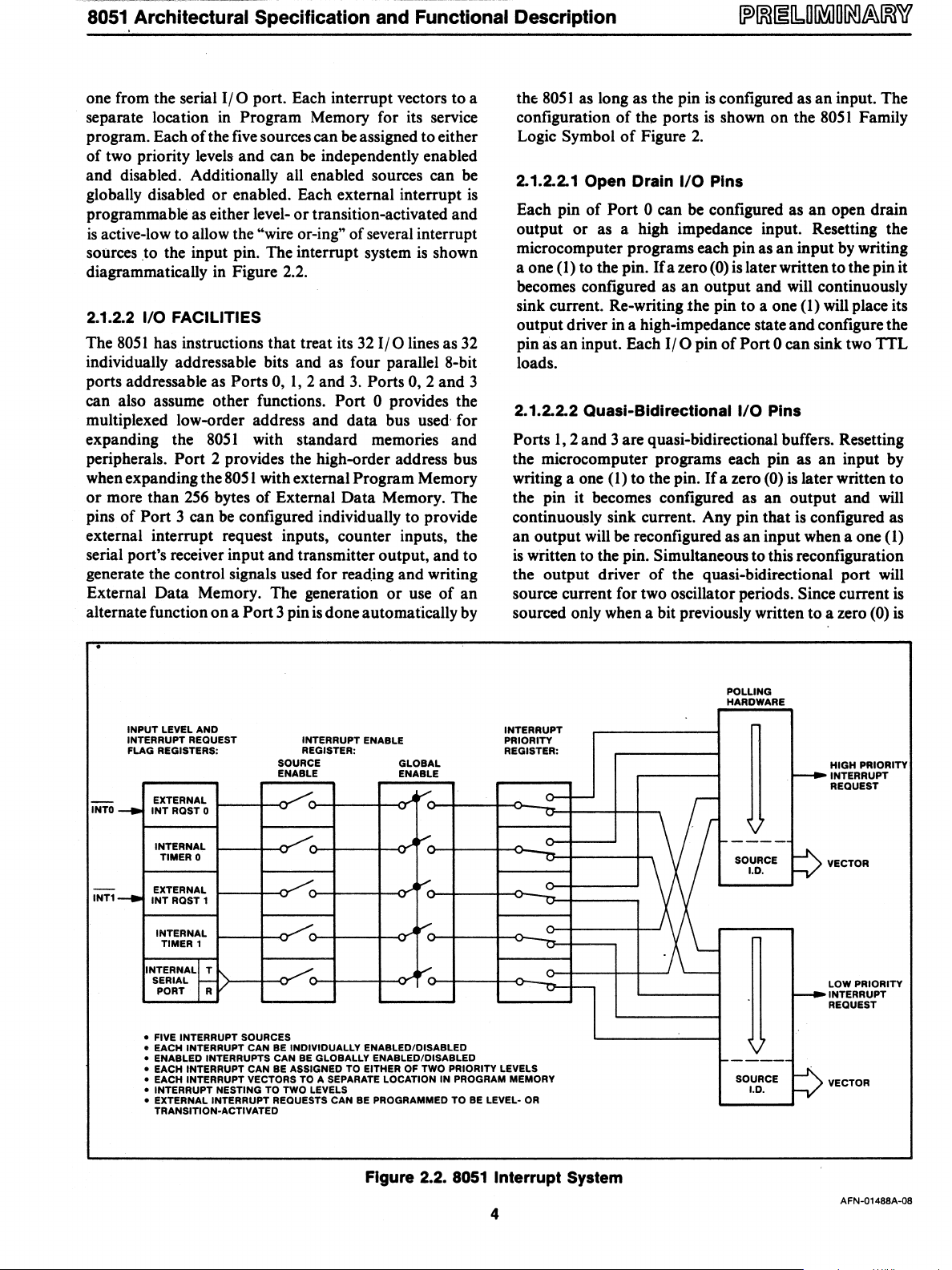
2.1.2.1
INTERRUPT SYSTEM
External events and the
real~time-driven
on-chip
peripherals require service by the CPU asynchronous to
the execution
of
any particular section
of
code.
To
tie the
asynchronous activities of these functions to normal
program execution, a sophisticated multiple-source,
two~
priority-level, nested interrupt system
is
provided. In-
terrupt response latency ranges from
3IJs
to
7IJs
when
using a
12
MHz crystal.
The
80S
I acknowledges interrupt requests from
five
sources:
Two
from external sour.res
via
the
INTO
and
INTI pins, one from each
of
the two internal counters and
AFN-Ol488A-D7
8051
Architectural Specification and Functional Description
one from the serial
I/O
port. Each interrupt vectors to a
separate location
in
Program Memory for its service
program. Each
of
the
five
sources can
be
assigned to either
of two priority levels and can
be
independently enabled
and disabled. Additionally all enabled sources can
be
globally disabled
or
enabled. Each external interrupt
is
programmable as either level-
or
transition-activated and
is
active-low to allow the "wire or-ing" of several interrupt
sources
.to
the input pin. The interrupt system
is
shown
diagrammatically in Figure 2.2.
2.1.2.2 1/0 FACILITIES
The
8051
has instructions that treat its
32
I/O
lines as
32
individually addressable bits and as four parallel 8-bit
ports addressable as
Ports 0,
1,2
and
3.
Ports
0,2
and 3
can also assume other functions.
Port 0 provides the
multiplexed low-order address and data bus
used,
for
expanding the
8051
with standard memories and
peripherals.
Port 2 provides the high-order address bus
when expanding the
8051
with external Program Memory
or
more than
256
bytes
of
External Data Memory. The
pins of
Port 3 can
be
configured individually to provide
external interrupt request inputs, counter inputs, the
serial port's receiver input and transmitter output, and to
generate the control signals used for reading and writing
External Data Memory. The generation
or
use
of
an
alternate function
on
a Port 3 pin
is
done automatically by
INPUT LEVEL AND
INTERRUPT
REQUEST INTERRUPT ENABLE
FLAG
REGISTERS:
REGISTER:
SOURCE
GLOBAL
ENABLE
ENABLE
eXTERNAL
..AI'"
INTO
......
INTRQST0
INTERNAL
.....
...AI"'"
TIMER 0
I"'"
EXTERNAL
......
INT
RQST 1
-
tNT1
INTERNAL
I'"
TIMER 1
INTERNAL~
r:.
SERIAL
,..
PORT R
• FIVE INTERRUPT SOURCES
•
EACH INTERRUPT CAN BE INDIVIDUALLY ENABLED/DISABLED
•
ENABLED INTERRUPTS CAN BE GLOBALLY ENABLED/DISABLED
the
8051
as
long as the pin is configured as an input. The
configuration
of
the ports is shown
on
the
8051
Family
Logic
Symbol
of
Figure
2.
2.1.2.2.1 Open Drain 1/0 Pins
Each pin
of
Port 0 can be configured as
an
open drain
output
or
as a high impedance input. Resetting the
microcomputer programs each pin as
an
input
by
writing
a one (I) to the pin.
Ifa
zero
(0)
is later written to the pin it
becomes configured as
an
output and will continuously
sink current. Re-writing the pin to a one (I) will place its
output driver in a high-impedance state and configure the
pin
as
an
input. Each
I/O
pin
of
Port 0 can sink two TTL
loads.
2.1.2.2.2 Quasi-Bidirectional
1/0
Pins
Ports
1,2
and 3 are quasi-bidirectional buffers. Resetting
the microcomputer programs each pin as
an
input by
writing a one
(l)
to the pin. If a zero (0)
is
later written to
the pin it becomes configured as an output and
will
continuously sink current. Any pin that is configured as
an
output will
be
reconfigured as
an
input when a one (I)
is
written to the pin. Simultaneous to this reconfiguration
the output driver
of
the quasi-bidirectional port
will
source current for two oscillator periods. Since current
is
sourced only when a bit previously written to a zero
(0)
is
INTERRUPT
PRIORITY
REGISTER:
-
POLLING
HARDWARE
V
1-----
SOURCE
I.D.
V
-----
------
=>
r--
HIGH PRIORITY
INTERRUPT
REQUEST
VECTOR
LOW PRIORITY
INTERRUPT
REQUEST
•
EACH INTERRUPT CAN BE ASSIGNED TO EITHER OF TWO PRIORITY LEVELS
~
• EACH INTERRUPT VECTORS TO A SEPARATE LOCATION IN PROGRAM MEMORY
SOURCE
•
INTERRUPT NESTING TO TWO LEVELS
I.D.
VECTOR
•
EXTERNAL INTERRUPT REQUESTS CAN BE PROGRAMMED
TO
BE LEVEL-
OR
TRANSITION-ACTIVATED
Figure 2.2. 8051
Interrupt
System
AFN-01488A-08
4
8051
Architectural Specification and Functional Description
updated to a one (1), a pin programmed as
an
input will
not
source current into the
TTL
gate
that
is driving
it
if
the
pin is
later written with
another
one (1). Since
the
quasi-
bidirectional
output
driver sources current for only two
oscillator periods,
an
internal pullup resistor
of
ap-
proximately 20K- to 4OK-ohms
is
provided to hold the
external
driver's loading
at
a
TTL
high level. Ports
1,
2
and
3 can sink/ source one TTL load.
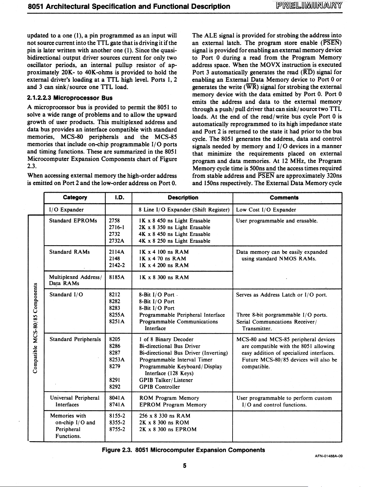
2.1.2.2.3
Microprocessor
Bus
A microprocessor bus is provided to permit the
80S
1
to
solve a wide range
of
problems
and
to allow the upward
growth
of
user products. This multiplexed address
and
data
bus provides
an
interface compatible with standard
memories,
MCS-80 peripherals
and
the MCS-8S
memories
that
include on-chip programmable
I/O
ports
and
timing functions. These are summarized in the
80S
1
Microcomputer Expansion Components
chart
of
Figure
2.3.
When accessing external memory the high-order address
is
emitted
on
Port
2
and
the low-order address
on
Port
O.
The ALE signal is provided
for
strobing the address into
an
external latch.
The
program store enable (PSEN)
signal is provided for enabling
an
external memory device
to
Port
0 during a read from the Program Memory
address space. When the
MOVX instruction is executed
Port
3 automatically generates the read
(RD)
signal
for
enabling
an
External
Data
Memory device
to
Port
0
or
generates the write
(WR)
signal for strobing the external
memory device with the
data
emitted by
Port
O.
Port
0
emits the address
and
data
to
the external memory
through a push/ pull driver
that
can sink/ source two
TTL
loads. At the end
of
the read/write bus cycle
Port
0 is
automatically reprogrammed
to
its high impedance state
and
Port
2 is returned
to
the state it had
prior
to
the bus
cycle. The
80S
1 generates the address,
data
and
control
signals needed by memory
and
I/O
devices in a manner
that
minimize the requirements placed
on
external
program and
data
memories.
At
12
MHz, the Program
Memory cycle time is
SOOns
and
the access times required
from stable address
and
PSEN
are
approximately 320ns
and
lSOns
respectively. The External
Data
Memory cycle
Category
1.0.
Description
Comments
I/O
Expander
8 Line
I/O
Expander (Shift Register)
Low Cost
I/O
Expander
Standard
EPROMs
2758 I K x 8 450 ns Light Erasable
User programmable
and
erasable.
2716-1 2K x 8 350 ns Light Erasable
2732
4K x 8 450 ns Light Erasable
2732A
4K
x 8 250 ns Light Erasable
Standard
RAMs 2114A
IK
x 4
100
ns
RAM
Data
memory can be easily expanded
2148
lK
x 4 70 ns
RAM
using standard
NMOS
RAMs.
2142-2
I K x 4
200 ns
RAM
Multiplexed Address/
8185A
I K x 8
300
ns
RAM
'"
Da.ta
RAMs
C
'"
Standard
I/O
8-Bit Ii 0
Port
.
c
8212
Serves as Address Latch
or
I/O
port.
0
Q,
8282
8-Bit
I/O
Port
e
0
8283
8-Bit
I/O
Port
U
on
8255A Programmable Peripheral Interface Three 8-bit porgrammable
I/O
ports.
QO
8251
A
Programmable Communications
Serial Communcations Receiver/
Q
QO
Interface
Transmitter .
•
ell
U
Standard
Peripherals 8205
I
of
8 Binary Decoder MCS-80 and MCS-85 peripheral devices
~
'"
8286
Bi-directional Bus Driver are compatible with the
8051·
allowing
;§
8287
Bi-directional Bus Driver (Inverting) easy addition
of
specialized interfaces.
;
Q,
8253A
Programmable Interval Timer
Future
MCS-80/85 devices will also be
e
8279
Programmable Keyboard/ Display compatible.
0
U
Interface (128 Keys)
8291
GPIB
Talker/Listener
8292
GPIB Controller
Universal Peripheral
8041
A
ROM
Program
Memory User programmable to perform custom
Interfaces 8741A
EPROM
Program
Memory
I/O
and control functions.
Memories with
8155-2
256 x 8 330 ns
RAM
on-chip
I/O
and
8355-2 2K x 8 300 ns ROM
Peripheral 8755-2
2K x 8
300 ns
EPROM
Functions.
Figure 2.3.
8051
Microcomputer Expansion Components
AFN-Q1488A-09
5
8051
Architectural Specification and Functional Description
time
is
IllS
and the access times required from stable
address and from read (RD) or write (WR) command are
approximately 600ns and 250ns respectively.
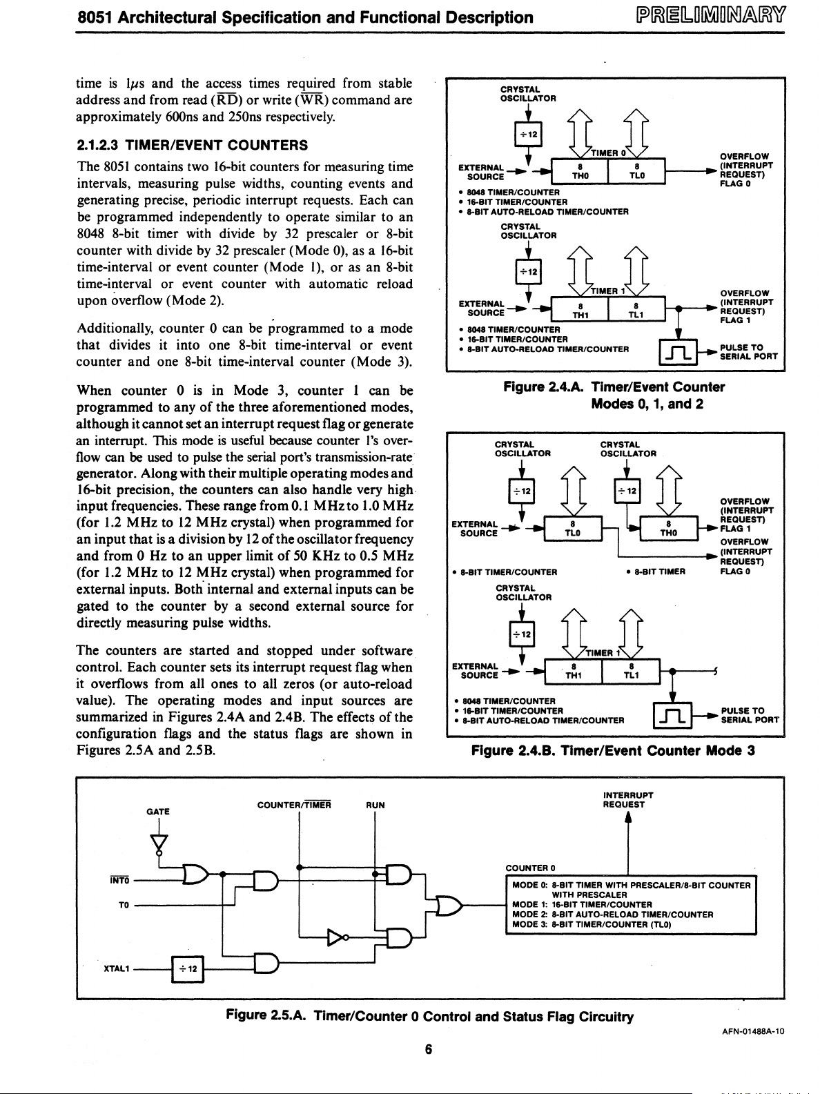
2.1.2.3 TIMER/EVENT COUNTERS
The
8051
contains two 16-bit counters for measuring time
intervals, measuring pulse widths, counting events and
generating precise, periodic interrupt requests. Each can
be programmed independently to operate similar to an
8048
8-bit timer with divide
by
32
prescaler or 8-bit
counter with divide by
32
prescaler (Mode 0), as a 16-bit
time-interval or event counter (Mode I), or
as
an 8-bit
time-interval or event counter with automatic reload
upon overflow (Mode
2).
Additionally, counter 0 can be programmed to a mode
that divides it into one 8-bit time-interval
or
event
counter and one 8-bit time-interval counter (Mode
3).
When counter 0
is
in Mode
3,
counter I can be
programmed to any
of
the three aforementioned modes,
although it cannot set an interrupt request flag
or
generate
an interrupt. This mode
is
useful
because counter
I's
over-
flow
can be
used
to pulse the serial port's transmission-rate
generator. Along with their multiple operating modes and
16-bit precision, the counters can also handle very high
input frequencies. These range from
0.1
MHzto
1.0
MHz
(for
1.2
MHz to
12
MHz
crystal) when programmed for
an input that
is
a division by
12
of the oscillator frequency
and from
0 Hz to an upper limit
of
50
KHz to 0.5 MHz
(for
1.2
MHz to
12
MHz crystal) when programmed for
external inputs.
Both· internal and external inputs can be
gated to the counter by a second external source for
directly measuring pulse widths.
The counters are started and stopped under software
control. Each counter sets its interrupt request flag when
it overflows from all ones to
aU
zeros (or auto-reload
value). The operating modes and input sources are
summarized
in Figures 2.4A and 2.4B. The effects
of
the
configuration flags and the status flags are shown in
Figures 2.5A and 2.5B.
GATE
COUNTER/TIMER RUN
INTO
--~=-~l:'~>-"t"--r-\--J====j~:J
TO------~
XTAl1
CRYSTAL
OSCILLATOR
$
EXTERNAL-.
SOURCE
•
8048 TIMER/COUNTER
• 16-BIT TIMER/COUNTER
• 8-BIT AUTO-RELOAD
TIMER/COUNTER
CRYSTAL
OVERFLOW
~_--I~
(INTERRUPT
REQUEST)
FLAG 0
OVERFLOW
°ii~O,.R
__
~~~~~
__
~
EXTSOEURRNCALE
-.
1---4t----I~
(INTERRUPT
REQUEST)
•
8048 TIMER/COUNTER
• 16-BIT TIMER/COUNTER
• 8-BIT AUTO-RELOAD TIMER/COUNTER
FLAG 1
PULSE TO
SERIAL PORT
Figure 2.4.A. Timer/Event Counter
Modes
0,
1,
and 2
CRYSTAL
OSCilLATOR
$
EXTERNAL
___
SOURCE
CRYSTAL
OSCILLATOR
OVERFLOW
(INTERRUPT
REQUEST)
FLAG
1
OVERFLOW
L--
____
--I~ (INTERRUPT
REQUEST)
FLAG 0
• 8-BIT TIMER/COUNTER
CRYSTAL
OSCilLATOR
$
EX;5~:~~'"
• 8048 TIMER/COUNTER
• 16-BIT TIMER/COUNTER
• 8-BIT AUTO-RELOAD TIMER/COUNTER
• 8-BIT
TIMER
PULSE TO
SERIAL PORT
Figure 2.4.8. Timer/Event Counter Mode 3
COUNTER 0
INTERRUPT
REQUEST
MODE
0:
8-BIT TIMER WITH PRESCALER/8-BIT COUNTER
WITH PRESCAlER
>----f
MODE
1:
16-BIT TIMER/COUNTER
MODE
2:
8-BIT AUTO-RELOAD TIMER/COUNTER
MODE
3:
8-BIT TIMER/COUNTER (TlO)
Figure
2.S.A.
Timer/Counter 0 Control and Status Flag Circuitry
AFN-01488A-l0
6
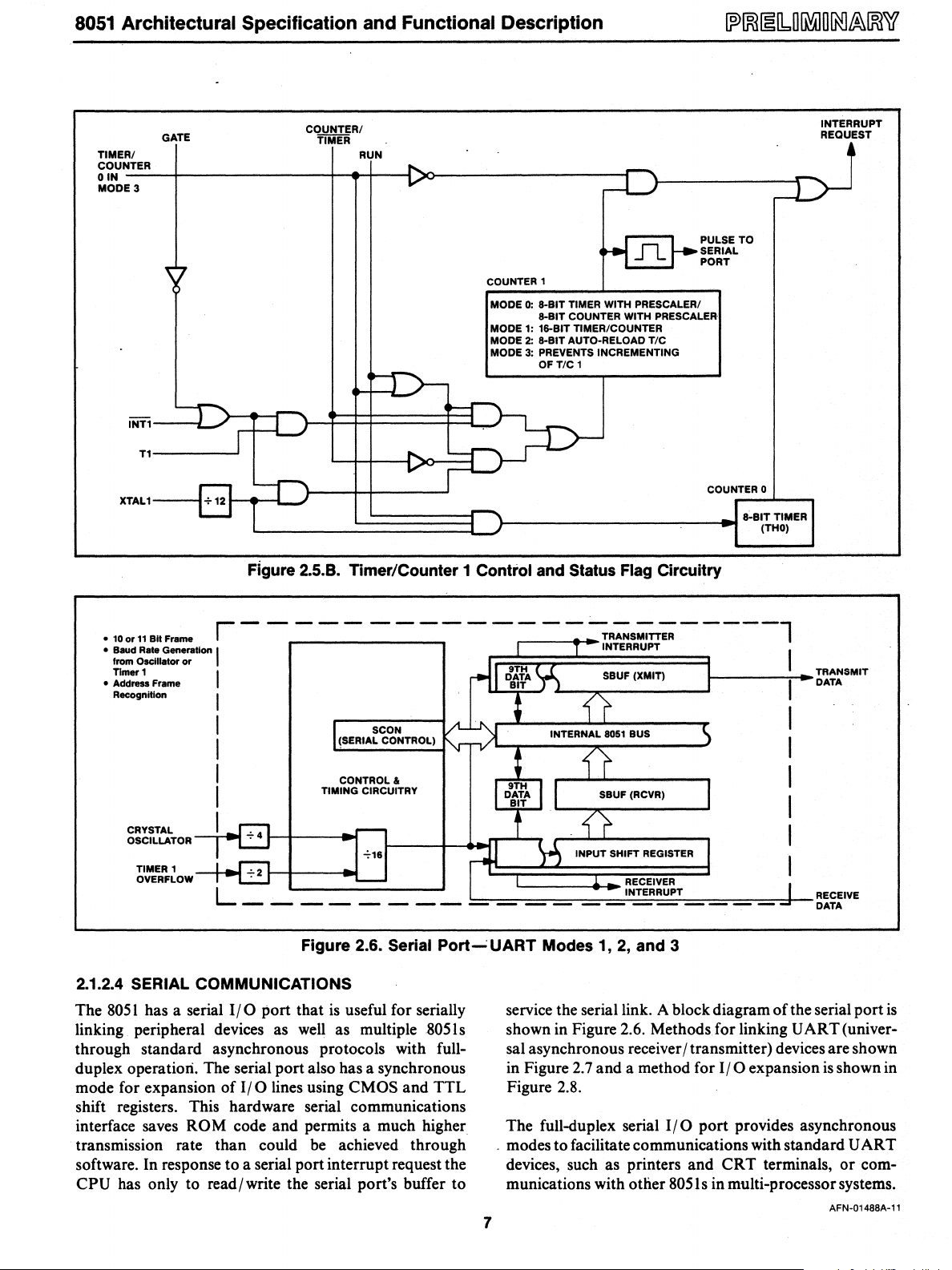
8051
Architectural Specification and Functional Description
COUNTERI
INTERRUPT
GATE
TIMER
REQUEST
TIMERI
RUN
•
COUNTER
~
OIN
-
MODE 3
G
J
)-
Hn
PULSE
TO
SERIAL
PORT
COUNTER 1
MODE
0:
8-BIT TIMER WITH PRESCALERI
8-BIT COUNTER WITH PRESCALER-
MODE
1: 16-BIT TIMER/COUNTER
MODE 2: 8-BIT AUTO-RELOAD TIC
MODE
3:
PREVENTS INCREMENTING
OF TIC 1
J
>-
--
1"'"
~
r-r-
INT1
:=fJ-
T1
~r~
-r-
-
-
1
"'
COUNTER 0
XTAL1
+12
~
-
~
8-8ITTIMER
~
(THO)
Figure 2.5.8. Timer/Counter 1 Control and Status Flag Circuitry
• 100r11
Bit
Frame r - - -
--
- -
--
-
--
-
---:;:R:;:;S;.-TT-;;-----l
• Baud
Rate
Generetlon I INTERRUPT
from Oscillator
or
Timer 1 I
• Address Frame
Recognition I
I
I
I
I
g:~~~~t.,.OR
-
....
1 .....
TIMER 1
SCON
(SERIAL CONTROL)
CONTROL"
TIMING CIRCUITRY
-:-16
I-
___
-:-
__
~~~~SMIT
~-~-----~
OVERFLOW
RECEIVER
L
______________
~~
___
_
RECEIVE
DATA
Figure 2.6. Serial
Port~UART
Modes 1, 2, and 3
2.1.2.4 SERIAL COMMUNICATIONS
The
8051
has a serial
I/O
port that
is
useful for serially
linking peripheral devices as
well
as
multiple805ls
through standard asynchronous protocols with full-
duplex operatiori. The serial port also has a synchronous
mode for expansion of
I/O
lines using CMOS and TTL
shift registers. This hardware serial communications
interface saves
ROM code and permits a much higher
transmission rate than could be achieved through
software. In response
to
a serial port interrupt request the
CPU has only to read/write the serial port's buffer to
7
service the serial link. A block diagram
of
the serial port
is
shown in Figure 2.6. Methods for linking U
ART
(univer-
sal asynchronous receiver / transmitter) devices are shown
in Figure
2.7
and a method for
I/O
expansion
is
shown in
Figure 2.8.
The full-duplex serial
I/O
port provides asynchronous
o modes to facilitate communications with standard U
ART
devices, such as printers and
CRT
terminals, or com-
munications with other
8051s in multi-processor systems.
AFN-01488A-11
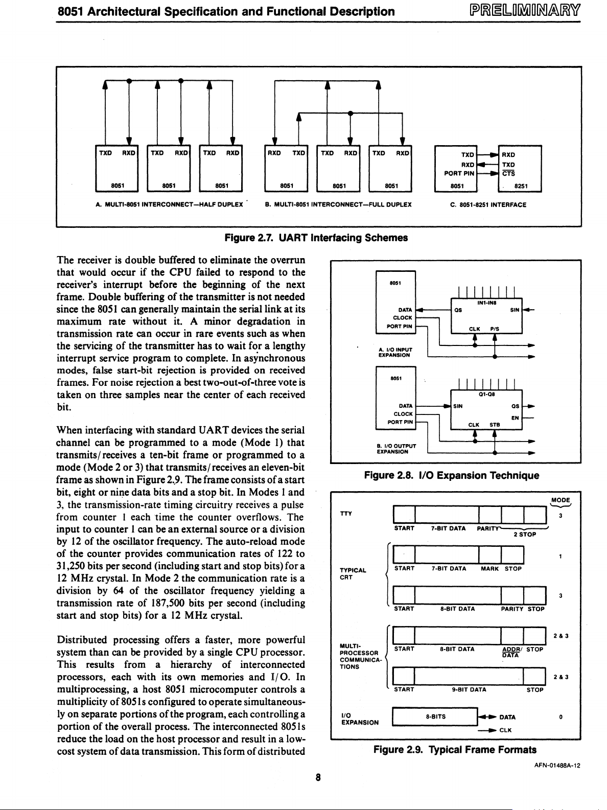
8051 Architectural Specification and Functional Description
I
.~
~
I
TXD RXD
TXD RXD TXD
RXD
RXD TXD
TXD
RXD TXD RXD
TXD
r-----
RXD
RXD
~.
TXD
PORT PIN
CTS
8051 8051
8051 8051
8051
8051
8051
8251
A. MULTI-80S1
INTERCONNECT
-HALF
DUPLEX B. MULTI-80S1
INTERCONNECT
-FULL
DUPLEX
C.
8051-8251 INTERFACE
Figure 2.7.
UART
Interfacing Schemes
The receiver
is
double buffered to eliminate the overrun
that would occur if the
CPU
failed to respond to the
receiver's interrupt before the beginning
of
the next
frame. Double buffering
of
the transmitter is not needed
since the
8051
can generally maintain the serial link
at
its
maximum rate without it. A minor degradation in
transmission rate can occur in rare events such as when
the servicing
of
the transmitter has to wait for a lengthy
interrupt service program to complete. In asynchronous
modes, false start-bit rejection
is
provided on received
frames.
For
noise rejection a best two-out-of-three vote
is
taken on three samples near the center
of
each received
bit.
When interfacing with standard UART devices the serial
channel can be programmed to a mode (Mode
1)
that
transmits/ receives a ten-bit frame
or
programmed
to
a
mode (Mode 2
or
3)
that transmits/receives an eleven-bit
frame as shown in Figure 2
..
9.
The frame consists
of
a start
bit, eight
or
nine data bits and a stop bit. In Modes 1 and
3,
the transmission-rate timing circuitry receives a pulse
from counter
I each time the counter overflows. The
input to counter 1 can
be
an
external source
or
a division
by
12
of the oscillator frequency. The auto-reload mode
of
the counter provides communication rates
of
122
to
31,250 bits per second (including start and stop bits) for a
12
MHz crystal. In Mode 2 the communication rate
is
a
division by 64
of
the oscillator frequency yielding a
transmission rate of
187,500 bits per second (including
start and stop bits) for a
12
MHz crystal.
Distributed processing offers a faster, more powerful
system than can
be
provided by a single
CPU
processor.
This results from a hierarchy
of
interconnected
processors, each with its own memories and
1/
O.
In
multiprocessing, a host
8051
microcomputer controls a
multiplicity
of
8051
s configured to operate simultaneous-
lyon
separate portions
of
the program, each controlling a
portion
of
the overall process. The interconnected
8051
s
reduce the load on the host processor and result in a
low-
cost system
of
data transmission. This form
of
distributed
8
8051
DATA
CLOCK
PORT
PIN
A.1I0INPUT
EXPANSION
8051
DATA
CLOCK
PORT
PIN
B.
110
OUTPUT
EXPANSION
OS
EN
Figure 2.8. I/O Expansion Technique
TTY
MODE
~~~--------~--~--~---'I~
TYPICAL
CRT
MULTI-
PROCESSOR
COMMUNICA-
TIONS
1/0
EXPANSION
START
7-BIT
DATA
PARITY'
2
STOP
START
7·BIT
DATA MARK STOP
START 8-BIT
DATA
PARITY
STOP
START
a-BIT DATA
~~~:I
STOP
START
9-BIT DATA
STOP
j..DATA
....
------------'
__
ClK
a·BITS
Figure 2.9. Typical Frame Formats
,
2&3
2&3
o
AFN-01488A-12
8051
Architectural Specification and Functional Description
processing
is
especially effective in systems where controls
in a complex process are required
at
physically separated
locations.
In Modes 2
and
3 the automatic wake-up of slave
processors through interrupt driven address-frame
recognition
is
provided
to
facilitate interprocessor com-
munications. The protocol for interprocessor com-
munications
is
shown in Figure 2.10.
1.
Slaves
-Configure
serial
port
to
interrupt
CPU
if the
received ninth
data
bit
is
a one (I).
2.
Master-Transmit
frame containing address in first 8
data
bits
and
set ninth
data
bit (i.e., ninth
data
bit designates address frame).
3.
Slaves - Serial port interrupts
CPU
when address
frame
is
received. Interrupt service program
compares received address to its address.
The slave which has been addressed recon-
figures its serial
port
to interrupt the
CPU
on
all subsequent transmissions.
4.
Master-Transmit
control frames and
data
frames
(these will
be
accepted only by the previously
addressed slave.)
Figure 2.10. Protocol for Multi-Processor
Communications
In synchronous mode (Mode
0)
the high-speed serial port
provides
an
efficient, low-cost method
of
expanding
I/O
lines using standard
TTL
and CMOS shift registers. The
serial channel provides a clock output for synchronizing
. the shifting
of
bits
to/from
an
external register. The
data
rate
is
a.division
by
12
of the oscillator frequency
and
is
I M bits
p(:r
second
at
12
MHz.
2.2 CPU HARDWARE
This section describes the hardware architecture of the
8051's
CPU
in
detaiL The interrupt system and on-chip
functions peripheral to the
CPU are described
in
subsequent sections. A detailed
8051
Functional Block
Diagram
is
displayed in Figure
2.
II.
2.2.1
Instruction Decoder
Each program instruction
is
decoded by the instruction
decoder. This unit generates the internal signals that
control the functions of each unit within the
CPU sec-
tion. These signals control the sources and destination
of data, as
well
as the function of the Arithmetic/Logic
Unit (ALU).
2.2.2 Program Counter
The I6-bit Program Counter (PC) controls the sequence in
which the instructions stored in program memory are
executed.
It
is
manipulated with the Control Transfer
instructions listed in section 2.7.2.
9
2.2.3 Internal Data Memory
The
8051
contains a I 28-byte Internal
Data
RAM
(which
includes registers
R7-RO
in e'ach of four Banks), and
twenty memory-mapped
Special Functional Registers.
2.2.3.1 INTERNAL
DATA
RAM
The Internal
Data
RAM provides a convenient 128-byte
scratch pad memory.
2.2.3.2 REGISTER BANKS
There are four 8-Register Banks within the Internal Data
RAM, each containing registers
R7-RO.
2.2.3.3 SPECIAL
FUNCTION
REGISTERS
The Special Function Registers include arithmetic registers
(A ,
B,
PSW), pointers (SP,
DPH,
DPL) and registers
that provide
an
interface between the CPU and the
on-chip peripheral functions.
2.2.3.4 A REGISTER
The A register
is
the accumulator register. ACC
is
the
location
of
the accumulator in the Internal Data Memory.
2.2.3.5 B REGISTER
The B register
is
dedicated during multiply and divide and
serves as both a source and a destination. During all other
operations the B register
is
simply another location of
the Internal Data Memory.
2.2.3.6 PSW REGISTER
The carry (CY), auxialiary carry (AC), user flag 0 (FO),
register bank select I (RS I), register bank select 0 (RSO),
overflow (OV) and parity (P) flags reside in the Program
Status Word (PSW) Register. These flags are bit-
memory-mapped within the byte-memory-mapped
PSW.
The PSW flags record processor status information and
control the operation of the processor.
The CY, AC, and
OV
flags generally reflect the status of
the latest arithmetic operation. The P flag
always reflects
the parity of the A register. The carry flag
is
also a
Boolean accumulator for bit operations.
Specific details
are provided in the
"Flag Register Settings" section
of
2.7.2.
FO
is
a general purpose flag which
is
pushed onto the
stack as
part
of
a PSW save.
The two Register Bank select bits
(RS I 'and
RSO)
deter-
mine which of the four 8-Register Banks
is
selected.
2.2.3.7 STACK POINTER
The 8-bit Stack Pointer (SP) contains the address at
which the last byte
was
pushed onto the stack. This
is
also the address of the next byte that
will
be
popped.
SP
is
updatable under software control.
AFN·01488A-13
 Loading...