

Page 1
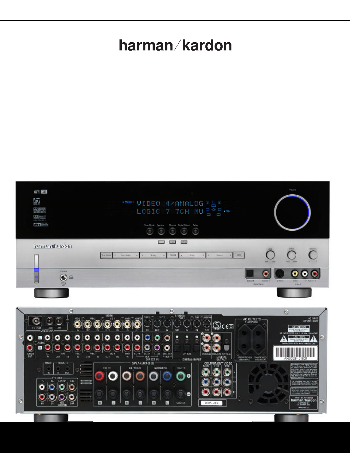
AVR 335
Power for the Digital Revolution
.
®
®
AUDIO/VIDEO RECEIVER
SERVICE MANUAL
Page 2
Technical Specifications
Audio Section
Stereo Mode
Continuous Average Power (FTC)
70 Watts per channel, 20Hz–20kHz,
@ < 0.07% THD, both channels driven into 8 ohms
5/7 Channel Surround Modes
Power Per Individual Channel
Front L&R channels:
55 Watts per channel,
@ < 0.07% THD, 20Hz–20kHz into 8 ohms
Center channel:
55 Watts, @ < 0.07% THD, 20Hz–20kHz into 8 ohms
Surround (L & R Side, L & R Back) channels:
55 Watts per channel,
@ < 0.07% THD, 20Hz–20kHz into 8 ohms
Input Sensitivity/Impedance
Linear (High Level) 200mV/47kohms
Signal-to-Noise Ratio (IHF-A) 95dB
Surround System Adjacent Channel Separation
Analog Decoding 40dB
(Pro Logic, etc.)
Dolby Digital (AC-3) 55dB
DTS 55dB
FM Tuner Section
Frequency Range 87.5–108MHz
Usable Sensitivity IHF 1.3 µV/13.2dBf
Signal-to-Noise Ratio Mono/Stereo: 70/68dB (DIN)
Distortion Mono/Stereo: 0.2/0.3%
Stereo Separation 40dB @ 1kHz
Selectivity ±400kHz: 70dB
Image Rejection 80dB
IF Rejection 90dB
AM Tuner Section
Frequency Range 522–1611kHz
Signal-to-Noise Ratio 45dB
Usable Sensitivity Loop: 500µV
Distortion 1kHz, 50% Mod: 0.8%
Selectivity ±10kHz: 30dB
Video Section
Video Format PAL/NTSC
Input Level/Impedance 1Vp-p/75 ohms
Output Level/Impedance 1Vp-p/75 ohms
Video Frequency Response
(Composite and S-Video) 10Hz–8MHz (-3dB)
Video Frequency
Response (Component) 10Hz-50MHz (-3dB)
Frequency Response
@ 1W (+0dB, –3dB) 10Hz–100kHz
High Instantaneous
Current Capability (HCC) ±35 Amps
Transient Intermodulation
Distortion (TIM) Unmeasurable
Rise Time 16 µsec
Slew Rate 40V/µsec**
Supplied Accessories
The following accessory items are supplied with the AVR 335. If any of
these items are missing, please contact Harman Kardon customer
service at www.harmankardon.com.
• A system remote control • An AM loop antenna
• A Zone II remote control • An FM wire antenna
• The EzSet+ microphone • Five AAA batteries
with a plug adaptor
at the end of the unit’s cord
General
Power Requirement AC 220-240V/ 50Hz
Power Consumption 118W idle, 890W maximum
(7 channels driven)
Dimensions (Max)
Width 440mm
Height 165mm
Depth 382mm
Weight 14.1 kg
Depth measurement includes knobs, buttons and terminal connections.
Height measurement includes feet and chassis.
All features and specifications are subject to change without notice.
Harman Kardon is a registered trademark, and Power for the digital revolution is a trademark, of
Harman International Industries, Inc.
is a trademark of Harman International Industries, Inc.
*Manufactured under license from Dolby Laboratories.
“Dolby,”“Pro Logic,” “Pro Logic II” and the Double-D symbol are
trademarks of Dolby Laboratories. Confidential Unpublished
Works. ©1992–1999 Dolby Laboratories, Inc. All rights reserved.
DTS and DTS Surround, DTS-ES and DTS Neo:6 are trademarks of Digital Theater Systems, Inc.
VMAx is a trademark of Harman International Industries, Inc.,and is an
implementation of Cooper Bauck Transaural Stereo under patent license.
Logic 7 is a registered trademark of Harman International Industries, Incorporated.
**Without input anti slewing and output isolation networks.
TECHNICAL SPECIFICATIONS
Page 3
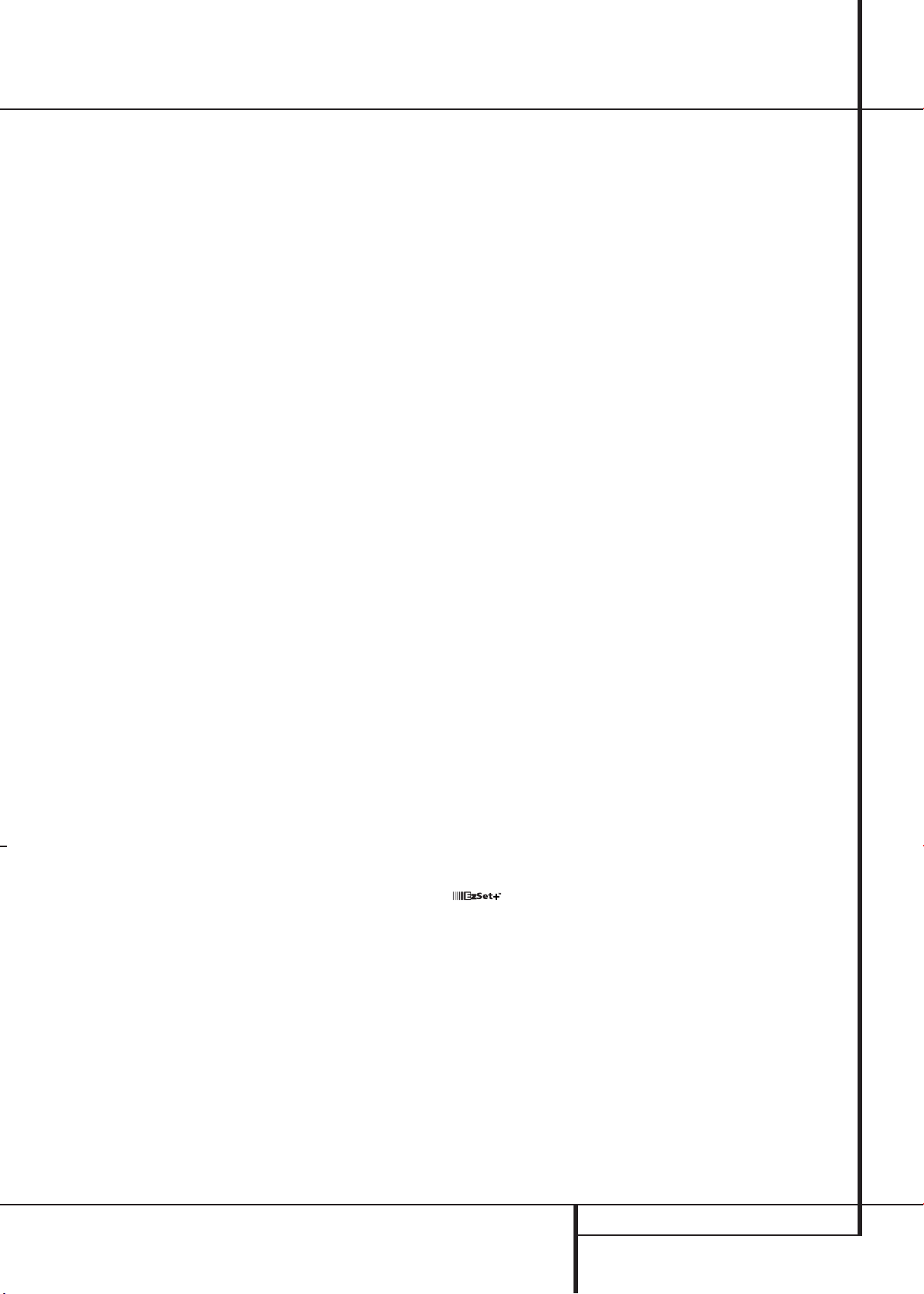
Front Panel Controls
Set up
MIC
2
4
8
6
5
)
!
@
%
*
Ô
Ò
1
3
9 7 #
^
Ù
(
˜
ˆ
&
¯
Ú
ı
Ó
7
$
Û
Main Power Switch
1
System Power Control
2
Power Indicator
3
Headphone Jack
4
Surround Mode Group Selector
5
Speaker Select Button
6
Selector Buttons
7
Tone Mode
8
Surround Mode Selector
9
Tuning
)
1
Main Power Switch: Press this button to
apply power to the AVR. When the switch is
pressed in, the unit is placed in a Standby
mode, as indicated by the orange LED
button MUST be pressed in to operate the unit.
To turn the unit off completely and prevent the
use of the remote control, this switch should be
pressed until it pops out from the front panel so
that the word “OFF” may be read at the top of
the switch.
NOTE: This switch is normally left in the “ON”
position.
3
. This
Tuner Band Selector
!
Set Button
@
Preset Stations Selector
#
Speaker/Channel Input Indicator
$
Input Source Selector
%
RDS Select Button
^
Delay
&
Digital Optical 3 Input
*
Surround Mode Indicators
(
Digital Coax 3 Input
Ó
2
System Power Control: When the Main
Power Switch
turn on the AVR; press it again to turn the unit
off (to Standby). Note that the Power Indicator
3
will turn blue when the unit is on.
3
Power Indicator: This LED will be illuminated
in orange when the unit is in the Standby mode
to signal that the unit is ready to be turned on.
When the unit is in operation, the indicator will
turn blue.
4
Headphone Jack: This jack may be used to
listen to the AVR’s output through a pair of headphones. Be certain that the headphones have a
standard 6.3 mm stereo phone plug. Note that
the speakers will automatically be turned off
when the headphones are connected.
When configuring your system using EzSet+, the
calibration microphone should be plugged into
this jack using the supplied adaptor that converts
the small mini-plug at the end of the microphone’s cord to a 1/4" plug.
1
is “ON,” press this button to
Video 4 input jacks
Ô
Bass Control
Balance Control
Ò
Treble Control
Ú
Digital Input Selector
Û
Channel Select Button
Ù
Volume Control
ı
Input Indicators
ˆ
Main Information Display
˜
Remote Sensor Window
¯
5
Surround Mode Group Selector: Press
this button to select the top-level group of
surround modes. Each press of the button will
select a major mode grouping in the following
order:
Dolby Modes ➜ DTS Digital Modes ➜ DSP
Modes ➜ Stereo Modes ➜ Logic 7 Modes
Once the button is pressed so that the name of
the desired surround mode group appears in the
Main Information Display
Surround Mode Selector
the individual modes available. For example, press
this button to select Dolby modes, and then press
the Surround Mode Selector
from the various mode options.
6
to begin the process of selecting the speaker
positions that are used in your listening room.
(See page 23 for more information on setup and
configuration.)
Speaker Select Button: Press this button
˜
, press the
9
to cycle through
9
to choose
FRONT PANEL CONTROLS
Page 4

Front Panel Controls
7
Selector Buttons: When you are establishing
the AVR’s configuration settings, use these buttons
to select from the choices available, as shown in
the Main Information Display
8
Tone Mode: Pressing this button enables or
disables the Balance, Bass and Treble tone
controls.When the button is pressed so that the
words
TONE IN appear in the Main
Information Display
Bass
and TrebleÚcontrols and of the
Balance control
signals.When the button is pressed so that the
words
TONE OUT appear in the Main
Information Display
be “flat,” without any balance, bass or treble
alteration.
9
Surround Mode Selector: Press this button
to select from among the available surround
mode options for the mode group selected. The
specific modes will vary based on the number of
speakers available, the mode group and if the
input source is digital or analog. For example,
press the Surround Mode Group Selector
to select a mode grouping such as Dolby or Logic
7, and then press this button to see the mode
choices available. For more information on mode
selection, see page 32.
)
Tuning Selector: Press the left side of the
button to tune lower frequency stations and the
right side of the button to tune higher frequency
stations.When a station with a strong signal is
reached,
TUNED
Display
on tuning stations).
!
Tuner Band Selector: Pressing this button
will automatically switch the AVR to the Tuner
mode. Pressing it again will switch between the
AM and FM frequency bands, holding it pressed
for some seconds will switch between stereo and
mono receiving and between automatic and
manual tuning mode (See page 40 for more
information on the tuner).
@ Set Button: When making choices during the
setup and configuration process, press this button
to enter the desired setting as shown in the
Main Information Display
memory.The set button may also be used to
change the display brightness. (See page 37.)
#
Preset Stations Selector: Press this
button to scroll up or down through the list of
stations that have been entered into the preset
memory. (See page 40 for more information on
tuner programming.)
Ò
will affect the output
MANUAL TUNED or AUTO
will appear in the Main Information
˜
(see page 40 for more information
˜
.
˜
, the settings of the
˜
, the output signal will
˜
into the AVR’s
5
$
Speaker/Channel Input Indicators: These
indicators are multipurpose, indicating either the
speaker type selected for each channel or the
incoming data-signal configuration.The left, center,
right, right surround and left surround speaker
indicators are composed of three boxes, while the
subwoofer is a single box. The center box lights
when a “Small” speaker is selected, and the two
outer boxes light when “Large” speakers are
selected. When none of the boxes are lit for the
center, surround or subwoofer channels, no speaker
has been selected for that position. (See page 23
for more information on configuring speakers.) The
letters inside each of the center boxes display
active input channels. For standard analog inputs,
only the L and R will light, indicating a stereo
input. When a digital source is playing, the indicators will light to display the channels begin
received at the digital input. When the letters
flash, the digital input has been interrupted. (See
page 25 for more information on the Channel
Indicators).
%
Input Source Selector: Press this button to
change the input by scrolling through the list of
input sources.
^
RDS Select Button: Press this button to
display the various messages that are part of the
RDS data system of the AVR’s tuner.
(See page 41 for more information on RDS).
&
Delay: Press this button to begin the
sequence of steps required to enter delay time
settings. (See page 25 for more information on
delay times.)
*
Digital Optical 3 Input: Connect the optical
digital audio output of an audio or video product
to this jack. When the Input is not in use, be
certain to keep the plastic cap installed to avoid
dust contamination that might degrade future
performance.
(
Surround Mode Indicators: The current
selected mode or function will appear as one of
these indicators. Note that when the unit is
turned on, the entire list of available modes will
light briefly, and then revert to normal operation
with only the active mode indicator illuminated.
Ó
Digital Coax 3 Input: This jack is normally
used for connection to the output of portable
digital audio devices, video game consoles or
other products that have a coax digital jack.
Ô
Video 4 Input Jacks: These audio/video
jacks may be used for temporary connection to
video games or portable audio/video products
such as camcorders and portable audio players.
Bass Control: Turn this control to modify the
low frequency output of the left/right channels by
as much as ±10dB. Set this control to a suitable
position for your taste or room acoustics.
Ò
Balance Control: Turn this control to
change the relative volume for the front left/right
channels.
NOTE: For proper operation of the surround
modes this control should be at the midpoint or
“12 o’clock” position.
Ú
Treble Control: Turn this control to modify
the high frequency output of the left/right channels
by as much as ±10dB. Set this control to a suitable
position for your taste or room acoustics.
Û
Digital Input Selector: When playing a
source that has a digital output, press this button
to select between the Optical
Digital inputs. (See pages 19-21 for more
information on digital audio.)
Ù
Channel Select Button: Press this button
to begin the process of trimming the channel
output levels using an external audio source.
(For more information on output level trim
adjustment, see page 35.)
ı
Volume Control:Turn this knob clockwise
to increase the volume, counterclockwise to
decrease the volume. If the AVR is muted, adjusting volume control will automatically release the
unit from the silenced condition.
ˆ
Input indicators: The current selected
mode or function will appear as one of these
indicators. Note that when the unit is turned on,
the entire list of available modes will light briefly,
and then revert to normal operation with only
the active mode indicator illuminated.
˜
Main Information Display: This display
delivers messages and status indications to help
you operate the receiver.
¯
Remote Sensor Window:The sensor
behind this window receives infrared signals from
the remote control. Aim the remote at this area
and do not block or cover it unless an external
remote sensor is installed.
and Coaxial
FRONT PANEL CONTROLS
Page 5
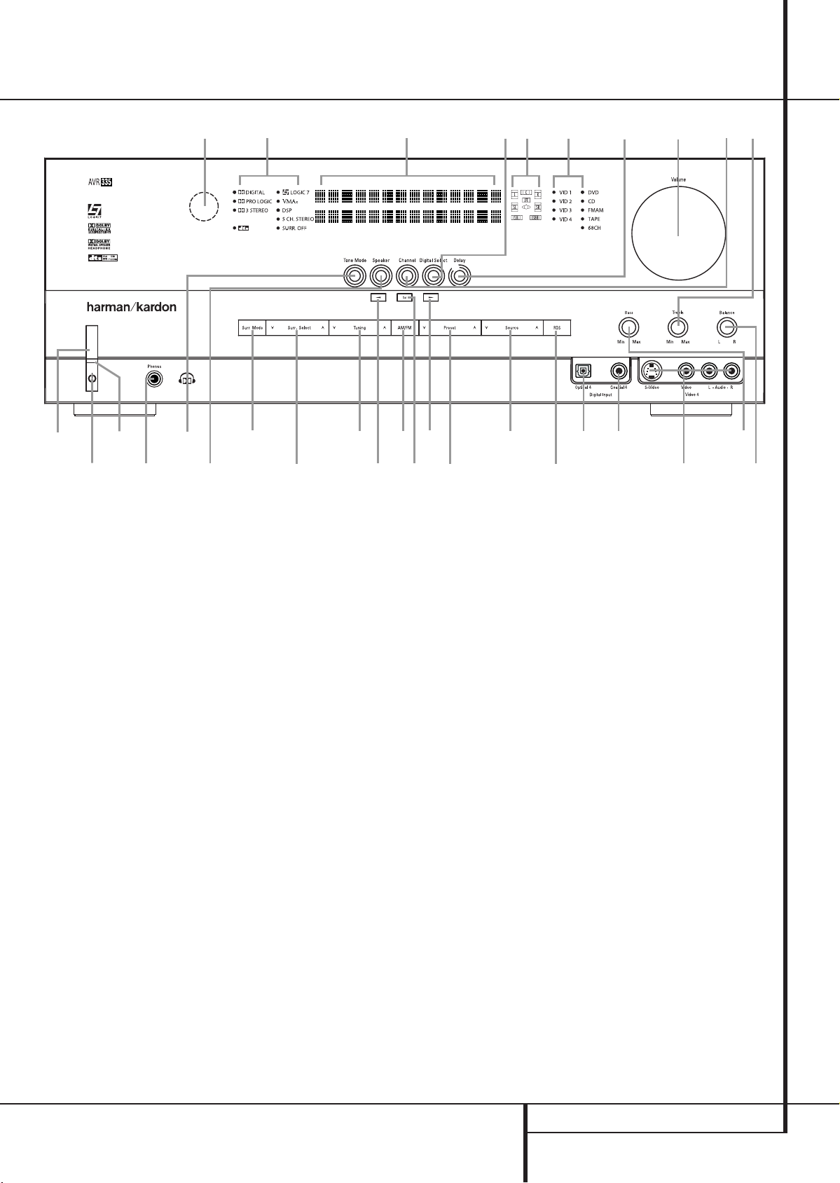
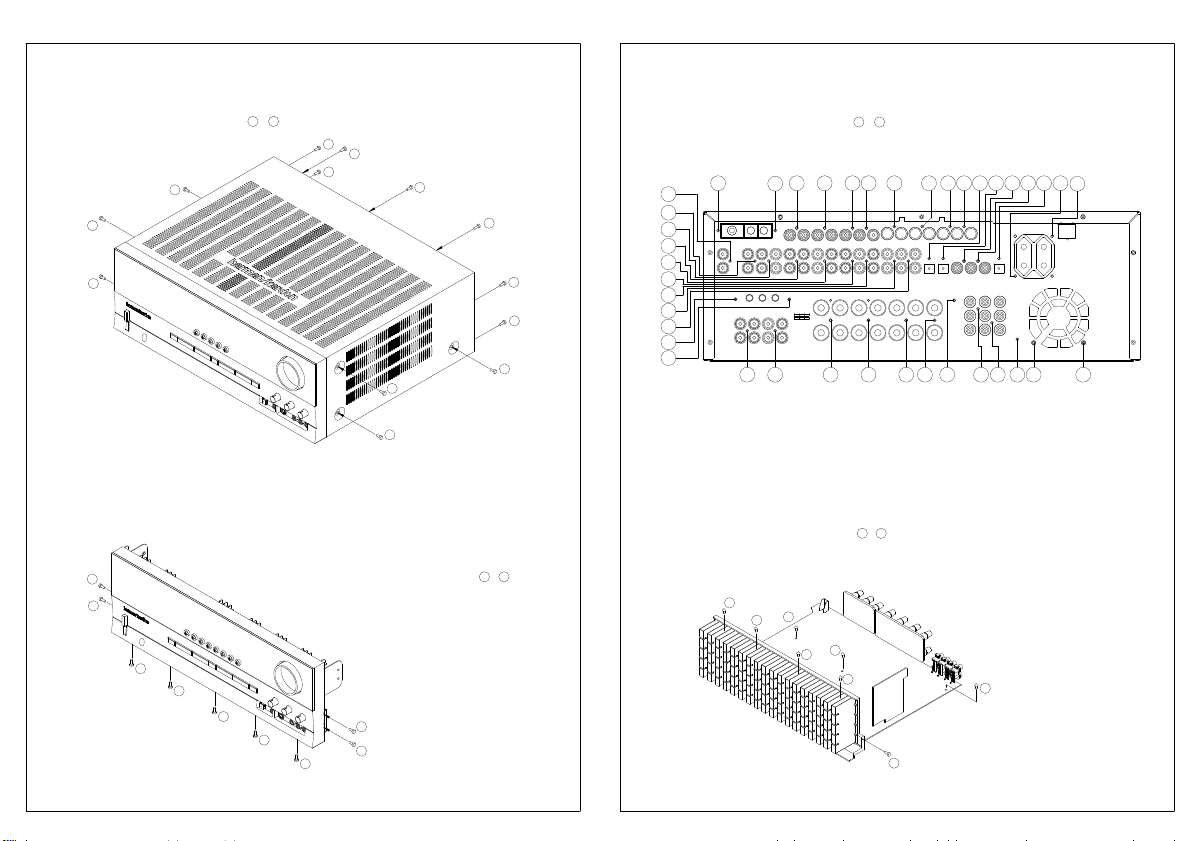
Rear Panel Connections
AM Antenna
FM Antenna
Tape Inputs
Tape Outputs
Subwoofer Output
DVD Audio Inputs
CD Inputs
Multiroom Outputs
Fan Vents
8-Channel Direct Inputs
Digital Audio Outputs
Video Monitor Outputs
DVD Video Inputs
NOTE: To assist in making the correct connections for multichannel input/output and speaker
connections, all connection jacks and terminals
have been color coded in conformance with the
latest CEA standards as follows:
Front Left: White
Front Right: Red
Center: Green
Surround Left: Blue
Surround Right: Gray
Surround Back Left: Brown
Surround Back Right: Tan
Subwoofer (LFE): Purple
Digital Audio: Orange
Composite Video: Yellow
Component Video “Y”: Green
Component Video “Pr”: Red
Component Video “Pb”: Blue
AM Antenna: Connect the AM loop antenna
supplied with the receiver to these terminals. If an
external AM antenna is used, make connections to
the AM and GND terminals in accordance with
the instructions supplied with the antenna.
Front Speaker Outputs
Center Speaker Outputs
Surround Speaker Outputs
Switched AC Accessory Outlet
Unswitched AC Accessory Outlet
AC Power Cord
Video 2 Component Video Inputs
Component Video Outputs
DVD Component Video Inputs
Remote IR Output
Remote IR Input
Multiroom IR Input
Video 1 Video Outputs
FM Antenna: Connect the supplied indoor or
an optional external FM antenna to this terminal.
Tape Inputs: Connect these jacks to the
PLAY/OUT jacks of an audio recorder.
Tape Outputs: Connect these jacks to the
RECORD/INPUT jacks of an audio recorder.
Subwoofer Output: Connect this jack to
the line-level input of a powered subwoofer. If an
external subwoofer amplifier is used, connect this
jack to the subwoofer amplifier input.
DVD Audio Inputs: Connect these jacks to
the analog audio jacks on a DVD or other audio
or video source.
CD Inputs: Connect these jacks to the
analog output of a compact disc player or CD
changer or any other audio source.
Multiroom Outputs: Connect these jacks
to an optional audio power amplifier to listen to
the source selected by the multiroom system in a
remote room.
Video 1 Video Inputs
Video 2 Video Outputs
Video 3 Video Inputs
Video 2 Video Inputs
Optical Digital Inputs
Coaxial Digital Inputs
Video 2 Audio Outputs
Video 2 Audio Inputs
Video 3 Audio Inputs
Video 1 Audio Inputs
Video 1 Audio Outputs
Preamp Outputs
Surround Back/Multiroom Speaker Outputs
Fan Vents: These ventilation holes are the
output of the AVR 335’s airflow system. To
ensure proper operation of the unit and to avoid
possible damage to delicate surfaces, make
certain that these holes are not blocked and that
there is at least three inches of open space
between the vent holes and any wooden or
fabric surface.
8-Channel Direct Inputs: These jacks are
used for connection to source devices such as
DVD-Audio or SACD players with discrete analog
outputs. Depending on the source device in use,
all eight jacks may be used, though in many
cases only connections to the front left/right,
center, surround left/right and LFE (subwoofer
input) jacks will be used for standard 5.1 audio
signals.
Digital Audio Outputs: Connect these
jacks to the matching digital input connector on
a digital recorder such as a CD-R or MiniDisc
recorder.
REAR PANEL CONNECTIONS
Page 6

Rear Panel Connections
Video Monitor Outputs: Connect this jack
to the composite and/or S-Video input of a TV
monitor or video projector to view the on-screen
menus and the output of any standard Video or
S-Video source selected by the receiver’s video
switcher.
DVD Video Inputs: Connect these jacks to
the composite or S-Video output jacks on a DVD
player or other video source.
Front Speaker Outputs: Connect these
outputs to the matching + or – terminals on
your left and right speakers. In conformance with
the new CEA color code specification, the White
terminal is the positive, or "+" terminal that
should be connected to the red (+) terminal on
Front Left speaker with the older color coding,
while the Red terminal is the positive, or "+"
terminal that should be connected to the red (+)
terminal on Front Right speaker. Connect the
black (–) terminals on the AVR to the black (–)
terminals on the speakers. See page 13 for more
information on speaker polarity.
Center Speaker Outputs: Connect these
outputs to the matching + and – terminals on
your center channel speaker. In conformance
with the new CEA color code specification, the
Green Terminal is the positive, or "+" terminal
that should be connected to the red (+) terminal
on speakers with the older color coding. Connect
the black (–) terminal on the AVR to the black
negative (–) terminal on your speaker. (See page
13 for more information on speaker polarity.)
Surround Speaker Outputs: Connect
these outputs to the matching + and – terminals
on your surround channel speakers. In conformance with the new CEA color code specification, the Blue terminal is the positive, or "+"
terminal that should be connected to the red (+)
terminal on the Surround Left speaker with older
color coding, while the Gray terminal should be
connected to the red (+) terminal on the
Surround Right speaker with the older color
coding. Connect the black (–) terminal on the
AVR to the matching black negative (–)
terminals for each surround speaker. (See page
13 for more information on speaker polarity.)
Switched AC Accessory Outlet: This
outlet may be used to power any device that you
wish to have turn on when the AVR is turned on
with the System Power Control switch
Unswitched AC Accessory Outlet: This
outlet may be used to power any AC device. The
power will remain on at this outlet regardless of
whether the AVR is on or off (in Standby), provided that the Main Power switch
1
2
is on.
.
Note: The total power consumption of all
devices connected to the accessory outlets
should not exceed 100 watts from the
Unswitched Outlet
Switched Outlet
AC Power Cord: Connect the AC plug to an
unswitched AC wall output.
Video 2 Component Video Inputs:
Connect the Y/Pr/Pb component video outputs of
an HDTV Set-top convertor, satellite receiver, or
other video source device with component video
outputs to these jacks.
Monitor Component Video Outputs:
Connect these outputs to the component video
inputs of a video projector or monitor. When a
source connected to one of the two
Component Video Inputs
the signal will be sent to these jacks.
DVD Component Video Inputs: Connect
the Y/Pr/Pb component video outputs of a DVD
player to these jacks.
Note: All component inputs/outputs can be
used for RGB signals too, in the same way as
described for the Y/Pr/Pb signals, then connected
to the jacks with the corresponding color.
RGB connection is not possible if the source outputs a separate sync signal (see page 14).
Remote IR Output: This connection permits
the IR sensor in the receiver to serve other
remote controlled devices. Connect this jack to
the “IR IN” jack on Harman Kardon or other
compatible equipment.
Remote IR Input: If the AVR’s front-panel
IR sensor is blocked due to cabinet doors or
other obstructions, an external IR sensor may
be used. Connect the output of the sensor to
this jack.
Multiroom IR Input: Connect the output of
an IR sensor in a remote room to this jack to
operate the AVR’s multiroom control system.
Video 1 Video Outputs: Connect these
jacks to the RECORD/INPUT composite or
S-Video jack on a VCR.
Video 1 Video Inputs: Connect these jacks
to the PLAY/OUT composite or S-Video jacks on
a VCR or other video source.
Video 2 Video Outputs: Connect these
jacks to the RECORD/INPUT composite or
S-Video jacks on a second VCR.
Video 3 Video Inputs: Connect these jacks
to the PLAY/OUT composite or S-Video jacks on
any video source.
Video 2 Video Inputs: Connect these jacks
to the PLAY/OUT composite or S-Video jacks on
a second VCR or other video source.
and 50 W from the
.
is selected
Optical Digital Inputs: Connect the
optical digital output from a DVD player, HDTV
receiver, the output of a compatible computer
sound card playing MP3 files or streams, LD
player, MD player or CD player to these jacks.
The signal may be either a Dolby Digital signal, a
DTS signal, a 2 channel MPEG 1 signal, or a
standard PCM digital source.
Coaxial Digital Inputs: Connect the coax
digital output from a DVD player, HDTV receiver,
the output of a compatible computer sound card
playing MP3 files or streams, LD player, MD
player or CD player to these jacks.The signal
may be either a Dolby Digital signal, DTS signal,
a 2 channel MPEG 1 signal, or a standard PCM
digital source. Do not connect the RF digital output of an LD player to these jacks.
Video 2 Audio Outputs: Connect these
jacks to the RECORD/INPUT audio jacks on a
VCR or any Audio recorder.
Video 2 Audio Inputs: Connect these jacks
to the PLAY/OUT audio jacks on a second VCR
or other audio or video source.
Video 3 Audio Inputs: Connect these jacks
to the PLAY/OUT audio jacks on any audio or
video source.
Video 1 Audio Inputs: Connect these jacks
to the PLAY/OUT audio jacks on a VCR or other
audio or video source.
Video 1 Audio Outputs: Connect these
jacks to the RECORD/INPUT audio jacks on
a VCR or any other Audio recorder.
Preamp Outputs: Connect these jacks to
an optional, external power amplifier for applications where higher power is desired.
Surround Back/Multiroom Speaker
Outputs: These speaker terminals are normally
used to power the surround back left/surround
back right speakers in a 7.1 channel system.
However, they may also be used to power the
speakers in a second zone, which will receive the
output selected for a multiroom system.
To change the output fed to these terminals
from the default of the Surround Back speakers
to the Multiroom Output, you must change a
setting in the
OSD system. See page 39 for more information
on configuring this speaker output. In normal
surround system use, the brown and black terminals are the surround back left channel positive
(+) and negative (–) connections and the tan
and black terminals are the surround back right
positive (+) and negative (–) terminals.
For multiroom use, connect the brown and black
SBL terminals to the red and black connections
on the left remote zone speaker and connect the
tan and black SBR terminals to the red and black
terminals on the right remote zone speaker.
MULTIROOM MENU of the
REAR PANEL CONNECTIONS
Page 7
35
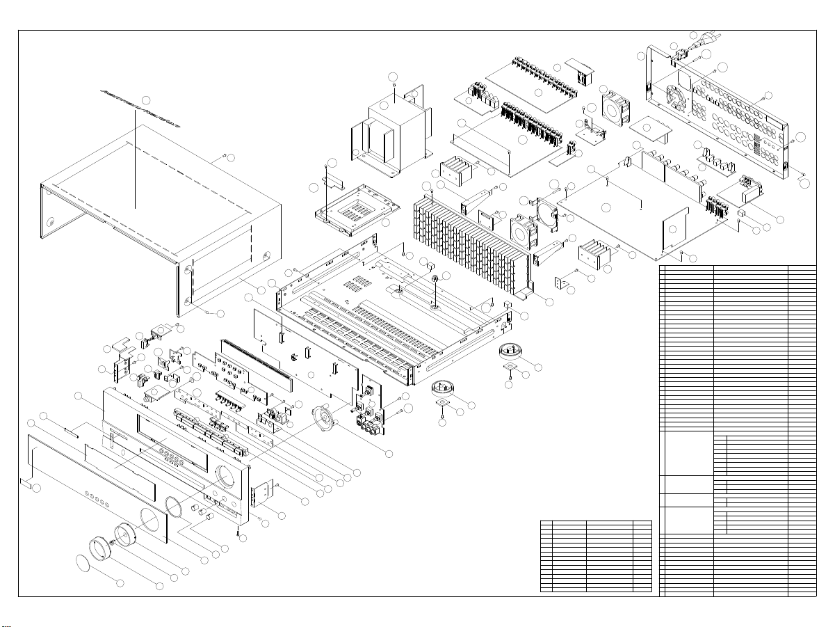
AVR335/230 EXPLODED VIEW
S9
45
40-4
36
40-3
S11
S1
37-9
S5
22
21
20
S7
S2
37-5
15
51
S2
50
13
8
7
6
S2
53
14
S2
S3
16
37-4
54
37-2
37-1
S2
37-8
40-5
S4
18
30
S12
29
S5
50
S5
S5
S4
28
S10
S4
S2
37-3
S14
24
23
S4
19
17
48
12
46
9
S1
S1
5
31
4
3
18
2
1
47
11
10
S2
38-2
40-1
42
S10
44
39-1
39-2
S6
S15
S4
43
38-1
S5
S5
18
S5
27
26
25
24
23
DESCRIPTION
SCREW
SCREW
SCREW
SCREW
SCREW
SCREW
SCREW
SCREW
SCREW,TRANS
SCREW
SCREW,SPECIAL
SCREW,SPECIAL
SCREW
SCREW,SPECIAL
PARTS NO.
CTB3+8JFC
CTB3+10G
CTWS3+10G
CTW3+8J
CTB3+8J
CTW3+12J
CTB4+6FFC
CTB3+10GFZ
CHD1A023
CTB3+6J
CHD1A012Z
CHD4A012
CTB3+8JFZ
CHD1A036FZ 4
NO
S1
S2
S3
S4
S5
S6
S7
S8
S9
S10
S11
S12
S13
S14
S15
34
33
S15
40-2
32
32
3
8
-3
37-7
S5
Q,ty
17
37
1
9
15
3
6
34
4
19
2
5
3
2CTB3+16GFZSCREW
S4
DESCRIPTION
NO
CAP,VOLUME
1
HOLDER,VOLUME
2
INDICATOR,VOLUME
3
WINDOW,FIP
4
5
KNOB,ROTARY
FILTER,FIP
6
BDAGE,HARMAN/KARDON
7
PANEL,FRONT
8
BRACKET,SIDE
9
KNOB,FUNCTION
10
KNOB,SET
11
KNOB,DELAY
12
KNOB,POWER
13
INDICATOR,POWER
14
KNOB,MOMS
15
BRACKET,PCB CMK1A010
16
PLATE,SHIELD
17
HEAT SINK CMY1A249 2
18
HOLDER,LED
19
BRACKET,FIP
20
CABINET,TOP
21
CHASSIS,BOTTOM
22
RUBBER,CUSHION
23
FOOT
24
SUPPORT,CUSHION
25
HEAT SINK
26
BRACKET,PCB
27
HOLDER,PCB
28
BRACKET,TRANS
29
BRACKET,PCB(H/T)
30
31
BRACKET,PCB
32
PANEL,REAR
33
BUSHING,AC CORD
34
CORD,POWER
35
TRANS,POWER
36
FRONT PAB ASS'Y
37
MAIN PCB ASS'Y COP11746D 1
38
INPUT PCB ASS'Y COP11749D 1
39
VIDEO PCB ASS'Y40COP11747D 1
TUNER MODULE
41
FAN
42
BRACKET,FAN
43
BRACKET,FAN CMD1A506
44
BADGE,TOP
45
BADGE,MODEL
46
INSULATOR,FUNCTION
47
INSULATOR,SET
48
CUSHION,RUBBER
49
CUSHION
50
BRACKET,SIDE(L) CMD1A555 1
51
RUBBER CHG1A309 1
52
INSULATOR,POWER CMX1A170 2
53
INSULATOR,FUNCTION(L) CMX1A173 2
54
S13
S8
41
49
S4
PARTS NO.
CGX1A338MBC22
CMH1A214
CGL1A222
CGU1A317X
CBN1A174MBC22
CMZ1A088
KGB1A111X
CGW1A366RDWH43
CMD2A443
CBT1A905MBYC22
CBT1A904MBZC22
CBT1A819K128
CBT1A903MMZC22
CGL1A221
CBC1A147MBZC22
CMC1A200
CMH1A215
CMD1A209
CKC4B145S46
CUA1A229
KHG1A050
CKL2A069H43
CHG1A104
CMY2A205
CMD1A417
CHE1A170
CMD1A487
CMD1A398
CMD1A398SHEET,VOLUME 1
CMD1A387
CKF2A294Z
KHR1A028
CJA2B043ZA
CLT5W018ZE
COP11745D
FIP PCB
37-1
KEY PCB
37-2
TONE PCB
37-3
PHONE PCB
37-4
MOMS PCB
37-5
POWER LED PCB
37-6
CONNECTOR PCB
37-7
DIGITAL INPUT PCB
37-8
DOWNLOAD PCB 1
37-9
MAIN PCB
38-1
AC OUTLETS PCB
38-2
REMOTE PCB
38-3
INPUT PCB
39-1
MULTI OUT PCB 1
39-2
VIDEO PCB 1
40-1
COMPONEANT VIDEO PCB
40-2
DIGITAL INPUT/OUTPUT PCB
40-3
TRANS PCB
40-4
TRANS PCB
40-5
CNVM9014MS170L
HDMKD1206PTS3 2
CMD1A488
CGB1A152Z
KGB1A148Z 1
CMX1A148
CMX1A149
CHG1A157
CHG1A160
S13
S10
Q,ty
1
1
1
1
3
1
1
1
1
1
1
1
1
1
1
1
1
1
3
1
1
4
4
2
1
2
2
1
2
4
1
1
1
1
1
1
1
1
1
1
1
1
1
1
1
1
1
1
1
1
1
1
1
1
1
1
2
1
1
1
Page 8
DISASSEMBLY
AVR335/230
1. Removing the Top Cabinet
Remove the Screws
6
4
5
9
8
7
6
13
1
~
10
9
11
7
8
12
13
3
1
2
Remove the Screws
10
11
12
13
14
15
16
17
18
19
27
28
8
9
3029
41
1
~
57 6 4 3 2 1 20 21
3231 33 34 35 36 37
22
38
39 40
2523 24
26
4. Removing the Main PCB
3. Removing the Rear Panel
1 8
Remove the Screws
~
2. Removing the Front Panel
Remove the Screws
5
4
1
2
3
1 9
~
1
5
2
6
3
4
8
7
Page 9
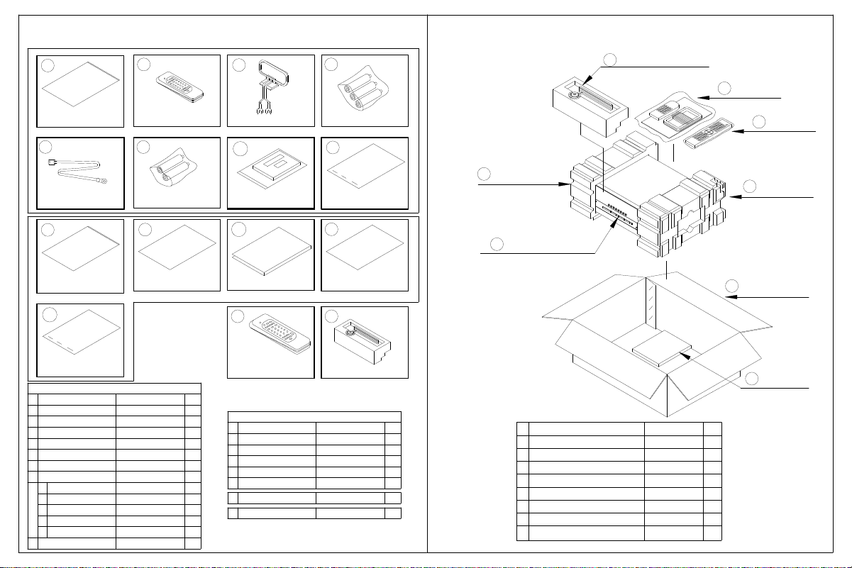
1. Instruction manual ass'y - Accessories 2. Package Drawing
1
POLY BAG
2
REMOCON
TRANSMITTER ASS'Y
3
AM LOOP ANTENNA ASS'Y
4
BATTERY ASS'Y
MICROPHONE ASS'Y
8
AVR335/230
ACCESSORY-1
1
REMOCON ASS'Y
2
5
FM 1 POLE ANT
9
POLY BAG
6
BATTERY ASS'Y
10
BOOKLET,INFORMATION
13
STAPLE
ACCESSORY-1
NO DESCRIPTION PARTS NO. Q,ty
1
2
REMOCON ASS'Y
3
4
5
FM 1 POL ANT(UL) CSA1A018Z 1
6 HABAAAM1.5VBATTERY 2
7
COVER ASS'Y CGRAVR130/230ZA
1
COVER A
2
COVER B
3
SHEET,FRONT COVER
4
PAD , COVER
5
BAG , POLY
8
STAPLE KPL0905 3
CPB1061YPOLY BAG
HARTZONE2
CSA1A027ZAM LOOP ANTENNA ASS'Y 1
HABAAAM1.5VHKBATTERY 3
CGR1A331M7H43 1
CQE1A220Z
CPS1A676 1
CPB1A176Z 1
7
COVER ASS'Y
11
MANUAL INSTRUCTION
A
REMOCON ASS'Y
1
1
1
1
1CGR1A332M7H43
1
ACCESSORY-2
NO DESCRIPTION PARTS NO. Q,ty
9
BOOKLET,INFORMATION
10
11
12
MANUAL ,SETUP GUIDE
13
STAPLE KPL0905 3
A REMOCON ASS'Y HARTAVR335/230 1
B MICROPHONE ASS'T AVR335MICRO 1
8
STAPLE
12
MANUAL SETUP GUIDE
B
MICROPHONE ASS'Y
CQE1A180Z 1
CQX1A954ZMANUAL,INSTRUCTION
CQX1A1014Z
3
SNOW PAD (L)
SET
5
1CPB1061YPOLY BAG
1
1
DESCRIPTIONNO
ACCESSORY-1
1
2
3
SNOW,PAD(L)
4
SNOW,PAD(R)
5
SET
BOX,OUT CARTON
6
ACCESSORY-2 CQXAVR335/230
7
CQXAVR335/230
HARTAVR335/230
CPS4A564
CPS4A565
AVR335/230SET
CPG1A775U
Q,tyPARTS NO.
1
1REMOCON ASS'Y
1
1
1
1
1
1MICROPHONE ASS'Y AVR335MICRO8
SNOW PAD (R)
4
BOX ,OUT CARTON
6
ACCESSORY-2
7
Page 10

FRONT PCB
Ref# Description Drawing No Component Qty
FRONT PCB ASS'Y COP11745G 1
BAT1 BATTERY , RECHARGEABLE GP15BNH3A3H HGP15BNH3A3H 1
BK71 BRACKET , FLT A4-92-1739 CMD1A209 1
BK72 BRACKET , FLT A4-92-1739 CMD1A209 1
BK73 BRACKET , PCB CMD1A387 1
BK74 BRACKET , FLT A4-92-1739 CMD1A209 1
BN10 WIRE ASS'Y (SHIELD) CWZAVR230BN10 1
BN15 WIRE ASS'Y CWB2B906150EN 1
BN16 WIRE ASS'Y (SHIELD) CWZAVR2550BN16 1
BN18 WIRE ASS'Y (SHIELD) CWZAVR125BN18 1
BN41 WIRE ASS'Y (SHIELD) CWZAVR130BN41 1
BN72 CONN,FFC 1M/M 32P STR,SMD_JST 32FMNNBMTTNATF HJP32GA179ZJ 1
BN80 WIRE ASS'Y CWB2B911420EW 1
BN81 WIRE , ASS'Y CWB2B908250BM 1
BN84 WIRE ASS'Y CWB2B905080EN 1
BN85 WIRE ASS'Y CWB2B902090EN 1
BN87 WIRE ASS'Y (SHIELD) CWZAVR2550BN87 1
BN88 WIRE ASS'Y CWB2B904070EN 1
BN89 WIRE ASS'Y CWB2B905080EN 1
BN90 WIRE ASS'Y CWB2B902090EN 1
BN94 CONNECTOR MOLEX35237-1310 KJP13GB99ZM 1
BN95 CONNECTOR , HOUSING MOLEX35237-0810 KJP08GB99ZM 1
C701 CAP , CERAMIC 39PF 50V J HCBS1H390JT 1
C702 CAP , CERAMIC 39PF 50V J HCBS1H390JT 1
C703 CAP , CERAMIC 820PF 50V K HCBS1H821KBT 1
C704 CAP , ELECT 10UF 35V HCEA1VH100T 1
C705 CAP , CERAMIC 1000PF 50V B HCBS1H102KBT 1
C706 CAP , CERAMIC 560PF 50V HCBS1H561KBT 1
C708 CAP , CERAMIC 0.022UF 50V Z HCBS1H223ZFT 1
C709 CAP , ELECT 100UF 16V CCEA1CH101T 1
C710 CAP , ELECT 2.2UF 50V CCEA1HH2R2T 1
C711 CAP , CERAMIC 1000PF 50V B HCBS1H102KBT 1
C712 CAP , ELECT 1UF 50V HCEA1HH1R0T 1
C713 CAP , CERAMIC 0.022UF 50V Z HCBS1H223ZFT 1
C714 CAP , CERAMIC 150PF 50V K HCBS1H151KBT 1
C715 CAP , ELECT 4.7UF 50V HCEA1HH4R7T 1
C716 CAP , ELECT 330UF 16V HCEA1CH331T 1
C719 CAP , CERAMIC 180PF 50V K HCBS1H181KBT 1
C720 CAP , CERAMIC 180PF 50V K HCBS1H181KBT 1
C721 CAP , CERAMIC 180PF 50V K HCBS1H181KBT 1
C723 CAP , CERAMIC 0.1UF 50V Z HCBS1H104ZFT 1
C724 CAP , CERAMIC 0.022UF 50V Z HCBS1H223ZFT 1
C725 CAP , CERAMIC 0.047UF 50V ZF CCKT1H473ZF 1
C726 CAP , ELECT 100UF 16V HCEA1CH101T 1
C728 CAP , CERAMIC 0.1UF 50V Z HCBS1H104ZFT 1
C729 CAP , CERAMIC 0.047UF 50V ZF CCKT1H473ZF 1
C730 CAP , CERAMIC 0.1UF 50V Z HCBS1H104ZFT 1
C731 CAP , ELECT 10UF 50V HCEA1HH100T 1
C735 CAP , ELECT 100UF 16V CCEA1CH101T 1
C736 CAP , CERAMIC 0.022UF 50V Z HCBS1H223ZFT 1
C737 CAP , CERAMIC 12PF 50V J HCBS1H120JCT 1
C738 CAP , CERAMIC 12PF 50V J HCBS1H120JCT 1
C739 CAP , ELECT 220UF/10V CCEA1AH221T 1
C740 CAP , ELECT 10UF 35V CCEA1VH100T 1
C770 CAP , CERAMIC 0.022UF 50V Z HCBS1H223ZFT 1
C771 CAP , CERAMIC 0.022UF 50V Z HCBS1H223ZFT 1
C773 CAP , ELECT 10UF 35V HCEA1VH100T 1
C774 CAP , ELECT 10UF 35V HCEA1VH100T 1
Harman Consumer group International Bill of material AVR335/230
Page 11

FRONT PCB
Ref# Description Drawing No Component Qty
C775 CAP , CERAMIC 150PF 50V K HCBS1H151KBT 1
C776 CAP , CERAMIC 150PF 50V K HCBS1H151KBT 1
C777 CAP , ELECT 10UF 35V HCEA1VH100T 1
C778 CAP , ELECT 10UF 35V HCEA1VH100T 1
C779 CAP , ELECT 47UF 16V HCEA1CKS470T 1
C780 CAP , ELECT 47UF 16V HCEA1CKS470T 1
C781 CAP , ELECT 10UF 16V HCEA1CKS100T 1
C782 CAP , ELECT 10UF 16V HCEA1CKS100T 1
C785 CAP , CERAMIC 47PF 50V J HCBS1H470JT 1
C786 CAP , CERAMIC 47PF 50V J HCBS1H470JT 1
C787 CAP , ELECT 10UF 16V HCEA1CKS100T 1
C788 CAP , ELECT 10UF 16V HCEA1CKS100T 1
C789 CAP , ELECT 10UF 16V HCEA1CKS100T 1
C790 CAP , ELECT 10UF 16V HCEA1CKS100T 1
C791 CAP , ELECT 47UF 16V HCEA1CKS470T 1
C792 CAP , ELECT 47UF 16V HCEA1CKS470T 1
C793 CAP , FILM 0.018UF 63V J KCFE1J183JBT 1
C794 CAP , FILM 0.018UF 63V J KCFE1J183JBT 1
C795 CAP , FILM 0.082UF 63V J KCFE1J823JBT 1
C796 CAP , FILM 0.082UF 63V J KCFE1J823JBT 1
C797 CAP , FILM 0.0033UF 63V J KCFE1J332JBT 1
C798 CAP , FILM 0.0033UF 63V J KCFE1J332JBT 1
C799 CAP , FILM 0.018UF 63V J KCFE1J183JBT 1
C800 CAP , FILM 0.018UF 63V J KCFE1J183JBT 1
C805 CAP , CERAMIC 0.022UF 50V Z HCBS1H223ZFT 1
C806 CAP , CERAMIC 0.022UF 50V Z HCBS1H223ZFT 1
C807 CAP , SEMICONDUCTOR 0.1UF 50V ZF CCFT1H104ZF 1
C808 CAP , CERAMIC 180PF 50V KB CCKT1H181KB 1
C809 CAP , ELECT 470UF 10V HCEA1AH471T 1
C810 CAP , ELECT 100UF 16V HCEA1CH101T 1
C811 CAP , ELECT 100UF 16V HCEA1CH101T 1
C812 CAP , SEMICONDUCTOR 0.1UF 50V ZF CCFT1H104ZF 1
C813 CAP , ELECT 4.7UF 50V HCEA1HH4R7T 1
C814 CAP , ELECT 4.7UF 50V HCEA1HH4R7T 1
C815 CAP , CERAMIC 0.022UF 50V Z HCBS1H223ZFT 1
C816 CAP , CERAMIC 0.022UF 50V Z HCBS1H223ZFT 1
C817 CAP , CERAMIC 10PF 50V DC CCCT1H100DC 1
C853 CAP , CERAMIC(KH TYPE) DKS471ME KCKDKS471ME 1
C855 CAP , CERAMIC 100PF 50V K HCBS1H101KBT 1
C856 CAP , CERAMIC 100PF 50V K HCBS1H101KBT 1
C857 CAP , CERAMIC 0.1UF 50V Z HCBS1H104ZFT 1
C859 CAP , CERAMIC 0.022UF 50V Z HCBS1H223ZFT 1
C860 CAP , CERAMIC 0.022UF 50V Z HCBS1H223ZFT 1
C861 CAP , CERAMIC 0.022UF 50V Z HCBS1H223ZFT 1
C862 CAP , CERAMIC 100PF 50V K HCBS1H101KBT 1
C863 CAP , CERAMIC 100PF 50V K HCBS1H101KBT 1
C864 CAP , ELECT 1000UF 6.3V CCEA0JH102T 1
C865 CAP , ELECT 1000UF 6.3V CCEA0JH102T 1
C874 CAP , CERAMIC 100PF 50V K HCBS1H101KBT 1
C875 CAP , CERAMIC 100PF 50V K HCBS1H101KBT 1
C876 CAP , CERAMIC 100PF 50V K HCBS1H101KBT 1
C877 CAP , CERAMIC 0.047UF 50V Z HCBS1H473ZFT 1
C878 CAP , CERAMIC 0.047UF 50V Z HCBS1H473ZFT 1
C882 CAP , CERAMIC 0.1UF 50V Z HCBS1H104ZFT 1
C886 CAP , ELECT 1000UF 6.3V CCEA0JH102T 1
C889 CAP , CERAMIC 22PF 50V J HCBS1H220JCT 1
C890 CAP , CERAMIC 22PF 50V J HCBS1H220JCT 1
C891 CAP , CERAMIC 0.022UF 50V Z HCBS1H223ZFT 1
Harman Consumer group International Bill of material AVR335/230
Page 12

FRONT PCB
Ref# Description Drawing No Component Qty
C892 CAP , CERAMIC 0.022UF 50V Z HCBS1H223ZFT 1
C893 CAP , CERAMIC 0.022UF 50V Z HCBS1H223ZFT 1
C894 CAP , CERAMIC 0.022UF 50V Z HCBS1H223ZFT 1
C895 CAP , ELECT 470UF 10V HCEA1AH471T 1
C896 CAP , CERAMIC 0.022UF 50V Z HCBS1H223ZFT 1
C897 CAP , ELECT 470UF 10V HCEA1AH471T 1
C900 CAP , CERAMIC 0.1UF 50V Z HCBS1H104ZFT 1
C901 CAP , CERAMIC 0.1UF 50V Z HCBS1H104ZFT 1
C903 CAP , ELECT 2.2UF 50V HCEA1HH2R2T 1
C905 CAP , ELECT 2.2UF 50V HCEA1HH2R2T 1
CB72 CABLE , CARD CWC1B2A32A250B 1
CN10 WAFER MOLEX 53015 KJP04GB46ZM 1
CN11 WAFER MOLEX35336-1510 KJP15GA98ZM 1
CN12 WAFER MOLEX35336-1510 KJP15GA98ZM 1
CN16 WAFER KJP08GB46ZM 1
CN79 WAFER MOLEX53014-0510 KJP05GA19ZM 1
CN84 WAFER MOLEX53014-0510 KJP05GA19ZM 1
CN86 WAFER MOLEX35328-02 KJP02GA89ZM 1
CN88 WAFER KJP04GA19ZM 1
CN89 WAFER MOLEX53014-0510 KJP05GA19ZM 1
CN90 WAFER KJP02GA19ZM 1
D701 BLUE L.E.D CVD52CSBBCEAB2 1
D703 BLUE L.E.D CVD52CSBBCEAB2 1
D705 BLUE L.E.D CVD52CSBBCEAB2 1
D723 L.E.D , 2 COLOR (ORG , BLUE) TOL-50BOBBWGA CVD50BOBBWGA 1
D724 DIODE 1SS133T-77 HVD1SS133MT 1
D725 DIODE 1SS133T-77 HVD1SS133MT 1
D726 DIODE 1SS133T-77 HVD1SS133MT 1
D727 DIODE 1SS133T-77 HVD1SS133MT 1
D728 DIODE 1SS133T-77 HVD1SS133MT 1
D729 DIODE 1SS133T-77 HVD1SS133MT 1
D730 DIODE 1SS133T-77 HVD1SS133MT 1
D774 DIODE 1SS133T-77 HVD1SS133MT 1
D778 DIODE 1N4003 KVD1N4003ST 1
D779 DIODE 1SS133T-77 HVD1SS133MT 1
D780 DIODE 1SS133T-77 HVD1SS133MT 1
D781 DIODE 1SS133T-77 HVD1SS133MT 1
D782 DIODE 1N4003 KVD1N4003ST 1
D783 DIODE 1SS133T-77 HVD1SS133MT 1
D786 DIODE , ZENER 5,6 HVDMTZJ5.6BT 1
D787 DIODE , ZENER 5,6 HVDMTZJ5.6BT 1
D788 DIODE , ZENER 5,6 HVDMTZJ5.6BT 1
D789 DIODE , ZENER 5,6 HVDMTZJ5.6BT 1
FIP1 F.I.P HFLHCA18ML01 1
IC71 I.C , RDS FILTER TW SAA6579T/V1 BVISAA6579TV1 1
IC72 IC , FLASH U-COM FUJITSU BVIMB90F482APFG 1
IC73 SENSOR , REMOTE RPM6938-H4 HRVRPM6938H4 1
IC74 I.C , U-COM HVIANAM1385AT 1
IC75 I.C , HEX HVI74ACT04MTR 1
IC76 IC , INVERTER TC74HCU04AFN HVITC74HCU04AFN 1
IC80 I.C HVIHCF4053M013T 1
IC81 I.C , OP AMP NJM2068MD-TE1 HVINJM2068MDTE1 1
IC82 I.C , OP AMP NJM2068MD-TE1 HVINJM2068MDTE1 1
IC83 I.C , HEX HVI74ACT04MTR 1
IC84 I.C , HEX HVI74ACT04MTR 1
IC85 I.C , RESET RICOH 1.8V HVIRH5VT18C 1
IC87 IC , RESET HVIRE5VL28CATZ 1
IC88 I.C , OP AMP NJM2068MD-TE1 HVINJM2068MDTE1 1
Harman Consumer group International Bill of material AVR335/230
Page 13

FRONT PCB
Ref# Description Drawing No Component Qty
IC89 I.C HVIHCF4053M013T 1
JK81 JACK , BOARD (COAX) CJJ4M041Y 1
JK82 MODULE , OPTICAL(RX) TORX179L HJSTORX179L 1
JK85 JACK , S-VIDEO CJJ9M003Z 1
JK86 JACK , BOARD CJJ4S023Y 1
JW81 WIRE ASS'Y CWE7202110AA 1
JW83 WIRE ASS'Y CWE8202150RV 1
JW84 WIRE, ASS'Y CWE8202110RV 1
JW85 WIRE ASS'Y CWE8202070AA 1
L702 COIL , AXAIL HLQ02C100KT 1
Q701 T.R KRC107M HVTKRC107MT 1
Q702 T.R KRC107M HVTKRC107MT 1
Q703 T.R KRC107M HVTKRC107MT 1
Q704 T.R KRC107M HVTKRC107MT 1
Q705 T.R KRC107M HVTKRC107MT 1
Q706 T.R KRC107M HVTKRC107MT 1
Q722 T.R KRA107M HVTKRA107MT 1
Q723 T.R KRC107M HVTKRC107MT 1
Q724 T.R KRC107M HVTKRC107MT 1
Q725 T.R KRC107M HVTKRC107MT 1
Q726 T.R KRC107M HVTKRC107MT 1
Q727 T.R KRC107M HVTKRC107MT 1
Q728 T.R KRC107M HVTKRC107MT 1
Q729 T.R KRC107M HVTKRC107MT 1
Q731 T.R KSA1175Y KVTKSA1175YT 1
Q732 T.R KRC107M HVTKRC107MT 1
Q733 T.R KSC2785Y KVTKSC2785YT 1
Q736 T.R , MUTE KTC2874B HVTKTC2874BT 1
Q738 T.R KRC107M HVTKRC107MT 1
Q739 T.R KTA1271Y HVTKTA1271YT 1
Q740 T.R KRC107M HVTKRC107MT 1
Q741 T.R KRC107M HVTKRC107MT 1
Q743 T.R KRA107M HVTKRA107MT 1
R701 RES , CARBON 10K OHM 1/5W J CRD20TJ103T 1
R702 RES , CARBON 1 OHM 1/5W J CRD20TJ1R0T 1
R703 RES , CARBON 10K OHM 1/5W J CRD20TJ103T 1
R704 RES , CARBON 10 OHM 1/5W J CRD20TJ100T 1
R705 RES , CARBON 82 OHM 1/5W J CRD20TJ820T 1
R706 RES , CARBON 82 OHM 1/5W J CRD20TJ820T 1
R707 RES , CARBON 82 OHM 1/5W J CRD20TJ820T 1
R708 RES , CARBON 82 OHM 1/5W J CRD20TJ820T 1
R709 RES , CARBON 47 OHM 1/5W J CRD20TJ470T 1
R710 RES , CARBON 47 OHM 1/5W J CRD20TJ470T 1
R711 RES , CARBON 47 OHM 1/5W J CRD20TJ470T 1
R712 RES , CARBON 47 OHM 1/5W J CRD20TJ470T 1
R713 RES , CARBON 3.3K OHM 1/5W J CRD20TJ332T 1
R716 RES , CARBON 1K OHM 1/5W J CRD20TJ102T 1
R717 RES , CARBON 10K OHM 1/5W J CRD20TJ103T 1
R718 RES , CARBON 2.2K OHM 1/5W J CRD20TJ222T 1
R719 RES , CARBON 1K OHM 1/5W J CRD20TJ102T 1
R720 RES , CARBON 1K OHM 1/5W J CRD20TJ102T 1
R721 RES , CARBON 10K OHM 1/5W J CRD20TJ103T 1
R723 RES , CARBON 2.2K OHM 1/5W J CRD20TJ222T 1
R724 RES , CARBON 1K OHM 1/5W J CRD20TJ102T 1
R725 RES , CARBON 10K OHM 1/5W J CRD20TJ103T 1
R726 RES , CARBON 10K OHM 1/5W J CRD20TJ103T 1
R727 RES , CARBON 1K OHM 1/5W J CRD20TJ102T 1
R728 RES , CARBON 100 OHM 1/5W J CRD20TJ101T 1
Harman Consumer group International Bill of material AVR335/230
Page 14

FRONT PCB
Ref# Description Drawing No Component Qty
R729 RES , CARBON 10K OHM 1/5W J CRD20TJ103T 1
R730 RES,CABON 1.1K OHM 1/5W J CRD20TJ112T 1
R731 RES , CARBON 22K OHM 1/5W J CRD20TJ223T 1
R732 RES , CARBON 2K OHM 1/5W J CRD20TJ202T 1
R733 RES , CARBON 2.7K OHM 1/5W J CRD20TJ272T 1
R734 RES , CARBON 10K OHM 1/5W J CRD20TJ103T 1
R735 RES , CARBON 10K OHM 1/5W J CRD20TJ103T 1
R736 RES , CARBON 2.7K OHM 1/5W J CRD20TJ272T 1
R737 RES , CARBON 10 OHM 1/5W J CRD20TJ100T 1
R738 RES , CARBON 10K OHM 1/5W J CRD20TJ103T 1
R739 RES , CARBON 10K OHM 1/5W J CRD20TJ103T 1
R740 RES , CARBON 10K OHM 1/5W J CRD20TJ103T 1
R741 RES , CARBON 10K OHM 1/5W J CRD20TJ103T 1
R742 RES , CARBON 10K OHM 1/5W J CRD20TJ103T 1
R743 RES , CARBON 10K OHM 1/5W J CRD20TJ103T 1
R744 RES , CARBON 10K OHM 1/5W J CRD20TJ103T 1
R745 RES , CARBON 10K OHM 1/5W J CRD20TJ103T 1
R746 RES , CARBON 10K OHM 1/5W J CRD20TJ103T 1
R747 RES , CARBON 10K OHM 1/5W J CRD20TJ103T 1
R749 RES , CARBON 22K OHM 1/5W J CRD20TJ223T 1
R750 RES , CARBON 22K OHM 1/5W J CRD20TJ223T 1
R751 RES , CARBON 22K OHM 1/5W J CRD20TJ223T 1
R752 RES , CARBON 22K OHM 1/5W J CRD20TJ223T 1
R753 RES , CARBON 1K OHM 1/5W J CRD20TJ102T 1
R754 RES , CARBON 1.5K OHM 1/5W J CRD20TJ152T 1
R755 RES , CARBON 1.8K OHM 1/5W J CRD20TJ182T 1
R756 RES , CARBON 2.7K OHM 1/5W J CRD20TJ272T 1
R757 RES , CARBON 3.3K OHM 1/5W J CRD20TJ332T 1
R758 RES , CARBON 5.6K OHM 1/5W J CRD20TJ562T 1
R759 RES , CARBON 1K OHM 1/5W J CRD20TJ102T 1
R760 RES , CARBON 1.5K OHM 1/5W J CRD20TJ152T 1
R761 RES , CARBON 1.8K OHM 1/5W J CRD20TJ182T 1
R762 RES , CARBON 2.7K OHM 1/5W J CRD20TJ272T 1
R763 RES , CARBON 3.3K OHM 1/5W J CRD20TJ332T 1
R764 RES , CARBON 5.6K OHM 1/5W J CRD20TJ562T 1
R765 RES , CARBON 7.5K OHM 1/5W J CRD20TJ752T 1
R766 RES , CARBON 1K OHM 1/5W J CRD20TJ102T 1
R767 RES , CARBON 1.5K OHM 1/5W J CRD20TJ152T 1
R768 RES , CARBON 1.8K OHM 1/5W J CRD20TJ182T 1
R769 RES , CARBON 2.7K OHM 1/5W J CRD20TJ272T 1
R770 RES , CARBON 10 OHM 1/5W J CRD20TJ100T 1
R771 RES , CARBON 10K OHM 1/5W J CRD20TJ103T 1
R772 RES , CARBON 10K OHM 1/5W J CRD20TJ103T 1
R773 RES , CARBON 10K OHM 1/5W J CRD20TJ103T 1
R780 RES , CARBON 10 OHM 1/5W J CRD20TJ100T 1
R781 RES , CARBON 12K OHM 1/5W J CRD20TJ123T 1
R782 RES , CARBON 10K OHM 1/5W J CRD20TJ103T 1
R783 RES , CARBON 27K OHM 1/5W J CRD20TJ273T 1
R805 RES , CARBON 100K OHM 1/5W J CRD20TJ104T 1
R806 RES , CARBON 4.7K OHM 1/5W J CRD20TJ472T 1
R808 RES , CARBON 1K OHM 1/5W J CRD20TJ102T 1
R809 RES , CARBON 1K OHM 1/5W J CRD20TJ102T 1
R810 RES , CARBON 100 OHM 1/5W J CRD20TJ101T 1
R811 RES , CARBON 100 OHM 1/5W J CRD20TJ101T 1
R813 RES , CARBON 100K OHM 1/5W J CRD20TJ104T 1
R814 RES , CARBON 100K OHM 1/5W J CRD20TJ104T 1
R820 RES , CARBON 10K OHM 1/5W J CRD20TJ103T 1
R821 RES , CARBON 10K OHM 1/5W J CRD20TJ103T 1
Harman Consumer group International Bill of material AVR335/230
Page 15

FRONT PCB
Ref# Description Drawing No Component Qty
R824 RES , CARBON 220 OHM 1/5W J CRD20TJ221T 1
R825 RES , CARBON 680 OHM 1/5W J CRD20TJ681T 1
R826 RES , CARBON 1K OHM 1/5W J CRD20TJ102T 1
R827 RES , CARBON 1K OHM 1/5W J CRD20TJ102T 1
R829 RES , CARBON 180K OHM 1/5W J CRD20TJ184T 1
R830 RES , CARBON 180K OHM 1/5W J CRD20TJ184T 1
R831 RES , CARBON 5.6K OHM 1/5W J CRD20TJ562T 1
R832 RES , CARBON 5.6K OHM 1/5W J CRD20TJ562T 1
R833 RES , CARBON 1K OHM 1/5W J CRD20TJ102T 1
R834 RES , CARBON 1K OHM 1/5W J CRD20TJ102T 1
R835 RES , CARBON 180K OHM 1/5W J CRD20TJ184T 1
R836 RES , CARBON 180K OHM 1/5W J CRD20TJ184T 1
R837 RES , CARBON 100 OHM 1/5W J CRD20TJ101T 1
R838 RES , CARBON 100 OHM 1/5W J CRD20TJ101T 1
R839 RES , CARBON 100K OHM 1/5W J CRD20TJ104T 1
R840 RES , CARBON 100K OHM 1/5W J CRD20TJ104T 1
R841 RES , CARBON 47K OHM 1/5W J CRD20TJ473T 1
R842 RES , CARBON 47K OHM 1/5W J CRD20TJ473T 1
R843 RES , CARBON 1M OHM 1/5W J CRD20TJ105T 1
R844 RES , CARBON 1M OHM 1/5W J CRD20TJ105T 1
R845 RES , CARBON 100K OHM 1/5W J CRD20TJ104T 1
R846 RES , CARBON 100K OHM 1/5W J CRD20TJ104T 1
R847 RES , CARBON 1K OHM 1/5W J CRD20TJ102T 1
R848 RES , CARBON 1K OHM 1/5W J CRD20TJ102T 1
R849 RES , CARBON 22K OHM 1/5W J CRD20TJ223T 1
R850 RES , CARBON 22K OHM 1/5W J CRD20TJ223T 1
R851 RES , CARBON 3.9K OHM 1/5W J CRD20TJ392T 1
R852 RES , CARBON 3.9K OHM 1/5W J CRD20TJ392T 1
R853 RES , CARBON 2.2K OHM 1/5W J CRD20TJ222T 1
R854 RES , CARBON 2.2K OHM 1/5W J CRD20TJ222T 1
R855 RES , CARBON 680 OHM 1/5W J CRD20TJ681T 1
R856 RES , CARBON 680 OHM 1/5W J CRD20TJ681T 1
R857 RES , CARBON 220 OHM 1/5W J CRD20TJ221T 1
R858 RES , CARBON 220 OHM 1/5W J CRD20TJ221T 1
R864 RES , CARBON 2.7K OHM 1/5W J CRD20TJ272T 1
R865 RES , CARBON 100 OHM 1/5W J CRD20TJ101T 1
R866 RES , CARBON 2.7K OHM 1/5W J CRD20TJ272T 1
R869 RES , CARBON 75 OHM 1/5W J CRD20TJ750T 1
R871 RES , CARBON 100K OHM 1/5W J CRD20TJ104T 1
R872 RES , CARBON 100K OHM 1/5W J CRD20TJ104T 1
R873 RES , CARBON 470 OHM 1/5W J CRD20TJ471T 1
R874 RES , CARBON 470 OHM 1/5W J CRD20TJ471T 1
R875 RES , CARBON 10K OHM 1/5W J CRD20TJ103T 1
R876 RES , CARBON 75 OHM 1/5W J CRD20TJ750T 1
R877 RES , CARBON 75 OHM 1/5W J CRD20TJ750T 1
R878 RES , CARBON 75 OHM 1/5W J CRD20TJ750T 1
R881 RES , CARBON 10K OHM 1/5W J CRD20TJ103T 1
R882 RES , CARBON 10K OHM 1/5W J CRD20TJ103T 1
R883 RES , CARBON 10K OHM 1/5W J CRD20TJ103T 1
R884 RES , CARBON 10K OHM 1/5W J CRD20TJ103T 1
R885 RES , CARBON 10K OHM 1/5W J CRD20TJ103T 1
R886 RES , CARBON 10K OHM 1/5W J CRD20TJ103T 1
R887 RES , CARBON 10K OHM 1/5W J CRD20TJ103T 1
R888 RES , CARBON 10K OHM 1/5W J CRD20TJ103T 1
R889 RES , CARBON 10K OHM 1/5W J CRD20TJ103T 1
R890 RES , CARBON 10K OHM 1/5W J CRD20TJ103T 1
R891 RES , CARBON 10K OHM 1/5W J CRD20TJ103T 1
R892 RES , CARBON 2.2K OHM 1/5W J CRD20TJ222T 1
Harman Consumer group International Bill of material AVR335/230
Page 16

FRONT PCB
Ref# Description Drawing No Component Qty
R893 RES , CARBON 33K OHM 1/5W J CRD20TJ333T 1
R913 RES , CARBON 1K OHM 1/5W J CRD20TJ102T 1
R914 RES , CARBON 47K OHM 1/5W J CRD20TJ473T 1
R915 RES , CARBON 47K OHM 1/5W J CRD20TJ473T 1
R918 RES , CARBON 5.6K OHM 1/5W J CRD20TJ562T 1
S701 SW , TACT HST1A020ZT 1
S702 SW , TACT HST1A020ZT 1
S703 SW , TACT HST1A020ZT 1
S704 SW , TACT HST1A020ZT 1
S705 SW , TACT HST1A020ZT 1
S706 SW , TACT HST1A020ZT 1
S707 SW , TACT HST1A020ZT 1
S708 SW , TACT HST1A020ZT 1
S709 SW , TACT HST1A020ZT 1
S710 SW , TACT HST1A020ZT 1
S711 SW , TACT HST1A020ZT 1
S712 SW , TACT HST1A020ZT 1
S713 SW , TACT HST1A020ZT 1
S714 SW , TACT HST1A020ZT 1
S715 SW , TACT HST1A020ZT 1
S716 SW , TACT HST1A020ZT 1
S717 SW , TACT HST1A020ZT 1
S718 SW , TACT HST1A020ZT 1
S719 SW , TACT HST1A020ZT 1
S720 SW , TACT HST1A020ZT 1
SW01 SW , PUSH (MOMS) CSH1A008ZV 1
VR71 RES , VARIABLE(BALANCE) RK14128030214Y CVV2X05M104Z 1
VR72 RES , VARIABLE(TONE) RK14128030214C CVV2X07C104Z 1
VR73 RES , VARIABLE(TONE) RK14128030214C CVV2X07C104Z 1
VR74 VR , ENCODER HSR2A029Z 1
X701 CRYSTAL 5MHZ HOX05000E160C 1
X702 CRYSTAL 4.332MHZ HOX04332E200C 1
X703 CRYSTAL 10MHZ HOX10000E220CS 1
Main PCB
Ref# Description Drawing No Component Qty
MAIN PCB ASS'Y COP11746G 1
BN19 WIRE ASS'Y CWB3FE03250UP 1
BN20 WIRE ASS'Y CWB3FB43280UP 1
BN79 WIRE ASS'Y (SHIELD) CWZAVR230BN79 1
BN81 WIRE ASS'Y CWB1C902050EN 1
BN82 WIRE ASS'Y CWB1C902050EN 1
BN83 WIRE ASS'Y CWB1C902050EN 1
BN84 WIRE ASS'Y CWB1C902050EN 1
BN85 WIRE ASS'Y CWB1C902050EN 1
BN86 WIRE ASS'Y CWB1C902050EN 1
BN87 WIRE ASS'Y CWB1C902050EN 1
BN88 WIRE ASS'Y CWB2B904070EN 1
BN98 WAFER BJP08GA130ZK 1
C501 CAP , ELECT 10UF 35V HCEA1VH100T 1
C502 CAP , ELECT 10UF 35V HCEA1VH100T 1
C503 CAP , ELECT 10UF 35V HCEA1VH100T 1
C504 CAP , ELECT 10UF 35V HCEA1VH100T 1
C505 CAP , ELECT 10UF 35V HCEA1VH100T 1
C506 CAP , CERAMIC 330PF 50V KB CCKT1H331KB 1
C507 CAP , CERAMIC 330PF 50V KB CCKT1H331KB 1
C508 CAP , CERAMIC 330PF 50V KB CCKT1H331KB 1
C509 CAP , CERAMIC 330PF 50V KB CCKT1H331KB 1
C510 CAP , CERAMIC 330PF 50V KB CCKT1H331KB 1
Harman Consumer group International Bill of material AVR335/230
Page 17

Main PCB
Ref# Description Drawing No Component Qty
C561 CAP , ELECT 100UF 16V HCEA1CH101T 1
C562 CAP , ELECT 100UF 16V HCEA1CH101T 1
C563 CAP , ELECT 100UF 16V HCEA1CH101T 1
C564 CAP , ELECT 100UF 16V HCEA1CH101T 1
C565 CAP , ELECT 100UF 16V HCEA1CH101T 1
C566 CAP , ELECT 100UF 16V HCEA1CH101T 1
C567 CAP , ELECT 100UF 16V HCEA1CH101T 1
C568 CAP , ELECT 100UF 16V HCEA1CH101T 1
C569 CAP , ELECT 100UF 16V HCEA1CH101T 1
C570 CAP , ELECT 100UF 16V HCEA1CH101T 1
C571 CAP , CERAMIC 680PF 50V Z HCBS1H681KBT 1
C572 CAP , CERAMIC 680PF 50V Z HCBS1H681KBT 1
C573 CAP , CERAMIC 680PF 50V Z HCBS1H681KBT 1
C574 CAP , CERAMIC 680PF 50V Z HCBS1H681KBT 1
C575 CAP , CERAMIC 680PF 50V Z HCBS1H681KBT 1
C601 CAP , CERAMIC 12PF 50V JC CCCT1H120JC 1
C602 CAP , CERAMIC 12PF 50V JC CCCT1H120JC 1
C603 CAP , CERAMIC 12PF 50V JC CCCT1H120JC 1
C604 CAP , CERAMIC 12PF 50V JC CCCT1H120JC 1
C605 CAP , CERAMIC 12PF 50V JC CCCT1H120JC 1
C606 CAP , CERAMIC 33PF 50V JC CCCT1H330JC 1
C607 CAP , CERAMIC 33PF 50V JC CCCT1H330JC 1
C608 CAP , CERAMIC 33PF 50V JC CCCT1H330JC 1
C609 CAP , CERAMIC 33PF 50V JC CCCT1H330JC 1
C610 CAP , CERAMIC 33PF 50V JC CCCT1H330JC 1
C631 CAP , ELECT 220UF 63V CCEA1JH221E 1
C632 CAP , ELECT 220UF 63V CCEA1JH221E 1
C633 CAP , ELECT 220UF 63V CCEA1JH221E 1
C634 CAP , ELECT 220UF 63V CCEA1JH221E 1
C635 CAP , ELECT 220UF 63V CCEA1JH221E 1
C636 CAP , ELECT 220UF 63V CCEA1JH221E 1
C637 CAP , ELECT 220UF 63V CCEA1JH221E 1
C638 CAP , ELECT 220UF 63V CCEA1JH221E 1
C639 CAP , ELECT 220UF 63V CCEA1JH221E 1
C640 CAP , ELECT 220UF 63V CCEA1JH221E 1
C681 CAP , ELECT 10UF 50V HCEA1HH100T 1
C682 CAP , ELECT 10UF 50V HCEA1HH100T 1
C683 CAP , ELECT 10UF 50V HCEA1HH100T 1
C684 CAP , ELECT 10UF 50V HCEA1HH100T 1
C685 CAP , ELECT 10UF 50V HCEA1HH100T 1
C721 CAP , MYLAR 220PF 50V KB CCKT1H221KB 1
C722 CAP , MYLAR 220PF 50V KB CCKT1H221KB 1
C723 CAP , MYLAR 220PF 50V KB CCKT1H221KB 1
C724 CAP , MYLAR 220PF 50V KB CCKT1H221KB 1
C725 CAP , MYLAR 220PF 50V KB CCKT1H221KB 1
C726 CAP , MYLAR 220PF 50V KB CCKT1H221KB 1
C727 CAP , MYLAR 220PF 50V KB CCKT1H221KB 1
C728 CAP , MYLAR 220PF 50V KB CCKT1H221KB 1
C801 CAP , ELECT 10UF 50V HCEA1HH100T 1
C802 CAP , ELECT 10UF 50V HCEA1HH100T 1
C803 CAP , CERAMIC 33PF 50V JC CCCT1H330JC 1
C804 CAP , CERAMIC 33PF 50V JC CCCT1H330JC 1
C805 CAP , CERAMIC 12PF 50V JC CCCT1H120JC 1
C806 CAP , CERAMIC 12PF 50V JC CCCT1H120JC 1
C807 CAP , ELECT 220UF 63V CCEA1JH221E 1
C808 CAP , ELECT 220UF 63V CCEA1JH221E 1
C809 CAP , ELECT 220UF 63V CCEA1JH221E 1
C810 CAP , ELECT 220UF 63V CCEA1JH221E 1
Harman Consumer group International Bill of material AVR335/230
Page 18

Main PCB
Ref# Description Drawing No Component Qty
C811 CAP , ELECT 100UF 16V HCEA1CH101T 1
C812 CAP , ELECT 100UF 16V HCEA1CH101T 1
C813 CAP , ELECT 100UF 16V HCEA1CH101T 1
C814 CAP , ELECT 100UF 16V HCEA1CH101T 1
C815 CAP , CERAMIC 330PF 50V KB CCKT1H331KB 1
C816 CAP , CERAMIC 330PF 50V KB CCKT1H331KB 1
C817 CAP , ELECT 10UF 35V HCEA1VH100T 1
C818 CAP , ELECT 10UF 35V HCEA1VKS100T 1
C819 CAP , CERAMIC 680PF 50V Z HCBS1H681KBT 1
C820 CAP , CERAMIC 680PF 50V Z HCBS1H681KBT 1
C900 CAP , MYLAR 0.047UF 50V J HCQI1H473JZT 1
C901 CAP , MYLAR 0.047UF 50V J HCQI1H473JZT 1
C902 CAP , ELECT 8200/63V (30*50 CCET63VKL5822NK 1
C904 CAP , CERAMIC(X1/Y2/SC) 0.0047UF/2.5KV KCKDKS472ME 1
C905 CAP , CERAMIC 0.022UF 50V ZF CCKT1H223ZF 1
C906 CAP , ELECT 1000UF 25V HCEA1EH102E 1
C907 CAP , ELECT 100UF 16V HCEA1CH101T 1
C908 CAP , CERAMIC 0.022UF 50V ZF CCKT1H223ZF 1
C909 CAP , ELECT 8200/63V (30*50 CCET63VKL5822NK 1
C910 CAP , MYLAR 0.047UF 50V J HCQI1H473JZT 1
C911 CAP , ELECT 470UF 16V HCEA1CH471T 1
C912 CAP , ELECT 220UF 16V HCEA1CH221T 1
C913 CAP , SEMICONDUCTOR 0.1UF 50V ZF CCFT1H104ZF 1
C914 CAP , MYLAR 0.047UF 50V J HCQI1H473JZT 1
C915 CAP , ELECT 12000/63V (30*5 CCET63VKL5123NK 1
C916 CAP , ELECT 12000/63V (30*5 CCET63VKL5123NK 1
C917 CAP , MYLAR 0.047UF 50V J HCQI1H473JZT 1
C918 CAP , MYLAR 0.047UF 50V J HCQI1H473JZT 1
C919 CAP , MYLAR 0.047UF 50V J HCQI1H473JZT 1
C923 CAP , CERAMIC 0.1UF 50V Z HCBS1H104ZFT 1
C924 CAP , CERAMIC 0.1UF 50V Z HCBS1H104ZFT 1
C925 CAP , CERAMIC 0.1UF 50V Z HCBS1H104ZFT 1
C932 CAP , ELECT 100UF 16V HCEA1CH101T 1
C933 CAP , ELECT 220UF 16V HCEA1CH221T 1
C934 CAP , CERAMIC 0.022UF 50V ZF CCKT1H223ZF 1
C939 CAP , ELECT 4.7UF 50V HCEA1HH4R7T 1
C940 CAP , ELECT 470UF 10V HCEA1AH471T 1
C950 CAP , ELECT 100UF 16V HCEA1CH101T 1
C955 CAP , CERAMIC 100PF 50V KB CCKT1H101KB 1
C971 CAP , MYLAR 5600PF 50V J HCQI1H562JZT 1
C972 CAP , MYLAR 5600PF 50V J HCQI1H562JZT 1
C973 CAP , MYLAR 5600PF 50V J HCQI1H562JZT 1
C974 CAP , MYLAR 5600PF 50V J HCQI1H562JZT 1
C975 CAP , MYLAR 5600PF 50V J HCQI1H562JZT 1
C980 CAP , MYLAR 5600PF 50V J HCQI1H562JZT 1
C981 CAP , MYLAR 5600PF 50V J HCQI1H562JZT 1
C990 CAP , MYLAR 0.047UF 50V J HCQI1H473JZT 1
C991 CAP , ELECT 1UF 50V HCEA1HH1R0T 1
C992 CAP , MYLAR 0.047UF 50V J HCQI1H473JZT 1
C993 CAP , MYLAR 0.047UF 50V J HCQI1H473JZT 1
C994 CAP , MYLAR 0.047UF 50V J HCQI1H473JZT 1
C995 CAP , MYLAR 0.047UF 50V J HCQI1H473JZT 1
C996 CAP , MYLAR 0.047UF 50V J HCQI1H473JZT 1
C997 CAP , MYLAR 0.047UF 50V J HCQI1H473JZT 1
C999 CAP , CERAMIC 0.022UF 50V ZF CCKT1H223ZF 1
CN61 WAFER MOLEX 5267-02A KJP02GA01ZM 1
CN62 WAFER MOLEX 5267-02A KJP02GA01ZM 1
CN63 WAFER MOLEX 5267-02A KJP02GA01ZM 1
Harman Consumer group International Bill of material AVR335/230
Page 19

Main PCB
Ref# Description Drawing No Component Qty
CN64 WAFER MOLEX 5267-02A KJP02GA01ZM 1
CN65 WAFER MOLEX 5267-02A KJP02GA01ZM 1
CN66 WAFER MOLEX 5267-02A KJP02GA01ZM 1
CN67 WAFER MOLEX 5267-02A KJP02GA01ZM 1
CN80 WAFER MOLEX-53014 KJP11GA19ZM 1
CN89 WAFER MOLEX 5267-02A KJP02GA01ZM 1
CN91 WAFER MOLEX35328-0310 KJP03GA89ZM 1
CN92 WAFER MOLEX 5267-02A KJP02GA01ZM 1
CN94 WAFER MOLEX35336-1310 KJP13GA98ZM 1
CN95 WAFER MOLEX35336-0810 KJP08GA98ZM 1
D501 DIODE 1SS133T-77 HVD1SS133MT 1
D502 DIODE 1SS133T-77 HVD1SS133MT 1
D503 DIODE 1SS133T-77 HVD1SS133MT 1
D504 DIODE 1SS133T-77 HVD1SS133MT 1
D505 DIODE 1SS133T-77 HVD1SS133MT 1
D581 DIODE 1SS133T-77 HVD1SS133MT 1
D582 DIODE 1SS133T-77 HVD1SS133MT 1
D583 DIODE 1SS133T-77 HVD1SS133MT 1
D584 DIODE 1SS133T-77 HVD1SS133MT 1
D585 DIODE 1SS133T-77 HVD1SS133MT 1
D601 DIODE 1SS133T-77 HVD1SS133MT 1
D801 DIODE 1SS133T-77 HVD1SS133MT 1
D802 DIODE 1SS133T-77 HVD1SS133MT 1
D803 DIODE 1SS133T-77 HVD1SS133MT 1
D804 DIODE 1SS133T-77 HVD1SS133MT 1
D901 DIODE 1N4003 KVD1N4003ST 1
D902 DIODE 1SS133T-77 HVD1SS133MT 1
D911 DIODE 1SS133T-77 HVD1SS133MT 1
D912 DIODE 1SS133T-77 HVD1SS133MT 1
D914 DIODE 1SS133T-77 HVD1SS133MT 1
D917 DIODE 1SS133T-77 HVD1SS133MT 1
D953 DIODE 1SS133T-77 HVD1SS133MT 1
D954 DIODE TW 1N4003 KVD1N4003SRT 1
D955 DIODE TW 1N4003 KVD1N4003SRT 1
D961 DIODE 1N4003 KVD1N4003ST 1
D962 DIODE 1N4003 KVD1N4003ST 1
D963 DIODE 1N4003 KVD1N4003ST 1
D964 DIODE 1SS133T-77 HVD1SS133MT 1
D965 DIODE 1SS133T-77 HVD1SS133MT 1
D966 DIODE 1SS133T-77 HVD1SS133MT 1
D967 DIODE 1SS133T-77 HVD1SS133MT 1
D968 DIODE 1SS133T-77 HVD1SS133MT 1
D969 DIODE 1SS133T-77 HVD1SS133MT 1
D971 DIODE 1SS133T-77 HVD1SS133MT 1
D972 DIODE 1SS133T-77 HVD1SS133MT 1
D973 DIODE 1SS133T-77 HVD1SS133MT 1
D974 DIODE 1SS133T-77 HVD1SS133MT 1
D975 DIODE 1SS133T-77 HVD1SS133MT 1
D976 DIODE 1SS133T-77 HVD1SS133MT 1
ET01 BRACKET , PCB CMD1A387 3
ET01 PLATE , EARTH CNE75 1
ET02 BRACKET , PCB CMD1A387 3
ET03 PLATE , EARTH CNE75 1
ET04 BRACKET , PCB CMD1A387 1
ET05 BRACKET , PCB CMD1A387 1
IC94 I.C, REGULATOR KA7805-ABTU HVIMC7805C 1
JK91 TERMINAL , SPEAKER CJJ5R006Z 1
JK92 TERMINAL , SPEAKER CJJ5Q012Z 1
Harman Consumer group International Bill of material AVR335/230
Page 20

Main PCB
Ref# Description Drawing No Component Qty
JK97 JACK IN/OUT CJJ4P041W 1
JK98 JACK IN/OUT CJJ4P042W 1
JW90 WIRE ASS'Y CWEE212120VV 1
JW91 WIRE ASS'Y CWE8212180VV 1
JW93 WIRE ASS'Y CWE7202110AA 1
JW98 WIRE ASS'Y CWE7202110AA 1
JW99 WIRE ASS'Y CWE8202150AA 1
L501 COIL , SPEAKER 0.5UH K CLEY0R5KAK 1
L502 COIL , SPEAKER 0.5UH K CLEY0R5KAK 1
L503 COIL , SPEAKER 0.5UH K CLEY0R5KAK 1
L504 COIL , SPEAKER 0.5UH K CLEY0R5KAK 1
L505 COIL , SPEAKER 0.5UH K CLEY0R5KAK 1
L506 COIL , SPEAKER 0.5UH K CLEY0R5KAK 1
L507 COIL , SPEAKER 0.5UH K CLEY0R5KAK 1
Q501 T.R KTA1268GR HVTKTA1268GRT 1
Q502 T.R KTA1268GR HVTKTA1268GRT 1
Q503 T.R KTA1268GR HVTKTA1268GRT 1
Q504 T.R KTA1268GR HVTKTA1268GRT 1
Q505 T.R KTA1268GR HVTKTA1268GRT 1
Q511 T.R KTC3200GR HVTKTC3200GRT 1
Q512 T.R KTC3200GR HVTKTC3200GRT 1
Q513 T.R KTC3200GR HVTKTC3200GRT 1
Q514 T.R KTC3200GR HVTKTC3200GRT 1
Q515 T.R KTC3200GR HVTKTC3200GRT 1
Q516 T.R KTC3200GR HVTKTC3200GRT 1
Q517 T.R KTC3200GR HVTKTC3200GRT 1
Q518 T.R KTC3200GR HVTKTC3200GRT 1
Q519 T.R KTC3200GR HVTKTC3200GRT 1
Q520 T.R KTC3200GR HVTKTC3200GRT 1
Q541 T.R KTC3198Y HVTKTC3198YT 1
Q542 T.R KTC3198Y HVTKTC3198YT 1
Q543 T.R KTC3198Y HVTKTC3198YT 1
Q544 T.R KTC3198Y HVTKTC3198YT 1
Q545 T.R KTC3198Y HVTKTC3198YT 1
Q556 T.R KTC3200GR HVTKTC3200GRT 1
Q557 T.R KTC3200GR HVTKTC3200GRT 1
Q558 T.R KTC3200GR HVTKTC3200GRT 1
Q559 T.R KTC3200GR HVTKTC3200GRT 1
Q560 T.R KTC3200GR HVTKTC3200GRT 1
Q561 T.R KTC3200GR HVTKTC3200GRT 1
Q562 T.R KTC3200GR HVTKTC3200GRT 1
Q563 T.R KTC3200GR HVTKTC3200GRT 1
Q564 T.R KTC3200GR HVTKTC3200GRT 1
Q565 T.R KTC3200GR HVTKTC3200GRT 1
Q601 T.R KTA1268GR HVTKTA1268GRT 1
Q602 T.R KTA1268GR HVTKTA1268GRT 1
Q603 T.R KTA1268GR HVTKTA1268GRT 1
Q604 T.R KTA1268GR HVTKTA1268GRT 1
Q605 T.R KTA1268GR HVTKTA1268GRT 1
Q652 T.R , POWER 2SB1647 BVT2SB1647-OKM 1
Q653 T.R , POWER 2SB1647 BVT2SB1647-OKM 1
Q654 T.R , POWER 2SB1647 BVT2SB1647-OKM 1
Q655 T.R , POWER 2SB1647 BVT2SB1647-OKM 1
Q657 T.R , POWER 2SD2560 BVT2SD2560-OKM 1
Q658 T.R , POWER 2SD2560 BVT2SD2560-OKM 1
Q659 T.R , POWER 2SD2560 BVT2SD2560-OKM 1
Q660 T.R , POWER 2SD2560 BVT2SD2560-OKM 1
Q661 T.R , POWER 2SB1647 BVT2SB1647-OKM 1
Harman Consumer group International Bill of material AVR335/230
Page 21

Main PCB
Ref# Description Drawing No Component Qty
Q670 T.R , POWER 2SD2560 BVT2SD2560-OKM 1
Q681 T.R KSC2785Y KVTKSC2785YT 1
Q682 T.R KSC2785Y KVTKSC2785YT 1
Q683 T.R KSC2785Y KVTKSC2785YT 1
Q684 T.R KSC2785Y KVTKSC2785YT 1
Q685 T.R KSC2785Y KVTKSC2785YT 1
Q701 T.R , MUTE KTC2874B HVTKTC2874BT 1
Q702 T.R , MUTE KTC2874B HVTKTC2874BT 1
Q703 T.R , MUTE KTC2874B HVTKTC2874BT 1
Q704 T.R , MUTE KTC2874B HVTKTC2874BT 1
Q705 T.R , MUTE KTC2874B HVTKTC2874BT 1
Q706 T.R , MUTE KTC2874B HVTKTC2874BT 1
Q707 T.R , MUTE KTC2874B HVTKTC2874BT 1
Q708 T.R , MUTE KTC2874B HVTKTC2874BT 1
Q801 T.R KSC2785Y KVTKSC2785YT 1
Q802 T.R KSC2785Y KVTKSC2785YT 1
Q803 T.R , POWER 2SD2560 BVT2SD2560-OKM 1
Q804 T.R , POWER 2SB1647 BVT2SB1647-OKM 1
Q805 T.R , POWER 2SD2560 BVT2SD2560-OKM 1
Q807 T.R , POWER 2SB1647 BVT2SB1647-OKM 1
Q812 T.R KTA1268GR HVTKTA1268GRT 1
Q813 T.R KTC3200GR HVTKTC3200GRT 1
Q814 T.R KTA1268GR HVTKTA1268GRT 1
Q815 T.R KTC3200GR HVTKTC3200GRT 1
Q816 T.R KTA1268GR HVTKTA1268GRT 1
Q817 T.R KTA1268GR HVTKTA1268GRT 1
Q818 T.R KTC3200GR HVTKTC3200GRT 1
Q819 T.R KTC3200GR HVTKTC3200GRT 1
Q820 T.R KTC3200GR HVTKTC3200GRT 1
Q821 T.R KTC3200GR HVTKTC3200GRT 1
Q822 T.R KTC3200GR HVTKTC3200GRT 1
Q823 T.R KTC3200GR HVTKTC3200GRT 1
Q824 T.R KTC3198Y HVTKTC3198YT 1
Q825 T.R KTC3198Y HVTKTC3198YT 1
Q826 T.R , MUTE KTC2874B HVTKTC2874BT 1
Q827 T.R , MUTE KTC2874B HVTKTC2874BT 1
Q858 T.R 2SA1360O HVT2SA1360O 1
Q871 T.R 2SA1360O HVT2SA1360O 1
Q872 T.R 2SA1360O HVT2SA1360O 1
Q874 T.R 2SA1360O HVT2SA1360O 1
Q875 T.R 2SA1360O HVT2SA1360O 1
Q876 T.R 2SA1360O HVT2SA1360O 1
Q877 T.R 2SA1360O HVT2SA1360O 1
Q881 T.R 2SC3423O HVT2SC3423O 1
Q882 T.R 2SC3423O HVT2SC3423O 1
Q883 T.R 2SC3423O HVT2SC3423O 1
Q884 T.R 2SC3423O HVT2SC3423O 1
Q885 T.R 2SC3423O HVT2SC3423O 1
Q886 T.R 2SC3423O HVT2SC3423O 1
Q887 T.R 2SC3423O HVT2SC3423O 1
Q901 T.R KSC2785Y KVTKSC2785YT 1
Q902 T.R KRA107M HVTKRA107MT 1
Q903 T.R KRA107M HVTKRA107MT 1
Q904 T.R KRC107M HVTKRC107MT 1
Q911 T.R KTA1271Y HVTKTA1271YT 1
Q912 T.R KTA1271Y HVTKTA1271YT 1
Q913 T.R KTA1271Y HVTKTA1271YT 1
Q914 T.R KTA1271Y HVTKTA1271YT 1
Harman Consumer group International Bill of material AVR335/230
Page 22

Main PCB
Ref# Description Drawing No Component Qty
Q915 T.R KSC2785Y KVTKSC2785YT 1
Q916 T.R KSC2785Y KVTKSC2785YT 1
Q917 T.R KSC2785Y KVTKSC2785YT 1
Q918 T.R KSC2785Y KVTKSC2785YT 1
Q938 T.R KRA107M HVTKRA107MT 1
Q939 T.R KRA107M HVTKRA107MT 1
Q942 T.R KSC2785Y KVTKSC2785YT 1
Q943 T.R KSC2785Y KVTKSC2785YT 1
Q951 T.R KRC107M HVTKRC107MT 1
Q952 T.R KRA107M HVTKRA107MT 1
Q960 T.R KRC107M HVTKRC107MT 1
Q961 T.R KTA1024Y HVTKTA1024YT 1
Q969 T.R , MUTE KTC2874B HVTKTC2874BT 1
Q970 T.R , MUTE KTC2874B HVTKTC2874BT 1
Q971 T.R , MUTE KTC2874B HVTKTC2874BT 1
Q972 T.R , MUTE KTC2874B HVTKTC2874BT 1
Q973 T.R , MUTE KTC2874B HVTKTC2874BT 1
Q991 T.R KRC107M HVTKRC107MT 1
Q992 T.R KRA107M HVTKRA107MT 1
Q993 T.R KRA107M HVTKRA107MT 1
Q994 T.R KRC107M HVTKRC107MT 1
R501 RES , CARBON 43K OHM 1/5W J CRD20TJ433T 1
R502 RES , CARBON 43K OHM 1/5W J CRD20TJ433T 1
R503 RES , CARBON 43K OHM 1/5W J CRD20TJ433T 1
R504 RES , CARBON 43K OHM 1/5W J CRD20TJ433T 1
R505 RES , CARBON 43K OHM 1/5W J CRD20TJ433T 1
R506 RES , CARBON 33K OHM 1/5W J CRD20TJ333T 1
R507 RES , CARBON 33K OHM 1/5W J CRD20TJ333T 1
R508 RES , CARBON 33K OHM 1/5W J CRD20TJ333T 1
R509 RES , CARBON 33K OHM 1/5W J CRD20TJ333T 1
R510 RES , CARBON 33K OHM 1/5W J CRD20TJ333T 1
R511 RES , CARBON 1.5K OHM 1/5W J CRD20TJ152T 1
R512 RES , CARBON 1.5K OHM 1/5W J CRD20TJ152T 1
R513 RES , CARBON 1.5K OHM 1/5W J CRD20TJ152T 1
R514 RES , CARBON 1.5K OHM 1/5W J CRD20TJ152T 1
R515 RES , CARBON 1.5K OHM 1/5W J CRD20TJ152T 1
R516 RES , CARBON 1.5K OHM 1/5W J CRD20TJ152T 1
R517 RES , CARBON 1.5K OHM 1/5W J CRD20TJ152T 1
R518 RES , CARBON 1.5K OHM 1/5W J CRD20TJ152T 1
R519 RES , CARBON 1.5K OHM 1/5W J CRD20TJ152T 1
R520 RES , CARBON 1.5K OHM 1/5W J CRD20TJ152T 1
R521 RES , CARBON 470 OHM 1/5W J CRD20TJ471T 1
R522 RES , CARBON 470 OHM 1/5W J CRD20TJ471T 1
R523 RES , CARBON 470 OHM 1/5W J CRD20TJ471T 1
R524 RES , CARBON 470 OHM 1/5W J CRD20TJ471T 1
R525 RES , CARBON 470 OHM 1/5W J CRD20TJ471T 1
R531 RES , CARBON 220 OHM 1/5W J CRD20TJ221T 1
R532 RES , CARBON 220 OHM 1/5W J CRD20TJ221T 1
R533 RES , CARBON 220 OHM 1/5W J CRD20TJ221T 1
R534 RES , CARBON 220 OHM 1/5W J CRD20TJ221T 1
R535 RES , CARBON 220 OHM 1/5W J CRD20TJ221T 1
R536 RES , CARBON 220 OHM 1/5W J CRD20TJ221T 1
R537 RES , CARBON 220 OHM 1/5W J CRD20TJ221T 1
R538 RES , CARBON 220 OHM 1/5W J CRD20TJ221T 1
R539 RES , CARBON 220 OHM 1/5W J CRD20TJ221T 1
R540 RES , CARBON 220 OHM 1/5W J CRD20TJ221T 1
R541 RES , CARBON 270 OHM 1/5W J CRD20TJ271T 1
R542 RES , CARBON 270 OHM 1/5W J CRD20TJ271T 1
Harman Consumer group International Bill of material AVR335/230
Page 23

Main PCB
Ref# Description Drawing No Component Qty
R543 RES , CARBON 270 OHM 1/5W J CRD20TJ271T 1
R544 RES , CARBON 270 OHM 1/5W J CRD20TJ271T 1
R545 RES , CARBON 270 OHM 1/5W J CRD20TJ271T 1
R556 RES , CARBON 27K OHM 1/5W J CRD20TJ273T 1
R557 RES , CARBON 27K OHM 1/5W J CRD20TJ273T 1
R558 RES , CARBON 27K OHM 1/5W J CRD20TJ273T 1
R559 RES , CARBON 27K OHM 1/5W J CRD20TJ273T 1
R560 RES , CARBON 27K OHM 1/5W J CRD20TJ273T 1
R561 RES , CARBON 1.8K OHM 1/5W J CRD20TJ182T 1
R562 RES , CARBON 1.8K OHM 1/5W J CRD20TJ182T 1
R563 RES , CARBON 1.8K OHM 1/5W J CRD20TJ182T 1
R564 RES , CARBON 1.8K OHM 1/5W J CRD20TJ182T 1
R565 RES , CARBON 1.8K OHM 1/5W J CRD20TJ182T 1
R566 RES , CARBON 560 OHM 1/5W J CRD20TJ561T 1
R567 RES , CARBON 560 OHM 1/5W J CRD20TJ561T 1
R568 RES , CARBON 560 OHM 1/5W J CRD20TJ561T 1
R569 RES , CARBON 560 OHM 1/5W J CRD20TJ561T 1
R570 RES , CARBON 560 OHM 1/5W J CRD20TJ561T 1
R571 RES , CARBON 560 OHM 1/5W J CRD20TJ561T 1
R572 RES , CARBON 560 OHM 1/5W J CRD20TJ561T 1
R573 RES , CARBON 560 OHM 1/5W J CRD20TJ561T 1
R574 RES , CARBON 560 OHM 1/5W J CRD20TJ561T 1
R575 RES , CARBON 560 OHM 1/5W J CRD20TJ561T 1
R576 RES , CARBON 10 OHM 1/5W J CRD20TJ100T 1
R577 RES , CARBON 10 OHM 1/5W J CRD20TJ100T 1
R578 RES , CARBON 10 OHM 1/5W J CRD20TJ100T 1
R579 RES , CARBON 10 OHM 1/5W J CRD20TJ100T 1
R580 RES , CARBON 10 OHM 1/5W J CRD20TJ100T 1
R581 RES , CARBON 560 OHM 1/5W J CRD20TJ561T 1
R582 RES , CARBON 560 OHM 1/5W J CRD20TJ561T 1
R583 RES , CARBON 560 OHM 1/5W J CRD20TJ561T 1
R584 RES , CARBON 560 OHM 1/5W J CRD20TJ561T 1
R585 RES , CARBON 560 OHM 1/5W J CRD20TJ561T 1
R586 RES , CARBON 560 OHM 1/5W J CRD20TJ561T 1
R587 RES , CARBON 560 OHM 1/5W J CRD20TJ561T 1
R588 RES , CARBON 560 OHM 1/5W J CRD20TJ561T 1
R589 RES , CARBON 560 OHM 1/5W J CRD20TJ561T 1
R590 RES , CARBON 560 OHM 1/5W J CRD20TJ561T 1
R591 RES , CARBON 560 OHM 1/5W J CRD20TJ561T 1
R592 RES , CARBON 560 OHM 1/5W J CRD20TJ561T 1
R593 RES , CARBON 560 OHM 1/5W J CRD20TJ561T 1
R594 RES , CARBON 560 OHM 1/5W J CRD20TJ561T 1
R595 RES , CARBON 560 OHM 1/5W J CRD20TJ561T 1
R596 RES , CARBON 560 OHM 1/5W J CRD20TJ561T 1
R597 RES , CARBON 560 OHM 1/5W J CRD20TJ561T 1
R598 RES , CARBON 560 OHM 1/5W J CRD20TJ561T 1
R599 RES , CARBON 560 OHM 1/5W J CRD20TJ561T 1
R600 RES , CARBON 560 OHM 1/5W J CRD20TJ561T 1
R601 RES , CARBON 22K OHM 1/5W J CRD20TJ223T 1
R602 RES , CARBON 22K OHM 1/5W J CRD20TJ223T 1
R603 RES , CARBON 22K OHM 1/5W J CRD20TJ223T 1
R604 RES , CARBON 22K OHM 1/5W J CRD20TJ223T 1
R605 RES , CARBON 22K OHM 1/5W J CRD20TJ223T 1
R606 RES , CARBON 22K OHM 1/5W J CRD20TJ223T 1
R607 RES , CARBON 22K OHM 1/5W J CRD20TJ223T 1
R608 RES , CARBON 22K OHM 1/5W J CRD20TJ223T 1
R609 RES , CARBON 22K OHM 1/5W J CRD20TJ223T 1
R610 RES , CARBON 22K OHM 1/5W J CRD20TJ223T 1
Harman Consumer group International Bill of material AVR335/230
Page 24

Main PCB
Ref# Description Drawing No Component Qty
R611 RES , CARBON 10 OHM 1/5W J CRD20TJ100T 1
R612 RES , CARBON 10 OHM 1/5W J CRD20TJ100T 1
R631 RES , CARBON 18 OHM 1/4W J KRD25FJ180T 1
R632 RES , CARBON 18 OHM 1/4W J KRD25FJ180T 1
R633 RES , CARBON 18 OHM 1/4W J KRD25FJ180T 1
R634 RES , CARBON 18 OHM 1/4W J KRD25FJ180T 1
R635 RES , CARBON 18 OHM 1/4W J KRD25FJ180T 1
R636 RES , CARBON 18 OHM 1/4W J KRD25FJ180T 1
R637 RES , CARBON 18 OHM 1/4W J KRD25FJ180T 1
R638 RES , CARBON 18 OHM 1/4W J KRD25FJ180T 1
R639 RES , CARBON 18 OHM 1/4W J KRD25FJ180T 1
R640 RES , CARBON 18 OHM 1/4W J KRD25FJ180T 1
R646 RES , CARBON 3.3 OHM 1/4W J KRD25FJ3R3T 1
R647 RES , CARBON 3.3 OHM 1/4W J KRD25FJ3R3T 1
R648 RES , CARBON 3.3 OHM 1/4W J KRD25FJ3R3T 1
R649 RES , CARBON 3.3 OHM 1/4W J KRD25FJ3R3T 1
R650 RES , CARBON 3.3 OHM 1/4W J KRD25FJ3R3T 1
R651 RES , CARBON 3.3 OHM 1/4W J KRD25FJ3R3T 1
R652 RES , CARBON 3.3 OHM 1/4W J KRD25FJ3R3T 1
R653 RES , CARBON 3.3 OHM 1/4W J KRD25FJ3R3T 1
R654 RES , CARBON 3.3 OHM 1/4W J KRD25FJ3R3T 1
R655 RES , CARBON 3.3 OHM 1/4W J KRD25FJ3R3T 1
R656 RES , CEMENT CRF5EKR27HX2K 1
R657 RES , CEMENT CRF5EKR27HX2K 1
R658 RES , CEMENT CRF5EKR27HX2K 1
R659 RES , CEMENT CRF5EKR27HX2K 1
R660 RES , CEMENT CRF5EKR27HX2K 1
R666 RES , CARBON 47 OHM 1/4W J CRD25TJ470T 1
R667 RES , CARBON 47 OHM 1/4W J CRD25TJ470T 1
R668 RES , CARBON 47 OHM 1/4W J CRD25TJ470T 1
R669 RES , CARBON 47 OHM 1/4W J CRD25TJ470T 1
R670 RES , CARBON 47 OHM 1/4W J CRD25TJ470T 1
R671 RES , CARBON 910 OHM 1/5W J CRD20TJ911T 1
R672 RES , CARBON 910 OHM 1/5W J CRD20TJ911T 1
R673 RES , CARBON 910 OHM 1/5W J CRD20TJ911T 1
R674 RES , CARBON 910 OHM 1/5W J CRD20TJ911T 1
R675 RES , CARBON 910 OHM 1/5W J CRD20TJ911T 1
R676 RES , CARBON 1.8K OHM 1/5W J CRD20TJ182T 1
R677 RES , CARBON 1.8K OHM 1/5W J CRD20TJ182T 1
R678 RES , CARBON 1.8K OHM 1/5W J CRD20TJ182T 1
R679 RES , CARBON 1.8K OHM 1/5W J CRD20TJ182T 1
R680 RES , CARBON 1.8K OHM 1/5W J CRD20TJ182T 1
R681 RES , CARBON 5.6K OHM 1/5W J CRD20TJ562T 1
R682 RES , CARBON 5.6K OHM 1/5W J CRD20TJ562T 1
R683 RES , CARBON 5.6K OHM 1/5W J CRD20TJ562T 1
R684 RES , CARBON 5.6K OHM 1/5W J CRD20TJ562T 1
R685 RES , CARBON 5.6K OHM 1/5W J CRD20TJ562T 1
R686 RES , CARBON 10K OHM 1/5W J CRD20TJ103T 1
R687 RES , CARBON 10K OHM 1/5W J CRD20TJ103T 1
R688 RES , CARBON 10K OHM 1/5W J CRD20TJ103T 1
R689 RES , CARBON 10K OHM 1/5W J CRD20TJ103T 1
R690 RES , CARBON 10K OHM 1/5W J CRD20TJ103T 1
R696 RES , CARBON 47 OHM 1/4W J CRD25TJ470T 1
R697 RES , CARBON 47 OHM 1/4W J CRD25TJ470T 1
R698 RES , CARBON 47 OHM 1/4W J CRD25TJ470T 1
R699 RES , CARBON 47 OHM 1/4W J CRD25TJ470T 1
R700 RES , CARBON 47 OHM 1/4W J CRD25TJ470T 1
R701 RES , CARBON 1K OHM 1/5W J CRD20TJ102T 1
Harman Consumer group International Bill of material AVR335/230
Page 25

Main PCB
Ref# Description Drawing No Component Qty
R702 RES , CARBON 1K OHM 1/5W J CRD20TJ102T 1
R703 RES , CARBON 1K OHM 1/5W J CRD20TJ102T 1
R704 RES , CARBON 1K OHM 1/5W J CRD20TJ102T 1
R705 RES , CARBON 1K OHM 1/5W J CRD20TJ102T 1
R706 RES , CARBON 1K OHM 1/5W J CRD20TJ102T 1
R707 RES , CARBON 1K OHM 1/5W J CRD20TJ102T 1
R708 RES , CARBON 1K OHM 1/5W J CRD20TJ102T 1
R711 RES , CARBON 4.7K OHM 1/5W J CRD20TJ472T 1
R712 RES , CARBON 4.7K OHM 1/5W J CRD20TJ472T 1
R713 RES , CARBON 4.7K OHM 1/5W J CRD20TJ472T 1
R714 RES , CARBON 4.7K OHM 1/5W J CRD20TJ472T 1
R715 RES , CARBON 4.7K OHM 1/5W J CRD20TJ472T 1
R716 RES , CARBON 4.7K OHM 1/5W J CRD20TJ472T 1
R717 RES , CARBON 4.7K OHM 1/5W J CRD20TJ472T 1
R718 RES , CARBON 4.7K OHM 1/5W J CRD20TJ472T 1
R721 RES , CARBON 100K OHM 1/5W J CRD20TJ104T 1
R722 RES , CARBON 100K OHM 1/5W J CRD20TJ104T 1
R723 RES , CARBON 100K OHM 1/5W J CRD20TJ104T 1
R724 RES , CARBON 100K OHM 1/5W J CRD20TJ104T 1
R725 RES , CARBON 100K OHM 1/5W J CRD20TJ104T 1
R726 RES , CARBON 100K OHM 1/5W J CRD20TJ104T 1
R727 RES , CARBON 100K OHM 1/5W J CRD20TJ104T 1
R728 RES , CARBON 100K OHM 1/5W J CRD20TJ104T 1
R771 RES , CARBON 75 OHM 1/5W J CRD20TJ750T 1
R772 RES , CARBON 75 OHM 1/5W J CRD20TJ750T 1
R773 RES , CARBON 75 OHM 1/5W J CRD20TJ750T 1
R774 RES , CARBON 75 OHM 1/5W J CRD20TJ750T 1
R775 RES , CARBON 75 OHM 1/5W J CRD20TJ750T 1
R776 RES , CARBON 75 OHM 1/5W J CRD20TJ750T 1
R777 RES , CARBON 75 OHM 1/5W J CRD20TJ750T 1
R781 RES , CARBON 75 OHM 1/5W J CRD20TJ750T 1
R782 RES , CARBON 75 OHM 1/5W J CRD20TJ750T 1
R783 RES , CARBON 75 OHM 1/5W J CRD20TJ750T 1
R784 RES , CARBON 75 OHM 1/5W J CRD20TJ750T 1
R785 RES , CARBON 75 OHM 1/5W J CRD20TJ750T 1
R786 RES , CARBON 75 OHM 1/5W J CRD20TJ750T 1
R787 RES , CARBON 75 OHM 1/5W J CRD20TJ750T 1
R801 RES , CARBON 10K OHM 1/5W J CRD20TJ103T 1
R802 RES , CARBON 10K OHM 1/5W J CRD20TJ103T 1
R803 RES , CARBON 5.6K OHM 1/5W J CRD20TJ562T 1
R804 RES , CARBON 5.6K OHM 1/5W J CRD20TJ562T 1
R805 RES , CARBON 910 OHM 1/5W J CRD20TJ911T 1
R807 RES , CARBON 910 OHM 1/5W J CRD20TJ911T 1
R808 RES , CARBON 1.8K OHM 1/5W J CRD20TJ182T 1
R809 RES , CARBON 1.8K OHM 1/5W J CRD20TJ182T 1
R810 RES , CEMENT CRF5EKR27HX2K 1
R811 RES , CEMENT CRF5EKR27HX2K 1
R812 RES , CARBON 47 OHM 1/4W J CRD25TJ470T 1
R813 RES , CARBON 47 OHM 1/4W J CRD25TJ470T 1
R814 RES , CARBON 47 OHM 1/4W J CRD25TJ470T 1
R815 RES , CARBON 47 OHM 1/4W J CRD25TJ470T 1
R817 RES , CARBON 3.3 OHM 1/4W J KRD25FJ3R3T 1
R818 RES , CARBON 3.3 OHM 1/4W J KRD25FJ3R3T 1
R819 RES , CARBON 3.3 OHM 1/4W J KRD25FJ3R3T 1
R820 RES , CARBON 3.3 OHM 1/4W J KRD25FJ3R3T 1
R821 RES , CARBON 18 OHM 1/4W J KRD25FJ180T 1
R822 RES , CARBON 18 OHM 1/4W J KRD25FJ180T 1
R823 RES , CARBON 18 OHM 1/4W J KRD25FJ180T 1
Harman Consumer group International Bill of material AVR335/230
Page 26

Main PCB
Ref# Description Drawing No Component Qty
R824 RES , CARBON 18 OHM 1/4W J KRD25FJ180T 1
R830 RES , CARBON 22K OHM 1/5W J CRD20TJ223T 1
R831 RES , CARBON 22K OHM 1/5W J CRD20TJ223T 1
R832 RES , CARBON 22K OHM 1/5W J CRD20TJ223T 1
R833 RES , CARBON 22K OHM 1/5W J CRD20TJ223T 1
R834 RES , CARBON 560 OHM 1/5W J CRD20TJ561T 1
R835 RES , CARBON 560 OHM 1/5W J CRD20TJ561T 1
R836 RES , CARBON 560 OHM 1/5W J CRD20TJ561T 1
R837 RES , CARBON 560 OHM 1/5W J CRD20TJ561T 1
R838 RES , CARBON 560 OHM 1/5W J CRD20TJ561T 1
R839 RES , CARBON 560 OHM 1/5W J CRD20TJ561T 1
R840 RES , CARBON 560 OHM 1/5W J CRD20TJ561T 1
R841 RES , CARBON 560 OHM 1/5W J CRD20TJ561T 1
R842 RES , CARBON 560 OHM 1/5W J CRD20TJ561T 1
R843 RES , CARBON 560 OHM 1/5W J CRD20TJ561T 1
R844 RES , CARBON 560 OHM 1/5W J CRD20TJ561T 1
R845 RES , CARBON 560 OHM 1/5W J CRD20TJ561T 1
R848 RES , CARBON 27K OHM 1/5W J CRD20TJ273T 1
R849 RES , CARBON 27K OHM 1/5W J CRD20TJ273T 1
R850 RES , CARBON 1.8K OHM 1/5W J CRD20TJ182T 1
R851 RES , CARBON 1.8K OHM 1/5W J CRD20TJ182T 1
R852 RES , CARBON 1.5K OHM 1/5W J CRD20TJ152T 1
R853 RES , CARBON 1.5K OHM 1/5W J CRD20TJ152T 1
R854 RES , CARBON 1.5K OHM 1/5W J CRD20TJ152T 1
R855 RES , CARBON 1.5K OHM 1/5W J CRD20TJ152T 1
R856 RES , CARBON 220 OHM 1/5W J CRD20TJ221T 1
R857 RES , CARBON 220 OHM 1/5W J CRD20TJ221T 1
R858 RES , CARBON 220 OHM 1/5W J CRD20TJ221T 1
R859 RES , CARBON 220 OHM 1/5W J CRD20TJ221T 1
R860 RES , CARBON 270 OHM 1/5W J CRD20TJ271T 1
R861 RES , CARBON 270 OHM 1/5W J CRD20TJ271T 1
R862 RES , CARBON 33K OHM 1/5W J CRD20TJ333T 1
R863 RES , CARBON 33K OHM 1/5W J CRD20TJ333T 1
R864 RES , CARBON 330 OHM 1/5W J CRD20TJ331T 1
R865 RES , CARBON 330 OHM 1/5W J CRD20TJ331T 1
R866 RES , CARBON 4.7K OHM 1/5W J CRD20TJ472T 1
R867 RES , CARBON 4.7K OHM 1/5W J CRD25TJ472T 1
R868 RES , CARBON 47K OHM 1/5W J CRD20TJ473T 1
R869 RES , CARBON 47K OHM 1/5W J CRD20TJ473T 1
R870 RES , CARBON 43K OHM 1/5W J CRD20TJ433T 1
R871 RES , CARBON 43K OHM 1/5W J CRD20TJ433T 1
R872 RES , CARBON 470 OHM 1/5W J CRD20TJ471T 1
R873 RES , CARBON 470 OHM 1/5W J CRD20TJ471T 1
R900 RES , CARBON 10K OHM 1/5W J CRD20TJ103T 1
R901 RES , CARBON 39K OHM 1/4W J CRD25TJ393T 1
R902 RES , CARBON 39K OHM 1/4W J CRD25TJ393T 1
R903 RES , CARBON 39K OHM 1/4W J CRD25TJ393T 1
R905 RES , METAL OXIDE FILM CRG1ANJ100H 1
R906 RES , CARBON 39K OHM 1/4W J CRD25TJ393T 1
R907 RES , CARBON 10K OHM 1/5W J CRD20TJ103T 1
R908 RES , CARBON 1M OHM 1/5W J CRD20TJ105T 1
R909 RES , CARBON 6.8K OHM 1/5W J CRD20TJ682T 1
R910 RES , CARBON 1M OHM 1/5W J CRD20TJ105T 1
R911 RES , CARBON 68 OHM 1/4W J CRD25TJ680T 1
R917 RES , CARBON 39K OHM 1/4W J CRD25TJ393T 1
R918 RES , CARBON 39K OHM 1/4W J CRD25TJ393T 1
R919 RES , CARBON 39K OHM 1/4W J CRD25TJ393T 1
R920 RES , CARBON 39K OHM 1/4W J CRD25TJ393T 1
Harman Consumer group International Bill of material AVR335/230
Page 27

Main PCB
Ref# Description Drawing No Component Qty
R921 RES , CARBON 18 OHM 1/4W J KRD25FJ180T 1
R922 RES , CARBON 47 OHM 1/4W J CRD25TJ470T 1
R923 RES , CARBON CRD25TJ220T 1
R924 RES , CARBON 47K OHM 1/5W J CRD20TJ473T 1
R925 RES , CARBON 47K OHM 1/5W J CRD20TJ473T 1
R926 RES , CARBON 47K OHM 1/5W J CRD20TJ473T 1
R927 RES , CARBON 47K OHM 1/5W J CRD20TJ473T 1
R928 RES , CARBON 2.2K OHM 1/5W J CRD20TJ222T 1
R929 RES , CARBON 2.2K OHM 1/5W J CRD20TJ222T 1
R930 RES , CARBON 2.2K OHM 1/5W J CRD20TJ222T 1
R931 RES , CARBON 2.2K OHM 1/5W J CRD20TJ222T 1
R932 RES , CARBON 10K OHM 1/5W J CRD20TJ103T 1
R933 RES , CARBON 4.7K OHM 1/5W J CRD20TJ472T 1
R934 RES , CARBON 100K OHM 1/5W J CRD20TJ104T 1
R935 RES , CARBON 150K OHM 1/5W J CRD20TJ154T 1
R936 RES , CARBON 180K OHM 1/5W J CRD20TJ184T 1
R937 RES , CARBON 100K OHM 1/5W J CRD20TJ104T 1
R939 RES , CARBON 4.7K OHM 1/5W J CRD20TJ472T 1
R940 RES , CARBON 1.5K OHM 1/5W J CRD20TJ152T 1
R941 RES , CARBON 22K OHM 1/5W J CRD20TJ223T 1
R942 RES , CARBON 22K OHM 1/5W J CRD20TJ223T 1
R943 RES , CARBON 22K OHM 1/5W J CRD20TJ223T 1
R944 RES , CARBON 22K OHM 1/4W J CRD25TJ223T 1
R945 RES , CARBON 22K OHM 1/5W J CRD20TJ223T 1
R946 RES , CARBON 22K OHM 1/4W J CRD25TJ223T 1
R947 RES , CARBON 22K OHM 1/5W J CRD20TJ223T 1
R949 RES , CARBON 330 OHM 1/5W J CRD20TJ331T 1
R950 RES , CARBON 27K OHM 1/5W J CRD20TJ273T 1
R952 RES , CARBON 22K OHM 1/5W J CRD20TJ223T 1
R953 RES , CARBON 22K OHM 1/5W J CRD20TJ223T 1
R954 RES , CARBON 22K OHM 1/5W J CRD20TJ223T 1
R955 RES , CARBON 20K OHM 1/5W J CRD20TJ203T 1
R956 RES , CARBON 390K OHM 1/5W J CRD20TJ394T 1
R957 RES , CARBON 15K OHM 1/5W J CRD20TJ153T 1
R958 RES , CARBON 56K OHM 1/5W J CRD20TJ563T 1
R959 RES , CARBON 22K OHM 1/5W J CRD20TJ223T 1
R960 RES , CARBON 2.2K OHM 1/5W J CRD20TJ222T 1
R961 RES , CARBON 330 OHM 1/5W J CRD20TJ331T 1
R962 RES , CARBON 27K OHM 1/5W J CRD20TJ273T 1
R963 RES , CARBON 1M OHM 1/5W J CRD20TJ105T 1
R964 RES , CARBON 1M OHM 1/5W J CRD20TJ105T 1
R966 RES , CARBON 4.7K OHM 1/5W J CRD20TJ472T 1
R969 RES , CARBON 4.7K OHM 1/5W J CRD20TJ472T 1
R970 RES , CARBON 4.7K OHM 1/5W J CRD20TJ472T 1
R971 RES , CARBON 4.7K OHM 1/5W J CRD20TJ472T 1
R972 RES , CARBON 4.7K OHM 1/5W J CRD20TJ472T 1
R973 RES , CARBON 4.7K OHM 1/5W J CRD20TJ472T 1
R974 RES , CARBON 330 OHM 1/5W J CRD20TJ331T 1
R975 RES , CARBON 330 OHM 1/5W J CRD20TJ331T 1
R976 RES , CARBON 330 OHM 1/5W J CRD20TJ331T 1
R977 RES , CARBON 330 OHM 1/5W J CRD20TJ331T 1
R978 RES , CARBON 330 OHM 1/5W J CRD20TJ331T 1
R979 RES , CARBON 47K OHM 1/5W J CRD20TJ473T 1
R980 RES , CARBON 47K OHM 1/5W J CRD20TJ473T 1
R981 RES , CARBON 47K OHM 1/5W J CRD20TJ473T 1
R982 RES , CARBON 47K OHM 1/5W J CRD20TJ473T 1
R983 RES , CARBON 47K OHM 1/5W J CRD20TJ473T 1
R986 RES , CARBON 1K OHM 1/5W J CRD20TJ102T 1
Harman Consumer group International Bill of material AVR335/230
Page 28

Main PCB
Ref# Description Drawing No Component Qty
R987 RES , CARBON 560 OHM 1/5W J CRD20TJ561T 1
R988 RES , CARBON 5.6K OHM 1/5W J CRD20TJ562T 1
R989 RES , CARBON 33K OHM 1/5W J CRD20TJ333T 1
R990 RES , METAL OXIDE FILM CRG1ANJ100H 1
R991 RES , CARBON 8.2K OHM 1/5W J CRD20TJ822T 1
R992 RES , CARBON 5.6K OHM 1/5W J CRD20TJ562T 1
R993 RES , METAL OXIDE FILM CRG1ANJ100H 1
R994 RES , METAL OXIDE FILM CRG1ANJ100H 1
R995 RES , METAL OXIDE FILM CRG1ANJ100H 1
R996 RES , METAL OXIDE FILM CRG1ANJ100H 1
R997 RES , METAL OXIDE FILM CRG1ANJ100H 1
R998 RES , CARBON 10K OHM 1/5W J CRD20TJ103T 1
R999 RES , METAL OXIDE FILM CRG1ANJ100H 1
RY94 RELAY SDT-S-112DMR HSL1A008ZE 1
T902 TRANS , SUB CLT5J033ZE 1
TH91 THERMAL SENSOR , POSISTOR P42T7D330BW20 KRTP42T7D330B 1
MOTOR , FAN(60X60X25MM) KD1206PTS3 HDMKD1206PTS3 1
BIAS PCB
Ref# Description Drawing No Component Qty
BIAS T.R PCB ASS'Y COP11769G 1
C851 CAP , ELECT 10UF 50V HCEA1HH100T 1
C852 CAP , ELECT 10UF 50V HCEA1HH100T 1
C853 CAP , ELECT 10UF 50V HCEA1HH100T 1
C854 CAP , ELECT 10UF 50V HCEA1HH100T 1
C855 CAP , ELECT 10UF 50V HCEA1HH100T 1
C856 CAP , ELECT 10UF 50V HCEA1HH100T 1
C857 CAP , ELECT 10UF 50V HCEA1HH100T 1
CN81 WAFER KJP02GB46ZM 1
CN82 WAFER KJP02GB46ZM 1
CN83 WAFER KJP02GB46ZM 1
CN84 WAFER KJP02GB46ZM 1
CN85 WAFER KJP02GB46ZM 1
CN86 WAFER KJP02GB46ZM 1
CN87 WAFER KJP02GB46ZM 1
Q851 T.R , BIAS KTD600KGR HVTKTD600KGR 1
Q852 T.R , BIAS KTD600KGR HVTKTD600KGR 1
Q853 T.R , BIAS KTD600KGR HVTKTD600KGR 1
Q854 T.R , BIAS KTD600KGR HVTKTD600KGR 1
Q855 T.R , BIAS KTD600KGR HVTKTD600KGR 1
Q856 T.R , BIAS KTD600KGR HVTKTD600KGR 1
Q857 T.R , BIAS KTD600KGR HVTKTD600KGR 1
R874 RES , CARBON 330 OHM 1/5W J CRD20TJ331T 1
R875 RES , CARBON 330 OHM 1/5W J CRD20TJ331T 1
R876 RES , CARBON 330 OHM 1/5W J CRD20TJ331T 1
R877 RES , CARBON 330 OHM 1/5W J CRD20TJ331T 1
R878 RES , CARBON 330 OHM 1/5W J CRD20TJ331T 1
R879 RES , CARBON 330 OHM 1/5W J CRD20TJ331T 1
R880 RES , CARBON 330 OHM 1/5W J CRD20TJ331T 1
R882 RES , CARBON 1.2K OHM 1/5W J CRD20TJ122T 1
R883 RES , CARBON 1.2K OHM 1/5W J CRD20TJ122T 1
R884 RES , CARBON 1.2K OHM 1/5W J CRD20TJ122T 1
R885 RES , CARBON 1.2K OHM 1/5W J CRD20TJ122T 1
R886 RES , CARBON 1.2K OHM 1/5W J CRD20TJ122T 1
R887 RES , CARBON 1.2K OHM 1/5W J CRD20TJ122T 1
R888 RES , CARBON 1.2K OHM 1/5W J CRD20TJ122T 1
VR81 RES , SEMI FIXED(220 OHM) RH0615C100221 HVN1RA221B01T 1
VR82 RES , SEMI FIXED(220 OHM) RH0615C100221 HVN1RA221B01T 1
VR83 RES , SEMI FIXED(220 OHM) RH0615C100221 HVN1RA221B01T 1
Harman Consumer group International Bill of material AVR335/230
Page 29

BIAS PCB
Ref# Description Drawing No Component Qty
VR84 RES , SEMI FIXED(220 OHM) RH0615C100221 HVN1RA221B01T 1
VR85 RES , SEMI FIXED(220 OHM) RH0615C100221 HVN1RA221B01T 1
VR86 RES , SEMI FIXED(220 OHM) RH0615C100221 HVN1RA221B01T 1
VR87 RES , SEMI FIXED(220 OHM) RH0615C100221 HVN1RA221B01T 1
Video PCB
Ref# Description Drawing No Component Qty
VIDEO PCB ASS'Y COP11747G 1
BN96 WIRE ASS'Y CWB1C908150BM 1
C401 CAP , ELECT 10UF 35V CCEA1VH100T 1
C402 CAP , CERAMIC 100PF 50V KB CCKT1H101KB 1
C403 CAP , ELECT 10UF 35V HCEA1VH100T 1
C404 CAP , CERAMIC 100PF 50V KB CCKT1H101KB 1
C405 CAP , ELECT 10UF 35V HCEA1VH100T 1
C406 CAP , ELECT 10UF 35V HCEA1VH100T 1
C407 CAP , CERAMIC 100PF 50V KB CCKT1H101KB 1
C408 CAP , ELECT 10UF 35V CCEA1VH100T 1
C409 CAP , CERAMIC 100PF 50V KB CCKT1H101KB 1
C410 CAP , CERAMIC 100PF 50V KB CCKT1H101KB 1
C411 CAP , CERAMIC 100PF 50V K HCBS1H101KBT 1
C412 CAP , CERAMIC 100PF 50V K HCBS1H101KBT 1
C413 CAP , CERAMIC 150PF 50V K HCBS1H151KBT 1
C414 CAP , CERAMIC 150PF 50V K HCBS1H151KBT 1
C415 CAP , ELECT 10UF 35V CCEA1VH100T 1
C416 CAP , ELECT 100UF 16V HCEA1CH101T 1
C417 CAP , ELECT 100UF 16V HCEA1CH101T 1
C418 CAP , CERAMIC 0.022UF 50V Z HCBS1H223ZFT 1
C419 CAP , ELECT 10UF 35V HCEA1VH100T 1
C420 CAP , CERAMIC 0.022UF 50V Z HCBS1H223ZFT 1
C421 CAP , ELECT 100UF 16V HCEA1CH101T 1
C422 CAP , CERAMIC 0.022UF 50V Z HCBS1H223ZFT 1
C423 CAP , ELECT 100UF 16V HCEA1CH101T 1
C424 CAP , ELECT 10UF 35V HCEA1VH100T 1
C425 CAP , ELECT 10UF 35V HCEA1VH100T 1
C426 CAP , ELECT 10UF 35V HCEA1VH100T 1
C427 CAP , CERAMIC 0.022UF 50V Z HCBS1H223ZFT 1
C428 CAP , ELECT 100UF 16V HCEA1CH101T 1
C429 CAP , CERAMIC 0.022UF 50V Z HCBS1H223ZFT 1
C430 CAP , ELECT 100UF 16V HCEA1CH101T 1
C431 CAP , ELECT 10UF 35V HCEA1VH100T 1
C432 CAP , ELECT 10UF 35V HCEA1VH100T 1
C433 CAP , ELECT 10UF 35V HCEA1VH100T 1
C434 CAP , ELECT 10UF 35V CCEA1VH100T 1
C435 CAP , ELECT 10UF 35V HCEA1VH100T 1
C436 CAP , CERAMIC 0.022UF 50V Z HCBS1H223ZFT 1
C437 CAP , ELECT 100UF 16V HCEA1CH101T 1
C438 CAP , CERAMIC 0.022UF 50V Z HCBS1H223ZFT 1
C439 CAP , ELECT 100UF 16V HCEA1CH101T 1
C440 CAP , CERAMIC 270PF 50V KB CCKT1H271KB 1
C441 CAP , CERAMIC 270PF 50V KB CCKT1H271KB 1
C442 CAP , CERAMIC 0.01UF 50V Z HCBS1H103ZFT 1
C443 CAP , ELECT 10UF 35V HCEA1VKS100T 1
C444 CAP , ELECT 10UF 35V HCEA1VKS100T 1
C445 CAP , CERAMIC 0.01UF 50V Z HCBS1H103ZFT 1
C446 CAP , ELECT 10UF 35V HCEA1VH100T 1
C447 CAP , ELECT 10UF 35V HCEA1VH100T 1
C448 CAP , CERAMIC 0.022UF 50V Z HCBS1H223ZFT 1
C449 CAP , ELECT 100UF 16V HCEA1CH101T 1
C450 CAP , CERAMIC 0.022UF 50V Z HCBS1H223ZFT 1
Harman Consumer group International Bill of material AVR335/230
Page 30

Video PCB
Ref# Description Drawing No Component Qty
C451 CAP , ELECT 100UF 16V HCEA1CH101T 1
C452 CAP , CERAMIC 0.022UF 50V Z HCBS1H223ZFT 1
C453 CAP , ELECT 100UF 16V HCEA1CH101T 1
C454 CAP , CERAMIC 0.022UF 50V Z HCBS1H223ZFT 1
C455 CAP , ELECT 100UF 16V HCEA1CH101T 1
C456 CAP , CERAMIC 0.1UF 50V Z HCBS1H104ZFT 1
C457 CAP , ELECT 100UF 16V HCEA1CH101T 1
C458 CAP , ELECT 100UF 16V HCEA1CH101T 1
C459 CAP , CERAMIC 0.1UF 50V Z HCBS1H104ZFT 1
C460 CAP , CERAMIC 2.7KUF 16V HCBS1C272MXT 1
C461 CAP , ELECT 100UF 16V HCEA1CH101T 1
C462 CAP , ELECT 100UF 16V HCEA1CH101T 1
C463 CAP , CERAMIC 0.047UF 50V Z HCBS1H473ZFT 1
C498 CAP , CERAMIC 150PF 50V K HCBS1H151KBT 1
C499 CAP , CERAMIC 150PF 50V K HCBS1H151KBT 1
C501 CAP , CERAMIC 27PF 50V HCBS1H270JT 1
C502 CAP , CERAMIC 27PF 50V HCBS1H270JT 1
C503 CAP , CERAMIC 180PF 50V K HCBS1H181KBT 1
C504 CAP , ELECT 0.47UF 50V HCEA1HHR47T 1
C505 CAP , CERAMIC 0.022UF 50V Z HCBS1H223ZFT 1
C506 CAP , ELECT 470UF 10V HCEA1AH471T 1
C507 CAP , CERAMIC 22PF 50V JC CCCT1H220JC 1
C508 CAP , CERAMIC 22PF 50V JC CCCT1H270JC 1
C509 CAP , ELECT 1UF 50V HCEA1HH1R0T 1
C510 CAP , ELECT 1UF 50V HCEA1HH1R0T 1
C511 CAP , MYLAR 6800PF 50V J HCQI1H682JZT 1
C512 CAP , ELECT 1UF 50V HCEA1HH1R0T 1
C513 CAP , CERAMIC 56PF 50V J HCBS1H560JT 1
C514 CAP , CERAMIC 22PF 50V J HCBS1H220JCT 1
C515 CAP , ELECT 470UF 10V HCEA1AH471T 1
C517 CAP , CERAMIC 0.022UF 50V Z HCBS1H223ZFT 1
C518 CAP , CERAMIC 0.022UF 50V Z HCBS1H223ZFT 1
C519 CAP , SEMICONDUCTOR 0.1UF 50V ZF CCFT1H104ZF 1
C520 CAP , ELECTROLYTIC CCEA0JKR3222E 1
C521 CAP , CERAMIC 33PF 50V HCBS1H330JT 1
C522 CAP , CERAMIC 33PF 50V HCBS1H330JT 1
C523 CAP , ELECTROLYTIC CCEA0JKR3222E 1
C555 CAP , ELECT 470UF 10V HCEA1AH471T 1
C556 CAP , ELECT 100UF 16V HCEA1CH101T 1
C557 CAP , ELECT 100UF 16V HCEA1CH101T 1
C561 CAP , ELECT 100UF 16V HCEA1CH101T 1
C568 CAP , CERAMIC 0.1UF 50V Z HCBS1H104ZFT 1
CN13 WAFER MOLEX 5267-05A KJP05GA01ZM 1
CN19 WAFER MOLEX35313-0310 KJP03GA90ZM 1
CN20 WAFER MOLEX35313-0310 KJP04GA90ZM 1
CN41 WAFER MOLEX53014-0610 KJP06GA19ZM 1
CN43 WAFER , CARD CABLE CJP13GA115ZY 1
CN61 WAFER MOLEX53014-0710 KJP07GA19ZM 1
CN81 WAFER, STRAIGHT, 8PIN CJP08GA01ZY 1
D401 DIODE 1SS133T-77 HVD1SS133MT 1
D402 DIODE 1SS133T-77 HVD1SS133MT 1
D403 DIODE 1SS133T-77 HVD1SS133MT 1
D404 DIODE 1SS133T-77 HVD1SS133MT 1
D405 DIODE 1SS133T-77 HVD1SS133MT 1
IC41 I.C , VIDEO SW NJM2296M HVINJM2296M 1
IC42 I.C , VIDEO SW NJM2296M HVINJM2296M 1
IC43 I.C , VIDEO SW NJM2296M HVINJM2296M 1
IC44 I.C HCF4053M HVIHCF4053M013T 1
Harman Consumer group International Bill of material AVR335/230
Page 31

Video PCB
Ref# Description Drawing No Component Qty
IC45 I.C HCF4053M HVIHCF4053M013T 1
IC46 I.C NJM2581M HVINJM2581MTE1 1
IC47 IC, Y/C-MIX R59-4174 HVIMM1511XNRE 1
IC48 I.C, REGULATOR HVIL7905CP 1
IC49 I.C, REGULATOR HVIL7805CP 1
IC51 I.C , OSD UPD6464 BVIUPD6464A 1
IC51 I.C , OSD LC74763 HVILC74763M 1
IC51 IC , OSD UPD6464 HVIUPD6464A 1
IC52 I.C , HEX 74ACT04 HVI74ACT04MTR 1
J304 RES , CARBON 2.2 OHM 1/4W CRD25TJ2R2T 1
J519 RES , CARBON 1K OHM 1/4W J CRD25TJ102T 1
JK41 JACK , S-VIDEO (2P/H) CJJ9N001Z 1
JK42 JACK , S-VIDEO (2P/H) CJJ9N001Z 1
JK43 JACK , S-VIDEO (3P/H) CJJ9S001Z 1
JK48 JACK , BOARD CJJ4N043Z 1
JK49 JACK , BOARD CJJ4N043Z 1
JK50 JACK , BOARD CJJ4S010Z 1
JW11 WIRE CWEP202110VV 1
L501 COIL , AXAIL 100UH,J HLQ02C101JT 1
L502 COIL , PEAKING(RADIAL) KLQ5R6G405T 1
L503 COIL, PEAKING(RADIAL) 22UH J 4X5 KLQ220J405T 1
Q104 T.R KSC2316Y HVTKSC2316YT 1
Q402 T.R KSA733CY HVTKSA733CYT 1
Q403 T.R KRA107M HVTKRA107MT 1
Q404 T.R KRC107M HVTKRC107MT 1
Q405 T.R KSA733CY HVTKSA733CYT 1
Q406 T.R KRA107M HVTKRA107MT 1
Q407 T.R KRC107M HVTKRC107MT 1
Q408 T.R KRC107M HVTKRC107MT 1
Q409 T.R KRA104M HVTKRA104MT 1
Q410 T.R KTD1302 HVTKTD1302T 1
Q411 T.R KTD1302 HVTKTD1302T 1
Q412 T.R KRA104M HVTKRA104MT 1
Q501 T.R KSC2785Y KVTKSC2785YT 1
Q502 T.R KSA1175Y KVTKSA1175YT 1
Q556 T.R KSA1175Y KVTKSA1175YT 1
Q568 T.R , MUTE KTC2874B HVTKTC2874BT 1
Q569 T.R KRC107M HVTKRC107MT 1
R401 RES , CARBON 75 OHM 1/5W J CRD20TJ750T 1
R402 RES , CARBON 75 OHM 1/5W J CRD20TJ750T 1
R403 RES , CARBON 3.3K OHM 1/5W J CRD20TJ332T 1
R404 RES , CARBON 75 OHM 1/5W J CRD20TJ750T 1
R405 RES , CARBON 75 OHM 1/5W J CRD20TJ750T 1
R406 RES , CARBON 3.3K OHM 1/5W J CRD20TJ332T 1
R407 RES , CARBON 75 OHM 1/5W J CRD20TJ750T 1
R408 RES , CARBON 75 OHM 1/5W J CRD20TJ750T 1
R409 RES , CARBON 75 OHM 1/5W J CRD20TJ750T 1
R410 RES , CARBON 3.3K OHM 1/5W J CRD20TJ332T 1
R411 RES , CARBON 75 OHM 1/5W J CRD20TJ750T 1
R412 RES , CARBON 75 OHM 1/5W J CRD20TJ750T 1
R413 RES , CARBON 75 OHM 1/5W J CRD20TJ750T 1
R414 RES , CARBON 3.3K OHM 1/5W J CRD20TJ332T 1
R415 RES , CARBON 75 OHM 1/5W J CRD20TJ750T 1
R416 RES , CARBON 3.3K OHM 1/5W J CRD20TJ332T 1
R417 RES , CARBON 75 OHM 1/5W J CRD20TJ750T 1
R418 RES , CARBON 75 OHM 1/5W J CRD20TJ750T 1
R419 RES , CARBON 75 OHM 1/5W J CRD20TJ750T 1
R420 RES , CARBON 3.3K OHM 1/5W J CRD20TJ332T 1
Harman Consumer group International Bill of material AVR335/230
Page 32

Video PCB
Ref# Description Drawing No Component Qty
R421 RES , CARBON 75 OHM 1/5W J CRD20TJ750T 1
R422 RES , CARBON 3.3K OHM 1/5W J CRD20TJ332T 1
R423 RES , CARBON 75 OHM 1/5W J CRD20TJ750T 1
R424 RES , CARBON 75 OHM 1/5W J CRD20TJ750T 1
R425 RES , CARBON 75 OHM 1/5W J CRD20TJ750T 1
R426 RES , CARBON 3.3K OHM 1/5W J CRD20TJ332T 1
R427 RES , CARBON 75 OHM 1/5W J CRD20TJ750T 1
R428 RES , CARBON 3.3K OHM 1/5W J CRD20TJ332T 1
R430 RES , CARBON 1.8 OHM 1/5W J CRD20TJ1R8T 1
R431 RES , CARBON 1K OHM 1/5W J CRD20TJ102T 1
R432 RES , CARBON 1 OHM 1/5W J CRD20TJ1R0T 1
R433 RES , CARBON 1K OHM 1/5W J CRD20TJ102T 1
R434 RES , CARBON 1K OHM 1/5W J CRD20TJ102T 1
R435 RES , CARBON 1K OHM 1/5W J CRD20TJ102T 1
R436 RES , CARBON 1K OHM 1/5W J CRD20TJ102T 1
R437 RES , CARBON 1K OHM 1/4W J CRD25TJ102T 1
R438 RES , CARBON 1 OHM 1/4W J CRD25TJ1R0T 1
R439 RES , CARBON 75 OHM 1/5W J CRD20TJ750T 1
R440 RES , CARBON 1.8 OHM 1/5W J CRD20TJ1R8T 1
R441 RES , CARBON 1K OHM 1/5W J CRD20TJ102T 1
R442 RES , CARBON 1K OHM 1/5W J CRD20TJ102T 1
R443 RES , CARBON 1K OHM 1/5W J CRD20TJ102T 1
R444 RES , CARBON 1K OHM 1/5W J CRD20TJ102T 1
R445 RES , CARBON 1 OHM 1/5W J CRD20TJ1R0T 1
R446 RES , CARBON 1K OHM 1/5W J CRD20TJ102T 1
R447 RES , CARBON 75 OHM 1/5W J CRD20TJ750T 1
R448 RES , CARBON 1.8 OHM 1/5W J CRD20TJ1R8T 1
R449 RES , CARBON 1K OHM 1/5W J CRD20TJ102T 1
R450 RES , CARBON 1K OHM 1/5W J CRD20TJ102T 1
R451 RES , CARBON 1K OHM 1/5W J CRD20TJ102T 1
R452 RES , CARBON 1K OHM 1/5W J CRD20TJ102T 1
R453 RES , CARBON 3.3K OHM 1/5W J CRD20TJ332T 1
R454 RES , CARBON 5.6K OHM 1/4W J CRD25TJ562T 1
R455 RES , CARBON 1M OHM 1/5W J CRD20TJ105T 1
R456 RES , CARBON 68 OHM 1/5W J CRD20TJ680T 1
R457 RES , CARBON 33K OHM 1/5W J CRD20TJ333T 1
R458 RES , CARBON 12K OHM 1/5W J CRD20TJ123T 1
R459 RES , CARBON 68 OHM 1/5W J CRD20TJ680T 1
R460 RES , CARBON 33K OHM 1/5W J CRD20TJ333T 1
R461 RES , CARBON 12K OHM 1/5W J CRD20TJ123T 1
R462 RES , CARBON 1K OHM 1/5W J CRD20TJ102T 1
R463 RES , CARBON 10K OHM 1/5W J CRD20TJ103T 1
R464 RES , CARBON 10K OHM 1/5W J CRD20TJ103T 1
R465 RES , CARBON 10K OHM 1/5W J CRD20TJ103T 1
R466 RES , CARBON 10K OHM 1/5W J CRD20TJ103T 1
R467 RES , CARBON 10K OHM 1/5W J CRD20TJ103T 1
R468 RES , CARBON 10 OHM 1/5W J CRD20TJ100T 1
R469 RES , CARBON 10 OHM 1/5W J CRD20TJ100T 1
R470 RES , CARBON 10 OHM 1/5W J CRD20TJ100T 1
R471 RES , CARBON 10 OHM 1/5W J CRD20TJ100T 1
R472 RES , CARBON 150 OHM 1/5W J CRD20TJ151T 1
R473 RES , CARBON 180 OHM 1/5W J CRD20TJ181T 1
R474 RES , CARBON 1.8 OHM 1/5W J CRD20TJ1R8T 1
R475 RES , CARBON 1 OHM 1/5W J CRD20TJ1R0T 1
R476 RES , CARBON 100 OHM 1/5W J CRD20TJ101T 1
R478 RES , CARBON 22K OHM 1/5W J CRD20TJ223T 1
R479 RES , CARBON 180 OHM 1/5W J CRD20TJ181T 1
R480 RES , CARBON 22K OHM 1/4W J CRD25TJ223T 1
Harman Consumer group International Bill of material AVR335/230
Page 33

Video PCB
Ref# Description Drawing No Component Qty
R481 RES , CARBON 18K OHM 1/5W J CRD20TJ183T 1
R482 RES , CARBON 3.9K OHM 1/5W J CRD20TJ392T 1
R501 RES , CARBON 1K OHM 1/5W J CRD20TJ102T 1
R502 RES , CARBON 1K OHM 1/5W J CRD20TJ102T 1
R503 RES , CARBON 1K OHM 1/5W J CRD20TJ102T 1
R504 RES , CARBON 100K OHM 1/5W J CRD20TJ104T 1
R505 RES , CARBON 1K OHM 1/5W J CRD20TJ102T 1
R506 RES , CARBON 1K OHM 1/5W J CRD20TJ102T 1
R507 RES , CARBON 1K OHM 1/5W J CRD20TJ102T 1
R508 RES , CARBON 6.8K OHM 1/5W J CRD20TJ682T 1
R509 RES , CARBON 1.5K OHM 1/5W J CRD20TJ152T 1
R510 RES , CARBON 39K OHM 1/5W J CRD20TJ393T 1
R511 RES , CARBON 2.2K OHM 1/5W J CRD20TJ222T 1
R512 RES , CARBON 1K OHM 1/5W J CRD20TJ102T 1
R513 RES , CARBON 8.2K OHM 1/5W J CRD20TJ822T 1
R514 RES , CARBON 10K OHM 1/5W J CRD20TJ103T 1
R516 RES , CARBON 220 OHM 1/5W J CRD20TJ221T 1
R517 RES , CARBON 27K OHM 1/5W J CRD20TJ273T 1
R555 RES , CARBON 100 OHM 1/5W J CRD20TJ101T 1
R556 RES , CARBON 18K OHM 1/5W J CRD20TJ183T 1
R557 WIRE , COPPER SN95/PB5 , 0.6 C3A206 1
R558 RES , CARBON 1K OHM 1/5W J CRD20TJ102T 1
R568 RES , CARBON 22K OHM 1/5W J CRD20TJ223T 1
R569 RES , CARBON 22K OHM 1/5W J CRD20TJ223T 1
X501 CRYSTAL 17.734MHZ HOX17734E220C 1
X502 CRYSTAL 14.318MHZ HOX14318E220C 1
Component PCB
Ref# Description Drawing No Component Qty
BN61 WIRE ASS'Y CWB2B907120EN 1
C610 CAP , CERAMIC 0.022UF 50V Z HCBS1H223ZFT 1
C611 CAP , ELECT 100UF 16V HCEA1CH101T 1
C612 CAP , CERAMIC 0.022UF 50V Z HCBS1H223ZFT 1
C613 CAP , ELECT 100UF 16V HCEA1CH101T 1
C614 WIRE , COPPER SN95/PB5 , 0.6 C3A206 1
C615 WIRE , COPPER SN95/PB5 , 0.6 C3A206 1
C616 WIRE , COPPER SN95/PB5 , 0.6 C3A206 1
C617 WIRE , COPPER SN95/PB5 , 0.6 C3A206 1
C618 WIRE , COPPER SN95/PB5 , 0.6 C3A206 1
C619 WIRE , COPPER SN95/PB5 , 0.6 C3A206 1
C620 CAP , CERAMIC 0.022UF 50V Z HCBS1H223ZFT 1
C621 CAP , CERAMIC 0.022UF 50V Z HCBS1H223ZFT 1
C622 CAP , CERAMIC 0.022UF 50V Z HCBS1H223ZFT 1
IC61 I.C , VIDEO SW NJM2586A HVINJM2586AMTE1 1
JK61 JACK 9P (RRR/BBB/GGG) CJJ4L009Z 1
Q601 T.R KTC114M HVTKRC114MT 1
R601 RES , CARBON 75 OHM 1/5W J CRD20TJ750T 1
R602 RES , CARBON 75 OHM 1/5W J CRD20TJ750T 1
R603 RES , CARBON 75 OHM 1/5W J CRD20TJ750T 1
R604 RES , CARBON 75 OHM 1/5W J CRD20TJ750T 1
R605 RES , CARBON 75 OHM 1/5W J CRD20TJ750T 1
R606 RES , CARBON 75 OHM 1/5W J CRD20TJ750T 1
R607 RES , CARBON 75 OHM 1/5W J CRD20TJ750T 1
R608 RES , CARBON 75 OHM 1/5W J CRD20TJ750T 1
R609 RES , CARBON 75 OHM 1/5W J CRD20TJ750T 1
R610 RES , CARBON 4.7 OHM 1/5W J CRD20TJ4R7T 1
R611 RES , CARBON 4.7 OHM 1/5W J CRD20TJ4R7T 1
R612 RES , CARBON 4.7K OHM 1/5W J CRD20TJ472T 1
Harman Consumer group International Bill of material AVR335/230
Page 34

Digital input PCB
Ref# Description Drawing No Component Qty
BN17 DIP SOCKET 3011 - DR12 - G KJP12GB143ZP 1
C701 CAP , ELECT 470UF 10V CCEA1AH471T 1
C702 CAP , ELECT 470UF 10V CCEA1AH471T 1
C703 CAP , CERAMIC 180PF 50V K HCBS1H181KBT 1
C704 CAP , CERAMIC 0.1UF 50V Z HCBS1H104ZFT 1
C705 CAP , CERAMIC 180PF 50V K HCBS1H181KBT 1
C706 CAP , CERAMIC 0.1UF 50V Z HCBS1H104ZFT 1
C707 CAP , CERAMIC 100PF 50V K HCBS1H101KBT 1
C708 CAP , ELECT 100UF 16V CCEA1CH101T 1
C709 CAP , CERAMIC 0.1UF 50V Z HCBS1H104ZFT 1
C711 CAP , ELECT 100UF 16V CCEA1CH101T 1
C712 CAP , CERAMIC 0.047UF 50V Z HCBS1H473ZFT 1
C713 CAP , ELECT 470UF 10V CCEA1AH471T 1
C714 CAP , CERAMIC 0.1UF 50V Z HCBS1H104ZFT 1
C715 CAP , CERAMIC 180PF 50V K HCBS1H181KBT 1
IC71 IC , INVERTER TC74HCU04AFN HVITC74HCU04AFN 1
JK71 MODULE , OPTICAL(RX) TORX179L HJSTORX179L 1
JK72 MODULE , OPTICAL(RX) TORX179L HJSTORX179L 1
JK73 JACK , RCA (4P ALL ORG) CJJ4P053Z 1
JK74 MODULE , OPTICAL(TX) TOTX179L HJSTOTX179L 1
JK75 MODULE , OPTICAL(RX) TORX179L HJSTORX179L 1
JK83 JACK , HEADPHONE(SILVER PLATE) CJJ2E026Z 1
R701 RES , CARBON 10K OHM 1/5W J CRD20TJ103T 1
R702 RES , CARBON 1 OHM 1/5W J CRD20TJ1R0T 1
R703 RES , CARBON 10K OHM 1/5W J CRD20TJ103T 1
R704 RES , CARBON 1 OHM 1/5W J CRD20TJ1R0T 1
R705 RES , CARBON 75 OHM 1/5W J CRD20TJ750T 1
R706 RES , CARBON 75 OHM 1/5W J CRD20TJ750T 1
R707 RES , CARBON 10 OHM 1/5W J CRD20TJ100T 1
R708 RES, CARBON 240OHM 1/5W J CRD20TJ241T 1
R709 RES , CARBON 75 OHM 1/5W J CRD20TJ750T 1
R710 RES , CARBON 1 OHM 1/5W J CRD20TJ1R0T 1
R711 RES , CARBON 1 OHM 1/5W J CRD20TJ1R0T 1
R712 RES , CARBON 100 OHM 1/5W J CRD20TJ101T 1
R713 RES , CARBON 100K OHM 1/5W J CRD20TJ104T 1
R714 RES , CARBON 100K OHM 1/5W J CRD20TJ104T 1
R715 RES , CARBON 75 OHM 1/5W J CRD20TJ750T 1
R716 RES , CARBON 100K OHM 1/5W J CRD20TJ104T 1
R717 RES , CARBON 10K OHM 1/5W J CRD20TJ103T 1
R718 RES , CARBON 1 OHM 1/5W J CRD20TJ1R0T 1
R719 RES , CARBON 4.7K OHM 1/5W J CRD20TJ472T 1
R720 RES , CARBON 4.7K OHM 1/5W J CRD20TJ472T 1
R721 RES , CARBON 4.7K OHM 1/5W J CRD20TJ472T 1
R722 RES , CARBON 1K OHM 1/5W J CRD20TJ102T 1
R723 RES , CARBON 1 OHM 1/5W J CRD20TJ1R0T 1
R724 RES , CARBON 1 OHM 1/5W J CRD20TJ1R0T 1
R725 RES , CARBON 2.2M 1/5W J CRD20TJ225T 1
R726 RES , CARBON 2.2M 1/5W J CRD20TJ225T 1
R727 RES , CARBON 2.2M 1/5W J CRD20TJ225T 1
INPUT PCB
Ref# Description Drawing No Component Qty
INPUT PCB ASS'Y COP11749G 1
BN11 WAFER 35237(15PIN) KJP15GB99ZM 1
BN12 WAFER 35237(15PIN) KJP15GB99ZM 1
C101 CAP , ELECT 10UF 35V CCEA1VH100T 1
C102 CAP , ELECT 10UF 35V CCEA1VH100T 1
C103 CAP , ELECT 10UF 35V CCEA1VH100T 1
C104 CAP , ELECT 10UF 35V CCEA1VH100T 1
Harman Consumer group International Bill of material AVR335/230
Page 35

INPUT PCB
Ref# Description Drawing No Component Qty
C105 CAP , CHIP 1068 SIZE HCUS1H223ZF 1
C106 CAP , CHIP 1068 SIZE HCUS1H223ZF 1
C201 CAP , CHIP 1068 SIZE HCUS1H221JA 1
C202 CAP , CHIP 1068 SIZE HCUS1H221JA 1
C203 CAP , CHIP 1068 SIZE HCUS1H221JA 1
C204 CAP , CHIP 1068 SIZE HCUS1H221JA 1
C205 CAP , CHIP 1068 SIZE HCUS1H221JA 1
C206 CAP , CHIP 1068 SIZE HCUS1H221JA 1
C207 CAP , CHIP 1068 SIZE HCUS1H221JA 1
C208 CAP , CHIP 1068 SIZE HCUS1H221JA 1
C209 CAP , CHIP 1068 SIZE HCUS1H221JA 1
C210 CAP , CHIP 1068 SIZE HCUS1H221JA 1
C211 CAP , CHIP 1068 SIZE HCUS1H221JA 1
C212 CAP , CHIP 1068 SIZE HCUS1H221JA 1
C213 CAP , CHIP 1068 SIZE HCUS1H221JA 1
C214 CAP , CHIP 1068 SIZE HCUS1H221JA 1
C215 CAP , CHIP 1068 SIZE HCUS1H221JA 1
C216 CAP , CHIP 1068 SIZE HCUS1H221JA 1
C217 CAP , CHIP 1068 SIZE HCUS1H221JA 1
C218 CAP , CHIP 1068 SIZE HCUS1H221JA 1
C219 CAP , CHIP 1068 SIZE HCUS1H221JA 1
C220 CAP , CHIP 1068 SIZE HCUS1H221JA 1
C221 CAP , CHIP 1068 SIZE HCUS1H221JA 1
C222 CAP , CHIP 1068 SIZE HCUS1H221JA 1
C223 CAP , CHIP 1068 SIZE HCUS1H221JA 1
C224 CAP , CHIP 1068 SIZE HCUS1H221JA 1
C225 CAP , CHIP 1068 SIZE HCUS1H221JA 1
C226 CAP , CHIP 1068 SIZE HCUS1H221JA 1
C231 CAP , ELECT 100UF 16V CCEA1CH101T 1
C232 CAP , ELECT 100UF 16V CCEA1CH101T 1
C233 CAP , CHIP 1068 SIZE HCUS1H181JA 1
C234 CAP , CHIP 1068 SIZE HCUS1H471JA 1
C235 CAP , CHIP 1068 SIZE HCUS1H223ZF 1
C236 CAP , CHIP 1068 SIZE HCUS1H223ZF 1
C237 CAP , ELECT 100UF 16V CCEA1CH101T 1
C238 CAP , ELECT 100UF 16V CCEA1CH101T 1
C239 CAP , ELECT 10UF 35V CCEA1VH100T 1
C240 CAP , ELECT 10UF 35V CCEA1VH100T 1
C241 CAP , CHIP 1068 SIZE HCUS1H181JA 1
C242 CAP , CHIP 1068 SIZE HCUS1H471JA 1
C244 CAP , ELECT 10UF 35V CCEA1VH100T 1
C245 CAP , ELECT 10UF 35V CCEA1VH100T 1
C251 CAP , ELECT 100UF 16V CCEA1CH101T 1
C252 CAP , ELECT 100UF 16V CCEA1CH101T 1
C253 CAP , CHIP 1068 SIZE HCUS1H181JA 1
C254 CAP , CHIP 1068 SIZE HCUS1H471JA 1
C255 CAP , CHIP 1068 SIZE HCUS1H223ZF 1
C256 CAP , CHIP 1068 SIZE HCUS1H223ZF 1
C261 CAP , ELECT 100UF 16V CCEA1CH101T 1
C262 CAP , ELECT 100UF 16V CCEA1CH101T 1
C263 CAP , ELECT 10UF 35V CCEA1VH100T 1
C264 CAP , ELECT 10UF 35V CCEA1VH100T 1
C265 CAP , ELECT 10UF 35V CCEA1VH100T 1
C267 CAP , ELECT 10UF 35V CCEA1VH100T 1
C268 CAP , ELECT 10UF 35V CCEA1VH100T 1
C269 CAP , ELECT 10UF 35V CCEA1VH100T 1
C270 CAP , CHIP 1068 SIZE HCUS1H181JA 1
C271 CAP , CHIP 1068 SIZE HCUS1H471JA 1
Harman Consumer group International Bill of material AVR335/230
Page 36

INPUT PCB
Ref# Description Drawing No Component Qty
C291 CAP , CHIP 1068 SIZE HCUS1H104ZF 1
C292 CAP , CHIP 1068 SIZE HCUS1H104ZF 1
C293 CAP , CHIP 1068 SIZE HCUS1H104ZF 1
C294 CAP , CHIP 1068 SIZE HCUS1H104ZF 1
C295 CAP , CHIP 1068 SIZE HCUS1H104ZF 1
C296 CAP , CHIP 1068 SIZE HCUS1H104ZF 1
C297 CAP , CHIP 1068 SIZE HCUS1H104ZF 1
C298 CAP , CHIP 1068 SIZE HCUS1H104ZF 1
C309 CAP , MYLAR 3300PF 50V J HCQI1H332JZT 1
C310 CAP , MYLAR 3300PF 50V J HCQI1H332JZT 1
C311 CAP , MYLAR 3300PF 50V J HCQI1H332JZT 1
C312 CAP , MYLAR 3300PF 50V J HCQI1H332JZT 1
C313 CAP , MYLAR 3300PF 50V J HCQI1H332JZT 1
C314 CAP , MYLAR 3300PF 50V J HCQI1H332JZT 1
C315 CAP , MYLAR 3300PF 50V J HCQI1H332JZT 1
C316 CAP , MYLAR 3300PF 50V J HCQI1H332JZT 1
C317 CAP , CHIP 1068 SIZE HCUS1H223ZF 1
C318 CAP , CHIP 1068 SIZE HCUS1H223ZF 1
C319 CAP , CHIP 1068 SIZE HCUS1H223ZF 1
C320 CAP , CHIP 1068 SIZE HCUS1H223ZF 1
C321 CAP , CHIP 1068 SIZE HCUS1H561JA 1
C322 CAP , CHIP 1068 SIZE HCUS1H561JA 1
C323 CAP , CHIP 1068 SIZE HCUS1H561JA 1
C324 CAP , CHIP 1068 SIZE HCUS1H561JA 1
C325 CAP , CHIP 1068 SIZE HCUS1H561JA 1
C326 CAP , CHIP 1068 SIZE HCUS1H561JA 1
C327 CAP , CHIP 1068 SIZE HCUS1H561JA 1
C328 CAP , CHIP 1068 SIZE HCUS1H561JA 1
C329 CAP , CHIP 1068 SIZE HCUS1H561JA 1
C330 CAP , CHIP 1068 SIZE HCUS1H561JA 1
C331 CAP , CHIP 1068 SIZE HCUS1H561JA 1
C332 CAP , CHIP 1068 SIZE HCUS1H561JA 1
C333 CAP , CHIP 1068 SIZE HCUS1H561JA 1
C334 CAP , CHIP 1068 SIZE HCUS1H561JA 1
C335 CAP , CHIP 1068 SIZE HCUS1H561JA 1
C336 CAP , CHIP 1068 SIZE HCUS1H561JA 1
C337 CAP , CHIP 1068 SIZE HCUS1H223ZF 1
C338 CAP , CHIP 1068 SIZE HCUS1H223ZF 1
C339 CAP , CHIP 1068 SIZE HCUS1H223ZF 1
C340 CAP , CHIP 1068 SIZE HCUS1H223ZF 1
C341 CAP , ELECT 10UF 35V CCEA1VH100T 1
C342 CAP , ELECT 10UF 35V CCEA1VH100T 1
C343 CAP , ELECT 10UF 35V CCEA1VH100T 1
C344 CAP , ELECT 10UF 35V CCEA1VH100T 1
C345 CAP , ELECT 10UF 35V CCEA1VH100T 1
C346 CAP , ELECT 10UF 35V CCEA1VH100T 1
C347 CAP , ELECT 10UF 35V CCEA1VH100T 1
C348 CAP , ELECT 10UF 35V CCEA1VH100T 1
C349 CAP , ELECT 1UF 50V CCEA1HH1R0T 1
C350 CAP , MYLAR 3300PF 50V J HCQI1H332JZT 1
C351 CAP , MYLAR 3300PF 50V J HCQI1H332JZT 1
C352 CAP , MYLAR 3300PF 50V J HCQI1H332JZT 1
C353 CAP , MYLAR 3300PF 50V J HCQI1H332JZT 1
C354 CAP , MYLAR 3300PF 50V J HCQI1H332JZT 1
C355 CAP , MYLAR 3300PF 50V J HCQI1H332JZT 1
C356 CAP , MYLAR 3300PF 50V J HCQI1H332JZT 1
C357 CAP , MYLAR 3300PF 50V J HCQI1H332JZT 1
C371 CAP , CHIP 1068 SIZE HCUS1H221JA 1
Harman Consumer group International Bill of material AVR335/230
Page 37

INPUT PCB
Ref# Description Drawing No Component Qty
C372 CAP , CHIP 1068 SIZE HCUS1H221JA 1
C373 CAP , CHIP 1068 SIZE HCUS1H221JA 1
C374 CAP , CHIP 1068 SIZE HCUS1H221JA 1
C375 CAP , CHIP 1068 SIZE HCUS1H223ZF 1
C376 CAP , CHIP 1068 SIZE HCUS1H223ZF 1
C378 CAP , CHIP 1068 SIZE HCUS1H223ZF 1
C379 CAP , CHIP 1068 SIZE HCUS1H223ZF 1
C381 CAP , CHIP 1068 SIZE HCUS1H561JA 1
C382 CAP , CHIP 1068 SIZE HCUS1H223ZF 1
C383 CAP , CHIP 1068 SIZE HCUS1H223ZF 1
C401 CAP , ELECT 10UF 35V HCEA1VKS100T 1
C402 CAP , ELECT 10UF 35V CCEA1VH100T 1
C403 CAP , ELECT 10UF 35V CCEA1VH100T 1
C404 CAP , ELECT 10UF 35V CCEA1VH100T 1
C405 CAP , ELECT 10UF 35V CCEA1VH100T 1
C406 CAP , ELECT 10UF 35V CCEA1VH100T 1
C407 CAP , ELECT 10UF 35V CCEA1VH100T 1
C408 CAP , ELECT 10UF 35V CCEA1VH100T 1
C409 CAP , ELECT 10UF 35V CCEA1VH100T 1
C410 CAP , ELECT 10UF 35V CCEA1VH100T 1
C411 CAP , CHIP 1068 SIZE HCUS1H223ZF 1
C412 CAP , CHIP 1068 SIZE HCUS1H223ZF 1
C413 CAP , CHIP 1068 SIZE HCUS1H223ZF 1
C414 CAP , CHIP 1068 SIZE HCUS1H223ZF 1
C415 CAP , CHIP 1068 SIZE HCUS1H223ZF 1
C416 CAP , CHIP 1068 SIZE HCUS1H223ZF 1
C417 CAP , CHIP 1068 SIZE HCUS1H223ZF 1
C418 CAP , CHIP 1068 SIZE HCUS1H223ZF 1
C419 CAP , CHIP 1068 SIZE HCUS1H223ZF 1
C420 CAP , CHIP 1068 SIZE HCUS1H223ZF 1
C423 CAP , CHIP , 150PF JA 1608 SIZE HCUS1H151JA 1
C424 CAP , CHIP , 150PF JA 1608 SIZE HCUS1H151JA 1
C425 CAP , CHIP , 150PF JA 1608 SIZE HCUS1H151JA 1
C426 CAP , MYLAR 1800PF 50V J HCQI1H182JZT 1
C427 CAP , CHIP , 150PF JA 1608 SIZE HCUS1H151JA 1
C428 CAP , CHIP , 150PF JA 1608 SIZE HCUS1H151JA 1
C429 CAP , CHIP , 150PF JA 1608 SIZE HCUS1H151JA 1
C430 CAP , CHIP , 150PF JA 1608 SIZE HCUS1H151JA 1
C431 CAP , ELECT 100UF 16V CCEA1CH101T 1
C432 CAP , ELECT 100UF 16V CCEA1CH101T 1
C433 CAP , ELECT 100UF 16V CCEA1CH101T 1
C434 CAP , ELECT 100UF 16V CCEA1CH101T 1
C435 CAP , ELECT 100UF 16V CCEA1CH101T 1
C436 CAP , ELECT 100UF 16V CCEA1CH101T 1
C437 CAP , ELECT 100UF 16V CCEA1CH101T 1
C438 CAP , ELECT 100UF 16V CCEA1CH101T 1
C439 CAP , ELECT 100UF 16V CCEA1CH101T 1
C440 CAP , ELECT 100UF 16V CCEA1CH101T 1
C451 CAP , ELECT 10UF 35V CCEA1VH100T 1
C452 CAP , ELECT 10UF 35V CCEA1VH100T 1
C453 CAP , ELECT 10UF 35V CCEA1VH100T 1
C454 CAP , ELECT 10UF 35V CCEA1VH100T 1
C455 CAP , ELECT 10UF 35V CCEA1VH100T 1
C456 CAP , ELECT 10UF 35V CCEA1VH100T 1
C457 CAP , ELECT 10UF 35V CCEA1VH100T 1
C458 CAP , ELECT 10UF 35V CCEA1VH100T 1
C459 CAP , ELECT 10UF 35V CCEA1VH100T 1
C460 CAP , ELECT 10UF 35V CCEA1VH100T 1
Harman Consumer group International Bill of material AVR335/230
Page 38

INPUT PCB
Ref# Description Drawing No Component Qty
C471 CAP , CHIP 1068 SIZE HCUS1H181JA 1
C472 CAP , CHIP 1068 SIZE HCUS1H181JA 1
C473 CAP , CHIP 1068 SIZE HCUS1H181JA 1
C474 CAP , CHIP 1068 SIZE HCUS1H181JA 1
C475 CAP , CHIP 1068 SIZE HCUS1H104ZF 1
C701 CAP , CHIP 1068 SIZE HCUS1H330JA 1
C702 CAP , CHIP 1068 SIZE HCUS1H330JA 1
C703 CAP , ELECT 22UF/25V CCEA1EH220T 1
C704 CAP , CHIP 1068 SIZE HCUS1H104ZF 1
C705 CAP , CHIP 1068 SIZE HCUS1H104ZF 1
C706 CAP , ELECT 22UF/25V CCEA1EH220T 1
C707 CAP , CHIP 1068 SIZE HCUS1H102KC 1
C708 CAP , CHIP 1068 SIZE HCUS1H104ZF 1
C717 CAP , ELECT 100UF 16V CCEA1CH101T 1
C718 CAP , CHIP 1068 SIZE HCUS1H104ZF 1
C719 CAP , CHIP 1068 SIZE HCUS1H104ZF 1
C720 CAP , ELECT 470UF 10V CCEA1AH471T 1
C721 CAP , ELECT 470UF 10V CCEA1AH471T 1
C722 CAP , CHIP 1068 SIZE HCUS1H104ZF 1
C723 CAP , CHIP 1068 SIZE HCUS1H473ZF 1
C724 CAP , ELECT 470UF 10V CCEA1AH471T 1
C725 CAP , CHIP 1068 SIZE HCUS1H104ZF 1
C726 CAP. ELECT 100UF 10V CCEA1AH101T 1
C727 CAP , CHIP 1068 SIZE HCUS1H104ZF 1
C728 CAP , ELECT 470UF 10V CCEA1AH471T 1
C729 CAP , CHIP 1068 SIZE HCUS1H104ZF 1
C730 CAP. ELECT 100UF 10V CCEA1AH101T 1
C731 CAP , CHIP 1068 SIZE HCUS1H104ZF 1
C732 CAP , ELECT 22UF/25V CCEA1EH220T 1
C733 CAP , CHIP 1068 SIZE HCUS1H104ZF 1
C734 CAP , CHIP 1068 SIZE HCUS1H122KC 1
C735 CAP , CHIP 1068 SIZE HCUS1H680JA 1
C736 CAP , ELECT 2.2UF 50V CCEA1HH2R2T 1
C737 CAP , ELECT 47UF 25V CCEA1CH470T 1
C738 CAP , CHIP 1068 SIZE HCUS1C105ZF 1
C739 CAP , CHIP 1068 SIZE HCUS1H103KC 1
C740 CAP , CHIP 1068 SIZE HCUS1H104ZF 1
C741 CAP , ELECT 470UF 10V CCEA1AH471T 1
C742 CAP , CHIP 1068 SIZE HCUS1H104ZF 1
C743 CAP , CHIP 1068 SIZE HCUS1H104ZF 1
C744 CAP , CHIP 1068 SIZE HCUS1H104ZF 1
C745 CAP , CHIP 1068 SIZE HCUS1H104ZF 1
C746 CAP , ELECT 22UF/25V CCEA1EH220T 1
C747 CAP , CHIP 1068 SIZE HCUS1H104ZF 1
C748 CAP , CHIP 1068 SIZE HCUS1H104ZF 1
C749 CAP , ELECT 470UF 10V CCEA1AH471T 1
C750 CAP , CHIP 1068 SIZE HCUS1H104ZF 1
C751 CAP , CHIP 1068 SIZE HCUS1H104ZF 1
C752 CAP , CHIP 1068 SIZE HCUS1H104ZF 1
C753 CAP , ELECT 22UF/25V CCEA1EH220T 1
C754 CAP , CHIP 1068 SIZE HCUS1H104ZF 1
C755 CAP , ELECT 22UF/25V CCEA1EH220T 1
C756 CAP , CHIP 1068 SIZE HCUS1H104ZF 1
C757 CAP , CHIP 1068 SIZE HCUS1H104ZF 1
C758 CAP , CHIP 1068 SIZE HCUS1H104ZF 1
C759 CAP , CHIP 1068 SIZE HCUS1H104ZF 1
C760 CAP , CHIP 1068 SIZE HCUS1H104ZF 1
C761 CAP , CHIP 1068 SIZE HCUS1H104ZF 1
Harman Consumer group International Bill of material AVR335/230
Page 39

INPUT PCB
Ref# Description Drawing No Component Qty
C762 CAP , CHIP 1068 SIZE HCUS1H104ZF 1
C763 CAP , CHIP 1068 SIZE HCUS1H104ZF 1
C764 CAP , ELECTROLYTIC CCEA0JKR3222E 1
C765 CAP , CHIP 1068 SIZE HCUS1H104ZF 1
C766 CAP , ELECT 1000UF 6.3V CCEA0JH102T 1
C767 CAP , CHIP 1068 SIZE HCUS1H104ZF 1
C768 CAP , CHIP 1068 SIZE HCUS1H104ZF 1
C769 CAP , CHIP 1068 SIZE HCUS1H104ZF 1
C770 CAP , CHIP 1068 SIZE HCUS1H104ZF 1
C771 CAP , CHIP 1068 SIZE HCUS1H104ZF 1
C772 CAP , CHIP 1068 SIZE HCUS1H104ZF 1
C773 CAP , CHIP 1068 SIZE HCUS1H104ZF 1
CN13 WAFER , CARD CABLE CJP13GA115ZY 1
CN15 WAFER , CARD CABLE CJP13GA115ZY 1
CN16 WAFER , CARD CABLE CJP15GA115ZY 2
CN17 PIN HEADER 2110 - DR12 - G KJP12GB142ZP 1
CN18 WAFER, STRAIGHT, 5PIN CJP05GA19ZY 1
CN19 WAFER, STRAIGHT, 3PIN CJP03GA19ZY 1
CN72 WAFER , CARD CABLE GF102-32S-TS KJP32GA117ZG 1
D201 DIODE 1SS133T-77 HVD1SS133MT 1
D202 DIODE 1SS133T-77 HVD1SS133MT 1
D203 DIODE 1SS133T-77 HVD1SS133MT 1
D204 DIODE 1SS133T-77 HVD1SS133MT 1
D205 DIODE 1SS133T-77 HVD1SS133MT 1
D206 DIODE 1SS133T-77 HVD1SS133MT 1
D207 DIODE 1SS133T-77 HVD1SS133MT 1
D208 DIODE 1SS133T-77 HVD1SS133MT 1
D209 DIODE 1SS133T-77 HVD1SS133MT 1
D210 DIODE 1SS133T-77 HVD1SS133MT 1
D211 DIODE 1SS133T-77 HVD1SS133MT 1
D212 DIODE 1SS133T-77 HVD1SS133MT 1
D213 DIODE 1SS133T-77 HVD1SS133MT 1
D214 DIODE 1SS133T-77 HVD1SS133MT 1
D215 DIODE 1SS133T-77 HVD1SS133MT 1
D216 DIODE 1SS133T-77 HVD1SS133MT 1
D475 DIODE 1SS133T-77 HVD1SS133MT 1
D701 DIODE 1N4003 KVD1N4003ST 1
IC13 I.C , OP AMP NJM2068MD-TE1 HVINJM2068MDTE1 1
IC21 I.C , FUNCTION TC9163AF HVITC9163AF 1
IC22 I.C , OP AMP NJM2068MD-TE1 HVINJM2068MDTE1 1
IC23 I.C , FUNCTION TC9164AF HVITC9164AF 1
IC24 I.C , FUNCTION TC9163AF HVITC9163AF 1
IC25 I.C , OP AMP NJM2068MD-TE1 HVINJM2068MDTE1 1
IC26 I.C , FUNCTION TC9162AF HVITC9162AF 1
IC31 I.C , OP AMP NJM2068MD-TE1 HVINJM2068MDTE1 1
IC32 I.C , OP AMP NJM2068MD-TE1 HVINJM2068MDTE1 1
IC33 I.C , OP AMP NJM2068MD-TE1 HVINJM2068MDTE1 1
IC34 I.C , OP AMP NJM2068MD-TE1 HVINJM2068MDTE1 1
IC35 I.C , OP AMP NJM2068MD-TE1 HVINJM2068MDTE1 1
IC36 I.C , OP AMP NJM2068MD-TE1 HVINJM2068MDTE1 1
IC37 I.C , OP AMP NJM2068MD-TE1 HVINJM2068MDTE1 1
IC40 I.C , VOLUME TC9459 HVITC9459F 1
IC41 I.C , VOLUME TC9459 HVITC9459F 1
IC42 I.C , VOLUME TC9459 HVITC9459F 1
IC43 I.C , VOLUME TC9459 HVITC9459F 1
IC44 I.C , VOLUME TC9459 HVITC9459F 1
IC45 I.C , OP AMP NJM2068MD-TE1 HVINJM2068MDTE1 1
IC46 I.C , OP AMP NJM2068MD-TE1 HVINJM2068MDTE1 1
Harman Consumer group International Bill of material AVR335/230
Page 40

INPUT PCB
Ref# Description Drawing No Component Qty
IC47 I.C , OP AMP NJM2068MD-TE1 HVINJM2068MDTE1 1
IC48 I.C , OP AMP NJM2068MD-TE1 HVINJM2068MDTE1 1
IC49 I.C , OP AMP NJM2068MD-TE1 HVINJM2068MDTE1 1
IC72 IC , INVERTER TC74HCU04AFN HVITC74HCU04AFN 1
IC73 I.C , CODEC + DIR AK4589 HVIAK4589VQ-T 1
IC74 I.C , OR-GATE 74LCX32 HVI74LCX32TTR 1
IC75 I.C , DECODER CS49400-CQ HVICS49400-CQ 1
IC76 I.C, 4M FLASH MEMORY M29W800DT HVIM29W800DT70N 1
IC77 SDRAM 16M 7NS HY57V161610ET-7 HVI57V161610ET7 1
IC78 I.C , CHIP REGULATOR (+3.3V) NJM2391 HVINJM2391DL133 1
IC79 I.C , CHIP REGULATOR (+2.5V) NJM2391 HVINJM2391DL125 1
J101 WIRE , COPPER SN95/PB5 , 0.6 C3A206 1
J102 WIRE , COPPER SN95/PB5 , 0.6 C3A206 1
J103 WIRE , COPPER SN95/PB5 , 0.6 C3A206 1
J104 WIRE , COPPER SN95/PB5 , 0.6 C3A206 1
JK11 TERMINAL , IN/OUT CJJ4R019W 1
JK12 JACK , IN/OUT CJJ4P014W 1
JK13 JACK , IN/OUT CJJ4P014W 1
JK14 TERMINAL , IN/OUT CJJ4R019W 1
JK15 JACK , BOARD CJJ4R037W 1
JK16 JACK , IN/OUT CJJ4N034Z 1
JW21 WIRE ASS'Y CWE7202090AA 1
L701 BEAD , CORE KLZ9H001Z 1
L702 BEAD , CORE KLZ9H001Z 1
L703 BEAD , CORE KLZ9H001Z 1
L704 CHIP , BEAD HU-1H4516-600JT HLZ9Z014Z 1
Q201 T.R , MUTE KTC2874B HVTKTC2874BT 1
Q202 T.R , MUTE KTC2874B HVTKTC2874BT 1
Q203 T.R , MUTE KTC2874B HVTKTC2874BT 1
Q204 T.R KRA107M HVTKRA107MT 1
Q451 T.R , MUTE KTC2874B HVTKTC2874BT 1
Q452 T.R , MUTE KTC2874B HVTKTC2874BT 1
R101 RES , CHIP 1608 SIZE CRJ10DJ562T 1
R102 RES , CHIP 1608 SIZE CRJ10DJ562T 1
R103 RES , CHIP 1608 SIZE CRJ10DJ682T 1
R104 RES , CHIP 1608 SIZE CRJ10DJ682T 1
R105 RES, CHIP 1608 SIZE CRJ10DJ151T 1
R106 RES, CHIP 1608 SIZE CRJ10DJ151T 1
R107 RES , CHIP 1608 SIZE CRJ10DJ101T 1
R108 RES , CHIP 1608 SIZE CRJ10DJ101T 1
R109 RES , CHIP 1608 SIZE CRJ10DJ562T 1
R110 RES , CHIP 1608 SIZE CRJ10DJ562T 1
R201 RES , CHIP 1608 SIZE CRJ10DJ471T 1
R202 RES , CHIP 1608 SIZE CRJ10DJ471T 1
R203 RES , CHIP 1608 SIZE CRJ10DJ471T 1
R204 RES , CHIP 1608 SIZE CRJ10DJ471T 1
R205 RES , CHIP 1608 SIZE CRJ10DJ471T 1
R206 RES , CHIP 1608 SIZE CRJ10DJ471T 1
R207 RES , CHIP 1608 SIZE CRJ10DJ471T 1
R208 RES , CHIP 1608 SIZE CRJ10DJ471T 1
R209 RES , CHIP 1608 SIZE CRJ10DJ471T 1
R210 RES , CHIP 1608 SIZE CRJ10DJ471T 1
R211 RES , CHIP 1608 SIZE CRJ10DJ471T 1
R212 RES , CHIP 1608 SIZE CRJ10DJ471T 1
R213 RES , CHIP 1608 SIZE CRJ10DJ471T 1
R214 RES , CHIP 1608 SIZE CRJ10DJ471T 1
R215 RES , CHIP 1608 SIZE CRJ10DJ471T 1
R216 RES , CHIP 1608 SIZE CRJ10DJ471T 1
Harman Consumer group International Bill of material AVR335/230
Page 41

INPUT PCB
Ref# Description Drawing No Component Qty
R217 RES , CHIP 1608 SIZE CRJ10DJ471T 1
R218 RES , CHIP 1608 SIZE CRJ10DJ471T 1
R219 RES , CHIP 1608 SIZE CRJ10DJ471T 1
R220 RES , CHIP 1608 SIZE CRJ10DJ471T 1
R221 RES , CHIP 1608 SIZE CRJ10DJ471T 1
R222 RES , CHIP 1608 SIZE CRJ10DJ471T 1
R223 RES , CHIP 1608 SIZE CRJ10DJ471T 1
R224 RES , CHIP 1608 SIZE CRJ10DJ272T 1
R225 RES , CHIP 1608 SIZE CRJ10DJ471T 1
R226 RES , CHIP 1608 SIZE CRJ10DJ471T 1
R227 RES, CHIP 1608 SIZE CRJ10DJ474T 1
R228 RES, CHIP 1608 SIZE CRJ10DJ474T 1
R229 RES, CHIP 1608 SIZE CRJ10DJ474T 1
R230 RES, CHIP 1608 SIZE CRJ10DJ474T 1
R231 RES, CHIP 1608 SIZE CRJ10DJ474T 1
R232 RES, CHIP 1608 SIZE CRJ10DJ474T 1
R233 RES, CHIP 1608 SIZE CRJ10DJ474T 1
R234 RES, CHIP 1608 SIZE CRJ10DJ474T 1
R235 RES, CHIP 1608 SIZE CRJ10DJ474T 1
R236 RES, CHIP 1608 SIZE CRJ10DJ474T 1
R237 RES, CHIP 1608 SIZE CRJ10DJ474T 1
R238 RES, CHIP 1608 SIZE CRJ10DJ474T 1
R239 RES, CHIP 1608 SIZE CRJ10DJ474T 1
R240 RES, CHIP 1608 SIZE CRJ10DJ474T 1
R241 RES, CHIP 1608 SIZE CRJ10DJ474T 1
R242 RES, CHIP 1608 SIZE CRJ10DJ474T 1
R243 RES, CHIP 1608 SIZE CRJ10DJ474T 1
R244 RES, CHIP 1608 SIZE CRJ10DJ474T 1
R245 RES, CHIP 1608 SIZE CRJ10DJ474T 1
R246 RES, CHIP 1608 SIZE CRJ10DJ474T 1
R247 RES, CHIP 1608 SIZE CRJ10DJ474T 1
R248 RES, CHIP 1608 SIZE CRJ10DJ474T 1
R249 RES, CHIP 1608 SIZE CRJ10DJ474T 1
R250 RES , CHIP 1608 SIZE CRJ10DJ103T 1
R251 RES, CHIP 1608 SIZE CRJ10DJ474T 1
R252 RES, CHIP 1608 SIZE CRJ10DJ474T 1
R253 RES , CHIP 1608 SIZE CRJ10DJ184T 1
R254 RES , CHIP 1608 SIZE CRJ10DJ184T 1
R255 RES , CHIP 1608 SIZE CRJ10DJ101T 1
R256 RES , CHIP 1608 SIZE CRJ10DJ101T 1
R257 RES , CHIP 1608 SIZE CRJ10DJ472T 1
R258 RES , CHIP 1608 SIZE CRJ10DJ472T 1
R259 RES , CHIP 1608 SIZE CRJ10DJ472T 1
R261 RES , CHIP 1608 SIZE CRJ10DJ104T 1
R262 RES , CHIP 1608 SIZE CRJ10DJ104T 1
R263 RES , CHIP 1608 SIZE CRJ10DJ101T 1
R264 RES , CHIP 1608 SIZE CRJ10DJ101T 1
R265 RES , CHIP 1608 SIZE CRJ10DJ101T 1
R267 RES , CHIP 1608 SIZE CRJ10DJ101T 1
R268 RES , CHIP 1608 SIZE CRJ10DJ184T 1
R269 RES , CHIP 1608 SIZE CRJ10DJ184T 1
R270 RES , CHIP 1608 SIZE CRJ10DJ472T 1
R271 RES , CHIP 1608 SIZE CRJ10DJ472T 1
R272 RES , CHIP 1608 SIZE CRJ10DJ472T 1
R273 RES , CHIP 1608 SIZE CRJ10DJ101T 1
R274 RES , CHIP 1608 SIZE CRJ10DJ101T 1
R275 RES , CHIP 1608 SIZE CRJ10DJ472T 1
R276 RES , CHIP 1608 SIZE CRJ10DJ472T 1
Harman Consumer group International Bill of material AVR335/230
Page 42

INPUT PCB
Ref# Description Drawing No Component Qty
R277 RES , CHIP 1608 SIZE CRJ10DJ472T 1
R278 RES , CHIP 1608 SIZE CRJ10DJ104T 1
R279 RES , CHIP 1608 SIZE CRJ10DJ104T 1
R280 RES , CHIP 1608 SIZE CRJ10DJ101T 1
R281 RES , CHIP 1608 SIZE CRJ10DJ101T 1
R283 RES , CHIP 1608 SIZE CRJ10DJ101T 1
R284 RES , CHIP 1608 SIZE CRJ10DJ101T 1
R285 RES , CHIP 1608 SIZE CRJ10DJ184T 1
R286 RES , CHIP 1608 SIZE CRJ10DJ184T 1
R287 RES , CHIP 1608 SIZE CRJ10DJ184T 1
R288 RES , CHIP 1608 SIZE CRJ10DJ184T 1
R289 RES , CHIP 1608 SIZE CRJ10DJ184T 1
R290 RES , CHIP 1608 SIZE CRJ10DJ184T 1
R291 RES , CHIP 1608 SIZE CRJ10DJ472T 1
R292 RES , CHIP 1608 SIZE CRJ10DJ472T 1
R293 RES , CHIP 1608 SIZE CRJ10DJ472T 1
R301 RES , CHIP 1608 SIZE CRJ10DJ332T 1
R302 RES , CHIP 1608 SIZE CRJ10DJ332T 1
R303 RES , CHIP 1608 SIZE CRJ10DJ332T 1
R304 RES , CHIP 1608 SIZE CRJ10DJ332T 1
R305 RES , CHIP 1608 SIZE CRJ10DJ332T 1
R306 RES , CHIP 1608 SIZE CRJ10DJ332T 1
R307 RES , CHIP 1608 SIZE CRJ10DJ332T 1
R308 RES , CHIP 1608 SIZE CRJ10DJ332T 1
R309 RES , CHIP 1608 SIZE CRJ10DJ332T 1
R310 RES , CHIP 1608 SIZE CRJ10DJ332T 1
R311 RES , CHIP 1608 SIZE CRJ10DJ332T 1
R312 RES , CHIP 1608 SIZE CRJ10DJ332T 1
R313 RES , CHIP 1608 SIZE CRJ10DJ332T 1
R314 RES , CHIP 1608 SIZE CRJ10DJ332T 1
R315 RES , CHIP 1608 SIZE CRJ10DJ332T 1
R316 RES , CHIP 1608 SIZE CRJ10DJ332T 1
R317 RES , CHIP 1608 SIZE CRJ10DJ101T 1
R318 RES , CHIP 1608 SIZE CRJ10DJ101T 1
R319 RES , CHIP 1608 SIZE CRJ10DJ101T 1
R320 RES , CHIP 1608 SIZE CRJ10DJ101T 1
R321 RES , CHIP 1608 SIZE CRJ10DJ562T 1
R322 RES , CHIP 1608 SIZE CRJ10DJ122T 1
R323 RES , CHIP 1608 SIZE CRJ10DJ122T 1
R324 RES , CHIP 1608 SIZE CRJ10DJ562T 1
R325 RES , CHIP 1608 SIZE CRJ10DJ562T 1
R326 RES , CHIP 1608 SIZE CRJ10DJ122T 1
R327 RES , CHIP 1608 SIZE CRJ10DJ122T 1
R328 RES , CHIP 1608 SIZE CRJ10DJ123T 1
R329 RES , CHIP 1608 SIZE CRJ10DJ562T 1
R330 RES , CHIP 1608 SIZE CRJ10DJ122T 1
R331 RES , CHIP 1608 SIZE CRJ10DJ122T 1
R332 RES , CHIP 1608 SIZE CRJ10DJ562T 1
R333 RES , CHIP 1608 SIZE CRJ10DJ562T 1
R334 RES , CHIP 1608 SIZE CRJ10DJ122T 1
R335 RES , CHIP 1608 SIZE CRJ10DJ122T 1
R336 RES , CHIP 1608 SIZE CRJ10DJ562T 1
R337 RES , CHIP 1608 SIZE CRJ10DJ101T 1
R338 RES , CHIP 1608 SIZE CRJ10DJ101T 1
R339 RES , CHIP 1608 SIZE CRJ10DJ101T 1
R340 RES , CHIP 1608 SIZE CRJ10DJ101T 1
R341 RES , CHIP 1608 SIZE CRJ10DJ102T 1
R344 RES , CHIP 1608 SIZE CRJ10DJ102T 1
Harman Consumer group International Bill of material AVR335/230
Page 43

INPUT PCB
Ref# Description Drawing No Component Qty
R345 RES , CHIP 1608 SIZE CRJ10DJ102T 1
R348 RES , CHIP 1608 SIZE CRJ10DJ102T 1
R349 RES , CHIP 1608 SIZE CRJ10DJ102T 1
R352 RES , CHIP 1608 SIZE CRJ10DJ102T 1
R353 RES , CHIP 1608 SIZE CRJ10DJ102T 1
R356 RES , CHIP 1608 SIZE CRJ10DJ102T 1
R361 RES , CHIP 1608 SIZE CRJ10DJ104T 1
R362 RES , CHIP 1608 SIZE CRJ10DJ104T 1
R363 RES , CHIP 1608 SIZE CRJ10DJ104T 1
R364 RES , CHIP 1608 SIZE CRJ10DJ104T 1
R365 RES , CHIP 1608 SIZE CRJ10DJ104T 1
R366 RES , CHIP 1608 SIZE CRJ10DJ104T 1
R367 RES , CHIP 1608 SIZE CRJ10DJ104T 1
R368 RES , CHIP 1608 SIZE CRJ10DJ104T 1
R371 RES , CHIP 1608 SIZE CRJ10DJ332T 1
R372 RES , CHIP 1608 SIZE CRJ10DJ332T 1
R373 RES , CHIP 1608 SIZE CRJ10DJ332T 1
R374 RES , CHIP 1608 SIZE CRJ10DJ332T 1
R375 RES , CHIP 1608 SIZE CRJ10DJ332T 1
R376 RES , CHIP 1608 SIZE CRJ10DJ332T 1
R377 RES , CHIP 1608 SIZE CRJ10DJ332T 1
R378 RES , CHIP 1608 SIZE CRJ10DJ332T 1
R379 RES , CHIP 1608 SIZE CRJ10DJ332T 1
R380 RES , CHIP 1608 SIZE CRJ10DJ332T 1
R381 RES , CHIP 1608 SIZE CRJ10DJ101T 1
R382 RES , CHIP 1608 SIZE CRJ10DJ101T 1
R383 RES , CHIP 1608 SIZE CRJ10DJ101T 1
R384 RES , CHIP 1608 SIZE CRJ10DJ101T 1
R385 RES , CHIP 1608 SIZE CRJ10DJ101T 1
R386 RES , CHIP 1608 SIZE CRJ10DJ101T 1
R389 RES , CHIP 1608 SIZE CRJ10DJ332T 1
R390 RES , CHIP 1608 SIZE CRJ10DJ332T 1
R391 RES , CHIP 1608 SIZE CRJ10DJ105T 1
R392 RES , CHIP 1608 SIZE CRJ10DJ105T 1
R393 RES , CHIP 1608 SIZE CRJ10DJ332T 1
R394 RES , CHIP 1608 SIZE CRJ10DJ153T 1
R395 RES , CHIP 1608 SIZE CRJ10DJ153T 1
R396 RES , CHIP 1608 SIZE CRJ10DJ332T 1
R397 RES , CHIP 1608 SIZE CRJ10DJ101T 1
R398 RES , CHIP 1608 SIZE CRJ10DJ101T 1
R401 RES , CHIP 1608 SIZE CRJ10DJ184T 1
R402 RES , CHIP 1608 SIZE CRJ10DJ184T 1
R403 RES , CHIP 1608 SIZE CRJ10DJ184T 1
R404 RES , CHIP 1608 SIZE CRJ10DJ184T 1
R405 RES , CHIP 1608 SIZE CRJ10DJ184T 1
R406 RES , CHIP 1608 SIZE CRJ10DJ184T 1
R407 RES , CHIP 1608 SIZE CRJ10DJ184T 1
R408 RES , CHIP 1608 SIZE CRJ10DJ184T 1
R409 RES , CHIP 1608 SIZE CRJ10DJ184T 1
R410 RES , CHIP 1608 SIZE CRJ10DJ184T 1
R413 RES , CHIP 1608 SIZE CRJ10DJ562T 1
R414 RES , CHIP 1608 SIZE CRJ10DJ562T 1
R415 RES , CHIP 1608 SIZE CRJ10DJ562T 1
R416 RES , CHIP 1608 SIZE CRJ10DJ103T 1
R417 RES , CHIP 1608 SIZE CRJ10DJ562T 1
R418 RES , CHIP 1608 SIZE CRJ10DJ562T 1
R419 RES , CHIP 1608 SIZE CRJ10DJ562T 1
R420 RES , CHIP 1608 SIZE CRJ10DJ562T 1
Harman Consumer group International Bill of material AVR335/230
Page 44

INPUT PCB
Ref# Description Drawing No Component Qty
R423 RES , CHIP 1608 SIZE CRJ10DJ122T 1
R424 RES , CHIP 1608 SIZE CRJ10DJ122T 1
R425 RES , CHIP 1608 SIZE CRJ10DJ102T 1
R426 RES , CHIP 1608 SIZE CRJ10DJ102T 1
R427 RES , CHIP 1608 SIZE CRJ10DJ102T 1
R428 RES , CHIP 1608 SIZE CRJ10DJ102T 1
R429 RES , CHIP 1608 SIZE CRJ10DJ102T 1
R430 RES , CHIP 1608 SIZE CRJ10DJ102T 1
R431 RES , CHIP 1608 SIZE CRJ10DJ101T 1
R432 RES , CHIP 1608 SIZE CRJ10DJ101T 1
R433 RES , CHIP 1608 SIZE CRJ10DJ101T 1
R434 RES , CHIP 1608 SIZE CRJ10DJ101T 1
R435 RES , CHIP 1608 SIZE CRJ10DJ101T 1
R436 RES , CHIP 1608 SIZE CRJ10DJ101T 1
R437 RES , CHIP 1608 SIZE CRJ10DJ101T 1
R438 RES , CHIP 1608 SIZE CRJ10DJ101T 1
R439 RES , CHIP 1608 SIZE CRJ10DJ101T 1
R440 RES , CHIP 1608 SIZE CRJ10DJ101T 1
R451 RES , CHIP 1608 SIZE CRJ10DJ184T 1
R452 RES , CHIP 1608 SIZE CRJ10DJ184T 1
R453 RES , CHIP 1608 SIZE CRJ10DJ184T 1
R454 RES , CHIP 1608 SIZE CRJ10DJ184T 1
R455 RES , CHIP 1608 SIZE CRJ10DJ184T 1
R456 RES , CHIP 1608 SIZE CRJ10DJ184T 1
R457 RES , CHIP 1608 SIZE CRJ10DJ184T 1
R458 RES , CHIP 1608 SIZE CRJ10DJ184T 1
R459 RES , CHIP 1608 SIZE CRJ10DJ184T 1
R460 RES , CHIP 1608 SIZE CRJ10DJ184T 1
R461 RES , CHIP 1608 SIZE CRJ10DJ104T 1
R462 RES , CHIP 1608 SIZE CRJ10DJ104T 1
R463 RES , CHIP 1608 SIZE CRJ10DJ102T 1
R464 RES , CHIP 1608 SIZE CRJ10DJ102T 1
R465 RES , CHIP 1608 SIZE CRJ10DJ472T 1
R466 RES , CHIP 1608 SIZE CRJ10DJ472T 1
R471 RES , CHIP 1608 SIZE CRJ10DJ272T 1
R472 RES , CHIP 1608 SIZE CRJ10DJ272T 1
R473 RES , CHIP 1608 SIZE CRJ10DJ272T 1
R474 RES , CHIP 1608 SIZE CRJ10DJ272T 1
R475 RES , CHIP 1608 SIZE CRJ10DJ4R7T 1
R481 RES , CHIP 1608 SIZE CRJ10DJ562T 1
R482 RES , CHIP 1608 SIZE CRJ10DJ562T 1
R483 RES , CHIP 1608 SIZE CRJ10DJ562T 1
R484 RES , CHIP 1608 SIZE CRJ10DJ123T 1
R485 RES , CHIP 1608 SIZE CRJ10DJ562T 1
R486 RES , CHIP 1608 SIZE CRJ10DJ562T 1
R487 RES , CHIP 1608 SIZE CRJ10DJ562T 1
R488 RES , CHIP 1608 SIZE CRJ10DJ562T 1
R491 RES , CHIP 1608 SIZE CRJ10DJ4R7T 1
R492 RES , CHIP 1608 SIZE CRJ10DJ4R7T 1
R493 RES , CHIP 1608 SIZE CRJ10DJ4R7T 1
R494 RES , CHIP 1608 SIZE CRJ10DJ4R7T 1
R495 RES , CHIP 1608 SIZE CRJ10DJ4R7T 1
R496 RES , CHIP 1608 SIZE CRJ10DJ4R7T 1
R497 RES , CHIP 1608 SIZE CRJ10DJ4R7T 1
R498 RES , CHIP 1608 SIZE CRJ10DJ4R7T 1
R701 RES , CHIP 1608 SIZE CRJ10DJ101T 1
R702 RES , CHIP 1608 SIZE CRJ10DJ101T 1
R703 RES , CHIP 1608 SIZE CRJ10DJ101T 1
Harman Consumer group International Bill of material AVR335/230
Page 45

INPUT PCB
Ref# Description Drawing No Component Qty
R704 RES , CHIP 1608 SIZE CRJ10DJ101T 1
R705 RES , CHIP 1608 SIZE CRJ10DJ102T 1
R706 RES , CHIP 1608 SIZE CRJ10DJ101T 1
R707 RES , CHIP 1608 SIZE CRJ10DJ101T 1
R708 RES , CHIP 1608 SIZE CRJ10DJ0R0T 1
R714 RES , CHIP 1608 SIZE CRJ10DJ104T 1
R715 RES , CHIP 1608 SIZE CRJ10DJ104T 1
R716 RES , CHIP 1608 SIZE CRJ10DJ472T 1
R717 CHIP RES 1608 SIZE CRJ10DJ3R3T 1
R718 RES , CHIP 1608 SIZE CRJ10DJ123T 1
R719 RES , CHIP 1608 SIZE CRJ10DJ473T 1
R720 RES , CHIP 1608 SIZE CRJ10DJ473T 1
R721 RES , CHIP 1608 SIZE CRJ10DJ330T 1
R723 CHIP RES 1608 SIZE CRJ10DJ1R8T 1
R724 RES , CHIP 1608 SIZE CRJ10DJ101T 1
R725 RES , CHIP 1608 SIZE CRJ10DJ473T 1
R726 RES , CHIP 1608 SIZE CRJ10DJ473T 1
R727 RES , CHIP 1608 SIZE CRJ10DJ473T 1
R728 RES , CHIP 1608 SIZE CRJ10DJ330T 1
R729 RES , CHIP 1608 SIZE CRJ10DJ330T 1
R730 RES , CHIP 1608 SIZE CRJ10DJ330T 1
R758 RES , CHIP 1608 SIZE CRJ10DJ330T 1
R759 RES , CHIP 1608 SIZE CRJ10DJ181T 1
R760 RES , CHIP 1608 SIZE CRJ10DJ105T 1
R761 RES , CHIP 1608 SIZE CRJ10DJ103T 1
R762 RES , CHIP 1608 SIZE CRJ10DJ103T 1
R763 RES , CHIP 1608 SIZE CRJ10DJ103T 1
R764 RES , CHIP 1608 SIZE CRJ10DJ330T 1
R765 RES , CHIP 1608 SIZE CRJ10DJ103T 1
R766 RES , CHIP 1608 SIZE CRJ10DJ103T 1
R767 RES , CHIP 1608 SIZE CRJ10DJ152T 1
R768 RES , CHIP 1608 SIZE CRJ10DJ152T 1
R769 RES , CHIP 1608 SIZE CRJ10DJ103T 1
R770 RES , CHIP 1608 SIZE CRJ10DJ103T 1
R771 RES , CHIP 1608 SIZE CRJ10DJ330T 1
R772 RES , CHIP 1608 SIZE CRJ10DJ330T 1
R773 RES , CHIP 1608 SIZE CRJ10DJ103T 1
R774 RES , CHIP 1608 SIZE CRJ10DJ330T 1
R775 RES , CHIP 1608 SIZE CRJ10DJ103T 1
R776 RES , CHIP 1608 SIZE CRJ10DJ332T 1
R777 RES , CHIP 1608 SIZE CRJ10DJ101T 1
R778 RES , CHIP 1608 SIZE CRJ10DJ103T 1
R779 RES , CHIP 1608 SIZE CRJ10DJ103T 1
R780 RES , CHIP 1608 SIZE CRJ10DJ332T 1
R781 RES , METAL OXIDE FILM 27 OHM 2W J CRG2ANJ270H 1
R782 RES , METAL OXIDE FILM 33 OHM 2W J CRG2ANJ330H 1
R783 RES , CHIP 1608 SIZE CRJ10DJ332T 1
R784 RES , CHIP 1608 SIZE CRJ10DJ332T 1
R785 RES , CHIP 1608 SIZE CRJ10DJ332T 1
R786 RES , CHIP 1608 SIZE CRJ10DJ103T 1
R787 RES , CHIP 1608 SIZE CRJ10DJ332T 1
R788 RES , CHIP 1608 SIZE CRJ10DJ332T 1
R789 RES , CHIP 1608 SIZE CRJ10DJ103T 1
R790 RES , CHIP 1608 SIZE CRJ10DJ103T 1
R791 RES , CHIP 1608 SIZE CRJ10DJ103T 1
R792 RES , CHIP 1608 SIZE CRJ10DJ103T 1
R793 RES , CHIP 1608 SIZE CRJ10DJ103T 1
R794 RES , CHIP 1608 SIZE CRJ10DJ103T 1
Harman Consumer group International Bill of material AVR335/230
Page 46

INPUT PCB
Ref# Description Drawing No Component Qty
R795 RES , CHIP 1608 SIZE CRJ10DJ103T 1
R796 RES , CHIP 1608 SIZE CRJ10DJ103T 1
R797 RES , CHIP 1608 SIZE CRJ10DJ103T 1
R798 RES , CHIP 1608 SIZE CRJ10DJ103T 1
R799 RES , CHIP 1608 SIZE CRJ10DJ103T 1
R800 RES , CHIP 1608 SIZE CRJ10DJ103T 1
R801 RES , CHIP 1608 SIZE CRJ10DJ103T 1
R802 RES , CHIP 1608 SIZE CRJ10DJ103T 1
R803 RES , CHIP 1608 SIZE CRJ10DJ330T 1
R804 RES , CHIP 1608 SIZE CRJ10DJ103T 1
R805 RES , CHIP 1608 SIZE CRJ10DJ330T 1
R806 RES , CHIP 1608 SIZE CRJ10DJ330T 1
R807 RES , CHIP 1608 SIZE CRJ10DJ330T 1
R808 RES , CHIP 1608 SIZE CRJ10DJ330T 1
R809 RES , CHIP 1608 SIZE CRJ10DJ330T 1
R810 RES , CHIP 1608 SIZE CRJ10DJ330T 1
R811 RES , CHIP 1608 SIZE CRJ10DJ103T 1
R812 RES , CHIP 1608 SIZE CRJ10DJ103T 1
R813 RES , CHIP 1608 SIZE CRJ10DJ103T 1
R814 RES , CHIP 1608 SIZE CRJ10DJ100T 1
R815 RES , CHIP 1608 SIZE CRJ10DJ103T 1
R816 RES , CHIP 1608 SIZE CRJ10DJ330T 1
R817 RES , CHIP 1608 SIZE CRJ10DJ103T 1
R818 RES , CHIP 1608 SIZE CRJ10DJ330T 1
R819 RES , CHIP 1608 SIZE CRJ10DJ330T 1
R820 RES , CHIP 1608 SIZE CRJ10DJ330T 1
R821 RES , CHIP 1608 SIZE CRJ10DJ330T 1
R822 RES , CHIP 1608 SIZE CRJ10DJ330T 1
R823 RES , CHIP 1608 SIZE CRJ10DJ101T 1
RN71 RES, ARRAY, 100R (1608) 100R (1608) CRJ104DJ101T 1
RN72 RES, ARRAY, 100R (1608) 100R (1608) CRJ104DJ101T 1
RN73 RES, ARRAY, 100R (1608) 100R (1608) CRJ104DJ101T 1
RN74 RES, ARRAY, 100R (1608) 100R (1608) CRJ104DJ101T 1
RN75 RES, ARRAY, 100R (1608) 100R (1608) CRJ104DJ101T 1
RN76 RES, ARRAY, 100R (1608) 100R (1608) CRJ104DJ101T 1
RN77 RES, ARRAY, 100R (1608) 100R (1608) CRJ104DJ101T 1
RN78 RES, ARRAY, 100R (1608) 100R (1608) CRJ104DJ101T 1
RN79 RES, ARRAY, 100R (1608) 100R (1608) CRJ104DJ101T 1
X701 CRYSTAL 12.288MHZ HOX12288E220CS 1
HEADPHONE PCB
Ref# Description Drawing No Component Qty
HEADPHONE PCB ASS'Y COP11768B 1
BN19 WIRE ASS'Y CWZAVR335BN19 1
BN92 WIRE ASS'Y CWB2B905080EN 1
C820 CAP , ELECT 10UF 16V CCEA1CH100T 1
C821 CAP , ELECT 47UF 16V CCEA1CH470T 1
C822 CAP , ELECT 47UF 16V CCEA1CH470T 1
C823 CAP , ELECT 10UF 16V CCEA1CH100T 1
C824 CAP , CERAMIC 470PF 50V K HCBS1H471KBT 1
C825 CAP , CERAMIC 150PF 50V K HCBS1H151KBT 1
C826 CAP , CERAMIC 0.022UF 50V Z HCBS1H223ZFT 1
C827 CAP , CERAMIC 0.022UF 50V Z HCBS1H223ZFT 1
C828 CAP , CERAMIC 47PF 50V J HCBS1H470JT 1
C829 CAP , ELECT 47UF 25V CCEA1CH100T 1
C850 CAP , CERAMIC 470PF 50V K HCBS1H471KBT 1
C851 CAP , CERAMIC 470PF 50V K HCBS1H471KBT 1
C852 CAP , CERAMIC 0.1UF 50V Z HCBS1H104ZFT 1
C866 CAP , ELECT 10UF 16V CCEA1CH100T 1
Harman Consumer group International Bill of material AVR335/230
Page 47

HEADPHONE PCB
Ref# Description Drawing No Component Qty
C867 CAP , ELECT 10UF 16V CCEA1CH100T 1
C868 CAP , ELECT 47UF 16V CCEA1CH470T 1
C869 CAP , ELECT 47UF 16V CCEA1CH470T 1
C870 CAP , CERAMIC 680PF 50V K HCBS1H681KBT 1
C871 CAP , CERAMIC 680PF 50V K HCBS1H681KBT 1
C872 CAP , ELECT 330UF 16V CCEA1CH331T 1
C873 CAP , ELECT 330UF 16V CCEA1CH331T 1
CB16 CABLE , CARD CWC1C4A15B040B 1
CN85 WAFER, 2PIN CJP02GA19ZY CJP02GA19ZY 1
CN87 WAFER, STRAIGHT, 6PIN CJP06GA19ZY 1
CN92 WAFER, STRAIGHT, 5PIN CJP05GA19ZY 1
D784 DIODE 1SS133T-77 HVD1SS133MT 1
D785 DIODE 1SS133T-77 HVD1SS133MT 1
D801 DIODE , ZENER HVDMTZJ5.6BT 1
D802 DIODE , ZENER HVDMTZJ5.6BT 1
D803 DIODE 1SS133T-77 HVD1SS133MT 1
IC86 I.C , HEADPHONE NJM4556AL HVINJM4556AL 1
IC87 I.C , OP AMP NJM2068MD-TE1 HVINJM2068MDTE1 1
IC88 I.C HCF4053 HVIHCF4053M013T 1
JW82 WIRE, ASS'Y CWE8202110RV 1
Q734 T.R , MUTE KTC2874B HVTKTC2874BT 1
Q735 T.R , MUTE KTC2874B HVTKTC2874BT 1
Q737 T.R , MUTE KTC2874B HVTKTC2874BT 1
Q738 T.R KRC107M HVTKRC107MT 1
Q739 T.R KRA107M HVTKRA107MT 1
Q740 T.R KRC107M HVTKRC107MT 1
R895 RES , CARBON 100 OHM 1/5W J CRD20TJ101T 1
R896 RES , CARBON 100 OHM 1/5W J CRD20TJ101T 1
R897 RES , CARBON 100 OHM 1/5W J CRD20TJ101T 1
R898 RES , CARBON 100 OHM 1/5W J CRD20TJ101T 1
R899 RES , CARBON 100K OHM 1/5W J CRD20TJ104T 1
R900 RES , CARBON 100K OHM 1/5W J CRD20TJ104T 1
R901 RES , CARBON 1.5K OHM 1/5W J CRD20TJ152T 1
R902 RES , CARBON 1.5K OHM 1/5W J CRD20TJ152T 1
R903 RES , CARBON 1K OHM 1/5W J CRD20TJ102T 1
R904 RES , CARBON 1K OHM 1/5W J CRD20TJ102T 1
R905 RES , CARBON 100K OHM 1/5W J CRD20TJ104T 1
R906 RES , CARBON 100K OHM 1/5W J CRD20TJ104T 1
R907 RES , CARBON 5.6K OHM 1/5W J CRD20TJ562T 1
R908 RES , CARBON 5.6K OHM 1/5W J CRD20TJ562T 1
R909 RES , CARBON 220 OHM 1/5W J CRD20TJ221T 1
R910 RES , CARBON 220 OHM 1/5W J CRD20TJ221T 1
R911 RES , CARBON 220 OHM 1/5W J CRD20TJ221T 1
R912 RES , CARBON 220 OHM 1/5W J CRD20TJ221T 1
R919 RES , CARBON 5.6K OHM 1/5W J CRD20TJ562T 1
R920 RES , CARBON 1K OHM 1/5W J CRD20TJ102T 1
R921 RES , CARBON 10K OHM 1/5W J CRD20TJ103T 1
R922 RES , CARBON 1K OHM 1/5W J CRD20TJ102T 1
R923 RES , CARBON 100 OHM 1/5W J CRD20TJ101T 1
R924 RES , CARBON 100 OHM 1/5W J CRD20TJ101T 1
R925 RES , CARBON 68 OHM 1/5W J CRD20TJ680T 1
R926 RES , CARBON 10K OHM 1/5W J CRD20TJ103T 1
R927 RES , CARBON 1K OHM 1/5W J CRD20TJ102T 1
R928 RES , CARBON 1K OHM 1/5W J CRD20TJ102T 1
R929 RES , CARBON 5.6K OHM 1/5W J CRD20TJ562T 1
R930 RES , CARBON 10K OHM 1/5W J CRD20TJ103T 1
R931 RES , CARBON 100K OHM 1/5W J CRD20TJ104T 1
R932 RES , CARBON 100K OHM 1/5W J CRD20TJ104T 1
Harman Consumer group International Bill of material AVR335/230
Page 48

HEADPHONE PCB
Ref# Description Drawing No Component Qty
R933 RES , CARBON 10K OHM 1/5W J CRD20TJ103T 1
R934 RES , CARBON 2.2K OHM 1/5W J CRD20TJ222T 1
R935 RES , CARBON 10K OHM 1/5W J CRD20TJ103T 1
R936 RES , CARBON 1.5K OHM 1/5W J CRD20TJ152T 1
RL81 RELAY OMI-SS-212L HSL4A011ZE 1
Download PCB
Ref# Description Drawing No Component Qty
CN15 WAFER, STRAIGHT, 6PIN CJP06GA19ZY 1
CN82 WAFER MOLEX42140-2206 KJP06HA37ZM 1
Outlet PCB
Ref# Description Drawing No Component Qty
BN14 WIRE ASS'Y CWB4F232450PU 1
BN91 WIRE ASS'Y CWB4FE53130PU 1
C124 CAP , LINE ACROSS 0.1UF 250V KD BCQE2E104KDE 1
CN21 WAFER MOLEX35328-02 KJP02GA89ZM 1
CN84 WAFER 7.92MM(YUNHO) KJP02KA060ZY 1
F901 FUSE KBA2D2500TLET 1
F902 FUSE KBA2D2500TLET 1
OL91 OUTLET , EUR(2P) A3-04-D007-2P KJJ7A025Z 1
Power supply (Low voltage transformer) PCB
Ref# Description Drawing No Component Qty
C107 CAP , CERAMIC 0.01UF 50V ZF CCKT1H103ZF 1
C108 CAP , CERAMIC 0.01UF 50V ZF CCKT1H103ZF 1
C109 CAP , SEMICONDUCTOR 0.1UF 50V ZF CCFT1H104ZF 1
C110 CAP , SEMICONDUCTOR 0.1UF 50V ZF CCFT1H104ZF 1
C111 CAP , CERAMIC 0.01UF 50V ZF CCKT1H103ZF 1
C112 CAP , CERAMIC 0.01UF 50V ZF CCKT1H103ZF 1
C117 CAP , ELECT 4.7UF 50V HCEA1HH4R7T 1
C118 CAP , CERAMIC 0.01UF 50V ZF CCKT1H103ZF 1
C119 CAP , ELECT 47UF 50V HCEA1HH470T 1
C120 CAP , ELECT 47UF 50V HCEA1HH470T 1
C121 CAP , CERAMIC 0.01UF 50V ZF CCKT1H103ZF 1
C122 CAP , ELECT 100UF 63V HCEA1JH101E 1
D101 DIODE , ZENER 15V 1/2W HVDMTZJ15BT 1
D102 DIODE , ZENER 27V 1/2W HVDMTZJ27BT 1
D104 DIODE 1N4003 KVD1N4003ST 1
D105 DIODE 1N4003 KVD1N4003ST 1
D108 DIODE 1N4003 KVD1N4003ST 1
D109 DIODE , ZENER 12V 1/2W HVDMTZJ12BT 1
D111 DIODE , ZENER 12V 1/2W HVDMTZJ12BT 1
R101 RES , CARBON 3.3 OHM 1/4W J KRD25FJ3R3T 1
R104 RES , FUSE 0.47 OHM 1W J KRQ1AJR47H 1
R105 RES , FUSE 0.47 OHM 1W J KRQ1AJR47H 1
R106 RES , FUSE 0.47 OHM 1W J KRQ1AJR47H 1
R107 RES , FUSE 0.47 OHM 1W J KRQ1AJR47H 1
R108 RES , CARBON 4.7 OHM 1/5W J CRD20TJ4R7T 1
R109 RES , CARBON 10 OHM 1/5W J CRD20TJ100T 1
R110 RES , CARBON 4.7 OHM 1/5W J CRD20TJ4R7T 1
R112 RES , CARBON 1.2K OHM 1/5W J CRD20TJ122T 1
R113 RES , CARBON 47K OHM 1/5W J CRD20TJ473T 1
SW91 SW , TACT CN KST1A010Z 1
Power supply (Bridge Diode transformer) PCB
Ref# Description Drawing No Component Qty
D991 DIODE , BRIDGE KBU804F HVDKBU804F 1
D992 DIODE , BRIDGE KBU804F HVDKBU804F 1
C921 CAP , MYLAR 0.1UF 50V J HCQI1H104JZT 1
C922 CAP , MYLAR 0.1UF 50V J HCQI1H104JZT 1
C923 CAP , MYLAR 0.1UF 50V J HCQI1H104JZT 1
Harman Consumer group International Bill of material AVR335/230
Page 49

Power supply (Bridge Diode transformer) PCB
Ref# Description Drawing No Component Qty
C924 CAP , MYLAR 0.1UF 50V J HCQI1H104JZT 1
C925 CAP , MYLAR 0.01UF 50V J HCQI1H103JZT 1
C926 CAP , MYLAR 0.01UF 50V J HCQI1H103JZT 1
C927 CAP , MYLAR 0.01UF 50V J HCQI1H103JZT 1
C928 CAP , MYLAR 0.01UF 50V J HCQI1H103JZT 1
C931 CAP , MYLAR 0.047UF 50V J HCQI1H473JZT 1
C932 CAP , MYLAR 0.047UF 50V J HCQI1H473JZT 1
C933 CAP , MYLAR 0.047UF 50V J HCQI1H473JZT 1
C934 CAP , MYLAR 0.047UF 50V J HCQI1H473JZT 1
F903 FUSE 8A 250V KBA2C8000TLUZ 1
F903 HOLDER , FUSE KJCFC5S 2
F904 FUSE 8A 250V KBA2C8000TLUZ 1
F904 HOLDER , FUSE KJCFC5S 2
F905 FUSE 6.3A 250V KBA2C6300TLEZ 1
F905 HOLDER , FUSE KJCFC5S 2
F906 FUSE 6.3A 250V KBA2C6300TLEZ 1
F906 HOLDER , FUSE KJCFC5S 2
F907 FUSE 6.3A 250V KBA2C6300TLEZ 1
F907 HOLDER , FUSE KJCFC5S 2
T901 TRANS , POWER 230V CLT5W018ZE 1
Low voltage regulatores PCB
Ref# Description Drawing No Component Qty
C922 CAP , ELECT 100UF 25V HCEA1EH101T 1
C923 CAP , ELECT 100UF 25V HCEA1EH101T 1
C924 CAP , ELECT 100UF 25V HCEA1EH101T 1
C925 CAP , CERAMIC 0.022UF 50V ZF CCKT1H223ZF 1
C926 CAP , CERAMIC 0.022UF 50V ZF CCKT1H223ZF 1
C927 CAP , CERAMIC 0.022UF 50V ZF CCKT1H223ZF 1
C928 CAP , ELECT 6800UF 16V CCEA1CH682E 1
C929 CAP , ELECT 3300UF 25V CCEA1EH332F 1
C930 CAP. ELECT. 2200UF 25V CCEA1EH222E 1
C931 CAP , ELECT 3.3UF 50V HCEA1HH3R3T 1
CB13 CABLE , CARD CWC1C4A13B080B 1
CB15 CABLE , CARD CWC1C4A13B100B 1
CN96 WAFER MOLEX 5267-08A KJP08GA01ZM 1
CN98 WAFER BJP08GB131ZK 1
D903 DIODE , SCHOTTKY 1N5819 HVD1N5819T 1
D904 DIODE 1N4003 KVD1N4003ST 1
D905 DIODE 1N4003 KVD1N4003ST 1
Low voltage regulatores PCB
Ref# Description Drawing No Component Qty
D906 DIODE 1N4003 KVD1N4003ST 1
D907 DIODE 1N4003 KVD1N4003ST 1
D915 DIODE 1SS133T-77 HVD1SS133MT 1
D916 DIODE 1SS133T-77 HVD1SS133MT 1
IC91 I.C, REGULATOR L7815C HVIL7815CP 1
IC92 I.C, REGULATOR L7915C HVIL7915CP 1
IC93 I.C, REGULATOR L7915C HVIL7915CCP 1
R912 RES , CARBON 15K OHM 1/5W J CRD20TJ153T 1
R913 RES , CARBON 15K OHM 1/5W J CRD20TJ153T 1
R914 RES , CARBON 10K OHM 1/5W J CRD20TJ103T 1
Remote IN/OUT MR-in PCB
Ref# Description Drawing No Component Qty
CN88 WAFER, STRAIGHT, 4PIN CJP04GA19ZY 1
D951 DIODE 1SS133T-77 HVD1SS133MT 1
D952 DIODE 1SS133T-77 HVD1SS133MT 1
IC95 IC, PHOTO COUPLER BVIKP1010B 1
IC96 IC, PHOTO COUPLER BVIKP1010B 1
Harman Consumer group International Bill of material AVR335/230
Page 50

Remote IN/OUT MR-in PCB
Ref# Description Drawing No Component Qty
JK94 JACK , STEREO CJJ2D008Z 1
JK95 JACK , STEREO CJJ2D008Z 1
JK96 JACK , STEREO CJJ2D008Z 1
Q995 T.R KRA107M HVTKRA107MT 1
Q998 T.R KRA107M HVTKRA107MT 1
R915 RES , CARBON 47 OHM 1/5W J CRD20TJ470T 1
R916 RES , CARBON 47K OHM 1/5W J CRD20TJ473T 1
R937 RES , CARBON 10K OHM 1/5W J CRD20TJ103T 1
R938 RES , CARBON 270 OHM 1/5W J CRD20TJ271T 1
R948 RES , CARBON 270 OHM 1/5W J CRD20TJ271T 1
R951 RES , CARBON 10K OHM 1/5W J CRD20TJ103T 1
Harman Consumer group International Bill of material AVR335/230
Page 51

TRANSISTOR, REGULATOR IC BLOCK DIAGRAM
TO-92M
1. Emitter
2. Collector
3. Base
1. Emitter
2. Collector
3. Base
KTC2874B
KRA107M
2SA1360O
KTD600KG
KTD1302T
KTC3200GR
KTA1271Y
KTA1268GR
KTC3198Y
KSC2785Y
KRC107M
2SC3423O
1. Emitter
2. Collector
3. Base
TO-126
TO-92
123
123
123
1. Base
2. Collector
3. Emitter
KSA614Y
TO-220
123
1. INPUT
2. GND
3. OUTPUT
MC7815C MC7805C
TO-220
123
1. GND
2. INPUT
3. OUTPUT
MCNJM7905 MC7915C
TO-220
123
1. Base
2. Collector
3. Emitter
2SB1560
2SD2390
KTA1024Y KSC2316Y
1. Emitter
2. Collector
3. Base
TO-3P
TO-92L
123
123
Page 52

LEVEL SHIFTER
2
1
2
1
3
4
2
5
6
3
7
4
1
2
1
3
4
2
5
6
3
7
4
1
3
4
5
6
7
8
9
10
14 28
11
12
13
27
26
25
24
23
22
21
20
19
18
17
16
15
LATCH CIRCUIT
SHIFT REGISTER
LEVEL SHIFTER
LATCH CIRCUIT
L-S R-S
Vss GND VDD
L-S
L-COM
L-S
L-S
L-COM
L-S
L-S
L-COM
L-S
L-COM
ST
R-S
R-COM
R-S
R-S
R-COM
R-S
R-S
R-COM
R-S
R-COM
DATA
CK
LEVEL SHIFTER
2
1
2
1
3
4
2
5
6
3
7
4
1
2
1
3
4
2
5
6
3
7
4
1
3
4
5
6
7
8
9
10
14 28
11
12
13
27
26
25
24
23
22
21
20
19
18
17
16
15
LATCH CIRCUIT
SHIFT REGISTER
LEVEL SHIFTER
LATCH CIRCUIT
L-S R-S
Vss GND VDD
L-S
L-COM
L-S
L-S
L-COM
L-S
L-S
L-COM
L-S
L-COM
ST
R-S
R-COM
R-S
R-S
R-COM
R-S
R-S
R-COM
R-S
R-COM
DATA
CK
TC9162AF (FUNCTION/INPUT : IC28)
BLOCK DIAGRAM
TC9162AF (FUNCTION/INPUT : IC30)
BLOCK DIAGRAM
Page 53

LEVEL SHIFTER
2
1
2
3
4
1
5
6
2
7
8
3
1
2
3
4
1
5
6
2
7
8
3
1
3
4
5
6
7
8
9
10
14 28
11
12
13
27
26
25
24
23
22
21
20
19
18
17
16
15
LATCH CIRCUIT
SHIFT REGISTER
LEVEL SHIFTER
LATCH CIRCUIT
L-S R-S
Vss GND VDD
L-S
L-S
L-S
L-COM
L-S
L-S
L-COM
L-S
L-S
L-COM
ST
R-S
R-S
R-S
R-COM
R-S
R-S
R-COM
R-S
R-S
R-COM
DATA
CK
LEVEL SHIFTER
2
1
2
3
1
4
5
6
2
7
8
3
1
2
3
1
4
5
6
2
7
8
3
1
3
4
5
6
7
8
9
10
14 28
11
12
13
27
26
25
24
23
22
21
20
19
18
17
16
15
LATCH CIRCUIT
SHIFT REGISTER
LEVEL SHIFTER
LATCH CIRCUIT
L-S R-S
Vss GND VDD
L-S
L-S
L-COM
L-S
L-S
L-S
L-COM
L-S
L-S
L-COM
ST
R-S
R-S
R-COM
R-S
R-S
R-S
R-COM
R-S
R-S
R-COM
DATA
CK
TC9164AF (FUNCTION/INPUT) : IC23
BLOCK DIAGRAM
TC9163AF (FUNCTION/INPUT) : IC21,24
BLOCK DIAGRAM
Page 54

S3C84BB/F84BB U-COM BLOCK DIAGRAM , PIN ASSIGNMENT & PIN DESCRIPTIONS
BLOCK DIAGRAM (IC74)
XIN
XOUT
RESETB
P2.7/TAOUT
P2.6/TACAP
P2.5/TACK
P2.4/TBOUT
P3.7/TCOUT0
P3.6/TCOUT1
P3.4/T1OUT0
P3.2/T1CAP0
P3.0/T1CK0
P3.5/T1OUT1
P3.3/T1CAP1
P3.1/T1CK1
P2.2/SCK
P2.1/SI
P2.0/SO
P5.3/RXD0
P5.2/TXD0
P5.1/RXD1
P5.0/TXD1
P0.0~P0.7/
PG0~PG7
OSC/RESETB
8-Bit
Basic Timer
8-Bit
Timer
/CounterA,B
8-Bit
Timer/
CounterC0,C1
16-Bit
Timer
/Counter10,11
SIO/
UART0,1
PG
REF AVSS
AV
Port 0 Port 1A/D
I/O Port and Interrupt Control
SAM88RC CPU
64K-Byte
ROM
P1.0-P1.7P0.0-P0.7
2064-Byte
RAM
Port 2 P2.0-P2.7
Port 3 P3.0-P3.7
Port 4
Port 5 P5.0-P5.7
Port 6 P6.0-P6.7
P4.0-P4.7/
INT0~INT7
Port 8 Port 7D/A
P8.0-P8.5/
INT8,INT9
P2.3/
DAOUT
P7.0-P7.7/
ADC0~ADC7
Figure 1-1. S3C84BB/F84BB Block Diagram
Page 55

S3C84BB/F84BB PRODUCT OVERVIEW
PIN ASSIGNMENT (IC74)
P2.7/TAOUT
P2.6/TACAP
80
79
P0.1/PG1
P0.0/PG0
77
78
P0.2/PG2
76
P0.3/PG3
75
P0.4/PG4
74
P0.5/PG5
73
P0.6/PG6
72
P0.7/PG7
P1.0
70
71
P1.1
69
P1.2
68
P1.3
67
P1.4
66
P1.5
65
P1.6
64
P1.7
63
P8.0
62
P8.1
61
P2.5/TACK
P2.4/TBPWM
P2.3/DAOUT
P2.2/SCK
P2.1/SI
P2.0/SO
P5.7
P5.6/SDAT
P5.5/SCLK
VDD1
VSS1
XOUT
XIN
TEST
P5.4
P5.3/RxD0
RESETB
P5.2/TxD0
P5.1/RxD1
P5.0/TxD1
1
2
3
4
5
6
7
8
9
10
11
12
13
14
15
16
17
18
19
20
S3C84BB/F84BB
(80-TQFP-1212)
21222324252627282930313233343536373839
P4.7/INT7
P4.6/INT6
P4.5/INT5
P4.4/INT4
P4.3/INT3
P4.2/INT2
P4.1/INT1
P4.0/INT0
P7.7/ADC7
P7.6/ADC6
P3.5/T1OUT1
P3.7/TCOUT1
P3.6/TCOUT0
P3.1/T1CK1
P3.0/T1CK0
P3.3/T1CAP1
P3.2/T1CAP0
P3.4/T1OUT0
P7.5/ADC5
40
P7.4/ADC4
60
59
58
57
56
55
54
53
52
51
50
49
48
47
46
45
44
43
42
41
P8.2
P8.3
P8.4/INT8
P8.5/INT9
P6.0
P6.1
P6.2
P6.3
P6.4
VDD2
VSS2
P6.5
P6.6
P6.7
P7.0/ADC0
P7.1/ADC1
P7.2/ADC2
P7.3/ADC3
AVSS
AVREF
Figure 1-3. S3C84BB/F84BB Pin Assignment (80-TQFP)
Page 56

PRODUCT OVERVIEW S3C84BB/F84BB
PIN DESCRIPTIONS (IC74)
Table 1-1. S3C84BB/F84BB Pin Descriptions (80-QFP)
Pin
Name
Pin
Type
Pin
Description
P0.0 - P0.7 I/O Bit programmable port; input or output mode
selected by software; input or push-pull output.
Software assignable pull-up.
Alternately, P0.0-P0.7 can be used as the PG
output port (PG0-PG7).
P1.0 - P1.7 I/O Bit programmable port; input or output mode
selected by software; input or push-pull output.
Software assignable pull-up.
P2.0 - P2.7 I/O Bit programmable port; input or output mode
selected by software; input or push-pull output.
Software assignable pull-up.
Alternately, P2.0~P2.7 can be used as I/O for
TIMERA, TIMERB, D/A, SIO
P3.0 - P3.7 I/O Bit programmable port; input or output mode
selected by software; input or push-pull output.
Software assignable pull-up.
Alternately, P3.0~P3.7 can be used as I/O for
TIMERC0/C1, TIMER10/11
Circuit
Type
Pin
Number
Share
Pins
D 80-73 PG0-PG7
D 72-65
D,D-2 8-1 SO
SI
SCK
DAOUT
TBPWM
TACK
TACAP
TAOUT
D 30–23 T1CK0
T1CK1
T1CAP0
T1CAP1
T1OUT0
T1OUT1
TCOUT0
TCOUT1
Page 57

S3C84BB/F84BB PRODUCT OVERVIEW
Table 1-1. S3C84BB/F84BB Pin Descriptions (80-QFP) (Continued)
Pin
Name
P4.0 - P4.7 I/O Bit programmable port; input or output mode
Pin
Type
Pin
Description
Circuit
Type
Pin
Number
D-1 38-31 INT0–
selected by software; input or push-pull output.
Software assignable pull-up.
P4.0-P4.7 can alternately be used as inputs for
external interrupts INT0-INT7, respectively (with
noise filters and interrupt controller)
P5.0 - P5.7 I/O Bit programmable port; input or output mode
G 22-17,11-9 TxD1
selected by software; input or push-pull output.
Software assignable pull-up.
Alternately, P5.0~P5.3 can be used as I/O for serial
por, UART0, UART1, respectively.
P6.0 - P6.7 O N-channel, open-drain output only port. F 58–54,51-49
P7.0 - P7.7 I General-purpose digital input ports. Alternatively
E 48-45,42-39 ADC0used as analog input pins for A/D converter
modules.
P8.0 - P8.5 I/O Bit programmable port; input or output mode
D,D-1 64-59 INT8,INT9
selected by software; input or push-pull output.
Software assignable pull-up.
P8.4, P8.5 can alternately be used as inputs for
external interrupts INT8, INT9, respectively (with
noise filters and interrupt controller)
Share
Pins
INT7
RxD1
TxD0
RxD0
ADC7
Page 58

PRODUCT OVERVIEW S3C84BB/F84BB
Table 1-1. S3C84BB/F84BB Pin Descriptions (80-QFP) (Continued)
Pin
Name
AD0 - AD7 I Analog input pins for A/D converter module.
Pin
Type
Pin
Description
Alternatively used as general-purpose digital
Circuit
Type
E 48–45
Pin
Number
P7.0–P7.7
42–39
Share
Pins
input port 7.
AVREF, AVSS - A/D converter reference voltage and ground - 43, 44 -
RxD0, RxD1 I/O Serial data RxD pin for receive input and
D 18, 21 P5.3, P5.1
transmit output (mode 0)
TxD0, TxD1 O Serial data TxD pin for transmit output and
D 20, 22 P5.2, P5.0
shift clock input (mode 0)
TACK I External clock input pins for timer A D 3 P2.5
TACAP I Capture input pins for timer A D 2 P2.6
TAOUT O Pulse width modulation output pins for timer A D 1 P2.7
TBPWM O Carrier frequency output pins for timer B D 4 P2.4
TCOUT0
TCOUT1
T1CK0
O Timer C 8-bit PWM mode output or counter
D 24,23 P3.6,P3.7
match toggle output pins
I External clock input pins for timer 1 D 39,30 P3.0,P3.1
T1CK1
T1CAP0
I Capture input pins for timer 1 D 28,27 P3.2,P3.3
T1CAP1
T1OUT0
T1OUT1
O Timer 1 16-bit PWM mode output or counter
match toggle output pins
D 26,25 P3.4,P3.5
SI,SO,SCK I/O Synchronous SIO pins D 7,8,9 P2.1,P2.0,
P2.2
RESETB I
System reset pin (pull-up resistor: 240 kΩ)
B 19 -
TEST I Pull – down register connected internally - 16 -
VDD1, VDD2,
VSS1, VSS2
- Power input pins - 12,53,
13,52
-
XIN, XOUT - Main oscillator pins - 15,14 -
Page 59

IC86
Page 60

DUAL SUPPLY WIDE BAND 3ch VIDEO AMPLIFIER
■■■■ GENERAL DESCRIPTION ■■■■ PACKAGE OUTLINE
The NJM2581 is a dual supply voltage wide band 3ch
video amplifier. It is suitable for Y, Pb, and Pr signal because
frequency range is 50MHz.
The NJM2581 is suitable for Set Top Box, AV amplifier,
and other high quality AV systems.
■■■■ FEATURES
● Operating Voltage ±4.5 to ±5.5V
● Wide frequency range 50MHz at 0dB typ.
● Internal 6dB Amplifier
● Internal 75ΩDriver Circuit (2-system drive)
● Power Save Circuit
● Bipolar Technology
● Package Outline DIP14, DMP14
■■■■ BLOCK DIAGRAM
VIN1
1
VEE1
2
BIAS
VIN2
3
VEE2
4
BIAS
VIN3
5
VEE3
6
BIAS
PowerSave
7
6dB
AMP
6dB
AMP
6dB
AMP
REF
75
Dr iv er
75
Dr iv er
75
Dr iv er
Ω
Ω
Ω
NJM2581D NJM2581M
V+ 1
14
VOUT1
13
12
V+ 2
VOUT2
11
+
V
10
9
8
3
VOUT3
GND
NJM2581
-1 -
Page 61

BLOCK DIAGAM (NJM2296M ) : IC41, 42, 43
Vin2
Vin3
Vin4
Vin5
V+
16 10 14
SW2 SW1
SW5
2
13Vin1
20K
S5
9
20K
7
S2
S4
S1
20K
S6
20K
6.2dB
Amp
6.2dB
Amp
75
dirver
75
dirver
15
1
Vout1
Vout2
20K
5
20K
3
20K
S3
S7
20K
4 6 8
12
6.2dB
Amp
75
dirver
11
Vout3
SW3
SW4
GND
V-
Page 62

NJM2068M (OP-AMP)
Page 63

U-COM IC PIN ASSIGNMENT & DESCRIPTIONS
PIN ASSIGNMENT (IC72)
■
(TOP VIEW)
P21/A17
P22/A18
P23/A19
P24/A20/PPG0
P25/A21/PPG1
P26/A22/PPG2
P27/A23/PPG3
P30/A00/AIN0
P31/A01/BIN0
P32/A02/ZIN0
P33/A03/AIN1
P34/A04/BIN1
P35/A05/ZIN1
P40/A08/SIN2
P41/A09/SOT2
P42/A10/SCK2
P46/A14/OUT4
P47/A15/OUT5
VSS
P36/A06
P37/A07
P43/A11
P44/A12
CC
V
P45/A13
P70/SIN0
P71/SOT0
P72/SCK0
P73/TIN0
P17/AD15/D15
P16/AD14/D14
P15/AD13/D13
P14/AD12/D12
P13/AD11/D11
P12/AD10/D10
P11/AD09/D09
P10/AD08/D08
P07/AD07/D07
P06/AD06/D06
P05/AD05/D05
P04/AD04/D04
P03/AD03/D03
P02/AD02/D02
99989796959493929190898887868584838281
100
1P20/A16
2
3
4
5
6
7
8
9
10
11
12
13
14
15
16
17
18
19
20
21
22
23
24
25
26
27
28
29
30
31P74/TOT0
32333435363738394041424344454647484950
CC
P01/AD01/D01
P00/AD00/D00
V
X1X0VSS
80
79
78
77
76
75
74
73
72
71
70
69
68
67
66
65
64
63
62
61
60
59
58
57
56
55
54
53
52
51
X0A
X1A
P57/CLK
RST
P56/RDY
P55/HAK
P54/HRQ
P53/WRH
P52/WRL
P51/RD
P50/ALE
PA3/OUT3
PA2/OUT2
PA1/OUT1
PA0/OUT0
P97/IN1
P96/IN0
P95/PPG5
P94/PPG4
P93/FRCK/ADTG/CS3
P92/SCK1/CS2
P91/SOT1/CS1
P90/SIN1/CS0
P87/IRQ7
P86/IRQ6
P85/IRQ5
P84/IRQ4
P83/IRQ3
P82/IRQ2
MD2
P75
P76
P77
AVSS
AVCC
AVRH
P60/AN0
(FPT-100P-M06)
P61/AN1
P62/AN2
P63/AN3
Vss
P64/AN4
P65/AN5
P66/AN6
P67/AN7
MD0
P80/IRQ0
P81/IRQ1
MD1
Page 64

MB90482
PIN DESCRIPTIONS (IC72)
■
Pin No.
1
LQFP*
80 82 X0 A Oscillator pin
81 83 X1 A Oscillator pin
78 80 X0A A 32 kHz oscillator pin
77 79 X1A A 32 kHz oscillator pin
75 77 RST
83 to 90 85 to 92
91 to 98
QFP*
93 to
100
Pin name
2
P00 to P07
AD00 to AD07
D00 to D07
P10 to P17
AD08 to AD15
D08 to D15
Circuit
type
B Reset input pin
This is a general purpose I/O port. A setting in the pull-up
resistance setting register (RDR0) can be used to apply pull-up
resistance (RD00-RD07 = “1”) . (Disabled when pin is set for
C
(CMOS)
C
(CMOS)
output.)
In multiplex mode, these pins function as the external address/
data bus low I/O pins.
In non-multiplex mode, these pins function as the external data
bus low output pins.
This is a general purpose I/O port. A setting in the pull-up
resistance setting resister (RDR1) can be used to apply pull-up
resistance (RD10-RD17 = “1”) . (Disabled when pin is set for
output.)
In multiplex mode, these pins function as the external address/
data bus high I/O pins.
In non-multiplex mode, these pins function as the external data
bus high output pins.
Function
99,
100,
1,2
3 to 6 5 to 8
1 to 4
P20 to P23
A16 to A19
A16 to A19
P24 to P27
A20 to A23
A20 to A23
PPG0 to PPG3
E
(CMOS/H)
E
(CMOS/H)
This is a general purpose I/O port. When the bits of external
address output control register (HACR) are set to "1" in external
bus mode, these pins function as general purpose I/O ports.
When the bits of external address output control register (HACR)
are set to "0" in multiplex mode, these pins function as address
high output pins (A16-A19).
When the bits of external address output control register (HACR)
are set to "0" in non-multiplex mode, these pins function as
address high output pins (A16-A19).
This is a general purpose I/O port. When the bits of external
address output control register (HACR) are set to "1" in external
bus mode, these pins function as general purpose I/O ports.
When the bits of external address output control register (HACR)
are set to "0" in multiplex mode, these pins function as address
high output pins (A20-A23).
When the bits of external address output control register (HACR)
are set to "0" in non-multiplex mode, these pins function as
address high output pins (A20-A23).
PPG timer output pins.
(Continued)
Page 65

MB90482
Pin No.
1
LQFP*
QFP*
79
810
10 12
11 13
12 14
13 15
14
15
16
17
16 18
17 19
18 20
2
Pin name
P30
A00
Circuit
type
E
(CMOS/H)
Function
This is a general purpose I/O port.
In non-multiplex mode, this pin functions as an external address pin.
AIN0 8/16-bit up/down timer input pin (channel 0) .
P31
A01
E
(CMOS/H)
This is a general purpose I/O port.
In non-multplex mode, this pin functions as an external address
pin.
BIN0 8/16-bit up/down counter input pin (channel0) .
P32
A02
E
(CMOS/H)
This is a general purpose I/O port.
In non-multiplex mode, this pin functions as an external
address pin.
ZIN0 8/16-bit up/down counter input pin (channel 0)
P33
A03
E
(CMOS/H)
This is a general purpose I/O port.
In non-multiplex mode, this pin functions as an external
address pin.
AIN1 8/16-bit up/down counter input pin (channel 1) .
P34
A04
E
(CMOS/H)
This is a general purpose I/O port.
In non-multiplex mode, this pin functions as an external
address pin.
BIN1 8/16-bit up/down counter input pin (channel 1) .
P35
A05
E
(CMOS/H)
This is a general purpose I/O port.
In non-multiplex mode, this pin functions as an external
address pin.
ZIN1 8/16-bit up/down counter input pin (channel 1)
P36, P37
A06, A07
P40
A08
D*
(CMOS)
G
(CMOS/H)
This is a general purpose I/O port.
3
In non-multiplex mode, this pin functions as an external
address pin.
This is a general purpose I/O port.
In non-multiplex mode, this pin functions as an external
address pin.
SIN2 Simple serial I/O input pin.
P41
A09
F
(CMOS)
This is a general purpose I/O port.
In non-multiplex mode, this pin functions as an external
address pin.
SOT2 Simple serial I/O output pin.
P42
A10
G
(CMOS/H)
This is a general purpose I/O port.
In non-multiplex mode, this pin functions as an external
address pin.
SCK2 Simple serial I/O clock input/output pin.
(Continued)
Page 66

MB90482
Pin No.
LQFP*
1
19
20
22 24
23
24
68 70
69 71
70 72
71 73
72 74
73 75
QFP*
21
22
25
26
Circuit
type
This is a general purpose I/O port.
2
Pin name
P43, P44
F
A11, A12
P45
A13
P46, P47
A14, A15
(CMOS)
F*
(CMOS)
F
(CMOS)
In non-multiplex mode, this pin functions as an external
address pin.
This is a general purpose I/O port.
4
In non-multiplex mode, this pin functions as an external
address pin.
This is a general purpose I/O port.
In non-multiplex mode, this pin functions as an external
address pin.
OUT4/OUT5 Output compare event output pins.
P50
ALE
P51
RD
D
(CMOS)
D
(CMOS)
This is a general purpose I/O port. In external bus mode, this pin
functions as the ALE pin.
In external bus mode, this pin functions as the address load
enable (ALE) signal pin.
This is a general purpose I/O port. In external bus mode, this pin
functions as the RD
pin.
In external bus mode, this pin functions as the read strobe output
(RD
) signal pin.
This is a general purpose I/O port. In external bus mode, when
P52
D
(CMOS)
WRL
the WRE pin in the EPCR register is set to “1”, this pin functions
as the WRL
pin.
In external bus mode, this pin functions as the lower data write
strobe output (WRL
) pin. When the WRE bit in the EPCR regis-
ter is set to “0”, this pin functions as a general purpose I/O port.
This is a general purpose I/O port. In external bus mode with
P53
16-bit bus width, when the WRE bit in the EPCR register is set to
“1”, this pin functions as the WRH
D
(CMOS)
WRH
In external bus mode with 16-bit bus width, this pin functions as
the upper data write strobe output (WRH
in the EPCR register is set to “0”, this pin functions as a general
purpose I/O port.
This is a general purpose I/O port. In external bus mode, when
P54
D
(CMOS)
HRQ
the HDE bit in the EPCR register is set to “1”, this pin functions
as the HRQ pin.
In external bus mode, this pin functions as the hold request input
(HRQ) pin. When the HDE bit in the EPCR register is set to “0”,
this pin functions as a general purpose I/O port.
This is a general purpose I/O port. In external bus mode, when
P55
D
(CMOS)
HAK
the HDE bit in the EPCR register is set to “1”, this pin functions
as the HAK
pin.
In external bus mode, this pin functions as the hold acknowledge
(HAK
) pin. When the HDE bit in the EPCR register is set to “0”,
this pin functions as a general purpose I/O port.
Function
pin.
) pin. When the WRE bit
(Continued)
Page 67

MB90482
Pin No.
1
LQFP*
QFP*
74 76
76 78
36 to 39 38 to 41
41 to 44 43 to 46
25 27
26 28
Circuit
type
2
Pin name
This is a general purpose I/O port. In external bus mode, when
P56
D
(CMOS)
RDY
the RYE bit in the EPCR register is set to “1”, this pin functions
as the RDY pin.
In external bus mode, this pin functions as the external ready
(RDY) input pin. When the RYE bit in the EPCR register is set to
“0”, this pin functions as a general purpose I/O port.
This is a general purpose I/O port. In external bus mode, when
P57
D
(CMOS)
CLK
the CKE bit in the EPCR register is set to “1”, this pin functions
as the CLK pin.
In external bus mode, this pin functions as the machine cycle
clock (CLK) output pin. When the CKE bit in the EPCR register is
set to “0”, this pin functions as a general purpose I/O port.
P60 to P63
AN0 to AN3 These are the analog input pins.
P64 to P67
AN4 to AN7 These are the analog input pins.
P70
SIN0 This is the UART data input pin.
P71
SOT0 This is the UART data output pin.
H
(CMOS)
H
(CMOS)
G
(CMOS/H)
F
(CMOS)
These are general purpose I/O ports.
These are general purpose I/O ports.
This is a general purpose I/O port.
This is a general purpose I/O port.
Function
27 29
28 30
29 31
30 32 P75
31 33 P76
32 34 P77
45,
46
47,
48
IRQ0, IRQ1 External interrupt input pins.
P82 to P87
50 to 55 52 to 57
IRQ2 to IRQ7 External interrupt input pins.
P72
SCK0 This is the UART clock I/O pin.
P73
TIN0 This is the 16-bit reload timer event input pin.
P74
TOT0 This is the 16-bit reload timer output pin.
G
(CMOS/H)
G
(CMOS/H)
F
(CMOS)
F*
(CMOS)
F*
(CMOS)
F*
(CMOS)
P80, P81
E
(CMOS/H)
E
(CMOS/H)
This is a general purpose I/O port.
This is a general purpose I/O port.
This is a general purpose I/O port.
4
This is a general purpose I/O port.
5
This is a general purpose I/O port.
5
This is a general purpose I/O port.
These are general purpose I/O ports.
These are general purpose I/O ports.
(Continued)
Page 68

MB90482
(Continued)
Pin No.
LQFP*
1
QFP*
2
Pin name
Circuit
type
Function
This is a general purpose I/O port.
56 58
P90
SIN1 Simple serial I/O data input pin.
E
(CMOS/H)
CS0 Chip select 0.
57 59
P91
SOT1 Simple serial I/O data output pin.
D
(CMOS)
This is a general purpose I/O port.
CS1 Chip select 1.
58 60
P92
SCK1 Simple serial I/O data input/output pin.
E
(CMOS/H)
This is a general purpose I/O port.
CS2 Chip select 2.
59 61
P93
FRCK
E
(CMOS/H)
ADTG
This is a general purpose I/O port.
When the free run timer is in use, this pin functions as the
external clock input pin.
When the A/D converter is in use, this pin functions as the
external trigger input pin.
CS3 Chip select 3.
60 62
61 63
62 64
63 65
64 to 67 66 to 69
OUT0 to OUT3 Output compare event output pins.
33 35 AV
P94
PPG4 PPG timer output pin.
P95
PPG5 PPG timer output pin.
P96
IN0 Input capture channel 0 trigger input pin.
P97
IN1 Input capture channel 1 trigger input pin.
PA0 to PA3
D
(CMOS)
D
(CMOS)
E
(CMOS/H)
E
(CMOS/H)
D
(CMOS)
CC A/D converter power supply pin.
This is a general purpose I/O port.
This is a general purpose I/O port.
This is a general purpose I/O port.
This is a general purpose I/O port.
These are general purpose I/O ports.
34 36 AVRH A/D converter external reference voltage supply pin.
35 37 AV
47 to 49 49 to 51 MD0 to MD2
SS A/D converter power supply pin.
J
(CMOS/H)
Operating mode selection input pins.
21, 82 23, 84 VCC 3.3 V ± 0.3 V power supply pins (VCC3) .
9, 40, 79 11, 42, 81 V
SS Power supply input pins (GND) .
*1 : LQFP : FPT-100P-M05
*2 : QFP : FPT-100P-M06
*3 : The circuit type of MB90V480 is E (CMOS/H).
*4 : The circuit type of MB90V480 is G (CMOS/H).
*5 : The circuit type of MB90V480 is I (NMOS/H)
Page 69

Pin Functions (IC51)
Pin No. Symbol Function Description
1 V
SS
Ground Ground connection
2 Xtal
IN1
Crystal oscillator connection
Connection for the crystal and capacitor used to form the crystal oscillator that generates
3 Xtal
OUT1
the internal synchronization signal. The oscillator can be selected with a command switch.
4 HSYNC
OUT
Horizontal synchronization Outputs the horizontal synchronization signal (AFC). The output polarity can be selected
output (metal option). Also functions as general output port (command switch).
5 Xtal
IN2
Crystal oscillator connection
Connection for the crystal and capacitor used to form the crystal oscillator that generates
6 Xtal
OUT2
the internal synchronization signal.
7 VSYNC
OUT
Vertical synchronization output
Outputs the vertical synchronization signal. The output polarity can be selected (metal
option). Also functions as general output port (command switch).
8 CS Enable input
Enables/disables serial data input. Serial data is enabled when this pin is low (hysteresis
input). Pull-up resistor built in (metal option).
9 SIN Data input Serial data input (hysteresis input). Pull-up resistor built in (metal option).
10 SCLK Clock input Clock input for serial data input (hysteresis input). Pull-up resistor built in (metal option).
SECAM mode switch input/
During input, switches between SECAM and other modes.
11 SECAM
output (command switch)
During output, functions as general output port or internal V output (command switch).
Low = other modes, high = SECAM mode
525/625 switch input/output
During input, switches between 525 scan lines and 625 scan lines.
12 525/625
(command switch)
During output, functions as general output port or character data output (command switch).
Low = 525 lines, high = 625 lines
NTSC/PAL switch input/output
Switches the color mode between NTSC and PAL.
13 NTSC/PAL
(command switch)
During output, functions as general output port or frame data output (command switch).
Low = NTSC, high = PAL
Switch FSC between 3.58 MHz and 4.43 MHz.
14 3.58/4.43 3.58/4.43 switch input/output During output, functions as general output port or halftone output (command switch).
(command switch) Low = 3.58, high = 4.43
15 RST Reset input
System reset input pin, low is active (hysteresis input).
Pull-up resistor built in (metal option).
16 CV
OUT
Video signal output Composite video output
17 V
DD2
Power supply connection Power supply connection for composite video signal level generation
18 CV
IN
Video signal input Composite video input
19 CV
CR
Video signal input SECAM chroma signal input
20 SYNC
IN
Sync separator circuit input Built-in sync separator circuit video signal input
21 SEP
C
Sync separator circuit Built-in sync separator circuit
22 V
SS
Ground Ground connection
23 PD
OUT
Control voltage output AFC control voltage output
24 AMP
IN
AFC filter connection Filter connection
25 AMP
OUT
26 FC Control voltage input AFC control voltage input
27 VCO
IN
LC oscillator connection VCO LC oscillator circuit coil and capacitor connection
28 VCO
OUT
External synchronization signal
Outputs the exclusive NOR of the horizontal synchronization signal (AFC) and CSYNC (sync
29 SYNC
DET
detection output
separator). The output polarity can be selected (metal option). Also functions as general
output port (command switch).
30 V
DD1
Power supply connection Power supply connection (+5 V: digital system power supply)
O.S.D IC (74763M)
No. 5039-3/19
Page 70

LC74763, 74763M
Pin Assignment
Serial Data Input Timing
No. 5039-4/19
Top view
Page 71

System Block Diagram
LC74763, 74763M
No. 5039-5/19
Page 72

HCF4053B FUNCTION DIAGRAM & PIN DESCRIPTION
INPUTEQUIVALENTCIRCUITPINDESCRIPTION (IC44,45,51,80,89)
PIN No SYMBOL NAME AND FUNCTION
11, 10, 9 A, B, C Binary Control Inputs
6 INH Inhibit Inputs
12, 13,2, 1,
5, 3
IN/OUT
14 OUT/IN ax or ay
15 OUT/IN bx or by
4 OUT/IN cx or cy
7
8
16
V
EE
V
SS
V
DD
TRUTH TABLE
INHIBIT C or B or A
0 0 ax or bx or cx
0 1 ay or by or cy
1 X NONE
X : Don’t Care
ax,ay,bx,by,cx,cy Input/
Output
Supply Voltage
Negative Supply Voltage
Positive Supply Voltage
FUNCTIONALDIAGRAM (IC44,45,51,80,89)
2/10
Page 73

Page 74

Page 75

PIN No. Pin Name I/O Function
1,12,23 +VD1 - Digital Power supply. Normally +2.5v
2,13,24 DGND - Digital Ground
3 AUD3 O SPDIF transmitter output/Digital audio output(N.C)
4 WR I Host write strobe pin(connected to GND with an external resistor)
5 RD I Host parallel output enable pin(pulled up with an external resistor)
6 CS_DA I SPI Serial data input pin
7 CS_CK I Serial control clock input pin
8 EMAD7 I/O
9 EMAD6 I/O
10 EMAD5 I/O
11 EMAD4 I/O Serial data IN/OUTPUT pins(pulled up with an external resistor)
14 EMAD3 I/O
15 EMAD2 I/O
16 EMAD1 I/O
17 EMAD0 I/O
18 CS_CE I Host parallel chip select pin
19 SCDIO(AK_DOUT) O Serial control port data ouput pin
20 INTREQ O Control port interrupt request output pin
21 EXTMEM I/O External Memory Chip Selector(pulled up with an external resistor)
22 SDATAN1(SDI) I PCM audio data input number 1 pin
25 SCLKN1(BICK) I PCM audio input bit clock pin
26 LRCLKN1(LRCK) I PCM audio input sample rate clock pin
27 CMPDAT(SDI) I PCM audio data input number 2 pin
28 CMPCLK(BICK) I PCM audio input bit clock pin
29 CREQ(LRCK) I PCM audio input sample rate clock pin
30 CLKIN(XIN) I Master clock input(used external clock)
31 CLKSEL(GND) I DSP clock mode select pin: connect the GND
32 FILT1 Connects to an external filter for the on-chip phase-locked loop
33 FILT1 Connects to an external filter for the on-chip phase-locked loop
34 +2.5V - Analog Power supply for clock generator . Normally +2.5V
35 AGND - Analog ground supply for clock generator PLL.
36 RESET(CS_RST) I Master reset input pin
37 DBDATA - Reserved pin and should be pulled up with an external resistor.
38 DBCLK - Reserved pin and should be pulled up with an external resistor.
39 AUD2(SDO2) O PCM multi-format digital-audio data ouput2 pin
40 AUD1(SDO1) O PCM multi-format digital-audio data ouput1 pin
41 AUD0(SDO0) O PCM multi-format digital-audio data ouput0 pin
42 LRCLK I Audio output sample rate clock pin
43 SCLK(BICK) I Audio ouput bit clock pin
44 MCLK I Audio master clock output pin
AUDIO DSP (CS493263 - CLG : IC75)
Page 76

PIN ASSIGNMENT.(CS493263)
(TOP VIEW)
BlOCK DIAGRAM(CS493263)
VD1
DGND1
AUDATA3, XMT958
WR,DS,EMWR,GPIO10
RD,R/W,EMOE,GPIO11
A1,SCDIN
A0,SCCLK
DATA7,EMAD7,GPIO7
DATA6,EMAD6,GPIO6
DATA5,EMAD5,GPIO5
DATA4,EMAD4,GPIO4
VD2
DGND2
DATA3,EMAD3,GPIO3
DATA2,EMAD2,GPIO2
DATA1,EMAD1,GPIO1
DATA0,EMAD0,GPIO0
CS
SCDIO,SCDOUT,PSEL,GPIO9
ABOOT,INTREQ
EXTMEM,GPIO8
SDATAN1
7
8
9
10
11
12
13
14
15
16
17
6 5 4 3 2 1 44 43 42 41 40
CS493XXX-CLG
44-pin PLCC
Top View
18 19 20 21 22 23 24 25 26 27 28
MCLK
SCLK
LRCLK
AUDATA0
AUDATA1
AUDATA2
DC
39
38
37
36
35
34
33
32
31
30
29
DD
RESET
AGND
VA
FILT1
FILT2
CLKSEL
CLKIN
CMPREQ,LRCLKN2
CMPCLK,SCLKN2
CMPDAT,SCLKN2,RCV958
LRCLKN1
SCLKN1,STCCLK2
DGND3
VD3
DATA7:0,
EMAD7:0,
GPIO7:0
PLL
CMPDAT
SDATAN2
CMPCLK
SCLKN2
CMPREQ
LRCLKN2
SCLKN1
STCCLK2
LRCLKN1
SDATAN1
CLKIN
CLKSEL
RESET
Compressed
Data Input
Interface
Digital
Audio
Input
Interface
Clock Manager
Framer
Shifter
Input
Buffer
Controller
RAM Input
Buffer
CS
RD,
R/W,
EMWR,
EMOE,
GPIO10
GPIO11
DSP Processing
RAM
Program
Memory
ROM
Program
Memory
WR,
DR,
SCDIO,
SCDOUT,
PSEL,
GPIO9
Parallel or Serial Host Interface
24-Bit
RAM
Data
Memory
ROM
Data
Memory
STC
A0,
SCCLK
A1,
SCDIN
RAM
Output
Buffer
A800T
INTERQ
EXTMEM.
GPIO8
Output
Formatter
DD
DC
MCLK
SCLK
LRCLK
AUDA
XMT95
FILTD FILTS VA AGND DGND(3:1) VD(3:1)
Page 77

ASAHI KASEI AKM CONFIDENTIAL [AK5381]
PDN
IC 76
= Preliminary =
AK5381
24Bit 96kHz ∆Σ ADC
GENERAL DESCRIPTION
The AK5381 is a stereo A/D Converter with wide sampling rate of 4kHz ∼ 96kHz and is suitable for
High-end audio system. The AK5381 achieves high accuracy and low cost by using Enhanced dual bit
∆Σ techniques. The AK5381 requires no external components because the analog inputs are single-
ended. The audio interface has two formats (MSB justified, I
music instrument and AV receiver.
FEATURES
Stereo ∆Σ ADC
On-Chip Digital Anti-Alias Filtering
Single-ended Input
Digital HPF for DC-Offset cancel
S/(N+D): 96dB@5V for 48kHz
DR: 106dB@5V for 48kHz
S/N: 106dB@5V for 48kHz
Sampling Rate Ranging from 4kHz to 96kHz
Master Clock:
256fs/384fs/512fs/768fs (∼ 48kHz)
256fs/384fs (∼ 96kHz)
Audio Interface: Master or Slave Mode selectable
Input level: TTL/CMOS selectable
Output format: 24bit MSB justified / I
Power Supply: 4.5 ∼ 5.5V (VA)
2.7 ∼ 5.5V (VD at 48kHz)
3.0 ∼ 5.5V (VD at 96kHz)
Ta = -40 ∼ 85°C
Small 16pin TSSOP Package
AK5380 Pin-compatible
2
S) and can correspond to many systems like
2
S selectable
AGNDVA
AINL
AINR
VCOM
Rev.0.4 2002/08
∆Σ
Modulator
∆Σ
Modulator
Voltage Reference
CKS1
CKS2
CKS0
DGNDVD
Decimation
Decimation
- 1 -
Filter
Filter
MCLK
Clock Divider
Serial I/O
Interface
DIF
LRCK
SCLK
SDTO
Page 78

ASAHI KASEI AKM CONFIDENTIAL [AK5381]
Ordering Guide
AK5381VT −40 ∼ +85°C 16pin TSSOP (0.65mm pitch)
AKD5381 Evaluation Board for AK5381
Pin Layout
AINR
AINL
CKS1
VCOM
AGND
VA
VD
DGND
Compatibility with AK5380
Master Mode Not Available Available
HPF OFF Not Available Available
VD (Digital Supply) 4.5 to 5.5V@fs=96kHz 3.0 to 5.5V@fs=96kHz
Pin #3 NC CKS1
Pin #15 TTL CKS2
Pin #16 TST CKS0
1
2
3
4
Top View
5
6
7
8
AK5380 AK5381
16
15
14
13
12
11
10
9
CKS0
CKS2
DIF
PDN
SCLK
MCLK
LRCK
SDTO
Rev.0.4 2002/08
- 2 -
Page 79

ASAHI KASEI AKM CONFIDENTIAL [AK5381]
PIN / FUNCTION
No. Pin Name I/O Function
1 AINR I Rch Analog Input Pin
2 AINL I Lch Analog Input Pin
3 CKS1 I Mode Select 1 Pin
4 VCOM O
Common Voltage Output Pin, VA/2
Bias voltage of ADC input.
5 AGND - Analog Ground Pin
6 VA - Analog Power Supply Pin, 4.5 ∼ 5.5V
7 VD - Digital Power Supply Pin, 2.7 ∼ 5.5V(fs=4k ∼ 48kHz), 3.0 ∼ 5.5V(fs=48k ∼ 96kHz)
8 DGND - Digital Ground Pin
9 SDTO O
10 LRCK I/O
Audio Serial Data Output Pin
“L” Output at Power-down mode.
Output Channel Clock Pin
“L” Output in Master Mode at Power-down mode.
11 MCLK I Master Clock Input Pin
12 SCLK I/O
13 PDN I
14 DIF I
Audio Serial Data Clock Pin
“L” Output in Master Mode at Power-down mode.
Power Down Mode Pin
“H”: Power up, “L”: Power down
Audio Interface Format Pin
“H” : 24bit I
2
S Compatible, “L” : 24bit MSB justified
15 CKS2 I Mode Select 2 Pin
16 CKS0 I Mode Select 0 Pin
Note: All digital input pins should not be left floating.
Rev.0.4 2002/08
- 3 -
Page 80

ASAHI KASEI
SCF
DAC
DATT
DZF
LOUT1+
LOUT1-
SCF
DAC
DATT
ROUT1+
ROUT1-
SCF
DAC
DATT
LOUT2+
LOUT2-
SCF
DAC
DATT
ROUT2+
ROUT2-
SCF
DAC
DATT
LOUT3+
LOUT3-
SCF
DAC
DATT
ROUT3+
ROUT3-
I/F
MCLK
LRCK
BICK
DCLK
DSDL1
DSDR1
SDTI1
SDTI2
SDTI3
DSDL2
DSDR2
DSDL3
DSDR3
PCM
DSD
SCF
DAC
DATT
LOUT4+
LOUT4-
SCF
DAC
DATT
ROUT4+
ROUT4-
DSDL4
DSDR4
SDTI4
AK4358
AKM CONFIDENTIAL
[AK4358]
= Target Spec =
The AK4358 is eight channels 24bit DAC corresponding to digital audio system. Using AKM's advanced
multi bit architecture for its modulator the AK4358 delivers a wide dynamic range while preserving
linearity for improved THD+N performance. The AK4358 has full differential SCF outputs, removing the
need for AC coupling capacitors and increasing performance for systems with excessive clock jitter. The
AK4358 accepts 192kHz PCM data and 1-Bit DSD data, ideal for a wide range of applications including
DVD-Audio and SACD.
Sampling Rate Ranging from 8kHz to 192kHz
o
24Bit 8 times Digital Filter with Slow roll-off option
o
o THD+N: -94dB
DR, S/N: 114dB
o
High Tolerance to Clock Jitter
o
Low Distortion Differential Output
o
DSD Data input available
o
Channel Independent Digital De-emphasis for 32, 44.1 & 48kHz sampling
o
Zero Detect function
o
o Channel Independent Digital Attenuator with soft-transition (3 Speed mode)
Soft Mute
o
3-wire Serial and I2C Bus µP I/F for mode setting
o
o I/F format: MSB justified, LSB justified (16bit, 20bit, 24bit), I2S, TDM or DSD
Master clock: 256fs, 384fs, 512fs or 768fs (PCM Normal Speed Mode)
o
Power Supply: 4.75 to 5.25V
o
48pin LQFP Package
o
192kHz 24-Bit 8ch DAC with DSD Input
GENERAL DESCRIPTION
FEATURES
128fs, 192fs, 256fs or 384fs (PCM Double Speed Mode)
128fs or 192fs (PCM Quad Speed Mode)
512fs or 768fs (DSD Mode)
Audio
Control
Register
3-wire
or I2C
AK4358
REV 0.7 2002/06
- 1 -
Page 81

ASAHI KASEI
LOUT1+
48
DZF3
DZF24 DZF1
CAD06 NC
PDN
BICK
47
464544
43
42
41
40
39
38
SDTI4
SDTI1
SDTI2
SDTI3
LRCK
CCLK/SCL
CDTI/SDA
CSN/CAD1
DCLK
DSDL4
ROUT4+
I2C
37
DSDR4
Ordering Guide
n
AKM CONFIDENTIAL
AK4358VQ -40 ∼ +85°C 48LQFP
AKD4358 Evaluation Board for AK4358
Pin Layout (To be determined)
n
[AK4358]
ROUT1-
ROUT1+
LOUT2+
LOUT2-
LOUT1-
MCLK 10
DVDD
DVSS 12 25 DSDL1
1
2
3
5
7
8
9
11
AK4358VQ
15
13
14
16
ROUT2+
ROUT2-
Top View
TBD
17
18
LOUT3+
ROUT3+
LOUT3-
19
20
21
LOUT4-
LOUT4+
ROUT3-
36
35
34
33
32
31
30
29
28
27
26
24
22
23
AVSS
AVDD
VREFH
ROUT4DIF0
DSDR3
DSDL3
DSDR2
DSDL2
DSDR1
REV 0.7 2002/06
- 2 -
Page 82

ASAHI KASEI
Compatibility with AK4357
n
1. Function & Performance
Functions AK4357 AK4358
# of channels 6 8
DR 106dB 114B
48kHz/96kHz TDM Not available Available
I2C Not available Available
DSDM control Pin/Register Register
Input channel of DZF pin Fixed Programmable
2. Pin Configuration (To be determined)
Pin # AK4357 AK4358
3 DZFL1 DZF3
4 DZFR1 DZF2
5 DZF23 DZF1
7 CAD1 NC
12 NC DVSS
13 DVSS SDTI4
18 SMUTE I2C
22 DSDM DCLK
23 DCLK DSDL4
24 NC DSDR4
32 DIF1 ROUT433 DIF2 ROUT4+
37 AVSS LOUT438 AVSS LOUT4-
3. Register
Addr Bit AK4357 AK4358
00H D5 DZFM 0
01H D6 0 PW4
04H D7 ATT7 ATTE
05H D7 ATT7 ATTE
06H D7 ATT7 ATTE
07H D7 ATT7 ATTE
08H D7 ATT7 ATTE
09H D7 ATT7 ATTE
0AH D7, D6 0, 0 TDM1, TDM0
0BH Not available LOUT4 ATT Control
0CH Not available ROUT4 ATT Control
0DH Not available DZF1 control
0EH Not available DZF2 control
0FH Not available DZF3 control
AKM CONFIDENTIAL
[AK4358]
REV 0.7 2002/06
- 3 -
Page 83

ASAHI KASEI
IC 74
AKM CONFIDENTIAL
PIN/FUNCTION (TBD)
No. Pin Name I/O Function
LOUT1- O DAC1 Lch Negative Analog Output Pin
LOUT1+ O DAC1 Lch Positive Analog Output Pin
DZF1 O Zero Input Detect 1 Pin
DZF2 O Zero Input Detect 2 Pin
DZF3 O Zero Input Detect 3 Pin
CAD0 I Chip Address 0 Pin
PDN I Power-Down Mode Pin
When at “L”, the AK4358 is in the power-down mode and is held in reset.
The AK4358 should always be reset upon power-up.
BICK I Audio Serial Data Clock Pin
MCLK I Master Clock Input Pin
An external TTL clock should be input on this pin.
DVDD DVSS - Digital Ground Pin
SDTI1 I DAC1 Audio Serial Data Input Pin
SDTI2 I DAC2 Audio Serial Data Input Pin
SDTI3 I DAC3 Audio Serial Data Input Pin
SDTI4 I DAC4 Audio Serial Data Input Pin
LRCK I L/R Clock Pin
I2C I Control Mode Select Pin
CCLK/SCL I Control Data Clock Pin
CDTI/SDA I/O Control Data Input Pin
CSN/CAD1 I Chip Select Pin
DCLK I DSD Clock Pin
DSDL1 I DAC1 DSD Lch Data Input Pin
DSDR1 I DAC1 DSD Rch Data Input Pin
DSDL2 I DAC2 DSD Lch Data Input Pin
DSDR2 I DAC2 DSD Rch Data Input Pin
DSDL3 I DAC3 DSD Lch Data Input Pin
DSDR3 I DAC3 DSD Rch Data Input Pin
DSDL4 I DAC4 DSD Lch Data Input Pin
DSDR4 I DAC4 DSD Rch Data Input Pin
DIF0 I Audio Data Interface Format 0 Pin
VREFH I Positive Voltage Reference Input Pin
AVDD AVSS - Analog Ground Pin
ROUT4- O DAC4 Rch Negative Analog Output Pin
ROUT4+ O DAC4 Rch Positive Analog Output Pin
LOUT4- O DAC4 Lch Negative Analog Output Pin
LOUT4+ O DAC4 Lch Positive Analog Output Pin
ROUT3- O DAC3 Rch Negative Analog Output Pin
ROUT3+ O DAC3 Rch Positive Analog Output Pin
LOUT3- O DAC3 Lch Negative Analog Output Pin
LOUT3+ O DAC3 Lch Positive Analog Output Pin
ROUT2- O DAC2 Rch Negative Analog Output Pin
ROUT2+ O DAC2 Rch Positive Analog Output Pin
LOUT2- O DAC2 Lch Negative Analog Output Pin
LOUT2+ O DAC2 Lch Positive Analog Output Pin
ROUT1- O DAC1 Rch Negative Analog Output Pin
Digital Power Supply Pin, +4.75∼+5.25V
“L”: 3-wire Serial, “H”: I2C Bus
I2C = “L”: CCLK (3-wire Serial), I2C = “H”: SCL (I2C Bus)
I2C = “L”: CDTI (3-wire Serial), I2C = “H”: SDA (I2C Bus)
I2C = “L”: CSN (3-wire Serial), I2C = “H”: CAD1 (I2C Bus)
Analog Power Supply Pin, +4.75∼+5.25V
[AK4358]
REV 0.7 2002/06
- 4 -
Page 84

D
C
T
T
T
D
DVSS
T
LRCK
DIR IC PIN ASSIGNMENT & BLOCK DIAGRAM
PIN ASSIGNMENT (TOP VIEW) : IC73
22
38
MCKO1 23
INT1
37
36
35
34
33
32
31
30
29
28
27
26
24
RX3
AVSS
TEST1
RX1
RX2
46
IPS0/RX4
AVSS
DIF0/RX5 3
TEST2 4
DIF1/RX6
AVSS 6
DIF2/RX7 7
IPS1/IIC 8
P/SN
XTL0 10
XTL1
VIN 12 25 SDTO
48
1
2
5
9
11
13
TVD
47
14
N
TX015TX1
45
AK4114VQ
16
AVSS
44
43
Top View
17
18
BOU
COU
RX0
42
19
UOU
VCOM40R39AVDD
AVSS
41
20
21
VOU
DVD
INT0
OCKS0/CSN/CAD0
OCKS1/CCLK/SCL
CM1/CDTI/SDA
CM0/CDTO/CAD1
PDN
XTI
XTO
DAUX
MCKO2
BICK
Page 85

Oscillator
P/S=”L”
Oscillator
P/S=”H”
BLOCK DIAGRAM
RX0
RX1
RX2
RX3
RX4
RX5
RX6
RX7
TX0
TX1
DVDD
DVSS
TVDD
8 to 3
Input
Selector
DIT
VIN
RAVDDAVSS
Clock
Recovery
DAIF
Decoder
B,C,U,VOUT
AC-3/MPEG
Detect
DEM
INT0
X'tal
Error &
STATUS
Detect
INT1
XTOXTI
Q-subcode
buffer
Clock
Generator
Audio
I/F
µP I/F
MCKO1
MCKO2
LRCK
BICK
SDTO
DAUX
PDN
CSN
CCLK
CDTO
CDTI
IIC
RX0
RX1
RX2
RX3
IPS0
DIF0
DIF1
DIF2
TX0
TX1
DVDD
DVSS
TVDD
4 to 2
Input
Selector
DIT
Serial Control Mode
RAVDDAVSS
Clock
Recovery
DAIF
Decoder
AC-3/MPEG
Detect
DEM
X'tal
Error &
STATUS
Detect
XTOXTI
Clock
Generator
Audio
I/F
MCKO1
MCKO2
LRCK
BICK
SDTO
DAUX
PDN
OCKS0
OCKS1
CM0
CM1
VIN
B,C,U,VOUT
INT0
Parallel Control Mode
INT1
IPS1
Page 86

DIR IC PIN FUNCTION (AK4114VQ) : IC73
PIN/FUNCTION
No. Pin Name I/O Function
IPS0 I Input Channel Select 0 Pin in Parallel Mode
1
RX4 I Receiver Channel 4 Pin in Serial Mode (Internal biased pin)
2 NC(AVSS) I
DIF0 I Audio Data Interface Format 0 Pin in Parallel Mode
3
RX5 I Receiver Channel 5 Pin in Serial Mode (Internal biased pin)
4 TEST2 I
DIF1 I Audio Data Interface Format 1 Pin in Parallel Mode
5
RX6 I Receiver Channel 6 Pin in Serial Mode (Internal biased pin)
6 NC(AVSS) I
DIF2 I Audio Data Interface Format 2 Pin in Parallel Mode
7
RX7 I Receiver Channel 7 Pin in Serial Mode (Internal biased pin)
IPS1 I Input Channel Select 1 Pin in Parallel Mode
8
IIC I
9 P/SN I
10 XTL0 I X’tal Frequency Select 0 Pin
11 XTL1 I X’tal Frequency Select 1 Pin
12 VIN I V-bit Input Pin for Transmitter Output
13 TVDD I Input Buffer Power Supply Pin, 3.3V or 5V
14 NC I
15 TX0 O Transmit Channel (Through Data) Output 0 Pin
16 TX1 O
17 BOUT O
18 COUT O C-bit Output Pin for Receiver Input
19 UOUT O U-bit Output Pin for Receiver Input
20 VOUT O V-bit Output Pin for Receiver Input
21 DVDD I Digital Power Supply Pin, 3.3V
22 DVSS I Digital Ground Pin
23 MCKO1 O Master Clock Output 1 Pin
24 LRCK I/O Channel Clock Pin
25 SDTO O Audio Serial Data Output Pin
26 BICK I/O Audio Serial Data Clock Pin
27 MCKO2 O Master Clock Output 2 Pin
28 DAUX I Auxiliary Audio Data Input Pin
29 XTO O X'tal Output Pin
30 XTI I X'tal Input Pin
No Connect
No internal bonding. This pin should be connected to AVSS.
TEST 2 pin
This pin should be connect to AVSS.
No Connect
No internal bonding. This pin should be connected to AVSS.
IIC Select Pin in Serial Mode.
“L”: 4-wire Serial, “H”: IIC
Parallel/Serial Select Pin
“L”: Serial Mode, “H”: Parallel Mode
No Connect
No internal bonding. This pin should be open or connected to DVSS.
When TX bit = “0”, Transmit Channel (Through Data) Output 1 Pin.
When TX bit = “1”, Transmit Channel (DAUX Data) Output Pin (Default).
Block-Start Output Pin for Receiver Input
“H” during first 40 flames.
Page 87

PIN/FUNCTION (Continued)
No. Pin Name I/O Function
31 PDN I
CM0 I Master Clock Operation Mode 0 Pin in Parallel Mode
CDTO O Control Data Output Pin in Serial Mode, IIC= “L”.32
CAD1 I Chip Address 1 Pin in Serial Mode, IIC= “H”.
CM1 I Master Clock Operation Mode 1 Pin in Parallel Mode
CDTI I Control Data Input Pin in Serial Mode, IIC= “L”.33
SDA I/O Control Data Pin in Serial Mode, IIC= “H”.
OCKS1 I Output Clock Select 1 Pin in Parallel Mode
CCLK I Control Data Clock Pin in Serial Mode, IIC= “L”34
SCL I Control Data Clock Pin in Serial Mode, IIC= “H”
OCKS0 I Output Clock Select 0 Pin in Parallel Mode
CSN I Chip Select Pin in Serial Mode, IIC=”L”.35
CAD0 I Chip Address 0 Pin in Serial Mode, IIC= “H”.
36 INT0 O Interrupt 0 Pin
37 INT1 O Interrupt 1 Pin
38 AVDD I Analog Power Supply Pin, 3.3V
39 R -
40 VCOM -
41 AVSS I Analog Ground Pin
42 RX0 I
43 NC(AVSS) I
44 RX1 I Receiver Channel 1 Pin (Internal biased pin)
45 TEST1 I
46 RX2 I Receiver Channel 2 Pin (Internal biased pin)
47 NC(AVSS) I
48 RX3 I Receiver Channel 3 Pin (Internal biased pin)
Note 1. All input pins except internal biased pins should not be left floating.
Power-Down Mode Pin
When “L”, the AK4114 is powered-down and reset.
External Resistor Pin
18kΩ +/-1% resistor should be connected to AVSS externally.
Common Voltage Output Pin
0.47µF capacitor should be connected to AVSS externally.
Receiver Channel 0 Pin (Internal biased pin)
This channel is default in serial mode.
No Connect
No internal bonding. This pin should be connected to AVSS.
TEST 1 pin.
This pin should be connected to AVSS.
No Connect
No internal bonding. This pin should be connected to AVSS.
Page 88

PIN ASSIGNMENT (74HCU04AFN : IC71,72,76 )
1
1A
2
1Y
3
2A
4
2Y
5
3A
6
3Y
14
13
12
11
10
9
Vcc
6A
6Y
5A
5Y
4A
LOGIC SYMBOL
GND
1A
2A
3A
4A
5A
6A
7
(1)
(3)
(5)
(9)
(11)
(13)
8
(2)
(4)
(6)
(8)
(10)
(12)
4Y
1Y
2Y
3Y
4Y
5Y
6Y
TRUTH TABLE
A
L
H
Y
H
L
Page 89

74AC04 • 74ACT04
74ACT04SC : IC52,75,83,84
Hex Inverter
74AC04 • 74ACT04 Hex Inverter
November 1988
Revised November 1999
General Description
The AC/ACT04 contains six inverters.
Features
■ ICC reduced by 50% on 74AC only
■ Outputs source/sink 24 mA
■ ACT04 has TTL-compatible inputs
Ordering Code:
Order Number Package Number Package Description
74AC04SC M14A 14-Lead Small Outline Integrated Circuit (SOIC), JEDEC MS-120, 0.150” Narrow Body
74AC04SJ M14D 14-Lead Small Outline Package (SOP), EIAJ TYPE II, 5.3mm Wide
74AC04MTC MTC14 14-Lead Thin Shrink Small Outline Package (TSSOP), JEDEC MO-153, 4.4mm Wide
74AC04PC N14A 14-Lead Plastic Dual-In-Line Package (PDIP), JEDEC MS-001, 0.300” Wide
74ACT04SC M14A 14-Lead Small Outline Integrated Circuit (SOIC), JEDEC MS-120, 0.150” Narrow Body
74ACT04MTC MTC14 14-Lead Thin Shrink Small Outline Package (TSSOP), JEDEC MO-153, 4.4mm Wide
74ACT04PC N14A 14-Lead Plastic Dual-In-Line Package (PDIP), JEDEC MS-001, 0.300” Wide
Device also available in Tape and Reel. Specify by appending suffix letter “X” to the ordering code. (PC not available in Tape and Reel.)
Logic Symbol
IEEE/IEC
Connection Diagram
Pin Descriptions
FACT is a trademark of Fairchild Semiconductor Corporation.
© 1999 Fairchild Semiconductor Corporation DS009913 www.fairchildsemi.com
Pin Names Description
A
n
O
n
Inputs
Outputs
Page 90

R×5VT
2
BLOCK DIAGRAMS
• Nch Open Drain Output (R
×
5VT××A) • CMOS Output (R×5VT××C)
TIME CHART
DEFINITION OF OUTPUT DELAY TIME t
PLH
2
3
Vref
OUT
GND
V
DD
–
+
1
VDD
2
1
3
Vref
OUT
GND
–
+
Detector Threshold Hysteresis
tPLH
Released Voltage +VDET
Detected Voltage –V
DET
Supply Voltage
(V
DD)
Output Voltage
(OUT)
Minimum Operating Voltage
GND
GND
tPLHtPHL
Input Voltage
(V
DD)
Output Voltage
Nch Open Drain Output
GND
GND
2.5V
5.0V
0.7V
+V
DET + 2.0V
tPLHtPHL
CMOS Output
GND
GND
0.7V
+V
DET + 2.0V
+V
DET +2.0V
+V
DET + 2.0V
2
Input Voltage
(V
DD)
Output Voltage
Page 91

R×5VT
5
•
TO-92
PIN CONFIGURATION
•
SOT-89
•
SOT-23-5
PIN DESCRIPTION
•
TO-92
•
SOT-89
•
SOT-23-5
Pin No. Symbol
1 OUT
2 VDD
3 GND
4 NC
5 NC
Pin No. Symbol
1 OUT
2 VDD
3 GND
Pin No. Symbol
1 OUT
2 VDD
3 GND
5
4
(mark side)
1 2
3
(mark side)
1 2
3
(mark side)
1 2
3
Page 92

14
OPERATION
FIG. 1 Block Diagram
Operation Diagram
Step 1. Output Voltage is equal to Power Source Voltage (VDD).
Step 2. When Input Voltage to Comparator reaches the state of Vref≥V
DD
·(Rb+Rc)/(Ra+Rb+Rc)at Point A (Detected Voltage –VDET), the output of Com-
parator is reserved, so that Output Voltage becomes GND.
Step 3. In the case of CMOS Output, Output Voltage becomes unstable when Supply Voltage (V
DD) is smaller than Minimum Operating Voltage. In the
case of Nch Open Drain Output, a pulled-up voltage is output.
Step 4. Output Voltage becomes equal to GND.
Step 5. When Input Voltage to Comparator reaches the state of Vref≤V
DD· (Rb)/(Ra+ Rb) at Point B (Released Voltage +VDET), the output of Comparator is reversed,
so that Output Voltage becomes equal to Supply Voltage (V
DD).
FIG. 2 Operation Diagram
Step Step 1 Step 2 Step 3 Step 4 Step 5
Comparator(+) Pin
Input Voltage
I II II II I
Comparator Output
H L
Indefinite
L H
Tr. 1 OFF ON
Indefinite
ON OFF
Output Tr.
Pch ON OFF
Indefinite
OFF ON
Nch OFF ON
Indefinite
ON OFF
I
.
Rb + Rc
Ra + Rb + Rc
·V
DD
II
.
Rb
Ra + Rb
·V
DD
GND
OUT
V
DD
Ra
Rb
Rc
Tr.1
Vref
Pch
Nch
–
+
Detector Threshold Hysteresis
tPLH
1
2
3
4
5
A
B
• In R×5VT××A, Nch Tr. drain is
connected to OUT pin.
• In R
×5VT××C, Nch Tr. drain
and Pch Tr. drain are connected
to OUT pin.
Released Volage +V
DET
Supply Volage Detected Volage –V
DET
(VDD)
Minimum Operating Volage
GND
Output Volage
(OUT)
GND
Page 93

R×5VL
2
BLOCK DIAGRAMS
•
Nch Open Drain Output (R×5VL××A)
•
CMOS Output (R×5VL××C)
TIME CHART
DEFINITION OF OUTPUT DELAY TIME t
PLH
2
3
Vref
OUT
GND
V
DD
–
+
1
VDD
2
1
3
Vref
OUT
GND
–
+
Detector Threshold Hysteresis
tPLH
Released Voltage +VDET
Detected Voltage –V
DET
Supply Voltage
(V
DD)
Output Voltage
(OUT)
Minimum Operating Voltage
GND
GND
tPLHtPHL
Input Voltage
(V
DD)
Output Voltage
Nch Open Drain Output
GND
GND
3.5V
7.0V
1.2V
+V
DET + 2.0V
tPLHtPHL
CMOS Output
GND
GND
1.2V
+V
DET + 2.0V
+V
DET +2.0V
+V
DET + 2.0V
2
Input Voltage
(V
DD)
Output Voltage
Page 94

•
TO-92
PIN CONFIGURATION
•
SOT-89
•
SOT-23-5
PIN DESCRIPTION
•
TO-92
•
SOT-89
•
SOT-23-5
Pin No Symbol
1 OUT
2 VDD
3 GND
4 NC
5 NC
Pin No Symbol
1 OUT
2 VDD
3 GND
Pin No Symbol
1 OUT
2 VDD
3 GND
R×5VL
5
(mark side)
1 2
3
(mark side)
1 2
5
4
(mark side)
3
1 2
3
Page 95

R×5VL
14
OPERATION
FIG. 1 Block Diagram
Operation Diagram
Step 1. Output Voltage is equal to Power Source Voltage (VDD).
Step 2. When Input Voltage to Comparator reaches the state of Vref ≥ V
DD
·(Rb+Rc)/(Ra+Rb+Rc)at Point A (Detected Voltage –VDET), the output of Com-
parator is reserved, so that Output Voltage becomes GND.
Step 3. In the case of CMOS Output, Output Voltage becomes unstable when Supply Voltage (V
DD) is smaller than Minimum Operating Voltage. In the
case of Nch Open Drain Output, a pulled-up voltage is output.
Step 4. Output Voltage becomes equal to GND.
Step 5. When Input Voltage to Comparator reaches the state of Vref≤V
DD·(Rb)/(Ra
+
Rb) at Point B (Released Voltage +V
DET), the output of Comparator is reserved,
so that Output Voltage becomes equal to Supply Voltage (V
DD)
FIG. 2 Operation Diagram
Step Step 1 Step 2 Step 3 Step 4 Step 5
Comparator(+)Pin
Input Voltage
I
II II II I
Comparator Output
H L
Indefinite
L H
Tr. 1 OFF ON
Indefinite
ON OFF
Output Tr.
Pch ON OFF
Indefinite
OFF ON
Nch OFF ON
Indefinite
ON OFF
I
.
Rb
+
Rc
Ra
+
Rb +Rc
·V
DD
II.
Rb
Ra
+
Rb
·V
DD
GND
OUT
V
DD
Ra
Rb
Rc
Tr.1
Vref
Pch
Nch
–
+
Detector Threshold Hysteresis
tPLH
1
2 3 4
5
A
B
· In R×5VL××A, Nch Tr. drain is con-
nected to OUT pin.
· In R
×5VL××C, Nch Tr. drain and
Pch Tr. drain are connected to
OUT pin.
Released Volage +V
DET
Supply Volage Detected Volage –V
DET
(VDD)
Minimum Operating Volage
GND
Output Volage
(OUT)
GND
Page 96

R×5VL
24
PACKAGE DIMENSIONS (Unit: mm)
•
TO-92
•
SOT-89
•
SOT-23-5
5.2MAX.
4.2MAX.
2.3MAX.
5.2MAX.
12.7MAX.
0.6MAX.
0.55MAX.
1.27
2.54
1
2
3
0.7
0.5MAX.
4.5±0.1
0.4±0.1
0.4±0.1
1.5±0.1
1.6±0.2
1.5±0.1
±0.1 ±0.1 ±0.1
1.5±0.1
2.5±0.1
0.4
MIN.
4.25MAX.
0.8
ø1.0
1 2
3
0.42 0.47 0.42
2.9±0.2
0.4±0.1
1.9±0.2
(0.95) (0.95)
5 4
1 2 3
+0.2
–0.1
1.6
+0.2
–0.1
1.1
+0.1
–0.05
0.15
2.8±0.3
0 to 0.1
0.2 MIN.
0.8±0.1
Page 97

R×5VL
25
TAPING SPECIFICATIONS (Unit: mm)
•
TO-92
(Note) When taping is conducted, the pins of TO-92 are
subjected to a particular forming.
(Note) TZ type tape is not in the form of a reel, but is
packed in a zigzag state in a box.Therefore, the
tape can be used as either an RF type tape or an
RR type tape,depending upon the pulling out direction (B or F).
•
SOT-23-5
•
SOT-89
RF RR
±1.0
0.3
12.7
12.7
ø
4.0±0.2
6.0
±0.5
±
9.0±0.5
0.5
MAX.
18.0
+1.0
–0.5
16.0±0.5
19.0±0.5
24.7 MAX.
1.45 MAX.
0.7±0.2
*
*
: Mark Side
When TZ type tape is
pulled out from the
direction B
When TZ type tape is
pulled out from the
direction F
User Direction of Feed
(Note)
User Direction of Feed.
T1
ø
T2
8.0±0.1
5.0
1.5
4.0±0.1
2.0±0.05
1.5±0.1
5.65±0.05
4.7
12±0.3
+0.1
–0
2.5MAX.
0.3±0.1
T R
T L
2.0MAX.
0.3±0.1
4.0±0.1
2.0±0.05
4.0±0.1
3.3
3.2
8.0±0.3
1.75±0.1
3.5±0.05
1.5
+0.1
–0
ø
User Direction of Feed.
5.2 MAX.
4.2 MAX.
2.3 MAX.
5.2 MAX.12.7 MAX.
0.6 MAX.
0.55
1
2
3
0.7
0.5 MAX.
MAX.
2.5
–0.1
+0.4
Page 98

ELECTRONIC VOLUME CONTROL IC (IC40~44)
Page 99

Page 100

MIC
 Loading...