

Page 1

Page 1 of 87
harman/kardon Service Manual
AVR137/230
5 x 30W 5.1 CHANNEL A/V RECEIVER
CONTENTS
ESD WARNING………………………..…..2 ELECTRICAL PARTS LIST…….……12
LEAKAGE TESTING……………….....…..3 SEMICONDUCTOR PINOUTS……...35
BASIC SPECIFICATIONS…………….….4 PCB DRAWINGS………….................72
TROUBLESHOOTING GUIDE….…….....5 BLOCK DIAGRAM………...................78
PROCESSOR RESET……………….……5 WIRING DIAGRAM…….....................79
PACKAGE LIST AND PARTS……….…...6 AMP BIAS ADJUSTMENT….…....…..80
DISASSEMBLY………………………….…7 SCHEMATIC DIAGRAMS……………81
UNIT EXPLODED VIEW AND PARTS...11
Released EU2008 harman/kardon, Inc. Rev 0, 04/2008
250 Crossways Park Dr.
Woodbury, New York, 11797
Page 2
harman/kardon
AVR137/230 Service Manual
Page 2 of 87
Some semiconductor (solid state) devices can be damaged easily by static electricity. Such components commonly are called
Electrostatically Sensitive (ES) Devices. Examples of typical ES devices are integrated circuits and some field effect transistors and
semiconductor "chip" components.
The following techniques should be used to help reduce the incidence of component damage caused by static electricity.
1. Immediately before handling any semiconductor component or semiconductor-equipped assembly, drain off any electrostatic charge on
your body by touching a known earth ground. Alternatively, obtain and wear a commercially available discharging wrist strap device,
which should be removed for potential shock reasons prior to applying power to the unit under test.
2. After removing an electrical assembly equipped with ES devices, place the assembly on a conductive surface such as aluminum foil, to
prevent electrostatic charge build-up or exposure of the assembly.
3. Use only a grounded-tip soldering iron to solder or unsolder ES devices.
4. Use only an anti-static solder removal device. Some solder removal devices not classified as "anti-static" can generate electrical charges
sufficient to damage ES devices.
5. Do not use freon-propelled chemicals. These can generate electrical change sufficient to damage ES devices.
6. Do not remove a replacement ES device from its protective package until immediately before you are ready to install it. (Most replacement
ES devices are packaged with leads electrically shorted together by conductive foam, aluminum foil or comparable conductive material.)
7. Immediately before removing the protective material from the leads of a replacement ES device, touch the protective material to the
chassis or circuit assembly into which the device will be installed.
CAUTION :
8. Minimize bodily motions when handling unpackaged replacement ES devices. (Otherwise harmless motion such as the brushing together
or your clothes fabric or the lifting of your foot from a carpeted floor can generate static electricity sufficient to damage an ES devices.
Be sure no power is applied to the chassis or circuit, and observe all other safety precautions.
Each precaution in this manual should be followed during servicing.
Components identified with the IEC symbol in the parts list are special significance to safety. When replacing a component identified with
, use only the replacement parts designated, or parts with the same ratings or resistance, wattage, or voltage that are designated in the
parts list in this manual. Leakage-current or resistance measurements must be made to determine that exposed parts are acceptably
insulated from the supply circuit before retuming the product to the customer.
Page 3
SAFETY PRECAUTIONS
ANY MEASUREMENTS NOT WITHIN THE LIMITS
OUTLINED ABOVE ARE INDICATIVE OF A
POTENTIAL SHOCK HAZARD AND MUST BE
CORRECTED BEFORE RETURNING THE APPLIANCE
TO THE CUSTOMER.
harman/kardon
AVR137/230 Service Manual
Page 3 of 87
The following check should be performed for the continued
protection of the customer and service technician.
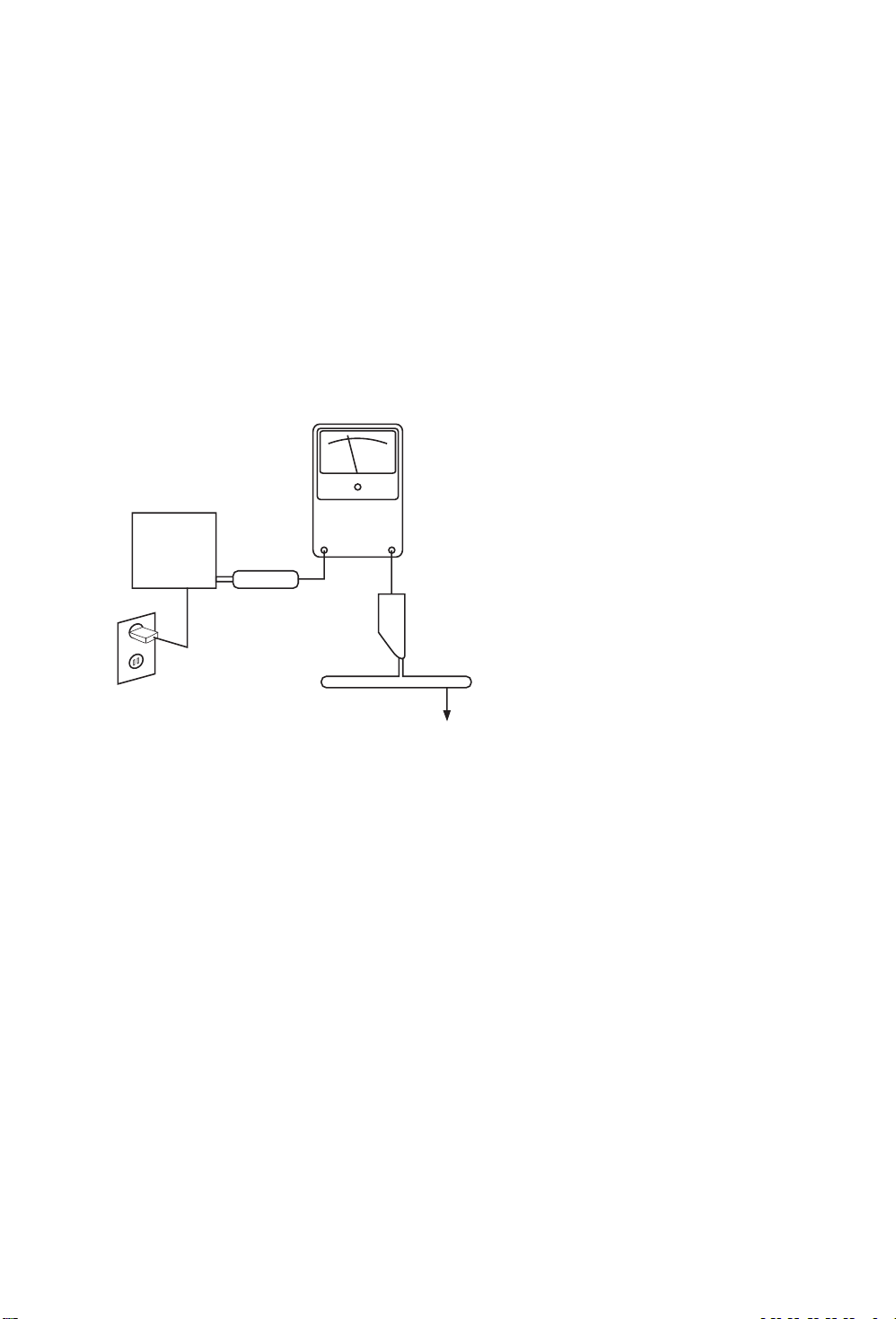
LEAKAGE CURRENT CHECK
Measure leakage current to a known earth ground (water
pipe, conduit, etc.) by connecting a leakage current tester
between the earth ground and all exposed metal parts of the
appliance (input/output terminals, screwheads, metal
overlays, control shaft, etc.). Plug the AC line cord of the
appliance directly into a 120V AC 60Hz outlet and turn the
AC power switch on. Any current measured must not exceed
o.5mA.
Reading should
not be above
0.5mA
Device
under
Leakage
current
tester
test
Test all
exposed metal
surfaces
Also test with
plug reversed
(Using AC adapter
plug as required)
Earth
ground
AC Leakage Test
Page 4

Technical Specifications
harman/kardon
AVR137/230 Service Manual
Page 4 of 87
Audio Section
Stereo Mode
Continuous Average Power (FTC)
40 Watts per channel, 20Hz–20kHz,
@ < 0.07% THD, both channels driven into 8 ohms
Five-Channel Surround Modes
Power Per Individual Channel
Front L&R channels:
30 Watts per channel,
@ < 0.07% THD, 20Hz–20kHz into 8 ohms
Center channel:
30 Watts, @ < 0.07% THD, 20Hz–20kHz into 8 ohms
Surround channels:
30 Watts per channel,
@ < 0.07% THD, 20Hz–20kHz into 8 ohms
Input Sensitivity/Impedance
Linear (High Level) 200mV/47kohms
Signal-to-Noise Ratio (IHF-A) 95dB
Surround System Adjacent Channel Separation
Analog Decoding 40dB
(Pro Logic, etc.)
Dolby Digital (AC-3) 55dB
DTS 55dB
Frequency Response
@ 1W (+0dB, –3dB) 10Hz–100kHz
High Instantaneous
Current Capability (HCC) ±25 Amps
Transient Intermodulation
Distortion (TIM) Unmeasurable
Rise Time 16 µsec
Slew Rate 40V/µsec
FM Tuner Section
Frequency Range 87.5–108MHz
Usable Sensitivity IHF 1.3 µV/13.2dBf
Signal-to-Noise Ratio Mono/Stereo: 70/65dB (DIN)
Distortion Mono/Stereo: 0.15/0.3%
Stereo Separation 35dB @ 1kHz
Selectivity ±400kHz: 70dB
Image Rejection 80dB
IF Rejection 90dB
AM Tuner Section
Frequency Range 522–1620kHz
Signal-to-Noise Ratio 45dB
Usable Sensitivity Loop: 500µV
Distortion 1kHz, 50% Mod: 0.8%
Selectivity ±10kHz: 30dB
Video Section
Video Format PAL/NTSC
Input Level/Impedance 1Vp-p/75 ohms
Output Level/Impedance 1Vp-p /75 ohms
Video Frequency
Response 10Hz–8MHz (–3dB)
General
Power Requirement AC 220-240V/50Hz
Power Consumption 72W idle, 580W maximum
(2 channels driven)
Dimensions (Max)
Width 440mm
Height 165mm
Depth 382mm
Weight 9.6 kg
Depth measurement includes knobs, buttons and terminal connections.
Height measurement includes feet and chassis.
All features and specifications are subject to change without notice.
Harman Kardon is a registered trademark.
*Manufactured under license from Dolby Laboratories.
“Dolby”, “Pro Logic”, and the Double-D symbol are
trademarks of Dolby Laboratories,Inc.
Confidential Unpublished Works. ©1992–1999 Dolby Laboratories, Inc.
All rights reserved.
†
"DTS" and "DTS Neo:6" are registered trademarks of DTS, Inc. "96/24"
is a trademark of DTS, Inc.
Logic 7 is a registered trademark of Lexicon, Inc.
Page 5

Troubleshooting Guide
harman/kardon
AVR137/230 Service Manual
Page 5 of 87
SYMPTOM CAUSE SOLUTION
Unit does not function when • No AC Power • Make certain AC power cord is plugged
Main Power Switch
Display lights, but no sound • Intermittent input connections • Make certain that all input and speaker
or picture connections are secure
Sound is heard, but Front-Panel • Display brightness is turned off • Follow the instructions in the Display Brightness section
Display does not light on page 27 so that the display is set to VFD FULL
No sound from any speaker; • Amplifier is in protection mode • Check speaker-wire connections for shorts at receiver
light around Power switch
No sound from surround or • Incorrect surround mode • Select a mode other than Stereo
center speakers • Incorrect configuration • Check speaker mode
is pushed into a live outlet
• Check to see if outlet is switch controlled
• Mute is on • Press Mute button
• Volume control is down • Turn up volume control
1
is red due to possible short and speaker ends
• Amplifier is in protection mode • Contact your local Harman Kardon service depot
due to internal problems
• Stereo or Mono program material • With (analog or digital) Dolby surround modes, the surround
decoder may not create rear-channel
information from non-encoded programs
• Speakers not properly connected • Check speaker-wire connections or use test tone
to verify connections (see page 20)
Unit does not respond to • Weak batteries in remote • Change remote batteries
remote commands • Wrong device selected • Press the AVR selector
• Remote sensorEis obscured • Make certain front-panel sensor is visible to remote or
connect remote sensor
Intermittent buzzing in tuner • Local interference • Move unit or antenna away from computers, fluorescent lights,
motors or other electrical appliances
Letters flash in the Channel Indicator • Digital audio feed paused • Resume play for DVD
Display and Digital Audio stops • Check that Digital Signal is fed to the Digital Input selected
Processor Reset
In the rare case where the unit’s operation or the
displays seem abnormal, the cause may involve
the erratic operation of the system’s memory or
microprocessor.
To correct this problem, first unplug the unit from
the AC wall outlet and wait at least three
minutes. After the pause,reconnect the AC
power cord and check the unit’s operation.If the
system still malfunctions, a system reset may
clear the problem.
To clear the AVR’s entire system memory
including tuner presets, output level settings,
delay times and speaker configuration data, first
put the unit in Standby by pressing the System
Power Control button
the Surround Mode Button
The unit will turn on automatically. Note that
once you have cleared the memory in this manner,
it is necessary to re-establish all system
configuration settings and tuner presets.
1
. Next, press and hold
6
for 5 seconds.
5
NOTE: Resetting the processor will erase any
configuration settings you have made for
speakers,output levels, surround modes, digital
input assignments as well as the tuner presets.
After a reset the unit will be returned to the
factory presets, and all settings for these items
must be reentered.
If the system is still operating incorrectly,there
may have been an electronic discharge or severe
AC line interference that has corrupted the
memory or microprocessor.
If these steps do not solve the problem, consult
an authorized Harman Kardon service depot.
Page 6
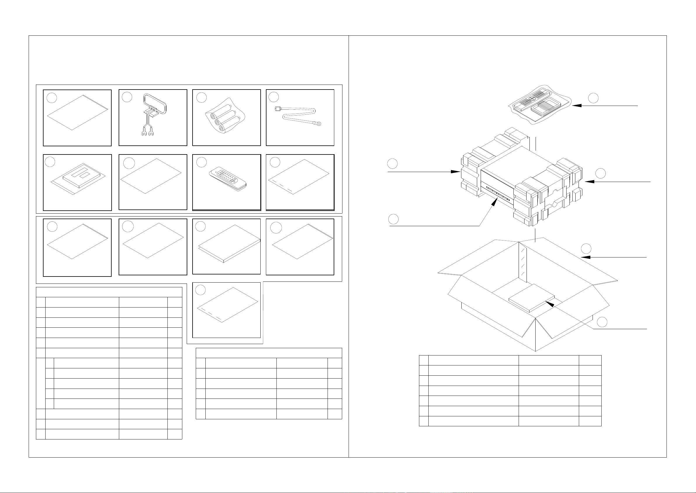
1. Instruction manual ass'y - Accessories
harman/kardon
AVR137/230 Service Manual
Page 6 of 87
AVR 137/230
2. Package Drawing
1
5
9
POLY BAG
COVER ASS'Y
2
AM LOOP ANTENNA ASS'Y
6
IMAGE BROCHURES
10
3
BATTERY ASS'Y
7
REMOCON
TRANSMITTER ASS'Y
11
4
FM 1 POLE ANT
8
STAPLE
12
2
SNOW PAD (L)
SET
4
ACCESSORY-1
1
SNOW PAD (R)
3
BOX ,OUT CARTON
5
POLY BAG
BOOKLET,INFORMATION
ACCESSORY-1
NO
1
2
3
4
5
6
7
8 STAPLE CPL0905 3
DESCRIPTION
POLY BAG
AM LOOP ANTENNA ASS'Y
BATTERY 3
FM 1 POL ANT(UL)
COVER ASS'Y
1
COVER A
2
COVER B
SHEET,FRONT COVER
3
PAD , COVER
4
5
BAG , POLY
IMAGE BROCHURES
REMOCON ASS'Y CARTAVR132/230 1
PARTS NO. Q,ty
CPB1061Y
CSA1A027Z
CABR03P3
CSA1A018Z 1
CGRAVR130/230ZA
CGR1A331M7H43 1
CQE1A220Z
CPS1A676 1
CPB1A176Z 1
HQE1A273Z
MANUAL INSTRUCTION
MANUAL SETUP CODE
13
1
1
STAPLE
1
1
NO
1CGR1A332M7H43
1
1
DESCRIPTION
9
BOOKLET,INFORMATION
10
11
12
MANUAL ,SETUP GUIDE
13
STAPLE CPL0905 3
ACCESSORY-2
PARTS NO. Q,ty
CQE1A180Z 1
CQX1A1154XMANUAL,INSTRUCTION
CQX1A1138Y
DESCRIPTIONNO
ACCESSORY-1
1CPB1061YPOLY BAG
1
1
1
SNOW,PAD(L)
2
3
SNOW,PAD(R)
4
SET
BOX,OUT CARTON5
6
ACCESSORY-2 CQXAVR132/230
CQXAVR132/230
CPS4A564
CPS4A565
AVR132/230SET
CPG1A820T
Q,tyPARTS NO.
1
1
1
1
1
1
ACCESSORY-2
6
Page 7
DISASSEMBLY
harman/kardon
AVR137/230 Service Manual
Page 7 of 87
AVR137/230
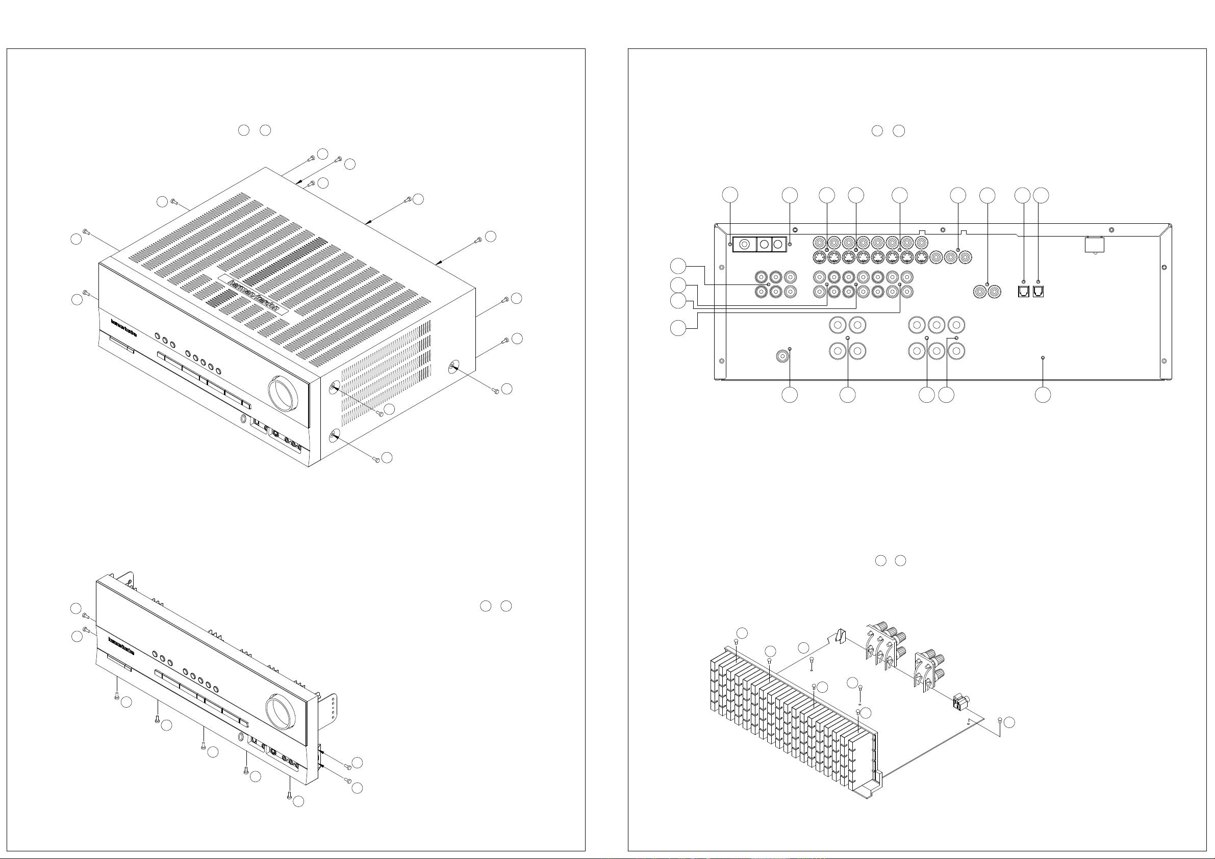
1. Removing the Top Cabinet
Remove the Screws
6
4
5
3. Removing the Rear Panel
13
1
~
10
9
11
7
8
12
13
3
1
Remove the Screws
6
7
8
9
10
14
5
4 3 2 1
15 16 17
18
1
~
13
11
12
18
2
4. Removing the Main PCB
1 7
Remove the Screws
~
2. Removing the Front Panel
9
8
7
6
5
4
Remove the Screws
1
2
3
1 9
~
1
2
5
6
3
4
7
Page 8

DISASSEMBLY PROCEDURES for HK AVR 137
harman/kardon
AVR137/230 Service Manual
Page 8 of 87
<1> TOP-CABINET(21) REMOVAL
1. Remove 13 screws(S1,S7) and then remove the Top-cabinet.
<2> FRONT PANEL ASS’Y REMOVAL
1. Remove the Top-cabinet, referring to the previous step<1>.
2. Disconnect the card cable between connector(CN72-17p) on the Fip PCB(37-1)
and connector(CN72) on the Input PCB(39-1).
3. Disconnect the lead wire(BN81-8P) on the Fip PCB(37-1) from connector(CN81) on the Trans PCB(40-4).
4. Disconnect the lead wire(BN22-6P) on the Phone PCB(37-5) from connector(CN22) on the Input PCB(39-1).
5. Disconnect the lead wire(BN18-5P) on the Phone PCB(37-5) from connector(CN18) on the Input PCB(39-1)
6. Disconnect the lead wire(BN10-4P) on the Volume PCB(37-6) from connector(CN10) on the Input PCB(39-1)
7. Disconnect the lead wire(BN41-6P) on the Volume PCB(37-6) from connector(CN41) on the Video PCB(41)
8. Remove 1 screw(S10) and then lead wire(JW82-1P,JW83-1P) on the Phone PCB(37-5).
9 .Remove 1screw(S10) and then lead wire(JW84-1P) on the Volume PCB(37-3).
10. Remove 10 screws(S1) and then remove the Front Panel ASS’Y.
<3> Volume PCB(37-6) REMOVAL
1. Remove the Top-cabinet, referring to the previous step<1>.
2. Remove the Front Panel ASS’Y, referring to the previous step<2>.
3. Pull out the Volume Knob ASS’Y.
4. Disconnect connector(CN84) on the Volume PCB(37-6) from the lead wire(BN84-5P) on the Fip PCB(37-1).
5. Remove 8 screws(S2,S14), and then remove the Volume PCB(37-6).
<4>PHONE PCB(37-5) REMOVAL
1. Remove the Top-cabinet, referring to the previous step<1>.
2. Remove the Front Panel ASS’Y, referring to the previous step<2>.
3.. Disconnect connector(CN85)on the Phone PCB(37-5) from the lead wire(BN85-2P) on the Fip PCB(37-1).
4. Remove 2 screws(S2) and then remove the Phone PCB(37-5).
.
<5>POWER LED PCB(37-3) REMOVAL
1. Remove the Top-cabinet, referring to the previous step<1>.
2. Remove the Front Panel ASS’Y, referring to the previous step<2>.
3. Disconnect connector(CN88) on the Power Led PCB(37-3) from the lead wire(BN88-4P) on the Fip PCB(37-1) .
4. Remove 2 screws(S2) and then remove the Power led PCB(37-3).
<6>FIP PCB(37-1) REMOVAL
1. Remove the Top-cabinet, referring to the previous step<1>.
2. Remove the Front Panel ASS’Y, referring to the previous step<2>.
3. Disconnect the lead wire(BN84-5P) on the Fip PCB(37-1) from connector(CN84) on the Volume PCB(37-6).
4. Disconnect the lead wire(BN85-2P) on the Fip PCB(37-1) from connector(CN85) on the Phone PCB(37-5).
5. Disconnect the lead wire(BN88-4P) on the Fip PCB(37-1) from connector(CN88) on the Power Led PCB(37-3).
6. Remove 3 screws(S2) and then remove the Guide PCB(37-8) & the Fip PCB(37-1).
<7>TUNER MODULE(42) REMOVAL
1. Remove the Top-cabinet, referring to the previous step<1>.
2. Disconnect the card cable between connector(CON1-13p) on the Tuner module(42)
and connector(CN13) on the Input PCB(39-1).
Page 9

3. Remove 2 screws(S8) and then remove the Tuner Module(42).
harman/kardon
AVR137/230 Service Manual
Page 9 of 87
<8>VIDEO PCB(41) REMOVAL
1. Remove the Top-cabinet, referring to the previous step<1>.
2. Disconnect the card cable between connector(BN14-13p) on the Video PCB(41)
and connector(CN14) on the Input PCB(39-1).
3. Disconnect connector(CN43) on the Video PCB(41)
from the lead wire(BN43-4P) on the Regulator PCB(A)(40-2).
4. Disconnect connector(CN41) on the Video PCB(41) from the lead wire(BN41-6P) on the Volume PCB(37-6).
5. Remove 6 screws(S8) and then remove the Video PCB(41).
<9>INPUT PCB(39-1) REMOVAL
1. Remove the Top-cabinet, referring to the previous step<1>.
2. Remove the Tuner module(42), referring to the previous step<7>
3. Remove the Video PCB(41), referring to the previous step<8>
4. Disconnect connector(CN20) on the the Input PCB(39-1)
from the lead wire(BN20-5P) on the Regulator PCB(B)(40-5).
5. Disconnect connector(CN22) on the Input PCB(39-1) from the lead wire(BN22-6P) on the Phone PCB(37-5).
6. Disconnect connector(CN18) on the Input PCB(39-1) from the lead wire(BN18-5P) on the Phone PCB(37-5)
7. Disconnect connector(CN10) on the Input PCB(39-1) from the lead wire(BN10-4P) on the Volume PCB(37-6).
8. Disconnect the card cable between connector(CN14) on the Input PCB(39-1).
and connector(BN14-9p) on the Video PCB(41).
9. Disconnect the card cable between connector(CN12-21p) on the Input PCB(39-1)
and connector(CN12-21p)) on the main PCB(38-1)
10. Disconnect the card cable between connector(CN11-13p) on the Input PCB(39-1)
and connector(CN11-13p) on the main PCB(38-1)
11. Disconnect connector(CN49) on the Input PCB(39-1) from the lead wire(BN49-5P) on the Rds PCB(39-2).
12. Remove 11 screws(S8,S15) and then remove the Input PCB(39-1).
<10>POWER TRANS(36) & POWER PCB ASS’Y(40) REMOVAL
1. Remove the Top-cabinet, referring to the previous step<1>.
2. Disconnect lead wire of the Power Trans(36) from connector (CN91-3P) on the Main PCB(38-1)
3. Disconnect connector(CN19-3P,CN20-4P) on TRANS PCB(40-3)
from the lead wire(BN19-3P,BN20-4P) on the Main PCB(38-1).
4. Disconnect the lead wire(BN96-8P) on the Power PCB(40-4)
from connector(CN96) on the Regulator PCB(B)(40-5).
5. Disconnect the lead wire(BN99-8P) on the Power PCB(40-4)
from connector(CN99) on the Regulator PCB(A)(40-2).
6. Disconnect connector(CN81) on the Trans PCB(40-4) from the lead wire(BN81-8P) on the Fip PCB(37-1).
7. Remove 4 Trans screws(S9) and then remove the Power Trans(36)& Power PCB ASS’Y(40) REMOVAL .
<11>MAIN PCB ASS’Y(38-1) REMOVAL
1. Remove the Top-cabinet, referring to the previous step<1>.
2. Remove the Tuner module(42), referring to the previous step<7>.
3. Remove the Video PCB(41) referring to the previous step<8>.
5. Remove the Input PCB(39-1), referring to the previous step<9>.
6. Remove the AC Cord(35) on the Main PCB(38-1)
7. Disconnect the lead wire(BN90-2P) on the Main PCB(38-1) from connector(CN86) on Moms PCB(37-4).
Page 10

8. Disconnect connector (CN91-3P) on the Main PCB(38-1) from lead wire of the Power Trans(36)
harman/kardon
AVR137/230 Service Manual
Page 10 of 87
9. Disconnect the lead wire(BN89-2P) on the Main PCB(38-1) from connector(CN89) on Regulator PCB(A)(40-2).
10. Disconnect the lead wire(BN19-3P,BN20-4P) on the Main PCB(38-1)
from connector(CN19-3P,CN20-4P) on TRANS PCB(40-4).
11. Remove 11screws(S13-1EA, S4-2EA, S6-2EA, S8-6EA) and then remove the Main PCB ASS’Y(38-1).
Page 11
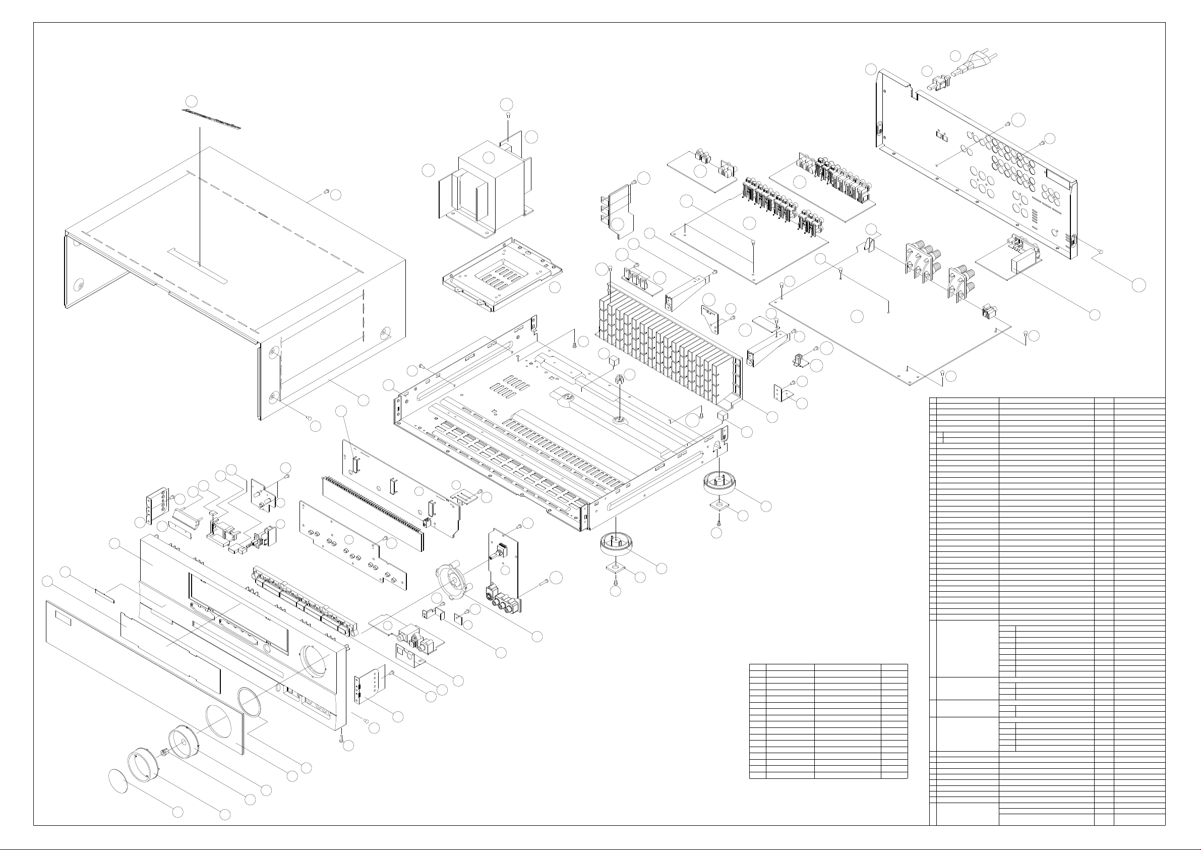
AVR 137/230 EXPLODED VIEW
harman/kardon
AVR137/230 Service Manual
Page 11 of 87
35
33
34
44
S9
S13
40-3
S8
36
40-4
S16
S1
40-5
S5
S15
40-1
39-1
41
32
30
S16
S17
29
40-2
S4
S6
x2
S10
38-2
S4
S5
43
S5
28
22
21
20
S7
37-3
37-4
S2
37-1
37-8
S2
S2
37-2
S2
37-6
S14
S2
23
S4
15
13
14-1
14
S2
10
12
9
8
7
S10
S4
24
S2
37-5
37-9
19
16
17
11
S2
10
S1
S1
6
5
39-2
23
S4
S5
S14
40-2
S5
27
26
25
24
DESCRIPTION PARTS NO. Q,ty
NO
S1
S2
S3
S4
S5
S6
S7
S8
S9
S10
S11
S12
S13
S14
S15
S16
S17
SCREW
SCREW
SCREW
SCREW
SCREW
SCREW
SCREW
SCREW,TRANS
SCREW
SCREW
SCREW
SCREW,SPECIAL
SCREW,SPECIAL
SCREW,SPECIAL
CTB3+10GR
CTWS3+10GR
CTW3+8JR
CTB3+8JR
CTW3+12JR
CTB4+6FFC
CTB3+10GFZR
CHD1A023R
CTB3+6JR
CTB3+16GFZR
CTB3+8JFZR
CHD1A012R
CHD1A012ZR
CHD3A012R
CHD4A012R
38-1
42
S4
S4
DESCRIPTION
NO
ORNAMENT,VOLUME CGU1A318Z 1
1
CAP,VOLUME
2
HOLDER,VOLUME
3
INDICATOR,VOLUME
4
WINDOW ASS'Y
5
WINDOW,FIP CGU2A399Z
1
BADGE,MODEL
2
6
FILTER,FIP
7
BDAGE,HARMAN/KARDON
8
PANEL,FRONT
9
BRACKET,SIDE
10
KNOB,FUNCTION
11
SHEET,REFLECTION CMZ1A120 1
12
KNOB,POWER
13
INDICATOR,POWER
14
KNOB,MOMS
15
BRACKET,PCB CMK2A010
16
PLATE,SHIELD
17
18
HOLDER,LED
19
BRACKET,FIP
20
CABINET,TOP
21
CHASSIS,BOTTOM
22
RUBBER,CUSHION
23
FOOT
24
SUPPORT,CUSHION
25
HEAT SINK
26
BRACKET,PCB
27
HOLDER,PCB
28
BRACKET,TRANS
29
BRACKET,PCB(H/T)
30
BRACKET,PCB CMD1A570 1
31
BRACKET,PCB
32
PANEL,REAR
33
BUSHING,AC CORD
34
CORD,POWER
35
TRANS,POWER
36
FRONT PAB ASS'Y
37
13CTB3+8JFCSCREW
31
1
9
10
3
6
22
4
19
2
3
16
2SCREW,SPECIAL
6
5
MAIN PCB ASS'Y COP11911H 1
38
INPUT PCB ASS'Y COP11931H 1
39
POWER PCB ASS'Y
40
VIDEO PCB ASS'Y
41
TUNER MODULE
42
43
BADGE,HARMAN/KARDON CGB1A152Z
44
PARTS NO.
CGX1A338MBC63
CMH1A214
CGL1A222
CGUAVR132/230
CGB1A173Z
CMZ2A090SHEET,VOLUME 1
CMZ1A088
KGB1A158Z
CGW1A427RDZH43
CMD2A443
CBT1A1028MBYG27
CBT1A1026MMZG27
CGL1A258Z
CBC1A158MBZG27
CMC1A302
CMH1A215
CMD1A209
CKC4B145S46Z
CUA2A229
CHG1A329
CKL2A069H43
CHG1A104Z
CMY1A273
CMD1A417
CHE1A170
CMD1A487
CMD1A398
CMD1A387
CKF8A319Z
KHR1A028
CJA523FBYA
CLT5U026ZE
COP11910H
FIP PCB
37-1
KEY PCB
37-2
POWER LED PCB
37-3
MOMS PCB
37-4
PHONE PCB
37-5
VOLUME PCB
37-6
RS232 PCB
37-7
GUIDE PCB(CARD CABLE)
37-8
MAIN PCB
38-1
GUIDE PCB(CARD CABLE) 1
38-2
INPUT PCB
39-1
RDS PCB 1
39-2
COP11916H 1
DIGITAL IN PCB 1
40-1
REGULATOR PCB(A) 5
40-2
TRANS PCB 1
40-3
TRANS PCB 1
40-4
REGULATOR PCB(B) 1
40-5
COP11930H 1
CNVM9014MS171L
CHG1A160ZCUSHION
Q,ty
Weright
1
1
1
1
1
1
1
1
1
2
11
1
1
1
1
1
1
3
1
1
4
4
1
1
2
2
1
2
2
1
1
1
1
1
1
1
1
1
1
1
1
1
1
1
1
1
1
1
4
3
1
2
Page 12
AVR137/230 Electrical Parts List
H
E
harman/kardon
AVR137/230 Service Manual
Page 12 of 87
Ref. # Part Number
CGB1A152Z BADGE , HARMAN/KARDON(TOP) BADGE 1
CGL1A222 INDICATOR , VOLUME INDICATOR 1
CGUAVR137 FRONT WINDOW ASS'Y ASS'Y 1
CGB1A183Z BADGE , HARMAN AVR137/230 BADGE 1
CGU2A399Y WINDOW , FIP FIP WINDOW 1
CGU1A318Z ORNAMENT , VOLUME ORANMENT 1
CGX1A338MBC CAP , VOLUME CAP 1
CKC4B145S46 CABINET , TOP TOP CABINET 1
BKC4C145S46 SHEET , CABINET(350X750) TOP CABINET 1
CLZ9Z028Z FERRITE CORE(21.2X6.4X12.7) FERRITE CORE 1
CMH1A214 HOLDER , VOLUME HOLDER 1
CMZ2A090 SHEET , VOLUME SHEET 1
CQB1A549Y LABEL , ATTENTION DVD48 LABEL 1
CQB1A551Z LABEL , BAR CODE LABEL 1
CQB1A622 LABEL , SERIAL NO LABEL 1
CRE1A037 LOCKER LOCKER 10
CTB3+8JFC SCREW SCREW 13
CTB4+6FFC SCREW SCREW 6
CHE154 CLAMPER , ARM ASS'Y 0,12
CPG1A822S BOX , OFFSET CARTON BOX 1
CPS5A564 PAD , SNOW L SNOW PAD 1
CPS5A565 PAD , SNOW R SNOW PAD 1
CQB1A551Z LABEL , BAR CODE LABEL 2
CQB1A649Z LABEL , COUNTRY LABEL 2
CQS1A001 RIBON , BAR CODE SONY(TR-4070) 0,12
CQXAVR137 INSTRUCTION MANUAL ASS'Y ASS'Y 1
CABR03P3 BATTERY (SIZE 'AAA') 3PCS IN 1 BATTERY 3
CARTAVR137/ REMOCON TRANSMITTER ASS'Y ASS'Y 1
CGRAVR130/2 COVER ASS'Y COVER 1
CGR1A331M7H COVER A COVER 1
CGR1A332M7H COVER B COVER 1
CPS1A676 PAD , COVER PAD 1
CQE1A220Z SHEET , FRONT COVER SHEET 1
CQE1A180Z BOOKLET , IMFORMATIONS CARD 1
CQX1A1256Z MANUAL , SET UP AVR147/230 MANUAL 1
CQX1A1260Z MANUAL , INSTRUCTION AVR137/230 MANUAL 1
CSA1A018Z FM 1 POLE ANT ANT 1
CSA1A027Z AM LOOP ANT ANT 1
HQE1A273Z HARMAN IMAGE BROCHURES BROCHURES 1
Description
Value Qty
Ref. # Part Number
CGWAVR137/2 FRONT PANEL ASS'Y ASS'Y 1
CBC1A158MBZ KNOB , MOMS KNOB 1
CBT1A1026MM KNOB , POWER KNOB 1
CBT1A1028MB KNOB , FUNCTION KNOB 1
CGL1A258Z INDICATOR , POWER INDICATOR 1
CGW1A427RDZ PANEL , FRONT PANEL 1
CHR301 CLAMPER CLAMPER 13
CMC1A302 PLATE , SHIELD PLATE 1
CMD2A443 BRACKET , SIDE BRACKET 2
CMH2A215 HOLDER , LED AVR350 HOLDER 1
CMK2A010 BRACKET , PCB BRACKET 1
CMZ1A088 FILTER , FIP FIP FILTER 1
CMZ1A120 SHEET , REFLECTION SHEET 1
CTB3+10GR SCREW SCREW 31
CTB3+16GFZR SCREW SCREW 2
KGB1A158Z BADGE , HARMAN/KARDON(FRONT) BADGE 1
CB72 CWC1B2A17A2 WAFER, CARD CABLE (1mm PITCH,B TYPE) WAFER 1
Ref. # Part Number
COP11910H FRONT PCB ASS`Y ASS'Y 1
CMC3A111 PLATE , EART
Description
Description
Value Qty
Value Qty
PLAT
1
Page 13

C714 HCBS1H151KB CAP , CERAMIC 150UF 50V K 1
N
harman/kardon
AVR137/230 Service Manual
Page 13 of 87
C716 CCEA1AH331T CAP , ELECT 330UF 10V 1
C719 HCBS1H102KB CAP , CERAMIC 1000PF 50V K 1
C720 HCBS1H102KB CAP , CERAMIC 1000PF 50V K 1
C721 HCBS1H102KB CAP , CERAMIC 1000PF 50V K 1
C723 HCBS1H104ZF CAP , CERAMIC 0.1UF 50V Z 1
C728 HCBS1H104ZF CAP , CERAMIC 0.1UF 50V Z 1
C729 HCBS1H473ZF CAP , CERAMIC 0.047UF 50V Z 1
C731 CCEA1HH100 CAP , ELECT 10UF 50V 1
C735 CCEA1CKS100 CAP , ELECT 10UF 16V 1
C742 HCBS1H223ZF CAP , CERAMIC 0.02UF 50V Z 1
C793 HCBS1H104ZF CAP , CERAMIC 0.1UF 50V Z 1
C794 HCBS1C222MX CAP , CERAMIC 2200PF 16V 1
C795 HCBS1H102KB CAP , CERAMIC 1000PF 50V K 1
C796 HCBS1H102KB CAP , CERAMIC 1000PF 50V K 1
C805 HCBS1H223ZF CAP , CERAMIC 0.022UF 50V Z 1
C806 HCBS1H223ZF CAP , CERAMIC 0.022UF 50V Z 1
C807 HCBS1H104ZF CAP , CERAMIC 0.1UF 50V Z 1
C808 HCBS1H181KB CAP , CERAMIC 180PF 50V Z 1
C809 CCEA1AH471T CAP , ELECT 470UF 10V 1
C812 HCBS1H104ZF CAP , CERAMIC 0.1UF 50V Z 1
C817 HCBS1H100JC CAP , CERAMIC 10PF 50V 1
C841 CCEA1HH100T CAP , ELECT 10UF 50V 1
C842 CCEA1HH100T CAP , ELECT 10UF 50V 1
C843 CCEA1HH100T CAP , ELECT 10UF 50V 1
C850 HCBS1H471KB CAP , CERAMIC 470PF 50V 1
C851 HCBS1H471KB CAP , CERAMIC 470PF 50V 1
C852 HCBS1H104ZF CAP , CERAMIC 0.1UF 50V Z 1
C855 HCBS1H101KB CAP , CERAMIC 100PF 50V K 1
C856 HCBS1H101KB CAP , CERAMIC 100PF 50V K 1
C857 HCBS1H104ZF CAP , CERAMIC 0.1UF 50V Z 1
C862 HCBS1H101KB CAP , CERAMIC 100PF 50V K 1
C863 HCBS1H101KB CAP , CERAMIC 100PF 50V K 1
C866 CCEA1HKS100 CAP , ELECT 10UF 50V SMALL SIZE 1
C867 CCEA1HKS100 CAP , ELECT 10UF 50V SMALL SIZE 1
C868 CCEA1EKS470 CAP , ELECT 47UF 25V 1
C869 CCEA1EKS470 CAP , ELECT 47UF 25V 1
C870 HCBS1H681KB CAP , CERAMIC 680PF 50V K 1
C871 HCBS1H681KB CAP , CERAMIC 680PF 50V K 1
C872 CCEA1CH331T CAP , ELECT 330UF 16V 1
C873 CCEA1CH331T CAP , ELECT 330UF 16V 1
C874 HCBS1H101KB CAP , CERAMIC 100PF 50V K 1
C882 HCBS1H104ZF CAP , CERAMIC 0.1UF 50V Z 1
C889 HCBS1H104ZF CAP , CERAMIC 0.1UF 50V Z 1
C891 HCBS1H223ZF CAP , CERAMIC 0.023UF 50V Z 1
C892 HCBS1H223ZF CAP , CERAMIC 0.023UF 50V Z 1
C893 HCBS1H223ZF CAP , CERAMIC 0.023UF 50V Z 1
C894 CCEA1CKS100 CAP , ELECT 10UF 16V 1
C896 HCBS1H223ZF CAP , CERAMIC 0.023UF 50V Z 1
C897 CCEA1AH471T CAP , ELECT 470UF 10V 1
C901 HCBS1H390JT CAP , CERAMIC 39PF 50V Z 1
C903 CCEA1HKS2R2 CAP , ELECT 2.2UF 50V 1
C905 CCEA1HKS2R2 CAP , ELECT 2.2UF 50V 1
D730 CVD1SS133MT DIODE 1SS133 1
D774 CVD1SS133MT DIODE 1SS133 1
D778 HVD1N5819T DIODE , SCHOTTKY 1N5819 1
D784 CVD1SS133MT DIODE 1SS133 1
D785 CVD1SS133MT DIODE 1SS133 1
L702 HLQ02C100KT COIL , AXAIL 10uH 1
Q701 HVTKRC107MT T.R KRC107M 1
Q722 HVTKRA107MT T.R KRA107M 1
Q724 HVTKRC107MT T.R KRC107M 1
Q725 HVTKRC107MT T.R KRC107M 1
Q734 HVTKTC2874B T.R , MUTE KTC2874B 1
Q735 HVTKTC2874B T.R , MUTE KTC2874B 1
Q736 HVTKTC2874B T.R , MUTE KTC2874B 1
Q737 HVTKTC2874B T.R , MUTE KTC2874B 1
Q738 HVTKRC107MT T.R KRC107M 1
Q739 HVTKTA1271Y T.R KTA1271Y 1
R701 CRD20TJ103T RES , CARBO
10K OHM 1/5W J 1
Page 14

R704 CRD20TJ100T RES , CARBON 10 OHM 1/5W J 1
N
harman/kardon
AVR137/230 Service Manual
Page 14 of 87
R705 CRD20TJ820T RES , CARBON 82 OHM 1/5W J 1
R706 CRD20TJ820T RES , CARBON 82 OHM 1/5W J 1
R708 CRD20TJ820T RES , CARBON 82 OHM 1/5W J 1
R709 CRD20TJ470T RES , CARBON 47 OHM 1/5W J 1
R710 CRD20TJ470T RES , CARBON 47 OHM 1/5W J 1
R711 CRD20TJ470T RES , CARBON 47 OHM 1/5W J 1
R718 CRD20TJ222T RES , CARBON 2.2K OHM 1/5W J 1
R737 CRD20TJ100T RES , CARBON 10 OHM 1/5W J 1
R747 CRD20TJ103T RES , CARBON 10K OHM 1/5W J 1
R753 CRD20TF1001 RES , CARBON 1K /1/5W /F 1
R754 CRD20TF1501 RES , CARBON 1.5K /1/5W /F 1
R755 CRD20TF1801 RES , CARBON 1.8K /1/5W /F 1
R756 CRD20TF2701 RES , CARBON 2.7K /1/5W/F 1
R757 CRD20TF3301 RES , CARBON 3.3K /1/5W/F 1
R758 CRD20TF5601 RES , CARBON(5.6K/F) 5.6K/1/5W/F 1
R759 CRD20TF1001 RES , CARBON 1K /1/5W /F 1
R760 CRD20TF1501 RES , CARBON 1.5K /1/5W /F 1
R761 CRD20TF1801 RES , CARBON 1.8K /1/5W /F 1
R762 CRD20TF2701 RES , CARBON 2.7K /1/5W/F 1
R763 CRD20TF3301 RES , CARBON 3.3K /1/5W/F 1
R764 CRD20TF5601 RES , CARBON(5.6K/F) 5.6K/1/5W/F 1
R765 CRD20TF7501 RES , CARBON (7.5K/F) 7.5K/1/5W/F 1
R766 CRD20TF1001 RES , CARBON 1K /1/5W /F 1
R767 CRD20TF1501 RES , CARBON 1.5K /1/5W /F 1
R768 CRD20TF1801 RES , CARBON 1.8K /1/5W /F 1
R769 CRD20TF2701 RES , CARBON 2.7K /1/5W/F 1
R781 CRD20TJ102T RES , CARBON 1K OHM 1/5W J 1
R783 CRD20TJ102T RES , CARBON 10K OHM 1/5W J 1
R784 CRD20TJ102T RES , CARBON 1K OHM 1/5W J 1
R786 CRD20TJ152T RES , CARBON 1.5K OHM 1/5W J 1
R787 CRD20TJ101T RES , CARBON 100 OHM 1/5W J 1
R791 CRD20TJ822T RES , CARBON 8.2K OHM 1/5W J 1
R805 CRD20TJ104T RES , CARBON 100K OHM 1/5W J 1
R806 CRD20TJ472T RES , CARBON 4.7K OHM 1/5W J 1
R824 CRD20TJ221T RES , CARBON 220 OHM 1/5W J 1
R825 CRD20TJ681T RES , CARBON 680 OHM 1/5W J 1
R828 CRD20TJ221T RES , CARBON 220 OHM 1/5W J 1
R829 CRD20TJ681T RES , CARBON 680 OHM 1/5W J 1
R864 CRD20TJ272T RES , CARBON 2.7K OHM 1/5W J 1
R865 CRD20TJ101T RES , CARBON 100 OHM 1/5W J 1
R866 CRD20TJ272T RES , CARBON 2.7K OHM 1/5W J 1
R869 CRD20TJ750T RES , CARBON 75 OHM 1/5W J 1
R871 CRD20TJ104T RES , CARBON 100K OHM 1/5W J 1
R872 CRD20TJ104T RES , CARBON 100K OHM 1/5W J 1
R873 CRD20TJ471T RES , CARBON 470 OHM 1/5W J 1
R874 CRD20TJ471T RES , CARBON 470 OHM 1/5W J 1
R875 CRD20TJ103T RES , CARBON 10K OHM 1/5W J 1
R876 CRD20TJ750T RES , CARBON 75 OHM 1/5W J 1
R877 CRD20TJ750T RES , CARBON 75 OHM 1/5W J 1
R878 CRD20TJ750T RES , CARBON 75 OHM 1/5W J 1
R892 CRD20TJ222T RES , CARBON 2.2K OHM 1/5W J 1
R893 CRD20TJ333T RES , CARBON 33K OHM 1/5W J 1
R895 CRD20TJ101T RES , CARBON 100 OHM 1/5W J 1
R896 CRD20TJ101T RES , CARBON 100 OHM 1/5W J 1
R897 CRD20TJ101T RES , CARBON 100 OHM 1/5W J 1
R898 CRD20TJ101T RES , CARBON 100 OHM 1/5W J 1
R899 CRD20TJ104T RES , CARBON 100K OHM 1/5W J 1
R900 CRD20TJ104T RES , CARBON 100K OHM 1/5W J 1
R901 CRD20TJ152T RES , CARBON 1.5K OHM 1/5W J 1
R902 CRD20TJ152T RES , CARBON 1.5K OHM 1/5W J 1
R903 CRD20TJ102T RES , CARBON 1K OHM 1/5W J 1
R904 CRD20TJ102T RES , CARBON 1K OHM 1/5W J 1
R905 CRD20TJ104T RES , CARBON 100K OHM 1/5W J 1
R906 CRD20TJ104T RES , CARBON 100K OHM 1/5W J 1
R907 CRD20TJ472T RES , CARBON 4.7K OHM 1/5W J 1
R908 CRD20TJ472T RES , CARBON 4.7K OHM 1/5W J 1
R909 CRD20TJ221T RES , CARBON 220 OHM 1/5W J 1
R910 CRD20TJ221T RES , CARBON 220 OHM 1/5W J 1
R911 CRD20TJ221T RES , CARBO
220 OHM 1/5W J 1
Page 15

R912 CRD20TJ221T RES , CARBON 220 OHM 1/5W J 1
T
N
harman/kardon
AVR137/230 Service Manual
Page 15 of 87
R913 CRD20TJ102T RES , CARBON 1K OHM 1/5W J 1
R915 CRD20TJ473T RES , CARBON 47K OHM 1/5W J 1
R918 CRD20TJ472T RES , CARBON 4.7K OHM 1/5W J 1
R919 CRD20TJ472T RES , CARBON 4.7K OHM 1/5W J 1
S701 HST1A020ZT SW , TACT 1A020 1
S702 HST1A020ZT SW , TACT 1A020 1
S703 HST1A020ZT SW , TACT 1A020 1
S704 HST1A020ZT SW , TACT 1A020 1
S705 HST1A020ZT SW , TACT 1A020 1
S706 HST1A020ZT SW , TACT 1A020 1
S707 HST1A020ZT SW , TACT 1A020 1
S711 HST1A020ZT SW , TACT 1A020 1
S712 HST1A020ZT SW , TACT 1A020 1
S713 HST1A020ZT SW , TACT 1A020 1
S714 HST1A020ZT SW , TACT 1A020 1
S715 HST1A020ZT SW , TACT 1A020 1
BK71 CMD1A209 BRACKET , FLT BRACKET 1
BK72 CMD1A209 BRACKET , FLT BRACKET 1
BK73 CMD1A209 BRACKET , FLT BRACKET 1
BN10 CWZAVR230BN WIRE ASS'Y (SHIELD) WIRE 1
BN18 CWZAVR125BN WIRE ASS'Y (SHIELD) WIRE 1
BN22 CWZAVR145BN WIRE ASS'Y (SHIELD) WIRE 1
BN41 CWZAVR130BN WIRE ASS'Y (SHIELD) WIRE 1
BN81 CWB2C908200 WIRE ASS'Y WIRE 1
BN84 CWB2B905080 WIRE ASS'Y WIRE 1
BN85 CWB2B902100 WIRE ASS'Y ( ANGLE ) WIRE 1
BN88 CWB2B904100 WIRE ASS'Y WIRE 1
BN89 CWB2B904100 WIRE ASS'Y WIRE 1
CN72 CJP17GA193Z WAFER, CARD CABLE (SMD) WAFER 1
CN84 CJP05GB46ZY WAFER WAFER 1
CN85 CJP02GA19ZY WAFER , 2PIN WAFER 1
CN86 CJP02GA89ZM WAFER WAFER 1
CN88 CJP04GB46ZY WAFER WAFER 1
CN89 CJP04GB46ZY WAFER WAFER 1
D701 CVD52CSBBCE L.E.D , BLUE L.E.D 1
D703 CVD52CSBBCE L.E.D , BLUE L.E.D 1
D705 CVD52CSBBCE L.E.D , BLUE L.E.D 1
D723 CVD50BOBBWG L.E.D , 2 COLOR (ORG , BLUE) L.E.D 1
D727 CVD50BOBBWG L.E.D , 2 COLOR (ORG , BLUE) L.E.D 1
ET03 CMD1A569 BRACKET , PCB BRACKET 1
FIP1 HFLHCA18ML0 F.I.P F.I.P 1
IC73 HRVNJL34H38 SENSOR , REMOCON JRC 1
IC75 HVI74ACT04M I.C , HEX FAIRCHILD 1
IC76 HVI74HCU04A I.C , INVERTER TOSHICA 1
IC86 HVINJM4556A I.C , HEADPHONE JRC 1
JK81 CJJ4M043Y JACK , BOARD JACK 1
JK82 HJSTORX177L MODULE , OPTICAL(RX) OPT JACK(RX) 1
JK83 CJJ2E026Z JACK , HEADPHONE(SILVER PLATE) JACK 1
JK85 CJJ9M003Z JACK , S-VIDEO JACK 1
JK86 CJJ4S023Y JACK , BOARD JACK 1
JW82 CWE8202300R WIRE ASS'Y WIRE 1
JW83 CWE8202150R WIRE ASS'Y WIRE 1
JW84 CWE8202110R WIRE ASS'Y WIRE 1
SW1 CSH1A008ZV SW , PUSH (MOMS) SWITCH 1
VR74 CSR2A037Z ENCODER ENCODER 1
Ref. # Part Number
CUAAVR137/2 BOTTOM CHASSIS ASS'Y ASS'Y 1
CHD1A012ZR SCREW , SPECIAL SCREW 2
CHD1A023R SCREW , SPECIAL SCREW 4
CHD4A012R SCREW , SPECIAL SCREW 5
CHE170 HOLDER , PCB HOLDER 2
CHE36-3 CLAMPER , WIRE CLAMPER 1
CHG1A104Z CUSHUON , RUBBER CUSHION 1
CHG1A160Z CUSHION , RUBBER CUSHION 1
CHG1A360 CUSHION , FOO
Description
CUSHIO
Value Qty
4
Page 16
CHS1A032 TAPE , HEMELON TAPE 4
T
harman/kardon
AVR137/230 Service Manual
Page 16 of 87
CJA2B043ZA CORD , POWER(EUR) POWER CORD 1
CKF8A319W PANEL , REAR AVR137/230 REAR PANEL 1
CKL2A069H43 FOOT FOOT 4
CLZ9W003Z FERRITE , RING FERRITE RING 1
CMD2A487 BRACKET , TRANS BRACKET 1
CNVM9014MS1 MODULE , TUNER(EUR) TUNER 1
CQB1A173Y LABEL, FUSE CAUTION LABEL 1
CTB3+10GFZR SCREW SCREW 17
CTB3+6JR SCREW SCREW 13
CTB3+8JFZR SCREW SCREW 1
CTB3+8JR SCREW SCREW 7
CTW3+12JR SCREW SCREW 2
CTW3+8JR SCREW SCREW 8
CUA3A229 CHASSIS , BOTTOM AVR350/230 CHASSIS 1
C2K26161 SOLDER, WIRE SOLDER, WIRE 5
CB11 CWC1B2A13A1 CABLE , CARD CARD CABLE 1
CB12 CWC1C4A21B1 CABLE , CARD CARD CABLE 1
CB13 CWC1C4A13B0 CABLE , CARD CARD CABLE 1
CB14 CWC1B2A09A1 WAFER, CARD CABLE (1mm PITCH,B TYPE) WAFER 1
F901 KBA2C4000TL FUSE LITTLE FUSE 1
T901 CLT5U026ZE TRANS, POWER MAIN TRANS 1
KHR1A028 BUSHING , AC CORD AC CORD 1
Ref. # Part Number
COP11911H MAIN PCB ASS'Y ASS'Y 1
CHD3A012R SCREW , SPECIAL SCREW 3
CTW3+8JR SCREW SCREW 2
C8AGB288 BOND (MAX) BOND 10,2
CUP11911W PCB, MAIN AVR350/230(330X247,FR-1) PCB 1
C501 CCEA1HH100T CAP , ELECT 10UF 50V 1
C502 CCEA1HH100T CAP , ELECT 10UF 50V 1
C503 CCEA1HH100T CAP , ELECT 10UF 50V 1
C504 CCEA1HH100T CAP , ELECT 10UF 50V 1
C505 CCEA1HH100T CAP , ELECT 10UF 50V 1
C506 CCKT1H331KB CAP , CERAMIC 330PF 50V 1
C507 HCBS1H331KB CAP , CERAMIC 330PF 50V 1
C508 HCBS1H331KB CAP , CERAMIC 330PF 50V 1
C509 CCKT1H331KB CAP , CERAMIC 330PF 50V 1
C510 HCBS1H331KB CAP , CERAMIC 330PF 50V 1
C561 CCEA1CH101T CAP , ELECT 100UF 16V 1
C562 CCEA1CH101T CAP , ELECT 100UF 16V 1
C563 CCEA1CH101T CAP , ELECT 100UF 16V 1
C564 CCEA1CH101T CAP , ELECT 100UF 16V 1
C565 CCEA1CH101T CAP , ELECT 100UF 16V 1
C566 CCEA1CH101T CAP , ELECT 100UF 16V 1
C567 CCEA1CH101T CAP , ELECT 100UF 16V 1
C568 CCEA1CH101T CAP , ELECT 100UF 16V 1
C569 CCEA1CH101T CAP , ELECT 100UF 16V 1
C570 CCEA1CH101T CAP , ELECT 100UF 16V 1
C571 HCBS1H681KB CAP , CERAMIC 680PF 50V 1
C572 HCBS1H681KB CAP , CERAMIC 680PF 50V 1
C573 HCBS1H681KB CAP , CERAMIC 680PF 50V 1
C574 HCBS1H681KB CAP , CERAMIC 680PF 50V 1
C575 HCBS1H681KB CAP , CERAMIC 680PF 50V 1
C601 CCCT1H120JC CAP , CERAMIC 12PF 50V 1
C602 CCCT1H120JC CAP , CERAMIC 12PF 50V 1
C603 CCCT1H120JC CAP , CERAMIC 12PF 50V 1
C604 CCCT1H120JC CAP , CERAMIC 12PF 50V 1
C605 CCCT1H120JC CAP , CERAMIC 12PF 50V 1
C606 CCCT1H330JC CAP , CERAMIC 33PF 50V 1
C607 CCCT1H330JC CAP , CERAMIC 33PF 50V 1
C608 CCCT1H330JC CAP , CERAMIC 33PF 50V 1
C609 CCCT1H330JC CAP , CERAMIC 33PF 50V 1
C610 CCCT1H330JC CAP , CERAMIC 33PF 50V 1
C681 CCEA1HH100T CAP , ELECT 10UF 50V 1
C682 CCEA1HH100T CAP , ELEC
Description
Value Qty
10UF 50V 1
Page 17

C683 CCEA1HH100T CAP , ELECT 10UF 50V 1
harman/kardon
AVR137/230 Service Manual
Page 17 of 87
C684 CCEA1HH100T CAP , ELECT 10UF 50V 1
C685 CCEA1HH100T CAP , ELECT 10UF 50V 1
C726 CCKT1H221KB CAP , CERAMIC 220PF 50V 1
C900 HCQI1H473JZ CAP , MYLAR 0.047UF 50V 1
C901 HCQI1H473JZ CAP , MYLAR 0.047UF 50V 1
C905 CCFT1H223ZF CAP , CERAMIC 0.022UP 50V 1
C907 CCEA1CH101T CAP , ELECT 100UF 16V 1
C908 CCFT1H223ZF CAP , CERAMIC 0.1UF 50V ZF 1
C910 HCQI1H473JZ CAP , MYLAR 0.047UF 50V 1
C911 CCEA1CH471T CAP , ELECT 470UF 16V 1
C912 CCEA1EH221T CAP , ELECT 220UF 16V 1
C913 CCFT1H104ZF CAP , SEMICONDUCTOR 0.1UF 50V ZF 1
C914 HCQI1H473JZ CAP , MYLAR 0.047UF 50V J 1
C917 HCQI1H473JZ CAP , MYLAR 0.047UF 50V J 1
C924 CCFT1H104ZF CAP , SEMICONDUCTOR 0.1UF 50V ZF 1
C939 CCEA1HH4R7T CAP , ELECT 4.7UF 50V 1
C940 CCEA1AH471T CAP , ELECT 470UF 10V 1
C948 CCFT1H104ZF CAP , SEMICONDUCTOR 0.1UF 50V ZF 1
C949 CCEA1HH220T CAP , ELECT 22UF 50V 1
C971 HCQI1H562JZ CAP , MYLAR 5600PF 50V 1
C972 HCQI1H562JZ CAP , MYLAR 5600PF 50V 1
C973 HCQI1H562JZ CAP , MYLAR 5600PF 50V 1
C980 HCQI1H562JZ CAP , MYLAR 5600PF 50V 1
C981 HCQI1H562JZ CAP , MYLAR 5600PF 50V 1
C990 HCQI1H473JZ CAP , MYLAR 0.047UF 50V J 1
C991 CCEA1HH1R0T CAP , ELECT 1UF 50V 1
C992 HCQI1H473JZ CAP , MYLAR 0.047UF 50V J 1
C993 HCQI1H473JZ CAP , MYLAR 0.047UF 50V J 1
C995 HCQI1H473JZ CAP , MYLAR 0.047UF 50V J 1
C997 HCQI1H473JZ CAP , MYLAR 0.047UF 50V J 1
C999 CCFT1H223ZF CAP , CERAMIC 0.022UF 50V ZF 1
D501 CVD1SS133MT DIODE 1SS133 1
D502 CVD1SS133MT DIODE 1SS133 1
D503 CVD1SS133MT DIODE 1SS133 1
D504 CVD1SS133MT DIODE 1SS133 1
D505 CVD1SS133MT DIODE 1SS133 1
D581 CVD1SS133MT DIODE 1SS133 1
D582 CVD1SS133MT DIODE 1SS133 1
D583 CVD1SS133MT DIODE 1SS133 1
D584 CVD1SS133MT DIODE 1SS133 1
D585 CVD1SS133MT DIODE 1SS133 1
D901 CVD1N4003SR DIODE , RECT 1N4003 1
D902 CVD1SS133MT DIODE 1SS133 1
D911 CVD1SS133MT DIODE 1SS133 1
D912 CVD1SS133MT DIODE 1SS133 1
D914 CVD1SS133MT DIODE 1SS133 1
D917 CVD1SS133MT DIODE 1SS133 1
D953 CVD1SS133MT DIODE 1SS133 1
D954 CVD1N4003SR DIODE , RECT 1N4003 1
D955 CVD1N4003SR DIODE , RECT 1N4003 1
D956 CVD1N4003SR DIODE , RECT 1N4003 1
D957 CVD1N4003SR DIODE , RECT 1N4003 1
D961 CVD1N4003ST DIODE , RECT 1N4003 1
D962 CVD1N4003SR DIODE , RECT 1N4003 1
D963 CVD1N4003ST DIODE , RECT 1N4003 1
D973 CVD1SS133MT DIODE 1SS133 1
D974 CVD1SS133MT DIODE 1SS133 1
D979 HVDMTZJ62BT DIODE , ZENER MTZJ6.2B 1
D980 CVD1SS133MT DIODE 1SS133 1
ET90 HJT1A025 PALTE , EARTH MET37-0002 1
ET91 HJT1A025 PALTE , EARTH MET37-0002 1
F901 KJCFC5S HOLDER , FUSE HOLDER 2
Q501 HVTKTA1268G T.R KTA1268GR 1
Q502 HVTKTA1268G T.R KTA1268GR 1
Q503 HVTKTA1268G T.R KTA1268GR 1
Q504 HVTKTA1268G T.R KTA1268GR 1
Q505 HVTKTA1268G T.R KTA1268GR 1
Q511 HVTKTC3200G T.R KTC3200GR 1
Q512 HVTKTC3200G T.R KTC3200GR 1
Page 18

Q513 HVTKTC3200G T.R KTC3200GR 1
N
harman/kardon
AVR137/230 Service Manual
Page 18 of 87
Q514 HVTKTC3200G T.R KTC3200GR 1
Q515 HVTKTC3200G T.R KTC3200GR 1
Q516 HVTKTC3200G T.R KTC3200GR 1
Q517 HVTKTC3200G T.R KTC3200GR 1
Q518 HVTKTC3200G T.R KTC3200GR 1
Q519 HVTKTC3200G T.R KTC3200GR 1
Q520 HVTKTC3200G T.R KTC3200GR 1
Q541 HVTKTC3198Y T.R KTC3198Y 1
Q542 HVTKTC3198Y T.R KTC3198Y 1
Q543 HVTKTC3198Y T.R KTC3198Y 1
Q544 HVTKTC3198Y T.R KTC3198Y 1
Q545 HVTKTC3198Y T.R KTC3198Y 1
Q556 HVTKTC3200G T.R KTC3200GR 1
Q557 HVTKTC3200G T.R KTC3200GR 1
Q558 HVTKTC3200G T.R KTC3200GR 1
Q559 HVTKTC3200G T.R KTC3200GR 1
Q560 HVTKTC3200G T.R KTC3200GR 1
Q561 HVTKTC3200G T.R KTC3200GR 1
Q562 HVTKTC3200G T.R KTC3200GR 1
Q563 HVTKTC3200G T.R KTC3200GR 1
Q564 HVTKTC3200G T.R KTC3200GR 1
Q565 HVTKTC3200G T.R KTC3200GR 1
Q601 HVTKTA1268G T.R KTA1268GR 1
Q602 HVTKTA1268G T.R KTA1268GR 1
Q603 HVTKTA1268G T.R KTA1268GR 1
Q604 HVTKTA1268G T.R KTA1268GR 1
Q605 HVTKTA1268G T.R KTA1268GR 1
Q681 HVTKSC2785Y T.R KSC2785Y 1
Q682 HVTKSC2785Y T.R KSC2785Y 1
Q683 HVTKSC2785Y T.R KSC2785Y 1
Q684 HVTKSC2785Y T.R KSC2785Y 1
Q685 HVTKSC2785Y T.R KSC2785Y 1
Q901 HVTKSC2785Y T.R KSC2785Y 1
Q938 HVTKRA107MT T.R KRA107M 1
Q939 HVTKRA107MT T.R KRA107M 1
Q942 HVTKSC2785Y T.R KSC2785Y 1
Q943 HVTKSC2785Y T.R KSC2785Y 1
Q951 HVTKRC107MT T.R KRC107M 1
Q952 HVTKRA107MT T.R KRA107M 1
Q960 HVTKRC107MT T.R KRC107M 1
Q961 HVTKTA1024Y T.R KTA1024YT 1
Q991 HVTKRC107MT T.R KRC107M 1
Q992 HVTKRA107MT T.R KRA107M 1
R501 CRD20TJ433T RES , CARBON 43K OHM 1/5W J 1
R502 CRD20TJ433T RES , CARBON 43K OHM 1/5W J 1
R503 CRD20TJ433T RES , CARBON 43K OHM 1/5W J 1
R504 CRD20TJ433T RES , CARBON 43K OHM 1/5W J 1
R505 CRD20TJ433T RES , CARBON 43K OHM 1/5W J 1
R506 CRD20TJ333T RES , CARBON 33K OHM 1/5W J 1
R507 CRD20TJ333T RES , CARBON 33K OHM 1/5W J 1
R508 CRD20TJ333T RES , CARBON 33K OHM 1/5W J 1
R509 CRD20TJ333T RES , CARBON 33K OHM 1/5W J 1
R510 CRD20TJ333T RES , CARBON 33K OHM 1/5W J 1
R511 CRD20TJ152T RES , CARBON 1.5K OHM 1/5W J 1
R512 CRD20TJ152T RES , CARBON 1.5K OHM 1/5W J 1
R513 CRD20TJ152T RES , CARBON 1.5K OHM 1/5W J 1
R514 CRD20TJ152T RES , CARBON 1.5K OHM 1/5W J 1
R515 CRD20TJ152T RES , CARBON 1.5K OHM 1/5W J 1
R516 CRD20TJ152T RES , CARBON 1.5K OHM 1/5W J 1
R517 CRD20TJ152T RES , CARBON 1.5K OHM 1/5W J 1
R518 CRD20TJ152T RES , CARBON 1.5K OHM 1/5W J 1
R519 CRD20TJ152T RES , CARBON 1.5K OHM 1/5W J 1
R520 CRD20TJ152T RES , CARBON 1.5K OHM 1/5W J 1
R521 CRD20TJ471T RES , CARBON 470 OHM 1/5W J 1
R522 CRD20TJ471T RES , CARBON 470 OHM 1/5W J 1
R523 CRD20TJ471T RES , CARBON 470 OHM 1/5W J 1
R524 CRD20TJ471T RES , CARBON 470 OHM 1/5W J 1
R525 CRD20TJ471T RES , CARBON 470 OHM 1/5W J 1
R531 CRD20TJ221T RES , CARBO
220 OHM 1/5W J 1
Page 19

R532 CRD20TJ221T RES , CARBON 220 OHM 1/5W J 1
N
harman/kardon
AVR137/230 Service Manual
Page 19 of 87
R533 CRD20TJ221T RES , CARBON 220 OHM 1/5W J 1
R534 CRD20TJ221T RES , CARBON 220 OHM 1/5W J 1
R535 CRD20TJ221T RES , CARBON 220 OHM 1/5W J 1
R536 CRD20TJ221T RES , CARBON 220 OHM 1/5W J 1
R537 CRD20TJ221T RES , CARBON 220 OHM 1/5W J 1
R538 CRD20TJ221T RES , CARBON 220 OHM 1/5W J 1
R539 CRD20TJ221T RES , CARBON 220 OHM 1/5W J 1
R540 CRD20TJ221T RES , CARBON 220 OHM 1/5W J 1
R541 CRD20TJ271T RES , CARBON 270 OHM 1/5W J 1
R542 CRD20TJ271T RES , CARBON 270 OHM 1/5W J 1
R543 CRD20TJ271T RES , CARBON 270 OHM 1/5W J 1
R544 CRD20TJ271T RES , CARBON 270 OHM 1/5W J 1
R545 CRD20TJ271T RES , CARBON 270 OHM 1/5W J 1
R556 CRD20TJ273T RES , CARBON 27K OHM 1/5W J 1
R557 CRD20TJ273T RES , CARBON 27K OHM 1/5W J 1
R558 CRD20TJ273T RES , CARBON 27K OHM 1/5W J 1
R559 CRD20TJ273T RES , CARBON 27K OHM 1/5W J 1
R560 CRD20TJ273T RES , CARBON 27K OHM 1/5W J 1
R561 CRD20TJ182T RES , CARBON 1.8K OHM 1/5W J 1
R562 CRD20TJ182T RES , CARBON 1.8K OHM 1/5W J 1
R563 CRD20TJ182T RES , CARBON 1.8K OHM 1/5W J 1
R564 CRD20TJ182T RES , CARBON 1.8K OHM 1/5W J 1
R565 CRD20TJ182T RES , CARBON 1.8K OHM 1/5W J 1
R566 CRD20TJ561T RES , CARBON 560 OHM 1/5W J 1
R567 CRD20TJ561T RES , CARBON 560 OHM 1/5W J 1
R568 CRD20TJ561T RES , CARBON 560 OHM 1/5W J 1
R569 CRD20TJ561T RES , CARBON 560 OHM 1/5W J 1
R570 CRD20TJ561T RES , CARBON 560 OHM 1/5W J 1
R571 CRD20TJ561T RES , CARBON 560 OHM 1/5W J 1
R572 CRD20TJ561T RES , CARBON 560 OHM 1/5W J 1
R573 CRD20TJ561T RES , CARBON 560 OHM 1/5W J 1
R574 CRD20TJ561T RES , CARBON 560 OHM 1/5W J 1
R575 CRD20TJ561T RES , CARBON 560 OHM 1/5W J 1
R576 CRD20TJ100T RES , CARBON 10 OHM 1/5W J 1
R577 CRD20TJ100T RES , CARBON 10 OHM 1/5W J 1
R578 CRD20TJ100T RES , CARBON 10 OHM 1/5W J 1
R579 CRD20TJ100T RES , CARBON 10 OHM 1/5W J 1
R580 CRD20TJ100T RES , CARBON 10 OHM 1/5W J 1
R581 CRD20TJ561T RES , CARBON 560 OHM 1/5W J 1
R582 CRD20TJ561T RES , CARBON 560 OHM 1/5W J 1
R583 CRD20TJ561T RES , CARBON 560 OHM 1/5W J 1
R584 CRD20TJ561T RES , CARBON 560 OHM 1/5W J 1
R585 CRD20TJ561T RES , CARBON 560 OHM 1/5W J 1
R586 CRD20TJ561T RES , CARBON 560 OHM 1/5W J 1
R587 CRD20TJ561T RES , CARBON 560 OHM 1/5W J 1
R588 CRD20TJ561T RES , CARBON 560 OHM 1/5W J 1
R589 CRD20TJ561T RES , CARBON 560 OHM 1/5W J 1
R590 CRD20TJ561T RES , CARBON 560 OHM 1/5W J 1
R591 CRD20TJ561T RES , CARBON 560 OHM 1/5W J 1
R592 CRD20TJ561T RES , CARBON 560 OHM 1/5W J 1
R593 CRD20TJ561T RES , CARBON 560 OHM 1/5W J 1
R594 CRD20TJ561T RES , CARBON 560 OHM 1/5W J 1
R595 CRD20TJ561T RES , CARBON 560 OHM 1/5W J 1
R596 CRD20TJ561T RES , CARBON 560 OHM 1/5W J 1
R597 CRD20TJ561T RES , CARBON 560 OHM 1/5W J 1
R598 CRD20TJ561T RES , CARBON 560 OHM 1/5W J 1
R599 CRD20TJ561T RES , CARBON 560 OHM 1/5W J 1
R600 CRD20TJ561T RES , CARBON 560 OHM 1/5W J 1
R601 CRD20TJ223T RES , CARBON 22K OHM 1/5W J 1
R602 CRD20TJ223T RES , CARBON 22K OHM 1/5W J 1
R603 CRD20TJ223T RES , CARBON 22K OHM 1/5W J 1
R604 CRD20TJ223T RES , CARBON 22K OHM 1/5W J 1
R605 CRD20TJ223T RES , CARBON 22K OHM 1/5W J 1
R606 CRD20TJ223T RES , CARBON 22K OHM 1/5W J 1
R607 CRD20TJ223T RES , CARBON 22K OHM 1/5W J 1
R608 CRD20TJ223T RES , CARBON 22K OHM 1/5W J 1
R609 CRD20TJ223T RES , CARBON 22K OHM 1/5W J 1
R610 CRD20TJ223T RES , CARBON 22K OHM 1/5W J 1
R631 CRD25FJ180T RES , CARBO
18 OHM 1/4W 1
Page 20

R632 CRD25FJ180T RES , CARBON 18 OHM 1/4W 1
N
harman/kardon
AVR137/230 Service Manual
Page 20 of 87
R633 CRD25FJ180T RES , CARBON 18 OHM 1/4W 1
R634 CRD25FJ180T RES , CARBON 18 OHM 1/4W 1
R635 CRD25FJ180T RES , CARBON 18 OHM 1/4W 1
R636 CRD25FJ180T RES , CARBON 18 OHM 1/4W 1
R637 CRD25FJ180T RES , CARBON 18 OHM 1/4W 1
R638 CRD25FJ180T RES , CARBON 18 OHM 1/4W 1
R639 CRD25FJ180T RES , CARBON 18 OHM 1/4W 1
R640 CRD25FJ180T RES , CARBON 18 OHM 1/4W 1
R646 CRD25FJ3R3T RES , CARBON 3.3 OHM 1/4W J 1
R647 CRD25FJ3R3T RES , CARBON 3.3 OHM 1/4W J 1
R648 CRD25FJ3R3T RES , CARBON 3.3 OHM 1/4W J 1
R649 CRD25FJ3R3T RES , CARBON 3.3 OHM 1/4W J 1
R650 CRD25FJ3R3T RES , CARBON 3.3 OHM 1/4W J 1
R651 CRD25FJ3R3T RES , CARBON 3.3 OHM 1/4W J 1
R652 CRD25FJ3R3T RES , CARBON 3.3 OHM 1/4W J 1
R653 CRD25FJ3R3T RES , CARBON 3.3 OHM 1/4W J 1
R654 CRD25FJ3R3T RES , CARBON 3.3 OHM 1/4W J 1
R655 CRD25FJ3R3T RES , CARBON 3.3 OHM 1/4W J 1
R666 CRD25TJ470T RES , CARBON 47 OHM 1/4W 1
R667 CRD25TJ470T RES , CARBON 47 OHM 1/4W 1
R668 CRD25TJ470T RES , CARBON 47 OHM 1/4W 1
R669 CRD25TJ470T RES , CARBON 47 OHM 1/4W 1
R670 CRD25TJ470T RES , CARBON 47 OHM 1/4W 1
R671 CRD20TJ911T RES , CARBON 910 OHM 1/5W J 1
R672 CRD20TJ911T RES , CARBON 910 OHM 1/5W J 1
R673 CRD20TJ911T RES , CARBON 910 OHM 1/5W J 1
R674 CRD20TJ911T RES , CARBON 910 OHM 1/5W J 1
R675 CRD20TJ911T RES , CARBON 910 OHM 1/5W J 1
R681 CRD20TJ562T RES , CARBON 5.6K OHM 1/5W J 1
R682 CRD20TJ562T RES , CARBON 5.6K OHM 1/5W J 1
R683 CRD20TJ562T RES , CARBON 5.6K OHM 1/5W J 1
R684 CRD20TJ562T RES , CARBON 5.6K OHM 1/5W J 1
R685 CRD20TJ562T RES , CARBON 5.6K OHM 1/5W J 1
R686 CRD20TJ103T RES , CARBON 10K OHM 1/5W J 1
R687 CRD20TJ103T RES , CARBON 10K OHM 1/5W J 1
R688 CRD20TJ103T RES , CARBON 10K OHM 1/5W J 1
R689 CRD20TJ103T RES , CARBON 10K OHM 1/5W J 1
R690 CRD20TJ103T RES , CARBON 10K OHM 1/5W J 1
R696 CRD25TJ470T RES , CARBON 47 OHM 1/4W 1
R697 CRD25TJ470T RES , CARBON 47 OHM 1/4W 1
R698 CRD25TJ470T RES , CARBON 47 OHM 1/4W 1
R699 CRD25TJ470T RES , CARBON 47 OHM 1/4W 1
R700 CRD25TJ470T RES , CARBON 47 OHM 1/4W 1
R771 CRD20TJ750T RES , CARBON 75 OHM 1/5W J 1
R772 CRD20TJ750T RES , CARBON 75 OHM 1/5W J 1
R773 CRD20TJ750T RES , CARBON 75 OHM 1/5W J 1
R774 CRD20TJ750T RES , CARBON 75 OHM 1/5W J 1
R775 CRD20TJ750T RES , CARBON 75 OHM 1/5W J 1
R781 CRD20TJ750T RES , CARBON 75 OHM 1/5W J 1
R782 CRD20TJ750T RES , CARBON 75 OHM 1/5W J 1
R783 CRD20TJ750T RES , CARBON 75 OHM 1/5W J 1
R784 CRD20TJ750T RES , CARBON 75 OHM 1/5W J 1
R785 CRD20TJ750T RES , CARBON 75 OHM 1/5W J 1
R900 CRD20TJ103T RES , CARBON 10K OHM 1/5W J 1
R901 CRD25TJ393T RES , CARBON 39K OHM 1/5W J 1
R902 CRD25TJ393T RES , CARBON 39K OHM 1/5W J 1
R903 CRD25TJ393T RES , CARBON 39K OHM 1/5W J 1
R906 CRD25TJ393T RES , CARBON 39K OHM 1/5W J 1
R907 CRD20TJ103T RES , CARBON 10K OHM 1/5W J 1
R910 CRD20TJ105T RES , CARBON 1M OHM 1/5W J 1
R911 CRD25TJ680T RES , CARBON 68 OHM 1/4W J 1
R912 CRD20TJ332T RES , CARBON 3.3K OHM 1/5W J 1
R917 CRD25TJ393T RES , CARBON 39K OHM 1/4W 1
R918 CRD25TJ393T RES , CARBON 39K OHM 1/4W 1
R919 CRD25TJ393T RES , CARBON 39K OHM 1/4W 1
R920 CRD25TJ393T RES , CARBON 39K OHM 1/4W 1
R932 CRD20TJ103T RES , CARBON 10K OHM 1/5W J 1
R939 CRD20TJ472T RES , CARBON 4.7K OHM 1/5W J 1
R940 CRD20TJ152T RES , CARBO
1.5K OHM 1/5W J 1
Page 21

R941 CRD20TJ223T RES , CARBON 22K OHM 1/5W J 1
K
R
harman/kardon
AVR137/230 Service Manual
Page 21 of 87
R942 CRD20TJ223T RES , CARBON 22K OHM 1/5W J 1
R944 CRD25TJ223T RES , CARBON 22K OHM 1/4W J 1
R946 CRD25TJ223T RES , CARBON 22K OHM 1/4W J 1
R947 CRD20TJ223T RES , CARBON 22K OHM 1/5W J 1
R948 CRD25TJ222T RES , CARBON 2.2K OHM 1/4W J 1
R949 CRD20TJ822T RES , CARBON 8.2K OHM 1/5W J 1
R955 CRD20TJ203T RES , CARBON 20K OHM 1/5W J 1
R956 CRD20TJ394T RES , CARBON 390K OHM 1/5W J 1
R957 CRD20TJ153T RES , CARBON 15K OHM 1/5W J 1
R960 CRD20TJ332T RES , CARBON 3.3K OHM 1/5W J 1
R961 CRD20TJ331T RES , CARBON 330 OHM 1/5W J 1
R962 CRD20TJ273T RES , CARBON 27K OHM 1/5W J 1
R963 CRD20TJ105T RES , CARBON 1M OHM 1/5W J 1
R966 CRD20TJ472T RES , CARBON 4.7K OHM 1/5W J 1
R980 CRD20TJ473T RES , CARBON 47K OHM 1/5W J 1
R986 CRD20TJ102T RES , CARBON 1K OHM 1/5W J 1
R987 CRD20TJ561T RES , CARBON 560 OHM 1/5W J 1
R988 CRD20TJ562T RES , CARBON 5.6K OHM 1/5W J 1
R989 CRD20TJ302T RES , CARBON 3K OHM 1/5W J 1
R991 CRD20TJ822T RES , CARBON 8.2K OHM 1/5W J 1
R992 CRD20TJ562T RES , CARBON 5.6K OHM 1/5W J 1
R998 CRD20TJ103T RES , CARBON 10K OHM 1/5W J 1
BN19 CWB3FE03250 WIRE ASS'Y WIRE 1
BN20 CWB3FC04280 WIRE ASS'Y WIRE 1
BN82 CWB1C902050 WIRE ASS'Y WIRE 1
BN83 CWB1C902050 WIRE ASS'Y WIRE 1
BN84 CWB1C902050 WIRE ASS'Y WIRE 1
BN85 CWB1C902050 WIRE ASS'Y WIRE 1
BN86 CWB1C902050 WIRE ASS'Y WIRE 1
BN89 CWB1C902250 WIRE ASS'Y WIRE 1
BN90 CWB4F232550 WIRE ASS'Y WIRE 1
BN98 HJP08GA130Z WAFER WAFER 1
CN11 CJP13GA117Z WAFER , CARD CABLE WAFER 1
CN12 CJP21GA115Z WAFER , CARD CABLE WAFER 1
CN61 CJP02GA01ZY WAFER , STRAIGHT, 2PIN WAFER 1
CN62 CJP02GA01ZY WAFER , STRAIGHT, 2PIN WAFER 1
CN63 CJP02GA01ZY WAFER , STRAIGHT, 2PIN WAFER 1
CN64 CJP02GA01ZY WAFER , STRAIGHT, 2PIN WAFER 1
CN65 CJP02GA01ZY WAFER , STRAIGHT, 2PIN WAFER 1
CN91 CJP02GA89ZY WAFER WAFER 1
CN92 CJP02KA060Z WAFER WAFER 1
C631 CCEA1JH101E CAP , ELECT 100UF 63V 1
C632 CCEA1JH101E CAP , ELECT 100UF 63V 1
C633 CCEA1JH101E CAP , ELECT 100UF 63V 1
C634 CCEA1JH101E CAP , ELECT 100UF 63V 1
C635 CCEA1JH101E CAP , ELECT 100UF 63V 1
C636 CCEA1JH101E CAP , ELECT 100UF 63V 1
C637 CCEA1JH101E CAP , ELECT 100UF 63V 1
C638 CCEA1JH101E CAP , ELECT 100UF 63V 1
C639 CCEA1JH101E CAP , ELECT 100UF 63V 1
C640 CCEA1JH101E CAP , ELECT 100UF 63V 1
C902 CCET50VKL44 CAP , ELECT 4700UF/50V 1
C904 KCKDKS472ME CAP , CERAMIC(X1/Y2/SC) 0.0047UF/2.5KV 1
C906 CCEA1EH102E CAP , ELECT 1000UF 25V 1
C909 CCET50VKL44 CAP , ELECT 4700UF/50V 1
C915 CCET50VKL46 CAP , ELECT 6800UF/50V 1
C916 CCET50VKL46 CAP , ELECT 6800UF/50V 1
ET01 CMD1A387 BRACKET , PCB BRACKET 1
IC94 HVIMC7805C I.C, REGULATOR KA7805-ABTU 1
IC97 HVIS80842CN I.C RESET S-80842CNY-X 1
JK90 CJJ4M040Z JACK , BOARD (SW) JACK 1
JK91 CJJ5R006Z TERMINAL , SPEAKER TERMINAL 1
JK92 CJJ5P020Z TERMINAL , SPEAKER TERMINAL 1
JW90 CWE8212120V WIRE , RED MOLEX-5298 1
JW91 CWE8212180V WIRE ASS'Y WIRE 1
JW92 CWEE212080V WIRE ASS'Y WIRE 1
JW96 CWE8212180V WIRE ASS'Y WIRE 1
L501 CLEY0R5KAK COIL , SPEAKER 0.5UH K 1
L502 CLEY0R5KA
COIL , SPEAKE
0.5UH K 1
Page 22
L503 CLEY0R5KAK COIL , SPEAKER 0.5UH K 1
harman/kardon
AVR137/230 Service Manual
Page 22 of 87
L504 CLEY0R5KAK COIL , SPEAKER 0.5UH K 1
L505 CLEY0R5KAK COIL , SPEAKER 0.5UH K 1
Q858 HVT2SA1360O T.R 2SA1360O 1
Q871 HVT2SA1360O T.R 2SA1360O 1
Q872 HVT2SA1360O T.R 2SA1360O 1
Q874 HVT2SA1360O T.R 2SA1360O 1
Q875 HVT2SA1360O T.R 2SA1360O 1
Q881 HVT2SC3423O T.R 2SC3423O 1
Q882 HVT2SC3423O T.R 2SC3423O 1
Q883 HVT2SC3423O T.R 2SC3423O 1
Q884 HVT2SC3423O T.R 2SC3423O 1
Q885 HVT2SC3423O T.R 2SC3423O 1
RY94 HSL1A008ZE RELAY SDT-S-112DMR 1
R656 CRF5EKR27HX RES , CEMENT 0.27ohm X 2 1
R657 CRF5EKR27HX RES , CEMENT 0.27ohm X 2 1
R658 CRF5EKR27HX RES , CEMENT 0.27ohm X 2 1
R659 CRF5EKR27HX RES , CEMENT 0.27ohm X 2 1
R660 CRF5EKR27HX RES , CEMENT 0.27ohm X 2 1
R676 CRD25TJ182T RES , CARBON 1.8K ohm 1
R677 CRD25TJ182T RES , CARBON 1.8K ohm 1
R678 CRD25TJ182T RES , CARBON 1.8K ohm 1
R679 CRD25TJ182T RES , CARBON 1.8K ohm 1
R680 CRD25TJ182T RES , CARBON 1.8K ohm 1
R905 CRG1ANJ100H RES , METAL OXIDE FILM 10 OHM 1W J 1
R990 CRG1ANJ100H RES , METAL OXIDE FILM 10 OHM 1W J 1
R993 CRG1ANJ100H RES , METAL OXIDE FILM 10 OHM 1W J 1
R995 CRG1ANJ100H RES , METAL OXIDE FILM 10 OHM 1W J 1
R997 CRG1ANJ100H RES , METAL OXIDE FILM 10 OHM 1W J 1
R999 CRG1ANJ100H RES , METAL OXIDE FILM 10 OHM 1W J 1
TH91 KRTP42T7D33 THERMAL SENSOR , POSISTOR P42T7D330BW20 1
T902 CLT5J033YE TRANS , SUB SR-68 1
Ref. # CMYAVR137/2 HEAT SINK ASS'Y Value Qty
CMYAVR144 HEAT SINK ASS'Y ASS`Y 1
CTW3+8JR SCREW SCREW 2
C8AGB288 BOND (MAX) BOND 10,2
CHD1A012R SCREW , SPECIAL SCREW 15
CHD3A012R SCREW , SPECIAL SCREW 3
CMD1A398 BRACKET , PCB BRACKET 2
CMD1A417 BRACKET , PCB BRACKET 2
CMY1A273 HEAT SINK HEAT SINK 1
CTB3+8JR SCREW SCREW 6
Q652 HVT2SB1559P TR , POWER (DARLINGTON TYPE) 2SB1560 1
Q653 HVT2SB1559P TR , POWER (DARLINGTON TYPE) 2SB1560 1
Q654 HVT2SB1559P TR , POWER (DARLINGTON TYPE) 2SB1560 1
Q655 HVT2SB1559P TR , POWER (DARLINGTON TYPE) 2SB1560 1
Q657 HVT2SD2389P TR , POWER (DARLINGTON TYPE) 2SB1560 1
Q658 HVT2SD2389P TR , POWER (DARLINGTON TYPE) 2SB1560 1
Q659 HVT2SD2389P TR , POWER (DARLINGTON TYPE) 2SB1560 1
Q660 HVT2SD2389P TR , POWER (DARLINGTON TYPE) 2SB1560 1
Q661 HVT2SB1559P TR , POWER (DARLINGTON TYPE) 2SB1560 1
Q670 HVT2SD2389P TR , POWER (DARLINGTON TYPE) 2SB1560 1
Ref. # Part Number
Description
Value Qty
COP11916H POWER PCB ASS'Y ASS'Y 1
C8AGB288 BOND (MAX) BOND 1
CUP11916X PCB , POWER AVR145 PCB 1
C104 HCBS1H103ZF CAP , CERAMIC 0.01UF 50V 1
C105 HCBS1H103ZF CAP , CERAMIC 0.01UF 50V 1
C106 CCFT1H104ZF CAP , SEMICONDUCTOR 0.1UF 50V ZF 1
C107 HCBS1H103ZF CAP , CERAMIC 0.01UF 50V 1
C108 HCBS1H103ZF CAP , CERAMIC 0.01UF 50V 1
C109 CCFT1H104ZF CAP , SEMICONDUCTOR 0.1UF 50V ZF 1
C117 CCEA1HH4R7T CAP , ELECT 4.7UF 50V 1
C118 HCBS1H103ZF CAP , CERAMIC 0.01UF 50V 1
Page 23

C119 CCEA1JH470T CAP , ELECT 63V/47UF/105'C 1
N
harman/kardon
AVR137/230 Service Manual
Page 23 of 87
C120 CCEA1JH470T CAP , ELECT 63V/47UF/105'C 1
C121 HCBS1H103ZF CAP , CERAMIC 0.01UF 50V 1
C123 CCFT1H473ZF CAP , CERAMIC 0.047UF 50V ZF 1
C125 CCFT1H473ZF CAP , CERAMIC 0.047UF 50V ZF 1
C126 CCFT1H473ZF CAP , CERAMIC 0.047UF 50V ZF 1
C131 CCEA1HH4R7T CAP , ELECT 4.7UF 50V 1
C750 CCEA1CH101T CAP , ELECT 100UF 16V 1
C751 CCEA1CH101T CAP , ELECT 100UF 16V 1
C754 HCBS1H181KB CAP , CERAMIC 180PF 50V 1
C755 HCBS1H181KB CAP , CERAMIC 180PF 50V 1
C757 CCFT1H104ZF CAP , SEMICONDUCTOR 0.1UF 50V ZF 1
C758 CCFT1H104ZF CAP , SEMICONDUCTOR 0.1UF 50V ZF 1
C760 CCFT1H473ZF CAP , CERAMIC 0.047UF 50V ZF 1
C761 CCEA1CH101T CAP , ELECT 100UF 16V 1
C851 CCEA1HH100T CAP , ELECT 10UF 50V 1
C852 CCEA1HH100T CAP , ELECT 10UF 50V 1
C853 CCEA1HH100T CAP , ELECT 10UF 50V 1
C854 CCEA1HH100T CAP , ELECT 10UF 50V 1
C855 CCEA1HH100T CAP , ELECT 10UF 50V 1
C902 HCBS1H223ZF CAP , CERAMIC 0.022UF 50V 1
C903 HCBS1H223ZF CAP , CERAMIC 0.022UF 50V 1
C906 CCEA1CH101T CAP , ELECT 0.022UF 50V 1
C907 CCEA1CH101T CAP , ELECT 0.022UF 50V 1
C908 CCEA1CH101T CAP , ELECT 100UF 16V 1
C919 CCKT1H102KB CAP , CERAMIC 1000PF 50V 1
C920 CCEA1HH470T CAP , ELECT 47UF 50V 1
C921 HCQI1H104JZ CAP , MYLAR 0.1UF 50V J 1
C922 HCQI1H104JZ CAP , MYLAR 0.1UF 50V J 1
C923 HCQI1H104JZ CAP , MYLAR 0.1UF 50V J 1
C924 HCQI1H104JZ CAP , MYLAR 0.1UF 50V J 1
C925 HCQI1H103JZ CAP , MYLAR 0.01UF 50V J 1
C926 HCQI1H103JZ CAP , MYLAR 0.01UF 50V J 1
C927 HCQI1H103JZ CAP , MYLAR 0.01UF 50V J 1
C928 HCQI1H103JZ CAP , MYLAR 0.01UF 50V J 1
C931 HCQI1H473JZ CAP , MYLAR 0.047UF 50V J 1
C932 HCQI1H473JZ CAP , MYLAR 0.047UF 50V J 1
C933 HCQI1H473JZ CAP , MYLAR 0.047UF 50V J 1
C934 HCQI1H473JZ CAP , MYLAR 0.047UF 50V J 1
C935 HCBS1H223ZF CAP , CERAMIC 0.022UF 50V 1
C936 HCBS1H223ZF CAP , CERAMIC 0.022UF 50V 1
C937 HCBS1H223ZF CAP , CERAMIC 0.022UF 50V 1
C938 CCEA1CH101T CAP , ELECT 100UF 16V 1
C939 CCEA1EH101T CAP , ELECT 100UF 25V 1
C940 CCEA1EH101T CAP , ELECT 100UF 25V 1
D101 HVDMTZJ15BT DIODE , ZENER MTZJ15B 1/2W 1
D102 HVDMTZJ27BT DIODE , ZENER MTZJ27B 1/2W 1
D104 CVD1N4003ST DIODE , RECT 1N4003 1
D105 CVD1N4003ST DIODE , RECT 1N4003 1
D108 CVD1N4003ST DIODE , RECT 1N4003 1
D109 HVDMTZJ12BT DIODE , ZENER MTZJ12B 1/2W 1
D111 HVDMTZJ12BT DIODE , ZENER MTZJ12B 1/2W 1
D112 CVD1N4003ST DIODE , RECT 1N4003 1
D113 CVD1N4003ST DIODE , RECT 1N4003 1
D114 CVD1N4003ST DIODE , RECT 1N4003 1
D115 CVD1N4003ST DIODE , RECT 1N4003 1
D116 CVD1N4003ST DIODE , RECT 1N4003 1
D117 CVD1N4003ST DIODE , RECT 1N4003 1
D118 CVD1N4003ST DIODE , RECT 1N4003 1
D119 CVD1N4003ST DIODE , RECT 1N4003 1
D120 CVD1N4003ST DIODE , RECT 1N4003 1
D121 CVD1N4003ST DIODE , RECT 1N4003 1
D124 CVD1N4003ST DIODE , RECT 1N4003 1
D125 CVD1N4003ST DIODE , RECT 1N4003 1
Q104 HVTKSC2316Y T.R KSC2316Y 1
Q911 HVTKTA1267Y T.R KTA1267Y 1
Q912 HVTKTC3198Y T.R KTC3198Y 1
Q913 HVTKTC3198Y T.R KTC3198Y 1
R101 CRD25FJ3R3T RES , CARBON 3.3 OHM 1/4W J 1
R108 CRD20TJ4R7T RES , CARBO
4.7 OHM 1/5W J 1
Page 24

R109 CRD20TJ100T RES , CARBON 10 OHM 1/5W J 1
T
harman/kardon
AVR137/230 Service Manual
Page 24 of 87
R110 CRD20TJ4R7T RES , CARBON 4.7 OHM 1/5W J 1
R112 CRD20TJ122T RES , CARBON 1.2K OHM 1/5W J 1
R113 CRD20TJ473T RES , CARBON 47K OHM 1/5W J 1
R120 CRD20TJ103T RES , CARBON 10K OHM 1/5W J 1
R750 CRD20TJ103T RES , CARBON 10K OHM 1/5W J 1
R751 CRD20TJ103T RES , CARBON 10K OHM 1/5W J 1
R757 CRD20TJ750T RES , CARBON 75 OHM 1/5W J 1
R758 CRD20TJ750T RES , CARBON 75 OHM 1/5W J 1
R765 CRD20TJ104T RES , CARBON 100K OHM 1/5W J 1
R766 CRD20TJ472T RES , CARBON 4.7K OHM 1/5W J 1
R767 CRD20TJ472T RES , CARBON 4.7K OHM 1/5W J 1
R768 CRD20TJ472T RES , CARBON 4.7K OHM 1/5W J 1
R770 CRD20TJ104T RES , CARBON 100K OHM 1/5W J 1
R771 CRD20TJ102T RES , CARBON 1K OHM 1/5W J 1
R772 CRD20TJ102T RES , CARBON 1K OHM 1/5W J 1
R776 CRD20TJ104T RES , CARBON 100K OHM 1/5W J 1
R874 CRD20TJ331T RES , CARBON 330 OHM 1/5W J 1
R875 CRD20TJ331T RES , CARBON 330 OHM 1/5W J 1
R876 CRD20TJ331T RES , CARBON 330 OHM 1/5W J 1
R877 CRD20TJ331T RES , CARBON 330 OHM 1/5W J 1
R878 CRD20TJ331T RES , CARBON 330 OHM 1/5W J 1
R882 CRD20TJ122T RES , CARBON 1.2K OHM 1/5W J 1
R883 CRD20TJ122T RES , CARBON 1.2K OHM 1/5W J 1
R884 CRD20TJ122T RES , CARBON 1.2K OHM 1/5W J 1
R885 CRD20TJ122T RES , CARBON 1.2K OHM 1/5W J 1
R886 CRD20TJ122T RES , CARBON 1.2K OHM 1/5W J 1
R912 CRD20TJ153T RES , CARBON 15K OHM 1/5W J 1
R913 CRD20TJ153T RES , CARBON 15K OHM 1/5W J 1
R917 CRD20TJ153T RES , CARBON 15K OHM 1/5W J 1
R918 CRD20TJ153T RES , CARBON 15K OHM 1/5W J 1
R919 CRD20TJ153T RES , CARBON 15K OHM 1/5W J 1
R920 CRD20TJ153T RES , CARBON 15K OHM 1/5W J 1
R921 CRD20TJ153T RES , CARBON 15K OHM 1/5W J 1
R922 CRD20TJ153T RES , CARBON 15K OHM 1/5W J 1
R923 CRD25TJ153T RES , CARBON 15K OHM 1/4W J 1
R924 CRD20TJ153T RES , CARBON 15K OHM 1/5W J 1
R925 CRD20TJ103T RES , CARBON 10K OHM 1/5W J 1
R926 CRD25TJ103T RES , CARBON 10K OHM 1/4W J 1
R927 CRD20TJ104T RES , CARBON 100K OHM 1/5W J 1
R928 CRD20TJ333T RES , CARBON 33K OHM 1/5W J 1
VR81 HVN1RA221B0 RES , SEMI FIXED(220 OHM) RH0615C100221 1
VR82 HVN1RA221B0 RES , SEMI FIXED(220 OHM) RH0615C100221 1
VR83 HVN1RA221B0 RES , SEMI FIXED(220 OHM) RH0615C100221 1
VR84 HVN1RA221B0 RES , SEMI FIXED(220 OHM) RH0615C100221 1
VR85 HVN1RA221B0 RES , SEMI FIXED(220 OHM) RH0615C100221 1
BN17 CJP12GB143Z PIN HEADER , DIP SOCKET(12PIN,2.54MM,ANGLE) DIP SOCKET 1
BN20 CWB1C905220 WIRE ASS'Y (2.5mm Pitch, 220mm) 2.5MM PITCH, 220MM 1
BN43 CWB1C904200 WIRE ASS'Y WIRE 1
BN95 CWB1C903080 WIRE ASS'Y WIRE 1
BN96 CWB1C909150 WIRE ASS'Y WIRE 1
BN99 CWB1B908270 WIRE ASS'Y WIRE 1
CN13 CJP05GA01ZY WAFER(YMW025-05R) WAFER 1
CN19 CJP03GA90ZY WAFER WAFER 1
CN20 CJP04GA90ZM WAFER WAFER 1
CN31 CJP02GA19ZY WAFER , 2PIN WAFER 1
CN32 CJP02GA19ZY WAFER , 2PIN WAFER 1
CN33 CJP02GA19ZY WAFER , 2PIN WAFER 1
CN34 CJP02GA19ZY WAFER , 2PIN WAFER 1
CN35 CJP02GA19ZY WAFER , 2PIN WAFER 1
CN81 CJP08GA01ZY WAFER, STRAIGHT, 8PIN WAFER 1
CN89 CJP02GA01ZY WAFER , STRAIGHT, 2PIN WAFER 1
CN95 CJP03GA19ZY WAFER , STRAIGHT, 3PIN WAFER 1
CN96 CJP09GA01ZY CON WAFER YMW025-09R WAFER 1
CN98 HJP08GB131Z WAFER WAFER 1
CN99 CJP08GA19ZY WAFER, STRAIGHT, 8PIN WAFER 1
C122 CCEA1JH101E CAP , ELECT 100UF 63V 1
C124 CCEA1VH102E CAP , ELECT 1000UF 35V 1
C128 CCEA1EH102E CAP , ELECT 1000UF 25V 1
C129 CCEA1EH222E CAP , ELEC
2200UF 25V 1
Page 25
C912 CCEA0JKR322 CAP , ELECT 2200UF 6.3V 1
harman/kardon
AVR137/230 Service Manual
Page 25 of 87
C929 CCEA1VH102E CAP , ELECT 1000UF 35V 1
C930 CCEA1VH102E CAP , ELECT 1000UF 35V 1
C941 CCEA1CH682E CAP , ELECT 6800UF 16V 1
D991 HVDKBU804F DIODE , BRIDGE KBU804F 1
D992 HVDKBU804F DIODE , BRIDGE KBU804F 1
IC72 HVI74HCU04A I.C , INVERTER TC74HCU04AFNG(TOSHIBA) 1
IC89 HVIL7805CP I.C, REGULATOR ST 1
IC90 HVIL7815CP I.C, REGULATOR ST 1
IC91 HVIL7915CP I.C, REGULATOR ST 1
IC93 HVIL7905CP I.C, REGULATOR ST 1
IC94 HVIL7805CP I.C, REGULATOR ST 1
IC95 HVINJM7809F IC , REGULATOR ST 1
JK75 HJSTORX177L MODULE , OPTICAL(RX) OPT JACK(RX) 1
JK76 HJSTORX177L MODULE , OPTICAL(RX) OPT JACK(RX) 1
JK79 CJJ4N068Z JACK , BOARD JACK 1
Q851 HVTKTD600KG T.R , BIAS KTD600KGR 1
Q852 HVTKTD600KG T.R , BIAS KTD600KGR 1
Q853 HVTKTD600KG T.R , BIAS KTD600KGR 1
Q854 HVTKTD600KG T.R , BIAS KTD600KGR 1
Q855 HVTKTD600KG T.R , BIAS KTD600KGR 1
R104 KRQ1AJR47H RES , FUSE 0.47 OHM 1W J 1
R105 KRQ1AJR47H RES , FUSE 0.47 OHM 1W J 1
R106 CRQ1AJR33H RES , FUSE 0.33 OHM 1W J 1
R107 CRQ1AJR33H RES , FUSE 0.33 OHM 1W J 1
R114 KRQ1AJR47H RES , FUSE 0.47 OHM 1W J 1
R115 KRQ1AJR47H RES , FUSE 0.47 OHM 1W J 1
R116 CRQ1AJR33H RES , FUSE 0.33 OHM 1W J 1
R117 CRQ1AJR33H RES , FUSE 0.33 OHM 1W J 1
R893 CRD20TJ301T RES , CARBON 300OHM 1/5W J 1
R894 CRD20TJ301T RES , CARBON 300OHM 1/5W J 1
R895 CRD20TJ301T RES , CARBON 300OHM 1/5W J 1
R896 CRD20TJ301T RES , CARBON 300OHM 1/5W J 1
R897 CRD20TJ301T RES , CARBON 300OHM 1/5W J 1
Ref. # Part Number
COP11930H VIDEO PCB ASS'Y ASS'Y 1
C8AGB288 BOND (MAX) BOND 0,5
CUP11930Z PCB , VIDEO PCB 0,5
C401 CUP11930Z CAP , CERAMIC 100PF 1
C402 HCBS1H101KB CAP , CERAMIC 100PF 1
C403 HCBS1H101KB CAP , CERAMIC 100PF 1
C411 CCEA1HH100T CAP , ELECT 10UF 1
C412 CCEA1HH100T CAP , ELECT 10UF 1
C413 CCEA1HH100T CAP , ELECT 10UF 1
C421 CCEA1HH100T CAP , ELECT 10UF 1
C422 CCEA1HH100T CAP , ELECT 10UF 1
C423 CCEA1HH100T CAP , ELECT 10UF 1
C451 CCEA1HH100T CAP , ELECT 10UF 1
C452 CCEA1HH100T CAP , ELECT 10UF 1
C453 CCEA1HH100T CAP , ELECT 10UF 1
C461 HCBS1H223ZF CAP , CERAMIC 0.02UF 50V Z 1
C462 CCEA1CH101T CAP , ELECT 100UF 16V 1
C463 HCBS1H223ZF CAP , CERAMIC 0.02UF 50V Z 1
C464 CCEA1CH101T CAP , ELECT 100UF 16V 1
C466 HCBS1H223ZF CAP , CERAMIC 0.02UF 50V Z 1
C467 CCEA1CH101T CAP , ELECT 100UF 16V 1
C468 HCBS1H223ZF CAP , CERAMIC 0.02UF 50V Z 1
C469 CCEA1CH101T CAP , ELECT 100UF 16V 1
C471 HCBS1H223ZF CAP , CERAMIC 0.02UF 50V Z 1
C472 CCEA1CH101T CAP , ELECT 100UF 16V 1
C473 HCBS1H223ZF CAP , CERAMIC 0.02UF 50V Z 1
C474 CCEA1CH101T CAP , ELECT 100UF 16V 1
C491 HCBS1H101KB CAP , CERAMIC 100PF 50V K 1
C492 HCBS1H101KB CAP , CERAMIC 100PF 50V K 1
C493 HCBS1H101KB CAP , CERAMIC 100PF 50V K 1
C601 HCBS1H220JC CAP , CERAMIC 22PF 50V 1
Description
Value Qty
Page 26

C602 CCEA0JH102T CAP , ELECT 1000UF 6.3V 1
harman/kardon
AVR137/230 Service Manual
Page 26 of 87
C603 HCBS1H220JC CAP , CERAMIC 22PF 50V 1
C604 CCEA0JH102T CAP , ELECT 1000UF 6.3V 1
C605 HCBS1H220JC CAP , CERAMIC 22PF 50V 1
C606 CCEA0JH102T CAP , ELECT 1000UF 6.3V 1
C611 HCBS1H220JC CAP , CERAMIC 22PF 50V 1
C612 CCEA1HH100T CAP , ELECT 10UF 50V 1
C613 HCBS1H220JC CAP , CERAMIC 22PF 50V 1
C614 CCEA1HH100T CAP , ELECT 10UF 50V 1
C615 HCBS1H220JC CAP , CERAMIC 22PF 50V 1
C616 CCEA1HH100T CAP , ELECT 10UF 50V 1
C621 HCBS1H220JC CAP , CERAMIC 22PF 50V 1
C622 CCEA1HH100T CAP , ELECT 10UF 50V 1
C623 HCBS1H220JC CAP , CERAMIC 22PF 50V 1
C624 CCEA1HH100T CAP , ELECT 10UF 50V 1
C625 HCBS1H220JC CAP , CERAMIC 22PF 50V 1
C626 CCEA1HH100T CAP , ELECT 10UF 50V 1
C671 CCEA1CH101T CAP , ELECT 100UF 16V 1
C672 HCBS1H104ZF CAP , CERAMIC 0.1UF 50V Z 1
C673 CCEA1HH100T CAP , ELECT 10UF 50V 1
R401 CRD20TJ750T RES , CARBON 75 OHM 1/5W J 1
R402 CRD20TJ750T RES , CARBON 75 OHM 1/5W J 1
R403 CRD20TJ750T RES , CARBON 75 OHM 1/5W J 1
R411 CRD20TJ750T RES , CARBON 75 OHM 1/5W J 1
R412 CRD20TJ750T RES , CARBON 75 OHM 1/5W J 1
R413 CRD20TJ750T RES , CARBON 75 OHM 1/5W J 1
R421 CRD20TJ750T RES , CARBON 75 OHM 1/5W J 1
R422 CRD20TJ750T RES , CARBON 75 OHM 1/5W J 1
R423 CRD20TJ750T RES , CARBON 75 OHM 1/5W J 1
R451 CRD20TJ750T RES , CARBON 75 OHM 1/5W J 1
R452 CRD20TJ750T RES , CARBON 75 OHM 1/5W J 1
R453 CRD20TJ750T RES , CARBON 75 OHM 1/5W J 1
R461 CRD20TJ102T RES , CARBON 1K OHM 1/5W J 1
R466 CRD20TJ102T RES , CARBON 1K OHM 1/5W J 1
R471 CRD20TJ102T RES , CARBON 1K OHM 1/5W J 1
R491 CRD20TJ750T RES , CARBON 75 OHM 1/5W J 1
R492 CRD20TJ750T RES , CARBON 75 OHM 1/5W J 1
R493 CRD20TJ750T RES , CARBON 75 OHM 1/5W J 1
R601 CRD20TJ680T RES , CARBON 68 OHM 1/5W J 1
R603 CRD20TJ560T RES , CARBON 56 OHM 1/5W J 1
R605 CRD20TJ620T RES , CARBON 1/5W 62 OHM 1
R611 CRD20TJ750T RES , CARBON 75 OHM 1/5W J 1
R612 CRD20TJ750T RES , CARBON 75 OHM 1/5W J 1
R613 CRD20TJ750T RES , CARBON 75 OHM 1/5W J 1
R621 CRD20TJ750T RES , CARBON 75 OHM 1/5W J 1
R622 CRD20TJ750T RES , CARBON 75 OHM 1/5W J 1
R623 CRD20TJ750T RES , CARBON 75 OHM 1/5W J 1
CN14 CJP09GA117Z WAFER WAFER 1
CN41 CJP06GA19ZY WAFER , STRAIGHT DVD LOADER WAFER 1
CN43 CJP04GA01ZY WAFER, STRAIGHT, 4PIN WAFER 1
IC41 CVINJM2595M I.C , VIDEO S/W JRC 1
IC42 CVINJM2595M I.C , VIDEO S/W JRC 1
IC43 CVINJM2595M I.C , VIDEO S/W JRC 1
IC61 CVINJW1321F I.C , VIDEO S/W JRC 1
JK40 CJJ9P003Z JACK , (S-VIDEO + CVBS) JACK 1
JK41 CJJ9R001Z JACK , (S-VIDEO + CVBS) JACK 1
JK62 CJJ4R045Z JACK , BOARD JACK 1
JK69 CJJ4S030Z JACK , BOARD JACK 1
Ref. # Part Number
C201 CCUS1H221JA CAP , CHIP 220PF 1
C202 CCUS1H221JA CAP , CHIP 220PF 1
C203 CCUS1H221JA CAP , CHIP 220PF 1
C204 CCUS1H221JA CAP , CHIP 220PF 1
C205 CCUS1H221JA CAP , CHIP 220PF 1
C206 CCUS1H221JA CAP , CHIP 220PF 1
COP11931H INPUT PCB ASS'Y ASS'Y 1
Description
Value Qty
Page 27

C209 CCUS1H221JA CAP , CHIP 220PF 1
harman/kardon
AVR137/230 Service Manual
Page 27 of 87
C210 CCUS1H221JA CAP , CHIP 220PF 1
C211 CCUS1H221JA CAP , CHIP 220PF 1
C212 CCUS1H221JA CAP , CHIP 220PF 1
C213 CCUS1H221JA CAP , CHIP 220PF 1
C214 CCUS1H221JA CAP , CHIP 220PF 1
C215 CCUS1H221JA CAP , CHIP 220PF 1
C216 CCUS1H221JA CAP , CHIP 220PF 1
C219 CCUS1H221JA CAP , CHIP 220PF 1
C220 CCUS1H221JA CAP , CHIP 220PF 1
C221 CCUS1H221JA CAP , CHIP 220PF 1
C222 CCUS1H221JA CAP , CHIP 220PF 1
C223 CCUS1H221JA CAP , CHIP 220PF 1
C224 CCUS1H221JA CAP , CHIP 220PF 1
C260 CCUS1H104KC CAP , CHIP 0.1UF 1
C269 CCUS1A105KC CAP , CHIP 1UF 1
C274 CCUS1A105KC CAP , CHIP 1UF 1
C277 CCUS1H104KC CAP , CHIP 0.1UF 1
C279 CCUS1H104KC CAP , CHIP 0.1UF 1
C280 CCUS1H104KC CAP , CHIP 0.1UF 1
C289 CCUS1H104KC CAP , CHIP 0.1UF 1
C290 CCUS1H104KC CAP , CHIP 0.1UF 1
C291 CCUS1H104KC CAP , CHIP 0.1UF 1
C293 CCUS1H104KC CAP , CHIP 0.1UF 1
C299 CCUS1H104KC CAP , CHIP 0.1UF 1
C301 CCUS1H471JA CAP , CHIP 470PF 1
C302 CCUS1H471JA CAP , CHIP 470PF 1
C303 CCUS1H471JA CAP , CHIP 470PF 1
C304 CCUS1H471JA CAP , CHIP 470PF 1
C305 CCUS1H471JA CAP , CHIP 470PF 1
C306 CCUS1H471JA CAP , CHIP 470PF 1
C309 CCUS1H332KC CAP , CHIP 3300PF 1
C310 CCUS1H332KC CAP , CHIP 3300PF 1
C311 CCUS1H332KC CAP , CHIP 3300PF 1
C312 CCUS1H332KC CAP , CHIP 3300PF 1
C313 CCUS1H332KC CAP , CHIP 3300PF 1
C314 CCUS1H332KC CAP , CHIP 3300PF 1
C317 CCUS1H223KC CAP , CHIP 0.022UF 1
C318 CCUS1H223KC CAP , CHIP 0.022UF 1
C319 CCUS1H223KC CAP , CHIP 0.022UF 1
C321 CCUS1H561JA CAP , CHIP 560PF 1
C322 CCUS1H561JA CAP , CHIP 560PF 1
C323 CCUS1H561JA CAP , CHIP 560PF 1
C324 CCUS1H561JA CAP , CHIP 560PF 1
C325 CCUS1H561JA CAP , CHIP 560PF 1
C326 CCUS1H561JA CAP , CHIP 560PF 1
C327 CCUS1H561JA CAP , CHIP 560PF 1
C328 CCUS1H561JA CAP , CHIP 560PF 1
C329 CCUS1H561JA CAP , CHIP 560PF 1
C330 CCUS1H561JA CAP , CHIP 560PF 1
C331 CCUS1H561JA CAP , CHIP 560PF 1
C332 CCUS1H561JA CAP , CHIP 560PF 1
C337 CCUS1H223KC CAP , CHIP 0.022UF 1
C338 CCUS1H223KC CAP , CHIP 0.022UF 1
C339 CCUS1H223KC CAP , CHIP 0.022UF 1
C350 CCUS1H332KC CAP , CHIP 3300PF 1
C351 CCUS1H332KC CAP , CHIP 3300PF 1
C352 CCUS1H332KC CAP , CHIP 3300PF 1
C353 CCUS1H332KC CAP , CHIP 3300PF 1
C354 CCUS1H332KC CAP , CHIP 3300PF 1
C355 CCUS1H332KC CAP , CHIP 3300PF 1
C369 CCUS1H223KC CAP , CHIP 0.022UF 1
C370 CCUS1H223KC CAP , CHIP 0.022UF 1
C381 CCUS1H223KC CAP , CHIP 0.022UF 1
C382 CCUS1H223KC CAP , CHIP 0.022UF 1
C383 CCUS1H223KC CAP , CHIP 0.022UF 1
C384 CCUS1H223KC CAP , CHIP 0.022UF 1
C385 CCUS1H223KC CAP , CHIP 0.022UF 1
C386 CCUS1H223KC CAP , CHIP 0.022UF 1
C391 CCUS1H151JA CAP , CHIP 150PF 1
Page 28

C392 CCUS1H151JA CAP , CHIP 150PF 1
P
harman/kardon
AVR137/230 Service Manual
Page 28 of 87
C393 CCUS1H151JA CAP , CHIP 150PF 1
C394 CCUS1H102KC CAP , CHIP 1000PF 1
C395 CCUS1H151JA CAP , CHIP 150PF 1
C396 CCUS1H151JA CAP , CHIP 150PF 1
C601 CCUS1H104KC CAP , CHIP 0.1UF 1
C603 CCUS1H104KC CAP , CHIP 0.1UF 1
C605 CCUS1H104KC CAP , CHIP 0.1UF 1
C607 CCUS1H104KC CAP , CHIP 0.1UF 1
C609 CCUS1H104KC CAP , CHIP 0.1UF 1
C611 CCUS1H104KC CAP , CHIP 0.1UF 1
C613 CCUS1H104KC CAP , CHIP 0.1UF 1
C615 CCUS1H104KC CAP , CHIP 0.1UF 1
C617 CCUS1H104KC CAP , CHIP 0.1UF 1
C619 CCUS1H104KC CAP , CHIP 0.1UF 1
C621 CCUS1H104KC CAP , CHIP 0.1UF 1
C623 CCUS1H104KC CAP , CHIP 0.1UF 1
C625 CCUS1H104KC CAP , CHIP 0.1UF 1
C627 CCUS1H104KC CAP , CHIP 0.1UF 1
C629 CCUS1H104KC CAP , CHIP 0.1UF 1
C631 CCUS1H104KC CAP , CHIP 0.1UF 1
C701 CCUS1H150JA CAP , CHIP(15PF/50V) 15PF 1
C702 CCUS1H150JA CAP , CHIP(15PF/50V) 15PF 1
C704 CCUS1H104KC CAP , CHIP 0.1UF 1
C705 CCUS1H104KC CAP , CHIP 0.1UF 1
C707 CCUS1H102KC CAP , CHIP 1000PF 1
C708 CCUS1H104KC CAP , CHIP 0.1UF 1
C709 CCUS1H102KC CAP , CHIP 1000PF 1
C711 CCUS1H102KC CAP , CHIP 1000PF 1
C712 CCUS1H223KC CAP , CHIP 0.022UF 1
C713 CCUS1H390JA CAP , CHIP 39PF 1
C714 CCUS1H390JA CAP , CHIP 39PF 1
C718 CCUS1H104KC CAP , CHIP 0.1UF 1
C719 CCUS1H104KC CAP , CHIP 0.1UF 1
C722 CCUS1H104KC CAP , CHIP 0.1UF 1
C723 CCUS1H473KC CAP , CHIP 0.047UF 1
C725 CCUS1H104KC CAP , CHIP 0.1UF 1
C727 CCUS1H104KC CAP , CHIP 0.1UF 1
C729 CCUS1H104KC CAP , CHIP 0.1UF 1
C731 CCUS1H104KC CAP , CHIP 0.1UF 1
C733 CCUS1H104KC CAP , CHIP 0.1UF 1
C734 CCUS1H102KC CAP , CHIP 1000PF 1
C735 CCUS1H470JA CAP , CHIP 47PF 1
C738 CCUS1A105KC CAP , CHIP 1UF 1
C739 CCUS1H103KC CAP , CHIP 0.01UF 1
C741 CCUS1H104KC CAP , CHIP 0.1UF 1
C742 CCUS1H180JA CAP , CHIP(18PF/50V) 18PF 1
C743 CCUS1H104KC CAP , CHIP 0.1UF 1
C744 CCUS1H180JA CAP , CHIP(18PF/50V) 0.1UF 1
C745 CCUS1H104KC CAP , CHIP 0.1UF 1
C746 CCUS1H104KC CAP , CHIP 0.1UF 1
C747 CCUS1H104KC CAP , CHIP 0.1UF 1
C748 CCUS1H104KC CAP , CHIP 0.1UF 1
C751 CCUS1H104KC CAP , CHIP 0.1UF 1
C755 CCUS1H561JA CAP , CHIP 0.1UF 1
C757 CCUS1H104KC CAP , CHIP 0.1UF 1
C760 CCUS1H104KC CAP , CHIP 0.1UF 1
C761 CCUS1H104KC CAP , CHIP 0.1UF 1
C765 CCUS1H104KC CAP , CHIP 0.1UF 1
C768 CCUS1H104KC CAP , CHIP 0.1UF 1
C769 CCUS1H104KC CAP , CHIP 0.1UF 1
C770 CCUS1H104KC CAP , CHIP 0.1UF 1
C771 CCUS1H104KC CAP , CHIP 0.1UF 1
C772 CCUS1H104KC CAP , CHIP 0.1UF 1
C773 CCUS1H104KC CAP , CHIP 0.1UF 1
D201 CVD1SS355T DIODE , CHIP 1SS355T 1
D202 CVD1SS355T DIODE , CHIP 1SS355T 1
D203 CVD1SS355T DIODE , CHIP 1SS355T 1
D204 CVD1SS355T DIODE , CHIP 1SS355T 1
D207 CVD1SS355T DIODE , CHI
1SS355T 1
Page 29

D208 CVD1SS355T DIODE , CHIP 1SS355T 1
harman/kardon
AVR137/230 Service Manual
Page 29 of 87
D209 CVD1SS355T DIODE , CHIP 1SS355T 1
D210 CVD1SS355T DIODE , CHIP 1SS355T 1
D211 CVD1SS355T DIODE , CHIP 1SS355T 1
D212 CVD1SS355T DIODE , CHIP 1SS355T 1
D213 CVD1SS355T DIODE , CHIP 1SS355T 1
D214 CVD1SS355T DIODE , CHIP 1SS355T 1
D215 CVD1SS355T DIODE , CHIP 1SS355T 1
D216 CVD1SS355T DIODE , CHIP 1SS355T 1
IC20 CVINJW1197F IC , SW(WITH VOLUME) NJW1197FC2 1
IC21 HVINJM2068M I.C , OP AMP NJM2068MD-TE1 1
IC22 HVINJM2068M I.C , OP AMP NJM2068MD-TE1 1
IC23 HVINJM2068M I.C , OP AMP NJM2068MD-TE1 1
IC25 HVINJM2068M I.C , OP AMP NJM2068MD-TE1 1
IC31 HVINJM2068M I.C , OP AMP NJM2068MD-TE1 1
IC32 HVINJM2068M I.C , OP AMP NJM2068MD-TE1 1
IC33 HVINJM2068M I.C , OP AMP NJM2068MD-TE1 1
IC72 HVI74HCU04A I.C , INVERTER TC74HCU04AFNG(TOSHIBA) 1
IC73 HVIAK4589VQ I.C , CODEC + DIR AK4589VQ 1
IC74 HVILC72723M IC , PLL (RDS) SANYO 1
IC75 CVICS49510C I.C , DSP CIRRUS LOGIC 1
IC76 HVIM29W800D I.C, 4M FLASH MEMORY 1
IC78 HVINJM2391D I.C , CHIP REGULATOR (+3.3V) JRC 1
IC79 HVILM1117S1 I.C , REGULATOR (1.8V) LM1117-1V8 1
IC88 HVILM1117S3 I.C , REGULATOR (3.3V) 1117S-3.3V 1
IC89 CVIM24C32WM I.C , EEPROM (32 Kbit) ST 1
IC90 CVIT5CC1 I.C , FLASH U-COM TOSHIBA 1
IC91 HVI74ACT04M I.C , HEX TOSHIBA 1
L701 HLZ9Z014Z CHIP , BEAD HU-1H4516-600JT 1
L702 HLZ9Z014Z CHIP , BEAD HU-1H4516-600JT 1
L703 HLZ9Z014Z CHIP , BEAD HU-1H4516-600JT 1
L704 HLZ9R005Z BEAD CHIP 60(1608 SIZE) HH-1M1608-600 1
L705 HLZ9R005Z BEAD CHIP 60(1608 SIZE) HH-1M1608-600 1
Q729 HVTKRC107S T.R , CHIP KRC107S 1
Q730 HVTKRC107S T.R , CHIP KRC107S 1
Q732 HVTKRC107S T.R , CHIP KRC107S 1
Q734 HVTKRC107S T.R , CHIP KRC107S 1
RN61 CRJ104DJ103 RES, ARRAY, 10K (1608) 10K OHM/1608*4 1
RN62 CRJ104DJ103 RES, ARRAY, 10K (1608) 10K OHM/1608*4 1
RN63 CRJ104DJ103 RES, ARRAY, 10K (1608) 10K OHM/1608*4 1
RN64 CRJ104DJ101 RES , CHIP NETWORK(1/16W, 100 ohm,1608*4) 100 OHM/1608*4 1
RN65 CRJ104DJ101 RES , CHIP NETWORK(1/16W, 100 ohm,1608*4) 100 OHM/1608*4 1
RN66 CRJ104DJ101 RES , CHIP NETWORK(1/16W, 100 ohm,1608*4) 100 OHM/1608*4 1
RN71 CRJ104DJ103 RES, ARRAY, 10K (1608) 10K OHM/1608*4 1
RN72 CRJ104DJ103 RES, ARRAY, 10K (1608) 10K OHM/1608*4 1
RN73 CRJ104DJ103 RES, ARRAY, 10K (1608) 10K OHM/1608*4 1
RN74 CRJ104DJ330 RES , 4ARRAY (1608*4) 33 OHM/1608*4 1
RN75 CRJ104DJ330 RES , 4ARRAY (1608*4) 33 OHM/1608*4 1
RN76 CRJ104DJ330 RES , 4ARRAY (1608*4) 33 OHM/1608*4 1
RN77 CRJ104DJ330 RES , 4ARRAY (1608*4) 33 OHM/1608*4 1
RN78 CRJ104DJ330 RES , 4ARRAY (1608*4) 33 OHM/1608*4 1
RN79 CRJ104DJ330 RES , 4ARRAY (1608*4) 33 OHM/1608*4 1
RN80 CRJ104DJ330 RES , 4ARRAY (1608*4) 33 OHM/1608*4 1
RN81 CRJ104DJ330 RES , 4ARRAY (1608*4) 33 OHM/1608*4 1
RN82 CRJ104DJ330 RES , 4ARRAY (1608*4) 33 OHM/1608*4 1
RN83 CRJ104DJ330 RES , 4ARRAY (1608*4) 33 OHM/1608*4 1
RN84 CRJ104DJ330 RES , 4ARRAY (1608*4) 33 OHM/1608*4 1
RN85 CRJ104DJ330 RES , 4ARRAY (1608*4) 33 OHM/1608*4 1
RN86 CRJ104DJ103 RES, ARRAY, 10K (1608) 10K OHM/1608*4 1
RN87 CRJ104DJ330 RES , 4ARRAY (1608*4) 33 OHM/1608*4 1
RN88 CRJ104DJ103 RES, ARRAY, 10K (1608) 10K OHM/1608*4 1
RN89 CRJ104DJ103 RES, ARRAY, 10K (1608) 10K OHM/1608*4 1
RN90 CRJ104DJ330 RES , 4ARRAY (1608*4) 33 OHM/1608*4 1
RN91 CRJ104DJ330 RES , 4ARRAY (1608*4) 33 OHM/1608*4 1
RN92 CRJ104DJ101 RES , CHIP NETWORK(1/16W, 100 ohm,1608*4) 100 OHM/1608*4 1
R201 CRJ10DJ101T RES , CHIP 100 OHM 1
R202 CRJ10DJ101T RES , CHIP 100 OHM 1
R203 CRJ10DJ101T RES , CHIP 100 OHM 1
R204 CRJ10DJ101T RES , CHIP 100 OHM 1
R205 CRJ10DJ101T RES , CHIP 100 OHM 1
Page 30

R206 CRJ10DJ101T RES , CHIP 100 OHM 1
harman/kardon
AVR137/230 Service Manual
Page 30 of 87
R209 CRJ10DJ101T RES , CHIP 100 OHM 1
R210 CRJ10DJ101T RES , CHIP 100 OHM 1
R211 CRJ10DJ101T RES , CHIP 100 OHM 1
R212 CRJ10DJ101T RES , CHIP 100 OHM 1
R213 CRJ10DJ101T RES , CHIP 100 OHM 1
R214 CRJ10DJ101T RES , CHIP 100 OHM 1
R215 CRJ10DJ101T RES , CHIP 100 OHM 1
R216 CRJ10DJ101T RES , CHIP 100 OHM 1
R219 CRJ10DJ101T RES , CHIP 100 OHM 1
R220 CRJ10DJ101T RES , CHIP 100 OHM 1
R221 CRJ10DJ101T RES , CHIP 100 OHM 1
R222 CRJ10DJ101T RES , CHIP 100 OHM 1
R223 CRJ10DJ101T RES , CHIP 100 OHM 1
R224 CRJ10DJ272T RES , CHIP 2.7K OHM 1
R227 CRJ10DJ474T RES , CHIP 470K OHM 1
R228 CRJ10DJ474T RES , CHIP 470K OHM 1
R229 CRJ10DJ474T RES , CHIP 470K OHM 1
R230 CRJ10DJ474T RES , CHIP 470K OHM 1
R231 CRJ10DJ474T RES , CHIP 470K OHM 1
R232 CRJ10DJ474T RES , CHIP 470K OHM 1
R235 CRJ10DJ474T RES , CHIP 470K OHM 1
R236 CRJ10DJ474T RES , CHIP 470K OHM 1
R237 CRJ10DJ474T RES , CHIP 470K OHM 1
R238 CRJ10DJ474T RES , CHIP 470K OHM 1
R239 CRJ10DJ474T RES , CHIP 470K OHM 1
R240 CRJ10DJ474T RES , CHIP 470K OHM 1
R241 CRJ10DJ474T RES , CHIP 470K OHM 1
R242 CRJ10DJ474T RES , CHIP 470K OHM 1
R245 CRJ10DJ474T RES , CHIP 470K OHM 1
R246 CRJ10DJ474T RES , CHIP 470K OHM 1
R247 CRJ10DJ474T RES , CHIP 470K OHM 1
R248 CRJ10DJ474T RES , CHIP 470K OHM 1
R249 CRJ10DJ474T RES , CHIP 470K OHM 1
R250 CRJ10DJ103T RES , CHIP 10K OHM 1
R253 CRJ10DJ4R7T RES , CHIP 4.7 OHM 1
R254 CRJ10DJ4R7T RES , CHIP 4.7 OHM 1
R256 CRJ10DJ4R7T RES , CHIP 4.7 OHM 1
R257 CRJ10DJ4R7T RES , CHIP 4.7 OHM 1
R258 CRJ10DJ4R7T RES , CHIP 4.7 OHM 1
R259 CRJ10DJ4R7T RES , CHIP 4.7 OHM 1
R260 CRJ10DJ4R7T RES , CHIP 4.7 OHM 1
R261 CRJ10DJ184T RES , CHIP 180K OHM 1
R262 CRJ10DJ184T RES , CHIP 180K OHM 1
R263 CRJ10DJ184T RES , CHIP 180K OHM 1
R264 CRJ10DJ184T RES , CHIP 180K OHM 1
R265 CRJ10DJ184T RES , CHIP 180K OHM 1
R266 CRJ10DJ184T RES , CHIP 180K OHM 1
R271 CRJ10DJ102T RES , CHIP 1K OHM 1
R272 CRJ10DJ102T RES , CHIP 1K OHM 1
R273 CRJ10DJ102T RES , CHIP 1K OHM 1
R274 CRJ10DJ102T RES , CHIP 1K OHM 1
R275 CRJ10DJ102T RES , CHIP 1K OHM 1
R276 CRJ10DJ102T RES , CHIP 1K OHM 1
R281 CRJ10DJ512T RES , CHIP 5.1K OHM 1
R282 CRJ10DJ512T RES , CHIP 5.1K OHM 1
R283 CRJ10DJ512T RES , CHIP 5.1K OHM 1
R284 CRJ10DJ912T RES , CHIP 9.1K OHM 1
R285 CRJ10DJ512T RES , CHIP 5.1K OHM 1
R286 CRJ10DJ512T RES , CHIP 5.1K OHM 1
R291 CRJ10DJ184T RES , CHIP 180K OHM 1
R292 CRJ10DJ184T RES , CHIP 180K OHM 1
R293 CRJ10DJ184T RES , CHIP 180K OHM 1
R294 CRJ10DJ184T RES , CHIP 180K OHM 1
R295 CRJ10DJ184T RES , CHIP 180K OHM 1
R296 CRJ10DJ184T RES , CHIP 180K OHM 1
R301 CRJ10DJ332T RES , CHIP 3.3K OHM 1
R302 CRJ10DJ332T RES , CHIP 3.3K OHM 1
R303 CRJ10DJ332T RES , CHIP 3.3K OHM 1
R304 CRJ10DJ332T RES , CHIP 3.3K OHM 1
Page 31

R305 CRJ10DJ332T RES , CHIP 3.3K OHM 1
harman/kardon
AVR137/230 Service Manual
Page 31 of 87
R306 CRJ10DJ332T RES , CHIP 3.3K OHM 1
R307 CRJ10DJ332T RES , CHIP 3.3K OHM 1
R308 CRJ10DJ332T RES , CHIP 3.3K OHM 1
R309 CRJ10DJ332T RES , CHIP 3.3K OHM 1
R310 CRJ10DJ332T RES , CHIP 3.3K OHM 1
R311 CRJ10DJ332T RES , CHIP 3.3K OHM 1
R312 CRJ10DJ332T RES , CHIP 3.3K OHM 1
R317 CRJ10DJ561T RES , CHIP 560 OHM 1
R318 CRJ10DF3920 RES. CHIP (392R 1%) 392 OHM 1
R321 CRJ10DJ512T RES , CHIP 5.1K OHM 1
R322 CRJ10DJ122T RES , CHIP 1.2K OHM 1
R323 CRJ10DJ122T RES , CHIP 1.2K OHM 1
R324 CRJ10DJ512T RES , CHIP 5.1K OHM 1
R325 CRJ10DJ512T RES , CHIP 5.1K OHM 1
R326 CRJ10DJ122T RES , CHIP 1.2K OHM 1
R327 CRJ10DJ122T RES , CHIP 1.2K OHM 1
R328 CRJ10DJ103T RES , CHIP 10K OHM 1
R329 CRJ10DJ512T RES , CHIP 5.1K OHM 1
R330 CRJ10DJ122T RES , CHIP 1.2K OHM 1
R331 CRJ10DJ122T RES , CHIP 1.2K OHM 1
R332 CRJ10DJ512T RES , CHIP 5.1K OHM 1
R341 CRJ10DJ122T RES , CHIP 1.2K OHM 1
R344 CRJ10DJ122T RES , CHIP 1.2K OHM 1
R345 CRJ10DJ122T RES , CHIP 1.2K OHM 1
R348 CRJ10DJ122T RES , CHIP 1.2K OHM 1
R349 CRJ10DJ122T RES , CHIP 1.2K OHM 1
R352 CRJ10DJ122T RES , CHIP 1.2K OHM 1
R361 CRJ10DJ104T RES , CHIP 100K OHM 1
R362 CRJ10DJ104T RES , CHIP 100K OHM 1
R363 CRJ10DJ104T RES , CHIP 100K OHM 1
R364 CRJ10DJ104T RES , CHIP 100K OHM 1
R365 CRJ10DJ104T RES , CHIP 100K OHM 1
R366 CRJ10DJ104T RES , CHIP 100K OHM 1
R371 CRJ10DJ512T RES , CHIP 5.1K OHM 1
R372 CRJ10DJ512T RES , CHIP 5.1K OHM 1
R373 CRJ10DJ512T RES , CHIP 5.1K OHM 1
R374 CRJ10DJ103T RES , CHIP 10K OHM 1
R375 CRJ10DJ512T RES , CHIP 5.1K OHM 1
R376 CRJ10DJ512T RES , CHIP 5.1K OHM 1
R381 CRJ10DJ561T RES , CHIP 560 OHM 1
R382 CRJ10DJ561T RES , CHIP 560 OHM 1
R383 CRJ10DJ561T RES , CHIP 560 OHM 1
R384 CRJ10DJ561T RES , CHIP 560 OHM 1
R385 CRJ10DJ561T RES , CHIP 560 OHM 1
R386 CRJ10DJ561T RES , CHIP 560 OHM 1
R389 CRJ10DJ184T RES , CHIP 180K OHM 1
R390 CRJ10DJ184T RES , CHIP 180K OHM 1
R391 CRJ10DF3920 RES. CHIP (392R 1%) 392 OHM 1
R392 CRJ10DF3920 RES. CHIP (392R 1%) 392 OHM 1
R393 CRJ10DF3920 RES. CHIP (392R 1%) 392 OHM 1
R394 CRJ10DF3920 RES. CHIP (392R 1%) 392 OHM 1
R395 CRJ10DF3920 RES. CHIP (392R 1%) 392 OHM 1
R396 CRJ10DF3920 RES. CHIP (392R 1%) 392 OHM 1
R701 CRJ10DJ103T RES , CHIP 10K OHM 1
R702 CRJ10DJ103T RES , CHIP 10K OHM 1
R703 CRJ10DJ103T RES , CHIP 10K OHM 1
R706 CRJ10DJ222T RES , CHIP 2.2K OHM 1
R707 CRJ10DJ222T RES , CHIP 2.2K OHM 1
R708 CRJ10DJ101T RES , CHIP 100K OHM 1
R709 CRJ10DJ103T RES , CHIP 10K OHM 1
R710 CRJ10DJ103T RES , CHIP 10K OHM 1
R712 CRJ10DJ103T RES , CHIP 10K OHM 1
R714 CRJ10DJ104T RES , CHIP 100K OHM 1
R715 CRJ10DJ104T RES , CHIP 100K OHM 1
R716 CRJ10DJ472T RES , CHIP 4.7K OHM 1
R717 CRJ10DJ3R3T RES , CHIP 3.3 OHM 1
R718 CRJ10DJ123T RES , CHIP 12K OHM 1
R719 CRJ10DJ473T RES , CHIP 47K OHM 1
R720 CRJ10DJ473T RES , CHIP 47K OHM 1
Page 32

R721 CRJ10DJ330T RES , CHIP 33 OHM 1
T
harman/kardon
AVR137/230 Service Manual
Page 32 of 87
R723 CRJ10DJ2R7T RES , CHIP 2.7 OHM 1
R724 CRJ10DJ101T RES , CHIP 100 OHM 1
R725 CRJ10DJ473T RES , CHIP 47K OHM 1
R726 CRJ10DJ473T RES , CHIP 47K OHM 1
R727 CRJ10DJ473T RES , CHIP 47K OHM 1
R728 CRJ10DJ102T RES , CHIP 1K OHM 1
R729 CRJ10DJ123T RES , CHIP 12K OHM 1
R730 CRJ10DJ123T RES , CHIP 12K OHM 1
R732 CRJ10DJ103T RES , CHIP 10K OHM 1
R737 CRJ10DJ330T RES , CHIP 33 OHM 1
R739 CRJ10DJ1R0T RES , CHIP 1 OHM 1
R740 CRJ10DJ820T RES , CHIP 82 OHM 1
R741 CRJ10DJ330T RES , CHIP 33 OHM 1
R742 CRJ10DJ330T RES , CHIP 33 OHM 1
R743 CRJ10DJ330T RES , CHIP 33 OHM 1
R744 CRJ10DJ0R0T RES , CHIP 0 OHM 1
R746 CRJ10DJ0R0T RES , CHIP 0 OHM 1
R747 CRJ10DJ330T RES , CHIP 33 OHM 1
R748 CRJ10DJ330T RES , CHIP 33 OHM 1
R751 CRJ10DJ330T RES , CHIP 33 OHM 1
R752 CRJ10DJ330T RES , CHIP 33 OHM 1
R753 CRJ10DJ103T RES , CHIP 10K OHM 1
R754 CRJ10DJ103T RES , CHIP 10K OHM 1
R756 CRJ10DJ103T RES , CHIP 10K OHM 1
R759 CRJ10DJ330T RES , CHIP 33 OHM 1
R760 CRJ10DJ105T RES , CHIP 1M OHM 1
R765 CRJ10DJ103T RES , CHIP 10K OHM 1
R766 CRJ10DJ103T RES , CHIP 10K OHM 1
R767 CRJ10DJ301T RES , CHIP 300 OHM 1
R768 CRJ10DJ562T RES , CHIP 5.6K OHM 1
R773 CRJ10DJ332T RES , CHIP 3.3K OHM 1
R774 CRJ10DJ332T RES , CHIP 3.3K OHM 1
R775 CRJ10DJ332T RES , CHIP 3.3K OHM 1
R776 CRJ10DJ332T RES , CHIP 3.3K OHM 1
R777 CRJ10DJ102T RES , CHIP 1K OHM 1
R778 CRJ10DJ103T RES , CHIP 10K OHM 1
R782 CRJ10DJ272T RES , CHIP 2.7K OHM 1
R783 CRJ10DJ272T RES , CHIP 2.7K OHM 1
R784 CRJ10DJ473T RES , CHIP 47K OHM 1
R785 CRJ10DJ104T RES , CHIP 100K OHM 1
R786 CRJ10DJ471T RES , CHIP 470 OHM 1
R787 CRJ10DJ103T RES , CHIP 10K OHM 1
R788 CRJ10DJ103T RES , CHIP 10K OHM 1
R789 CRJ10DJ103T RES , CHIP 10K OHM 1
R790 CRJ10DJ103T RES , CHIP 10K OHM 1
R793 CRJ10DJ103T RES , CHIP 10K OHM 1
R794 CRJ10DJ102T RES , CHIP 1K OHM 1
R795 CRJ10DJ102T RES , CHIP 1K OHM 1
R796 CRJ10DJ102T RES , CHIP 1K OHM 1
X702 HOX27000E18 CRYSTAL , CHIP(27MHZ,SMD) 27MHZ 1
C261 CCEA1EH470T CAP , ELECT 47UF 25V 1
C262 CCEA1EH470T CAP , ELECT 47UF 25V 1
C263 CCEA1EH470T CAP , ELECT 47UF 25V 1
C264 CCEA1EH470T CAP , ELECT 47UF 25V 1
C265 CCEA1EH470T CAP , ELECT 47UF 25V 1
C266 CCEA1EH470T CAP , ELECT 47UF 25V 1
C267 CCEA1EH470T CAP , ELECT 47UF 25V 1
C268 CCEA1EH470T CAP , ELECT 47UF 25V 1
C272 CCEA1HH100T CAP , ELECT 10UF 50V 1
C273 CCEA1HH100T CAP , ELECT 10UF 50V 1
C275 CCEA1HH100T CAP , ELECT 10UF 50V 1
C276 CCEA1HH100T CAP , ELECT 10UF 50V 1
C281 CCEA1HH100T CAP , ELECT 10UF 50V 1
C282 CCEA1HH100T CAP , ELECT 10UF 50V 1
C283 CCEA1HH100T CAP , ELECT 10UF 50V 1
C284 CCEA1HH100T CAP , ELECT 10UF 50V 1
C285 CCEA1HH100T CAP , ELECT 10UF 50V 1
C286 CCEA1HH100T CAP , ELECT 10UF 50V 1
C292 CCEA1CH101T CAP , ELEC
100UF 16V 1
Page 33

C294 CCEA1CH101T CAP , ELECT 100UF 16V 1
R
R
harman/kardon
AVR137/230 Service Manual
Page 33 of 87
C341 CCEA1HH100T CAP , ELECT 10UF 50V 1
C342 CCEA1HH100T CAP , ELECT 10UF 50V 1
C343 CCEA1HH100T CAP , ELECT 10UF 50V 1
C344 CCEA1HH100T CAP , ELECT 10UF 50V 1
C345 CCEA1HH100T CAP , ELECT 10UF 50V 1
C346 CCEA1HH100T CAP , ELECT 10UF 50V 1
C349 CCEA1CH101T CAP , ELECT 100UF 16V 1
C358 CCEA1CH101T CAP , ELECT 100UF 16V 1
C359 CCEA1CH101T CAP , ELECT 100UF 16V 1
C360 CCEA1CH101T CAP , ELECT 100UF 16V 1
C371 CCEA1HH100T CAP , ELECT 10UF 50V 1
C372 CCEA1HH100T CAP , ELECT 10UF 50V 1
C373 CCEA1HH100T CAP , ELECT 10UF 50V 1
C374 CCEA1HH100T CAP , ELECT 10UF 50V 1
C375 CCEA1HH100T CAP , ELECT 10UF 50V 1
C376 CCEA1HH100T CAP , ELECT 10UF 50V 1
C389 CCEA1HH100T CAP , ELECT 10UF 50V 1
C390 CCEA1HH100T CAP , ELECT 10UF 50V 1
C600 CCEA1CH101T CAP , ELECT 100UF 16V 1
C602 CCEA1CH101T CAP , ELECT 100UF 16V 1
C604 CCEA1CH101T CAP , ELECT 100UF 16V 1
C606 CCEA1CH101T CAP , ELECT 100UF 16V 1
C608 CCEA1CH101T CAP , ELECT 100UF 16V 1
C610 CCEA1CH101T CAP , ELECT 100UF 16V 1
C612 CCEA1CH101T CAP , ELECT 100UF 16V 1
C614 CCEA1CH101T CAP , ELECT 100UF 16V 1
C616 CCEA1CH101T CAP , ELECT 100UF 16V 1
C618 CCEA1CH101T CAP , ELECT 100UF 16V 1
C620 CCEA1CH101T CAP , ELECT 100UF 16V 1
C622 CCEA1CH101T CAP , ELECT 100UF 16V 1
C624 CCEA1CH101T CAP , ELECT 100UF 16V 1
C626 CCEA1CH101T CAP , ELECT 100UF 16V 1
C628 CCEA1CH101T CAP , ELECT 100UF 16V 1
C630 CCEA1CH101T CAP , ELECT 100UF 16V 1
C703 CCEA1CH101T CAP , ELECT 100UF 16V 1
C706 CCEA1CH101T CAP , ELECT 100UF 16V 1
C717 CCEA1CH101T CAP , ELECT 100UF 16V 1
C720 CCEA1AH471T CAP , ELECT 470UF 10V 1
C721 CCEA1AH471T CAP , ELECT 470UF 10V 1
C724 CCEA1AH471T CAP , ELECT 470UF 10V 1
C726 CCEA1CH101T CAP , ELECT 100UF 16V 1
C728 CCEA1AH471T CAP , ELECT 470UF 10V 1
C730 CCEA1CH101T CAP , ELECT 100UF 16V 1
C736 CCEA1HH2R2T CAP , ELECT 2.2UF 50V 1
C737 CCEA1CH101T CAP , ELECT 100UF 16V 1
C740 CCEA1CH101T CAP , ELECT 100UF 16V 1
C749 CCEA1CH101T CAP , ELECT 100UF 16V 1
C764 CCEA0JH102T CAP , ELECT 1000UF 6.3V 1
C766 CCEA0JH102T CAP , ELECT 1000UF 6.3V 1
C767 CCEA1CKS100 CAP , ELECT 10UF 16V 1
C774 CCEA1CH101T CAP , ELECT 100UF 16V 1
D221 CVD1N4003ST DIODE , RECT 1N4003 1
D222 CVD1N4003ST DIODE , RECT 1N4003 1
D703 CVD1N4003ST DIODE , RECT 1N4003 1
D704 CVD1N4003SR DIODE , RECT 1N4003 1
IC87 HVIRE5VT28C IC , RESET RICOH 1
Q301 HVTKTC2874B T.R , MUTE KTC2874B 1
Q302 HVTKTC2874B T.R , MUTE KTC2874B 1
Q303 HVTKTC2874B T.R , MUTE KTC2874B 1
Q304 HVTKTC2874B T.R , MUTE KTC2874B 1
Q305 HVTKTC2874B T.R , MUTE KTC2874B 1
Q306 HVTKTC2874B T.R , MUTE KTC2874B 1
Q311 HVTKTC2874B T.R , MUTE KTC2874B 1
BN49 CWB2B905080 WIRE ASS'Y WIRE 1
CN10 CJP04GB46ZY WAFER WAFER 1
CN11 CJP13GA117Z WAFER , CARD CABLE WAFER 1
CN12 CJP21GA115Z WAFER , CARD CABLE WAFER 1
CN13 CJP13GA115Z WAFER , CARD CABLE WAFER 1
CN14 CJP09GA117Z WAFE
WAFE
1
Page 34

CN17 CJP12GB142Z PIN HEADER(12PIN, 2.54mm, ANGLE) PIN HEADER 1
L
harman/kardon
AVR137/230 Service Manual
Page 34 of 87
CN18 CJP05GA19ZY WAFER, STRAIGHT, 5PIN WAFER 1
CN19 CJP09GA117Z WAFER WAFER 1
CN20 CJP05GA01ZY WAFER(YMW025-05R) WAFER 1
CN22 CJP06GA19ZY WAFER , STRAIGHT DVD LOADER WAFER 1
CN49 CJP05GA19ZY WAFER, STRAIGHT, 5PIN WAFER 1
CN72 CJP17GA117Z WAFER WAFER 1
C732 CCEA0JKR322 CAP , ELECT 2200UF 6.3V 1
IC36 HVIL7808CP I.C , REGULATOR (+8V) 1
IC37 HVINJM7908F I.C REGULATOR 1
JK11 CJJ4R019W TERMINAL , IN/OUT TERMINAL 1
JK12 CJJ4P014W JACK , IN/OUT JACK 1
JK13 CJJ4R019W TERMINAL , IN/OUT TERMINAL 1
JK14 CJJ4P043W JACK IN/OUT JACK 1
X701 HOX24576E15 CRYSTAL 24.576MHZ 1
X703 HOX04332E20 CRYSTA
4.332MHZ 1
Page 35

46
∗hFE Rank O(5000to12000), P(6500to20000), Y(15000to30000)
E
Silicon PNP Epitaxial Planar Transistor (Complement to type 2SD2389)
Application : Audio, Series Regulator and General Purpose
Symbol
V
CBO
VCEO
VEBO
IC
IB
PC
Tj
T
stg
2SB1559
–160
–150
–5
–8
–1
80(Tc=25°C)
150
–55 to +150
Unit
V
V
V
A
A
W
°C
°C
■
Absolute maximum ratings
■
Electrical Characteristics
Symbol
I
CBO
IEBO
V(BR)CEO
hFE
VCE(sat)
VBE(sat)
fT
COB
2SB1559
–100
max
–100max
–150min
5000min∗
–2.5
max
–3.0max
65typ
160typ
Unit
µ
A
µ
A
V
V
V
MHz
pF
Conditions
V
CB=–160V
V
EB=–5V
I
C=–30mA
V
CE=–4V, IC=–6A
I
C=–6A, IB=–6mA
I
C=–6A, IB=–6mA
V
CE=–12V, IE=1A
V
CB=–10V, f=1MHz
Darlington 2SB1559
(Ta=25°C)
(Ta=25°C)
External Dimensions MT-100(TO3P)
15.6
±0.4
9.6
19.9
±0.3
4.0 2.0
5.0
±0.2
1.8
ø3.2
±0.1
2
3
1.05
+0.2
-0.1
20.0min
4.0max
BE
5.45
±0.1
5.45
±0.1
C
4.8
±0.2
0.65
+0.2
-0.1
1.4
2.0
±0.1
a
b
■Typical Switching Characteristics (Common Emitter)
VCC
(V)
–60
RL
(Ω)
10
IC
(A)
–6
V
BB2
(V)
5
I
B2
(mA)
6
ton
(µs)
0.7typ
tstg
(µs)
3.6typ
tf
(µs)
0.9typ
IB1
(mA)
–6
VBB1
(V)
–10
Weight : Approx 6.0g
a. Type No.
b. Lot No.
Equivalent circuit
harman/kardon
AVR137/230 Service Manual
Page 35 of 87
(70Ω)
B
–
IC
CE Characteristics
V
–8
–6
–4
Collector Current IC(A)
–2
0
0
Collector-Emitter Voltage V
(Typical)
–2.5mA
–10mA
–2 –4 –6
–2.0mA
–1.8mA
–1.5mA
–0.8mA
I
CE(V)
–1.3mA
–1.0mA
–0.5mA
B
=–0.3mA
VCE(sat)–IB Characteristics
–3
–2
–1
Collector-Emitter Saturation Voltage VCE(sat)(V)
0
–0.2
–1–0.5 –10–5 –200–100–50
Base Current IB(mA)
–
IC
BE Temperature Characteristics
V
–8
–6
–4
Collector Current IC(A)
–2
0
0–3–2–1
(Typical)
–8A
–6A
IC =–4A
125˚C (Case Temp)
25˚C (Case Temp)
–30˚C (Case Temp)
Base-Emittor Voltage V
C
(Typical)
(VCE=–4V)
BE(V)
–
hFE
C Characteristics
I
40,000
10,000
5,000
DC Current Gain hFE
2,000
–0.2 –1–0.5 –8–5
–
f
T
E Characteristics
I
100
80
60
40
Cut-off Frequency fT(MHZ)
20
0
0.02 0.10.05 0.5 1 5 8
Typ
Collector Current IC(A)
(Typical)
Emitter Current I
Typ
E(A)
(Typical)
(VCE=–4V)
(VCE=–12V)
–
hFE
C
Temperature Characteristics (Typical)
I
50000
10000
5000
DC Current Gain hFE
1000
–0.2 –1 –5–0.5 –8
125˚C
25˚C
–30˚C
Collector Current I
C(A)
Safe Operating Area (Single Pulse)
–20
–10
–5
–1
–0.5
Collector Current IC(A)
–0.1
–0.05
Without Heatsink
Natural Cooling
–10 –50–5–2 –100 –200
Collector-Emitter Voltage V
DC
10ms
100ms
CE(V)
(VCE=–4V)
–
θj-a
Characteristics
t
4
1
0.5
Transient Thermal Resistance θj-a(˚C/W)
0.2
110505 100 500 1000 2000
Time t(ms)
Pc–Ta Derating
80
60
40
20
Maximum Power Dissipation PC(W)
Without Heatsink
3.5
0
0 25 50 75 100 125 150
With Infinite heatsink
Ambient Temperature Ta(˚C)
Page 36

148
Darlington 2SD2389
IC
–
V
CE Characteristics
(Typical)
hFE
–
I
C Characteristics
(Typical)
hFE
–
I
C
Temperature Characteristics (Typical)
θj-a
–
t
Characteristics
IC
–
V
BE Temperature Characteristics
(Typical)
VCE(sat)–IB Characteristics
(Typical)
Pc–Ta Derating
Safe Operating Area (Single Pulse)
fT
–
I
E Characteristics
(Typical)
0
0
2
4
6
8
246
Collector-Emitter Voltage V
CE(V)
Collector Current IC(A)
10mA
2.5mA
2.0mA
1.8mA
1.5mA
1.3mA
1.0mA
0.8mA
0.5mA
I
B
=0.3mA
02 0.5 1 5 8
Collector Current I
C(A)
DC Current Gain hFE
(VCE=4V)
1000
5000
10000
40000
Typ
0
8
6
4
2
021
Base-Emittor Voltage V
BE(V)
Collector Current IC(A)
(VCE=4V)
125˚C (Case Temp)
25˚C (Case Temp)
–30˚C (Case Temp)
80
60
40
20
3.5
0
0 25 50 75 100 125 150
Ambient Temperature Ta(˚C)
Maximum Power Dissipation PC(W)
With Infinite heatsink
Without Heatsink
10 5053 100 200
150
0.05
0.03
1
0.5
0.1
10
20
5
Collector-Emitter Voltage V
CE(V)
Collector Current IC(A)
Without Heatsink
Natural Cooling
DC
100ms
10ms
0
3
2
1
0.2
10.5 105 20010050
Base Current IB(mA)
Collector-Emitter Saturation Voltage VCE(sat)(V)
IC =4A
IC =6A
IC =8A
(V
CE=4V)
0.2 0.5 5 81
Collector Current I
C(A)
DC Current Gain hFE
1000
500
5000
10000
50000
125˚C
25˚C
–30˚C
–0.02 –0.1 –1 –8
0
20
40
120
100
80
60
Cut-off Frequency fT(MHZ)
(VCE=12V)
Emitter Current I
E(A)
Typ
0.2
0.5
4
1
110505 100 500 1000 2000
Time t(ms)
Transient Thermal Resistance θj-a(˚C/W)
Silicon NPN Triple Diffused Planar Transistor (Complement to type 2SB1559)
Application : Audio, Series Regulator and General Purpose
Symbol
V
CBO
VCEO
VEBO
IC
IB
PC
Tj
T
stg
2SD2389
160
150
5
8
1
80(Tc=25°C)
150
–55 to +150
Unit
V
V
V
A
A
W
°C
°C
■
Absolute maximum ratings
■
Electrical Characteristics
2SD2389
100
max
100max
150min
5000min∗
2.5
max
3.0max
80typ
85typ
Unit
µ
A
µ
A
V
V
V
MHz
pF
Conditions
V
CB=160V
V
EB=5V
I
C=30mA
V
CE=4V, IC=6A
I
C=6A, IB=6mA
I
C=6A, IB=6mA
V
CE=12V, IE=–1A
V
CB=10V, f=1MHz
(Ta=25°C) (Ta=25°C)
Symbol
I
CBO
IEBO
V(BR)CEO
hFE
VCE(sat)
VBE(sat)
fT
COB
External Dimensions MT-100(TO3P)
15.6
±0.4
9.6
19.9
±0.3
4.0 2.0
5.0
±0.2
1.8
ø3.2
±0.1
2
3
1.05
+0.2
-0.1
20.0min
4.0max
BE
5.45
±0.1
5.45
±0.1
C
4.8
±0.2
0.65
+0.2
-0.1
1.4
2.0
±0.1
a
b
■Typical Switching Characteristics (Common Emitter)
V
CC
(V)
60
RL
(Ω)
10
IC
(A)
6
V
BB2
(V)
–5
I
B2
(mA)
–6
t
on
(µs)
0.6typ
t
stg
(µs)
10.0typ
t
f
(µs)
0.9typ
I
B1
(mA)
6
VBB1
(V)
10
Weight : Approx 2.0g
a. Type No.
b. Lot No.
Equivalent circuit
∗hFE Rank O(5000to12000), P(6500to20000), Y(15000to30000)
harman/kardon
AVR137/230 Service Manual
Page 36 of 87
B
C
(70Ω)
E
Page 37

74ACT04
harman/kardon
AVR137/230 Service Manual
Page 37 of 87
HEX INVERTER
■ HIGH SPEED: t
■ LOW POWER DISSIPATION:
I
= 2µA(MAX.) at TA=25°C
CC
■ COMPATI B LE WITH TTL OUTPU TS
V
= 2V (MIN.), VIL = 0.8V (MAX.)
IH
■ 50Ω TRANSMI SSION L INE DRI VING
= 5.0ns (TYP.) at VCC = 5V
PD
CAPABILITY
■ SYMMETRICAL OUTPUT IMPEDANCE:
|I
| = IOL = 24mA (MIN)
OH
■ BALANCED PROPAGATION DELA YS:
t
≅ t
PLH
■ OPERA TING VOLTAGE RANGE:
V
CC
■ PIN AND FUNCTION COMPATIBLE WITH
PHL
(OPR) = 4.5V to 5.5V
74 SERIES 04
■ IMPROVED LATCH-UP IMMUNITY
DESCRIPTION
The 74ACT04 is an advanced high-speed CMOS
HEX INVERTER fabricated with sub-micron
silicon gate and double-layer metal wiring C
2
MOS
technology.
The internal circuit is composed of 3 stages
including buffer output , which enables high noise
immunity and stable output.
TSSOPDIP SOP
ORDER CODES
PACKAGE TUBE T & R
DIP 74ACT04B
SOP 74ACT04M 74ACT04MTR
TSSOP 74ACT04TTR
The device is designed to interface directly High
Speed CMOS systems with TTL, NMOS and
CMOS output voltage levels.
All inputs and outputs are equipped with
protection circuits against stat ic discharge, giving
them 2KV ESD immunity and transient excess
voltage.
PIN CONNECTION AND IEC LOGIC SYMBOLS
1/8July 2001
Page 38

74ACT04
harman/kardon
AVR137/230 Service Manual
Page 38 of 87
HEX INVERTER
■ HIGH SPEED: t
■ LOW POWER DISSIPATION:
I
= 2µA(MAX.) at TA=25°C
CC
■ COMPATI B LE WITH TTL OUTPU TS
V
= 2V (MIN.), VIL = 0.8V (MAX.)
IH
■ 50Ω TRANSMI SSION L INE DRI VING
= 5.0ns (TYP.) at VCC = 5V
PD
CAPABILITY
■ SYMMETRICAL OUTPUT IMPEDANCE:
|I
| = IOL = 24mA (MIN)
OH
■ BALANCED PROPAGATION DELA YS:
t
≅ t
PLH
■ OPERA TING VOLTAGE RANGE:
V
CC
■ PIN AND FUNCTION COMPATIBLE WITH
PHL
(OPR) = 4.5V to 5.5V
74 SERIES 04
■ IMPROVED LATCH-UP IMMUNITY
DESCRIPTION
The 74ACT04 is an advanced high-speed CMOS
HEX INVERTER fabricated with sub-micron
silicon gate and double-layer metal wiring C
2
MOS
technology.
The internal circuit is composed of 3 stages
including buffer output , which enables high noise
immunity and stable output.
TSSOPDIP SOP
ORDER CODES
PACKAGE TUBE T & R
DIP 74ACT04B
SOP 74ACT04M 74ACT04MTR
TSSOP 74ACT04TTR
The device is designed to interface directly High
Speed CMOS systems with TTL, NMOS and
CMOS output voltage levels.
All inputs and outputs are equipped with
protection circuits against stat ic discharge, giving
them 2KV ESD immunity and transient excess
voltage.
PIN CONNECTION AND IEC LOGIC SYMBOLS
1/8July 2001
Page 39

Philips Semiconductors Product specification
harman/kardon
AVR137/230 Service Manual
Page 39 of 87
Hex inverter 74HCU04
PIN DESCRIPTION
PIN NO. SYMBOL NAME AND FUNCTION
1, 3, 5, 9, 11, 13 1A to 6A data inputs
2, 4, 6, 8, 10, 12 1Y to 6Y data outputs
7 GND ground (0 V)
14 V
CC
positive supply voltage
Fig.1 Pin configuration. Fig.2 Logic symbol. Fig.3 IEC logic symbol.
Fig.4 Functional diagram.
Fig.5 Schematic diagram
(one inverter).
September 1993 3
Page 40

ASAHI KASEI [AK4589]
L
A
4
0
R
-
+
-
+
-
+
harman/kardon
AVR137/230 Service Manual
Page 40 of 87
オーダリングガイド
AK4589VQ -10 ∼ +70°C 80pin LQFP(0.5mm pitch)
AKD4589 評価ボード
ピン配置
INT0
TX1
TX0
MCLK
VIN
DAUX2
I2C
RX7
CAD1
RX6
CAD0
RX5
TEST2
RX4
PVDD
R
PVSS
RX3
NC
RX2
80
79
78
77
76
75
74
73
72
71
70
69
68
67
66
65
64
63
62
61
INT1
BOUT
TVDD
DVDD
DVSS
XT O
XT I
TEST3
MCKO2
MCKO1
COUT
UO UT
VOUT
SDTO2
BICK2
LRCK2
SDTO1
BICK1
LRCK1
CDTO
1
2
3
4
5
6
7
8
9
10
11
12
13
14
15
16
17
18
19
20
21
22
(Top View)
23
24
25
26
27
28
29
30
31
32
33
34
35
36
37
38
39
60
59
58
57
56
55
54
53
52
51
50
49
48
47
46
45
44
43
42
41
40
TEST1
RX1
NC
RX0
AVSS
AVDD
VREFH
VCOM
RIN
LIN
ROUT1+
ROUT1LOUT1+
LOUT1ROUT2+
ROUT2LOUT2+
LOUT2ROUT3+
ROUT3-
MS0339-J-00 2004/09
CSN
SDTI
SDTI3SDTI2SDTI1
DAUX1
CDTI/SD
CCLK/SC
PDN
XTL1
XTL
- 4 -
DZF2DZF1
LOUT4
MAST E
LOUT4
LOUT3
ROUT4
LOUT3
ROUT4
Page 41

harman/kardon
AVR137/230 Service Manual
Page 41 of 87
Page 42

ANALOG MULTIPLEXER/DEMULTIPLEXER
harman/kardon
AVR137/230 Service Manual
Page 42 of 87
■ LOW "ON" RESISTANCE : 125Ω (Typ.)
OVER 15V p.p SIGNAL-INPUT RANGE FO R
V
DD-VEE
■ HIGH "OF F" RESISTANCE : CHANNEL
LEAKAGE ± 100pA (Typ.) at V
■ BINARY ADDRESS DECO DING ON CHIP
■ HIGH DEGREE OF LINEARITY : < 0.5%
DISTORTIONTYP. at f
V
DD-VSS
■ VERY LOW QUIESCENT POWER
DISSIPATION UNDER ALL DIGITAL
CONTROL INPUT AND SUPPLY
CONDITIONS : 0.2
at V
■ MATCHED SWITCH CHARACTERISTICS :
R
ON
■ WIDE RANGE O F DIGITAL AND A NALOG
SIGNAL LEVELS : DIGITAL 3 to 20,
ANALOG TO 20V p.p.
■ QUIESCENT CURRE NT SPECIF. UP TO 20V
■ 5V, 10V AND 15V PARAMETRIC RATINGS
■ INPUT LEAKAG E CURRENT
I
= 100nA (MAX) AT VDD=18VTA= 25°C
I
■ 100% TESTED FO R QUIESCENT CURRENT
■ MEETS ALL REQUIREMENTS OF JEDEC
JESD13B " STANDARD SPECIFICATIONS
FOR DESCRIPTION O F B SERIES CMOS
DEVICES"
DESCRIPTION
The HCF4053B is a monolithic integrated circuit
fabricated in Metal Oxide Semiconductor
= 15V
DD-VEE
=1KHz,VIS=5Vpp,
IS
> 10V, RL = 10KΩ
µW(Typ.)
DD-VSS=VDD-VEE
=10V
=5Ω (Typ.) FOR VDD-VEE= 15V
=18V
HCF4053B
TRIPLE 2-CHANNEL
DIP SOP
ORDER CODES
PACKAGE TUBE T & R
DIP HCF4053BEY
SOP HCF4053BM1 HCF4053M013TR
technology available in D IP and SOP packages.
The HCF4053B analog m ultipl ex er/de mul tiplexer
is a digitally controlled anal og switch having low
ON impedance and very low OFF leakage current.
This multiplexer circuit dissipate extremely low
quiescent power over the full V
V
supply voltage range, independent of the
EE
DD-VSS
logic state of the control signals.
When a logic "1" is present at the inhibit input
terminal all channel are off. This device is a triple
2-channel multiplexe r having three separate
digital control inputs, A, B, and C, and an inhibit
input. Eac h control input selects one of a pair of
channels which are connected in a single pole
double-throw configuration.
and VDD-
PIN CONNECTION
1/10October 2002
Page 43

harman/kardon
AVR137/230 Service Manual
Page 43 of 87
Page 44

PIN CONFIGURATION
harman/kardon
AVR137/230 Service Manual
Page 44 of 87
HY57V161610E
V
V
DD
DD
DQ0
DQ0
DQ1
DQ1
V
V
SSQ
SSQ
DQ2
DQ2
DQ3
DQ3
V
V
DDQ
DDQ
DQ4
DQ4
DQ5
DQ5
V
V
SSQ
SSQ
DQ6
DQ6
DQ7
DQ7
VDDQ
VDDQ
LDQM
LDQM
/WE
/WE
/CAS
/CAS
/RAS
/RAS
/CS
/CS
A11
A11
A10
A10
A0
A0
A1
A1
A2
A2
A3
A3
V
V
DD
DD
1
1
2
2
3
3
4
4
5
5
6
6
7
7
8
8
9
9
10
10
11
11
12
12
13
13
14
14
15
15
16
16
17
17
18
18
19
19
20
20
21
21
22
22
23
23
24
24
25
25
50pin TSOP II
50pin TSOP II
400mil x 825mil
400mil x 825mil
0.8mm pin pitch
0.8mm pin pitch
50
50
49
49
48
48
47
47
46
46
45
45
44
44
43
43
42
42
41
41
40
40
39
39
38
38
37
37
36
36
35
35
34
34
33
33
32
32
31
31
30
30
29
29
28
28
27
27
26
26
V
V
SS
SS
DQ15
DQ15
DQ14
DQ14
VSSQ
VSSQ
DQ13
DQ13
DQ12
DQ12
VDDQ
VDDQ
DQ11
DQ11
DQ10
DQ10
VSSQ
VSSQ
DQ9
DQ9
DQ8
DQ8
VDDQ
VDDQ
NC
NC
UDQM
UDQM
CLK
CLK
CKE
CKE
NC
NC
A9
A9
A8
A8
A7
A7
A6
A6
A5
A5
A4
A4
VSS
VSS
PIN DESCRIPTION
PIN PIN NAME DESCRIPTION
CLK Clock
CKE Clock Enable
CS
BA Bank Address Select either one of banks during both RAS
A0 ~ A10 Address
, CAS, WE
RAS
LDQM, UDQM Data Input/Output Mask DQM control output buffer in read mode and mask input data in write mode
DQ0 ~ DQ15 Data Input/Output Multiplexed data input / output pin
DD/VSS Power Supply/Ground Power supply for internal circuit and input buffer
V
DDQ/VSSQ Data Output Power/Ground Power supply for DQ
V
NC No Connection No connection
Chip Select Command input enable or mask except CLK, CKE and DQM
Row Address Strobe,
Column Address Strobe, Write
Enable
The system clock input. All other inputs are referenced to the SDRAM on the rising
edge of CLK.
Controls internal clock signal and when deactivated, the SDRAM will be one of the
states among power down, suspend or self refresh.
and CAS activity.
Row Address : RA0 ~ RA10, Column Address : CA0 ~ CA7
Auto-precharge flag : A10
, CAS and WE define the operation.
RAS
Refer function truth table for details
Rev. 0.2 / Aug. 2003 2
Page 45

harman/kardon
AVR137/230 Service Manual
Page 45 of 87
Page 46

harman/kardon
AVR137/230 Service Manual
Page 46 of 87
Page 47

Figure 3: Connection Diagram (top view)
harman/kardon
AVR137/230 Service Manual
Page 47 of 87
L7800 SERIES
TO-220 (Any Type)
2
PAK (Any Ty p e )
TO-220FP/TO-220FM
TO-3D
Table 3: Order Codes
2
PAK
TYPE
L7805 L7805T
L7805C L7805CV L7805C-V L7805CV1 L7805CD2T L7805C-D2TR L7805CP L7805CF L7805CT
L7852C L7852CV L7852CD2T L7852CP L7852CF L7852CT
L7806 L7806T
L7806C L7806CV L7806C-V L7806CD2T L7806CP L7806CF L7806CT
L7808 L7808T
L7808C L7808CV L7808C-V L7808CD2T L7808CP L7808CF L7808CT
L7885C L7885CV L7885CD2T L7885CP L7885CF L7885CT
L7809C L7809CV L7809C-V L7809CD2T L7809CP L7809CF L7809CT
L7810C L7810CV L7810CD2T L7810CP
L7812 L7812T
L7812C L7812CV L7812C-V L7812CD2T L7812CP L7812CF L7812CT
L7815 L7815T
L7815C L7815CV L7815C-V L7815CD2T L7815CP L7815CF L7815CT
L7818 L7818T
L7818C L7818CV L7818CD2T L7818CP L7818CF L7818CT
L7820 L7820T
L7820C L7820CV L7820CD2T L7820CP L7820CF L7820CT
L7824 L7824T
L7824C L7824CV L7824CD2T L7824CP L7824CF L7824CT
(*) Avai l abl e in Tape & Reel with the suffix "-TR".
TO-220
(A Typ e)
TO-220
(C Type)
TO-220
(E Type)
2
D
PAK
(A Type) (*)
D
(C Type)
(T & R)
TO-220FP TO-220FM TO-3
Page 48

Figure 3: Connection Diagram (top view)
harman/kardon
AVR137/230 Service Manual
Page 48 of 87
L7800 SERIES
TO-220 (Any Type)
2
PAK (Any Ty p e )
TO-220FP/TO-220FM
TO-3D
Table 3: Order Codes
2
PAK
TYPE
L7805 L7805T
L7805C L7805CV L7805C-V L7805CV1 L7805CD2T L7805C-D2TR L7805CP L7805CF L7805CT
L7852C L7852CV L7852CD2T L7852CP L7852CF L7852CT
L7806 L7806T
L7806C L7806CV L7806C-V L7806CD2T L7806CP L7806CF L7806CT
L7808 L7808T
L7808C L7808CV L7808C-V L7808CD2T L7808CP L7808CF L7808CT
L7885C L7885CV L7885CD2T L7885CP L7885CF L7885CT
L7809C L7809CV L7809C-V L7809CD2T L7809CP L7809CF L7809CT
L7810C L7810CV L7810CD2T L7810CP
L7812 L7812T
L7812C L7812CV L7812C-V L7812CD2T L7812CP L7812CF L7812CT
L7815 L7815T
L7815C L7815CV L7815C-V L7815CD2T L7815CP L7815CF L7815CT
L7818 L7818T
L7818C L7818CV L7818CD2T L7818CP L7818CF L7818CT
L7820 L7820T
L7820C L7820CV L7820CD2T L7820CP L7820CF L7820CT
L7824 L7824T
L7824C L7824CV L7824CD2T L7824CP L7824CF L7824CT
(*) Avai l abl e in Tape & Reel with the suffix "-TR".
TO-220
(A Typ e)
TO-220
(C Type)
TO-220
(E Type)
2
D
PAK
(A Type) (*)
D
(C Type)
(T & R)
TO-220FP TO-220FM TO-3
Page 49

Figure 3: Connection Diagram (top view)
harman/kardon
AVR137/230 Service Manual
Page 49 of 87
L7800 SERIES
TO-220 (Any Type)
2
PAK (Any Ty p e )
TO-220FP/TO-220FM
TO-3D
Table 3: Order Codes
2
PAK
TYPE
L7805 L7805T
L7805C L7805CV L7805C-V L7805CV1 L7805CD2T L7805C-D2TR L7805CP L7805CF L7805CT
L7852C L7852CV L7852CD2T L7852CP L7852CF L7852CT
L7806 L7806T
L7806C L7806CV L7806C-V L7806CD2T L7806CP L7806CF L7806CT
L7808 L7808T
L7808C L7808CV L7808C-V L7808CD2T L7808CP L7808CF L7808CT
L7885C L7885CV L7885CD2T L7885CP L7885CF L7885CT
L7809C L7809CV L7809C-V L7809CD2T L7809CP L7809CF L7809CT
L7810C L7810CV L7810CD2T L7810CP
L7812 L7812T
L7812C L7812CV L7812C-V L7812CD2T L7812CP L7812CF L7812CT
L7815 L7815T
L7815C L7815CV L7815C-V L7815CD2T L7815CP L7815CF L7815CT
L7818 L7818T
L7818C L7818CV L7818CD2T L7818CP L7818CF L7818CT
L7820 L7820T
L7820C L7820CV L7820CD2T L7820CP L7820CF L7820CT
L7824 L7824T
L7824C L7824CV L7824CD2T L7824CP L7824CF L7824CT
(*) Avai l abl e in Tape & Reel with the suffix "-TR".
TO-220
(A Typ e)
TO-220
(C Type)
TO-220
(E Type)
2
D
PAK
(A Type) (*)
D
(C Type)
(T & R)
TO-220FP TO-220FM TO-3
Page 50

L7900
harman/kardon
AVR137/230 Service Manual
Page 50 of 87
ABSOLUTE MAXIMUM RATINGS
Symbol Parameter Value Unit
DC Input Voltage(forVO= 5 to18V)
V
i
OutputCurrent Internally limited
I
o
PowerDissipation Internally limited
P
tot
T
Operating JunctionTemperatureRange 0 to 150
op
Storage Temperature Range - 65 to 150
T
stg
(forV
= 20,24V)
O
THERMALDATA
Symbol Parameter D2PAK TO-220 ISOWATT220 TO-3 Unit
R
thj-cas e
R
thj-amb
Thermal Resistance Junction-case Max
Thermal Resistance Junction-ambient Max
3
62.5
50
3
60
CONNECTION DIAGRAM AND ORDERING NUMBERS (top view)
-35
-40
4
4
35
o
o
V
V
o
C
o
C
C/W
C/W
TO-220 & ISOWATT220 TO-3D2PAK
Type TO-220 D
L7905C
L7952C
L7906C
L7908C
L7912C
L7915C
L7918C
L7920C
L7922C
L7924C
(*) AVAILABLE IN TAPE AND REEL WITH ”-TR” SUFFIX
L7905CV
L7952CV
L7906CV
L7908CV
L7912CV
L7915CV
L7918CV
L7920CV
L7922CV
L7924CV
2
L7905CD2T
L7952CD2T
L7906CD2T
L7908CD2T
L7912CD2T
L7915CD2T
L7918CD2T
L7920CD2T
L7922CD2T
L7924CD2T
APPLICATION CIRCUIT
PAK (*) ISOWATT220 TO-3 Output Voltage
L7905CP
L7906CP
L7908CP
L7912CP
L7915CP
L7918CP
L7920CP
L7924CP
L7905CT
L7952CT
L7906CT
L7908CT
L7912CT
L7915CT
L7918CT
L7920CT
L7922CT
L7924CT
-5V
-5.2V
-6V
-8V
-12V
-15V
-18V
-20V
-22V
-24V
2/13
Page 51

L7900
harman/kardon
AVR137/230 Service Manual
Page 51 of 87
ABSOLUTE MAXIMUM RATINGS
Symbol Parameter Value Unit
DC Input Voltage(forVO= 5 to18V)
V
i
OutputCurrent Internally limited
I
o
PowerDissipation Internally limited
P
tot
T
Operating JunctionTemperatureRange 0 to 150
op
Storage Temperature Range - 65 to 150
T
stg
(forV
= 20,24V)
O
THERMALDATA
Symbol Parameter D2PAK TO-220 ISOWATT220 TO-3 Unit
R
thj-cas e
R
thj-amb
Thermal Resistance Junction-case Max
Thermal Resistance Junction-ambient Max
3
62.5
50
3
60
CONNECTION DIAGRAM AND ORDERING NUMBERS (top view)
-35
-40
4
4
35
o
o
V
V
o
C
o
C
C/W
C/W
TO-220 & ISOWATT220 TO-3D2PAK
Type TO-220 D
L7905C
L7952C
L7906C
L7908C
L7912C
L7915C
L7918C
L7920C
L7922C
L7924C
(*) AVAILABLE IN TAPE AND REEL WITH ”-TR” SUFFIX
L7905CV
L7952CV
L7906CV
L7908CV
L7912CV
L7915CV
L7918CV
L7920CV
L7922CV
L7924CV
2
L7905CD2T
L7952CD2T
L7906CD2T
L7908CD2T
L7912CD2T
L7915CD2T
L7918CD2T
L7920CD2T
L7922CD2T
L7924CD2T
APPLICATION CIRCUIT
PAK (*) ISOWATT220 TO-3 Output Voltage
L7905CP
L7906CP
L7908CP
L7912CP
L7915CP
L7918CP
L7920CP
L7924CP
L7905CT
L7952CT
L7906CT
L7908CT
L7912CT
L7915CT
L7918CT
L7920CT
L7922CT
L7924CT
-5V
-5.2V
-6V
-8V
-12V
-15V
-18V
-20V
-22V
-24V
2/13
Page 52

Pin Assignment (DIP16/MFP16)
No. 6037-2/8
LC72723, LC72723M
Block Diagram
harman/kardon
AVR137/230 Service Manual
Page 52 of 87
Page 53

1A LOWDROP OUT VOLTAGE REGULATOR (ADJUSTABLE & FIXED) LM1117
harman/kardon
AVR137/230 Service Manual
Page 53 of 87
FEATURES
SOT-223 PKG (FRONT VIEW)
● Output Current up to 1 A
● Low Dropout Voltage ( 700mV at 1A Output Current )
● Three Terminal Adjustable or Fixed 1.5V, 1.8V, 2.5V, 2.85V,
3.0V, 3.3V, 5.0V
● 2.85V Device for SCSI-II Active Terminator
● 0.04% Line Regulaion, 0.1% Load Regulation
1 2 3
PIN FUNCTION
1. Adj/Gnd
2. Vout
3. Vin
● Very Low Quiescent Current
● Internal Current andTerminal Limit
● Logic-Controlled Electronics Shutdown
TO-263 (D2 PKG, FRONT VIEW)
● Surface Mount Package SOT-223 & TO-263 (D2-Pack)
● 100% Thermal Limit Burn-In
PIN FUNCTION
APPLICATION
1. Adj/Gnd
2. Vout
3. Vin
● Active SCSI Terminators
● Portable/Plan Top/Notebook Computers
● High Efficiency Linear Regulators
● SMPS Post Regulators
● Mother B/D Clock Supplies
● Disk Drives
● Battery Chargers
DESCRIPTION
1 2 3
ORDERING INFORMATION
Device (Marking)
LM1117S
LM1117S-XX
LM1117T
LM1117T-XX
(X=Output Voltage=1.5V, 1.8V, 2.5V, 2.85V,
'3.0V, 3.3V, 5.0V, Adjustable=AD)
Package
SOT-223
TO-263 (D2)
The LM1117 is a low power positive-voltage regulator designed to meet 1A output current and comply
with SCSI-II specifications with a fixed output voltage of 2.85V. This device is an excellent choice for use
in battery-powered applications, as active terminators for the SCSI bus, and portable computers.
The LM1117 features very low quiescent current and very
low dropout voltage of 700mV at a full load and
lower as output current decreases. LM1117 is available as an adjustable or fixed 1.5V, 1.8V, 2.5V, 2.85V,
3.0V, 3.3V, and 5.0V output voltages.
The LM1117 is offered in a 3-pin surface mount package SOT-223 & TO-263. The output capacitor of
10㎌ or larger is needed for output stability of LM1117 as required by most of the other regulator circuits.
ABSOLUTE MAXIMUM RATINGS
DC Input Voltage
Lead Temperature (Soldering, 5 Seconds)
Storage Temperature Range
Operating Junction Temperature Range
CHARACTERISTIC
SYMBOL
V
IN
T
SOL
T
STG
T
OPR
MIN. UNIT
-65 150
0
MAX.
7
260
125
V
℃
℃
℃
HTC
1
Page 54

1A LOWDROP OUT VOLTAGE REGULATOR (ADJUSTABLE & FIXED) LM1117
harman/kardon
AVR137/230 Service Manual
Page 54 of 87
FEATURES
SOT-223 PKG (FRONT VIEW)
● Output Current up to 1 A
● Low Dropout Voltage ( 700mV at 1A Output Current )
● Three Terminal Adjustable or Fixed 1.5V, 1.8V, 2.5V, 2.85V,
3.0V, 3.3V, 5.0V
● 2.85V Device for SCSI-II Active Terminator
● 0.04% Line Regulaion, 0.1% Load Regulation
1 2 3
PIN FUNCTION
1. Adj/Gnd
2. Vout
3. Vin
● Very Low Quiescent Current
● Internal Current andTerminal Limit
● Logic-Controlled Electronics Shutdown
TO-263 (D2 PKG, FRONT VIEW)
● Surface Mount Package SOT-223 & TO-263 (D2-Pack)
● 100% Thermal Limit Burn-In
PIN FUNCTION
APPLICATION
1. Adj/Gnd
2. Vout
3. Vin
● Active SCSI Terminators
● Portable/Plan Top/Notebook Computers
● High Efficiency Linear Regulators
● SMPS Post Regulators
● Mother B/D Clock Supplies
● Disk Drives
● Battery Chargers
DESCRIPTION
1 2 3
ORDERING INFORMATION
Device (Marking)
LM1117S
LM1117S-XX
LM1117T
LM1117T-XX
(X=Output Voltage=1.5V, 1.8V, 2.5V, 2.85V,
'3.0V, 3.3V, 5.0V, Adjustable=AD)
Package
SOT-223
TO-263 (D2)
The LM1117 is a low power positive-voltage regulator designed to meet 1A output current and comply
with SCSI-II specifications with a fixed output voltage of 2.85V. This device is an excellent choice for use
in battery-powered applications, as active terminators for the SCSI bus, and portable computers.
The LM1117 features very low quiescent current and very
low dropout voltage of 700mV at a full load and
lower as output current decreases. LM1117 is available as an adjustable or fixed 1.5V, 1.8V, 2.5V, 2.85V,
3.0V, 3.3V, and 5.0V output voltages.
The LM1117 is offered in a 3-pin surface mount package SOT-223 & TO-263. The output capacitor of
10㎌ or larger is needed for output stability of LM1117 as required by most of the other regulator circuits.
ABSOLUTE MAXIMUM RATINGS
DC Input Voltage
Lead Temperature (Soldering, 5 Seconds)
Storage Temperature Range
Operating Junction Temperature Range
CHARACTERISTIC
SYMBOL
V
IN
T
SOL
T
STG
T
OPR
MIN. UNIT
-65 150
0
MAX.
7
260
125
V
℃
℃
℃
HTC
1
Page 55

M24C64, M24C32
harman/kardon
AVR137/230 Service Manual
Page 55 of 87
SUMMARY DESCRIPTION
These I2C-compatible electrically erasable programmable memory (EEPROM) devices are organized as 8192 x 8 bits (M24C64) and 4096 x 8 bits
(M24C32).
Table 2. Signal Names
E0, E1, E2 Chip Enable
SDA Serial Data
Figure 2. Logic Diagram
V
CC
3
E0-E2 SDA
SCL
WC
2
I
C uses a two-wire serial interf ace, comprisi ng a
M24C64
M24C32
V
SS
AI01844B
bi-directional data line and a clock line. The devices carry a built-in 4-bit Device Type Identifier code
(1010) in accordance with the I
The device behaves as a slave in the I
2
C bus definition.
2
C protocol,
with all memory operations synchronized by the
serial clock. Read and Write operations are initiated by a Start condition, generated by the bus master. The Start condition is followed by a Device
Select Code and Read/Write
bit (RW) (as described in Table 3.), terminated by an acknowledge bit.
When writing data to the memory, the dev ice inserts an acknowled ge bit during the 9
th
bit time,
following the bus master’s 8-bit transmission.
When data is read by the bus master, the bus
master acknowledge s the rec eipt o f the d ata by te
in the same way. Data transfers are terminated by
a Stop condition after an Ack for Write, and after a
NoAck for Read.
SCL Serial Clock
WC
V
CC
V
SS
Power On Reset: V
Write Control
Supply Voltage
Ground
Lock-Out Write Protect
CC
In order to prevent data corruption and inadvertent
Write operations during Power-up, a Power On
Reset (POR) circuit is included . At Power-up, the
internal reset i s he ld a cti ve unti l V
has reached
CC
the Power On Reset (POR) threshold voltage, and
all operations are disabled – the device will not respond to any command. In the sam e way, when
V
drops from the operat ing voltage, below the
CC
Power On Reset (PO R) threshold voltage, a ll operations are disa bled and the device will not respond to any command.
A stable and valid V
(as defined in Table 9. and
CC
Table 10.) must be applied before applying any
logic signal.
Figure 3. DIP, SO, TSSOP and UFDFPN
Connections
M24C64
M24C32
1
E0 V
2
3
E2
4
SS
Note: See PACKAGE MECHANICAL section for package dimen-
sions, and how to identify pin-1.
8
7
6
5
AI01845C
CC
WCE1
SCL
SDAV
4/26
Page 56

M29W800DT, M29W800DB
harman/kardon
AVR137/230 Service Manual
Page 56 of 87
Figure 3. SO Connections Figure 4. TSOP Connections
RP
A18
A17 A8
A7
A6
A5
A4
A3
A2
A1
A0
V
SS
DQ0
DQ8
1
2
3
4
5
6
7
8
9
10
11
M29W800DT
M29W800DB
12
E
13
14
G
15
16
17DQ1
DQ9
18
19
DQ10
DQ3
20
21
DQ11
44
43
42
41
40
39
38
37
36
35
34
33
32
31
30
29
28
27
26
25
24
2322
W
NC
A9
A10
A11
A12
A13
A14
A15
A16
BYTE
V
SS
DQ15A–1
DQ7
DQ14
DQ6
DQ13
DQ5DQ2
DQ12
DQ4
V
CC
AI05462b
A15
A14
A13
A12
A11
1
48
A16
BYTE
V
SS
DQ15A–1
DQ7
A10 DQ14
37
36
DQ6
DQ13
DQ5
DQ12
DQ4
V
CC
DQ11
DQ3
DQ10
DQ2
DQ9
DQ1
DQ8
DQ0
G
V
SS
E
A0
A9
A8
NC
NC
W
RP
NC
NC
RB
A18
A17
A7
A6
A5
A4
A3
A2
A1
12
M29W800DT
M29W800DB
13
24 25
AI05461
6/42
Page 57

www.fairchildsemi.com
harman/kardon
AVR137/230 Service Manual
Page 57 of 87
MC78XX/LM78XX/MC78XXA
3-Terminal 1A Positive Voltage Regulator
Features
• Output Current up to 1A
• Output Voltages of 5, 6, 8, 9, 10, 12, 15, 18, 24V
• Thermal Overload Protection
• S hort Circuit Protection
• Output Transistor Safe Operating Area Protection
Description
The MC78XX/LM78XX/MC78XXA series of three
terminal positive regulators are available in the
TO-220/D-PAK package and with several fixed output
voltages, making them useful in a wide range of
applications. Each type employs internal current limiting,
thermal shut down and safe operating area protection,
making it essentially indestructible. If adequate heat sinking
is provided, they can deliver over 1A output current.
Although designed primarily as fixed voltage regulators,
these devices can be used with external components to
obtain adjustable voltages and currents.
TO-220
1
D-PAK
1
1. Input 2. GND 3. Output
Internal Block Digram
©2001 Fairchild Semiconductor Corporation
Rev. 1.0.1
Page 58

harman/kardon
AVR137/230 Service Manual
Page 58 of 87
Page 59

312
harman/kardon
AVR137/230 Service Manual
Page 59 of 87
LOW DROPOUT VOLTAGE REGULATOR
GENERAL DESCRIPTION PACKAGE OUTLINE
The NJM2391 is low dropout voltage regulators
featuring high precision voltage.
It is suitable for Notebook PCs, PC cards and hard
disks where 3.3V need to be generated from 5V supply.
A small TO-252 package is adopted for the space
saving.
FEATURES
zOutput Current Io(max.)=1A
zHigh Precision Output Voltage Vo±1%
zLow Dropout Voltage ∆ V
=1.1V typ. At Io=1A
I-O
zInternal Excessive Voltage Protection Circuit
zInternal Short Circuit Current Limit
zInternal Thermal Overload Protection
zBipolar Technology
zPackage Outline TO-252
PIN CONFIGURATION
PIN FUNCTION
1.V
IN
2.GND
OUT
3.V
NJM2391DL1
NJM2391
NJM2391DL1
ABSOLUTE MAXIMUM RATINGS (Ta=25°C)
PARAMETER SYMBOL RATINGS UNIT
Input Voltage V+ +10 V
Power Dissipation PD TO-252
Operating Temperature
Storage Temperature
Topr
Ts tg
8 (Tc=25°C)
0.8(Ta≤25°C)
W
−40 ~ +85 °C
−50 ~ +125 °C
OUTPUT VOLTAGE RANK LIST
Device Name V
OUT
NJM2391DL1-25 2.5V
NJM2391DL1-26 2.6V
NJM2391DL1-28 2.85V
NJM2391DL1-03 3.0V
NJM2391DL1-33 3.3V
NJM2391DL1-35 3.5V
NJM2391DL1-05 5.0V
Page 60

harman/kardon
AVR137/230 Service Manual
Page 60 of 87
NJM2595
5-INPUT 3-OUTPUT VIDEO SWITCH
■ GENERAL DESCRIPTION ■ PACKAGE OUTLINE
The NJM2595 is a 5-input 3-output video switch. Its switches
select one from five signals received from VTR,TV,DVD,
TV-GAME and others.
The NJM2595 is designed for audio items, such as AV amplifier
and others.
NJM2595D NJM2595M
■ FEATURES
● 5-input 3-output
● Operating Voltage ±4.0 to ±6.5V
● Operating current ±15mAtyp. at Vcc=±5V
● Crosstalk -65dBtyp.
● Internal 6dB Amplifier
● Internal 75Ω Driver
● Bipolar Technology
● Package Outline DIP16,DMP16
■ PIN CONFIGURATION and BLOCK DIAGRAM
16
+
SW2V
10 14 2
SW1
SW5
Vin1
Vin2
Vin3
Vin4
Vin5
13
20k
20k
20k
S5
S6
S7
6dB
Amp
6dB
Amp
6dB
Amp
8 12 6 4
-
75Ω
Driver
75Ω
Driver
75Ω
Driver
1
15
11
Vout1
Vout2
Vout3
9
20k
7
20k
5
20k
3
20k
S2
S3
SW3
S4
SW4
S1
GND V
Page 61

harman/kardon
AVR137/230 Service Manual
Page 61 of 87
Page 62

harman/kardon
AVR137/230 Service Manual
Page 62 of 87
Page 63

harman/kardon
AVR137/230 Service Manual
Page 63 of 87
Page 64

harman/kardon
AVR137/230 Service Manual
Page 64 of 87
Page 65

•
TO-92
PIN CONFIGURATION
•
SOT-89
•
SOT-23-5
PIN DESCRIPTION
•
TO-92
•
SOT-89
•
SOT-23-5
Pin No Symbol
1 OUT
2 VDD
3 GND
4 NC
5 NC
Pin No Symbol
1 OUT
2 VDD
3 GND
Pin No Symbol
1 OUT
2 VDD
3 GND
R×5VL
5
harman/kardon
AVR137/230 Service Manual
Page 65 of 87
(mark side)
1 2
3
(mark side)
1 2
5
4
(mark side)
3
1 2
3
Page 66

R×5VT
5
•
TO-92
PIN CONFIGURATION
•
SOT-89
•
SOT-23-5
PIN DESCRIPTION
•
TO-92
•
SOT-89
•
SOT-23-5
Pin No. Symbol
1 OUT
2 VDD
3 GND
4 NC
5 NC
Pin No. Symbol
1 OUT
2 VDD
3 GND
Pin No. Symbol
1 OUT
2 VDD
3 GND
harman/kardon
AVR137/230 Service Manual
Page 66 of 87
5
4
(mark side)
1 2
3
(mark side)
1 2
3
(mark side)
1 2
3
Page 67

ST202E/ST232E
harman/kardon
AVR137/230 Service Manual
Page 67 of 87
PIN CONFIGURATION
PIN DESCRIPTION
PIN No SYMBO L NAME AND F UNCTI O N
1C
2 V+ Doubled Voltage Terminal
3C
4C
5C
6 V- Inverted Voltage Terminal
7T2
8R2
9R2
10 T2
11 T1
12 R1
13 R1
14 T1
15 GND Ground
16 V
+ Positive Terminal for the first Charge Pump Capacitor
1
- Negative Terminal for the first Charge Pump Capacitor
1
+ Positive Terminal for the second Charge Pump Capacitor
2
- Negative Terminal for the second Charge Pump Capacitor
2
OUT
IN
OUT
IN
IN
OUT
IN
OUT
CC
Second Transmitter Output Voltage
Second Receiver Input Voltage
Second Receiver Output Voltage
Second Transmitter Input Voltage
First Transmitter Input Voltage
First Receiver Output Voltage
First Receiver Input Voltage
First Transmitter Output Voltage
Supply Voltage
2/12
Page 68

harman/kardon
AVR137/230 Service Manual
Page 68 of 87
Page 69

harman/kardon
AVR137/230 Service Manual
Page 69 of 87
Page 70

harman/kardon
AVR137/230 Service Manual
Page 70 of 87
Page 71

harman/kardon
AVR137/230 Service Manual
Page 71 of 87
Page 72

harman/kardon
AVR137/230 Service Manual
Page 72 of 87
AVR 137/230
Page 73

harman/kardon
AVR137/230 Service Manual
Page 73 of 87
AVR 137/230
Page 74

harman/kardon
AVR137/230 Service Manual
Page 74 of 87
AVR 137/230
Page 75

harman/kardon
AVR137/230 Service Manual
Page 75 of 87
AVR 137/230
Page 76

harman/kardon
AVR137/230 Service Manual
Page 76 of 87
AVR 137/230
Page 77

harman/kardon
AVR137/230 Service Manual
Page 77 of 87
AVR 137/230
Page 78

harman/kardon
AVR137/230 Service Manual
Page 78 of 87
AVR 137/230 BLOCK DIAGRAM
Page 79

harman/kardon
AVR137/230 Service Manual
Page 79 of 87
AVR 137/230 wiring diagram
Page 80

AMPLIFIER SECTION BIAS ADJUSTMENT
C
C
C
C
harman/kardon
AVR137/230 Service Manual
Page 80 of 87
AVR 137/230
Measurement condition
.No input signal or volume position is minimum.
Standard value
.Ideal current = 48mA (± 5%)
.Ideal DC Voltage = 25.92mV (± 5%)
DC EVM
CUP11911Y (MAIN PCB)
N61
VR32
DC VOLTMETER ; Connect to
CN66(SL),CN61(CEN),CN64(SR),CN63(FL),CN65(SBL/SL(AVR132,144,145)),CN62(FR),CN67(SBR)
NO.
1
2
3
4
5
Channel
Front Left
Front Right
Center
Surround Left
Surround Right
VR33
CN64
N63
VR34
25.92mV (± 5%)
25.92mV (± 5%)
25.92mV (± 5%)
25.92mV (± 5%)
25.92mV (± 5%)
VR35
Adjust for Adjustment
N65
N62
VR36
CN63
CN62
CN61
CN65
CN64
Page 81

harman/kardon
AVR137/230 Service Manual
Page 81 of 87
AVR 137/230
Page 82

harman/kardon
AVR137/230 Service Manual
Page 82 of 87
AVR 137/230
Page 83

harman/kardon
AVR137/230 Service Manual
Page 83 of 87
AVR 137/230
Page 84

harman/kardon
AVR137/230 Service Manual
Page 84 of 87
AVR 137/230
Page 85

harman/kardon
AVR137/230 Service Manual
Page 85 of 87
AVR 137/230
Page 86

harman/kardon
AVR137/230 Service Manual
Page 86 of 87
AVR 137/230
Page 87

harman/kardon
AVR137/230 Service Manual
Page 87 of 87
AVR 137/230
 Loading...