

Page 1
®
Power for the Digital Revolution
®
.
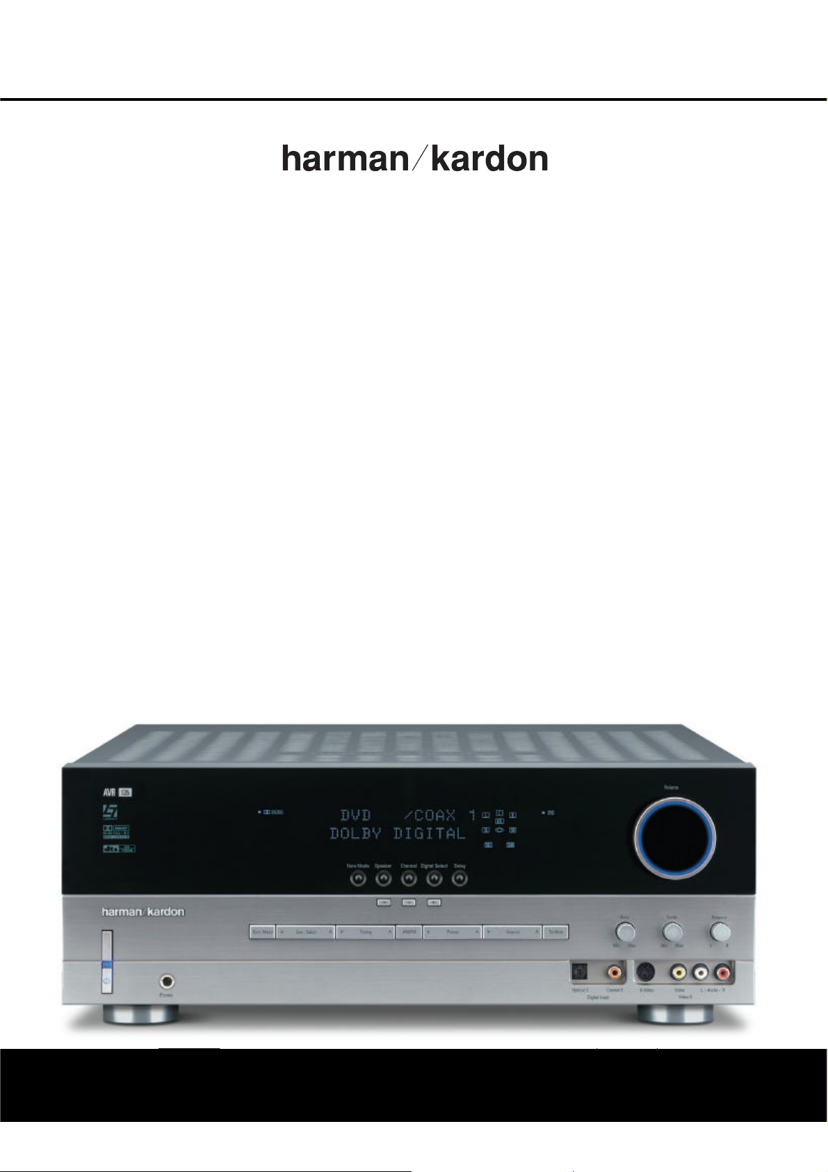
AVR135
AVR135BK
AUDIO/VIDEO RECEIVER
SERVICE MANUAL
230V international version
Page 2

AVR 135 TECHNICAL SPECIFICATIONS
Audio Section
Stereo Mode
Continuous Average Power (FTC)
50 Watts per channel, 20Hz–20kHz,
@ <0.07% THD, both channels driven into 8 ohms
Six-Channel Surround Modes
Power per Individual Channel
Front L&R channels:
40 Watts per channel
@ <0.07% THD, 20Hz–20kHz into 8 ohms
Center channel:
40 Watts @ <0.07% THD, 20Hz–20kHz into 8 ohms
Surround (L & R Side, Back) channels:
40 Watts per channel
@ <0.07% THD, 20Hz–20kHz into 8 ohms
Input Sensitivity/Impedance
Linear (High-Level) 200mV/47k ohms
Signal-to-Noise Ratio (IHF-A) 100dB
Surround System Adjacent Channel Separation
Pro Logic I/II 40dB
Dolby Digital (AC-3) 55dB
DTS 55dB
Frequency Response
@ 1W (+0dB, –3dB) 10Hz –130kHz
High Instantaneous
Current Capability (HCC) ±25 Amps
Transient Intermodulation
Distortion (TIM) Unmeasurable
Slew Rate 40V/μsec
FM Tuner Section
Frequency Range 87.5–108.0MHz
Usable Sensitivity IHF 1.3μV/13.2dBf
Signal-to-Noise Ratio Mono/Stereo 70/68dB
Distortion Mono/Stereo 0.2/0.3%
Stereo Separation 40dB @ 1kHz
Selectivity ±400kHz, 70dB
Image Rejection 80dB
IF Rejection 90dB
AM Tuner Section
Frequency Range 520–1720kHz
Signal-to-Noise Ratio 45dB
Usable Sensitivity Loop 500μV
Distortion 1kHz, 50% Mod 0.8%
Selectivity ±10kHz, 30dB
Video Section
Television Format NTSC
Input Level/Impedance 1Vp-p/75 ohms
Output Level/Impedance 1Vp-p/75 ohms
Video Frequency Response
(Composite and S-Video) 10Hz–8MHz (–3dB)
Video Frequency Response
(Component Video) 10Hz–50MHz (–3dB)
General
Power Requirement AC 120V/60Hz
Power Consumption 65W idle, 540W maximum
(6 channels driven)
Dimensions (Product) (Shipping)
Width 17.3 inches (440mm) 21.5 inches (545mm)
Height 6.6 inches (168mm) 9.9 inches (251mm)
Depth 15 inches (382mm) 17.9 inches (455mm)
(Product) (Shipping)
Weight 24.4 lb (11.1kg) 29.3 lb (13.3kg)
Depth measurement includes knobs, buttons and terminal connections.
Height measurement includes feet and chassis.
All features and specifications are subject to change without notice.
Harman Kardon and Power for the Digital Revolution are registered trademarks of
Harman International Industries, Incorporated.
* Manufactured under license from Dolby Laboratories. “Dolby,” “Pro Logic” and the Double-D symbol
are trademarks of Dolby Laboratories.
DTS, DTS Surround, DTS-ES and DTS Neo:6 are registered trademarks of Digital Theater Systems, Inc.
VMAx is a registered trademark of Harman International Industries, Incorporated, and is an
implementation of Cooper Bauck Transaural Stereo under patent license.
Logic 7 is a registered trademark of Harman International Industries, Incorporated.
Cirrus is a registered trademark of Cirrus Logic, Inc.
46 TECHNICAL SPECIFICATIONS
Page 3
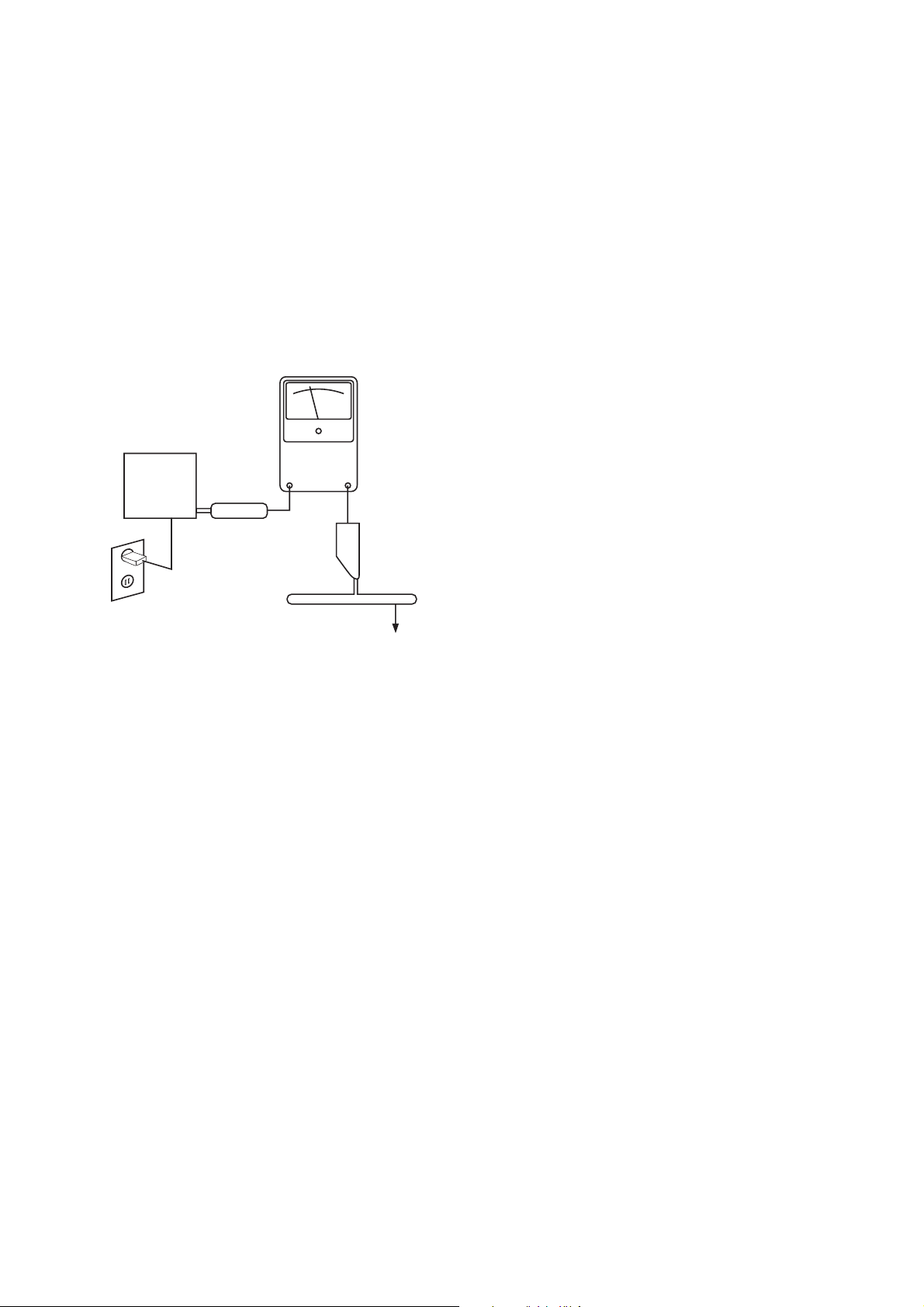
SAFETY PRECAUTIONS
The following check should be performed for the continued
protection of the customer and service technician.
LEAKAGE CURRENT CHECK
Measure leakage current to a known earth ground (water
pipe, conduit, etc.) by connecting a leakage current tester
between the earth ground and all exposed metal parts of the
appliance (input/output terminals, screwheads, metal
overlays, control shaft, etc.). Plug the AC line cord of the
appliance directly into a 250V AC 50Hz outlet and turn the
AC power switch on. Any current measured must not exceed
o.5mA.
Reading should
not be above
0.5mA
Earth
ground
Device
under
test
Test all
exposed metal
surfaces
Also test with
plug reversed
(Using AC adapter
plug as required)
Leakage
current
tester
AC Leakage Test
ANY MEASUREMENTS NOT WITHIN THE LIMITS
OUTLINED ABOVE ARE INDICATIVE OF A
POTENTIAL SHOCK HAZARD AND MUST BE
CORRECTED BEFORE RETURNING THE APPLIANCE
TO THE CUSTOMER.
Page 4

OPERATION
Surround Mode Chart
MODE FEATURES
Dolby Digital Available only with digital input sources encoded with Dolby Digital data. It provides up to five separate main audio channels and
a special dedicated Low-Frequency Effects channel.
Dolby Digital EX Available when the receiver is configured for 6.1/7.1-channel operation, Dolby Digital EX is the latest version of Dolby Digital. When used with
movies or other programs that have special encoding, Dolby Digital EX reproduces specially encoded soundtracks so that a full 6.1/7.1 sound field is
available. When the receiver is set for 6.1/7.1 operation and a Dolby Digital signal is present, the EX mode is automatically selected. Even if specific
EX encoding is not available to provide the additional channel, the special algorithms will derive a 6.1/7.1 output.
DTS 5.1 When the speaker configuration is set for 5.1-channel operation, the DTS 5.1 mode is available when DVD, audio-only music or laser discs encoded
with DTS data are played. DTS 5.1 provides up to five separate main audio channels and a special dedicated low-frequency channel.
DTS-ES 6.1 Matrix When the speaker configuration is set for 6.1/7.1 operation, playback of a DTS-encoded program source will automatically trigger the selection
DTS-ES 6.1 Discrete of one of the two DTS-ES modes. Newer discs with special DTS-ES discrete encoding will be decoded to provide six discrete, full-bandwidth
channels plus a separate low-frequency channel. All other DTS discs will be decoded using the DTS-ES Matrix mode, which creates a 6.1-channel
sound field from the original 5.1-channel soundtrack.
Dolby Pro Logic II Dolby Pro Logic II is the latest version of Dolby Laboratory’s benchmark surround technology that decodes full-range, discrete left, center right,
Movie right surround and left surround channels from either matrix surround-encoded programs and conventional stereo sources when an analog input
Music is in use. The Dolby Pro Logic II Movie mode is optimized for movie soundtracks, while the Pro Logic II Music mode should be used with
Pro Logic musical selections. The Pro Logic mode activates original Pro Logic processing for those who prefer that presentation.
Logic 7 Cinema Exclusive to Harman Kardon for A/V receivers, Logic 7 is an advanced mode that extracts the maximum surround information from either
Logic 7 Music surround-encoded programs or conventional stereo material. Depending on the number of speakers in use and the selection made in the
Logic 7 Enhance
DTS Neo:6 Cinema These two modes are available when any analog source is playing to create a six-channel surround presentation from conventional Matrix-encoded
DTS Neo:6 Music and traditional Stereo sources. Select the Cinema version of Neo:6 when a program with any type of analog Matrix surround encoding is present.
Dolby 3 Stereo Uses the information contained in a surround-encoded or two-channel stereo program to create center-channel information. In addition, the
Theater The Theater mode creates a sound field that resembles the acoustic feeling of a standard live-performance theater.
Hall 1, Hall 2 The two Hall modes create sound fields that resemble a small (Hall 1) and medium-sized (Hall 2) concert hall.
VMAx Near When only the two front-channel loudspeakers are used, Harman’s patented VMAx mode delivers a three-dimensional sound space with the illusion
VMAx Far of “phantom speakers” at the center and surround positions. The VMAx N, or “Near Field,” mode should be selected when your listening position is
5-Channel Stereo This mode takes advantage of multiple speakers to place a stereo signal at both the front and back of a room. Depending on whether the AVR
7-Channel Stereo has been configured for either 5.1 or 6.1/7.1 operation, one of these modes, but not both, is available at any time. Ideal for playing music in
Surround This mode turns off all surround processing and presents the pure left- and right-channel presentation of two-channel stereo programs.
Off (Stereo)
SURROUND SELECT menu, the “5.1” versions of Logic 7 modes are available when the 5.1 option is chosen, while the “7.1” versions of
Logic 7 produce a full sound field presentation, including back surround speakers when the “6.1/7.1” option is chosen. The Logic 7 C (or Cinema)
mode should be used with any source that contains Dolby Surround or similar matrix encoding. Logic 7 C delivers increased center-channel
intelligibility, and more accurate placement of sounds with fades and pans that are much smoother and more realistic than with other decoding
techniques. The Logic 7 M or Music mode should be used with analog or PCM stereo sources. Logic 7 M enhances the listening experience by
presenting a wider front soundstage and greater rear ambience. Both Logic 7 modes also direct low-frequency information to the subwoofer
(if installed and configured) to deliver maximum bass impact. The Logic 7 E (or Enhance) mode, available only when the 5.1 option is chosen,
is an extension of the Logic 7 mode that is primarily used with musical programs. Logic 7 adds additional bass enhancement that circulates low
frequencies in the 40Hz to 120Hz range to the front and surround speakers to deliver a less localized soundstage that appears broader and wider
than when the subwoofer is the sole source of bass energy.
Select the Music version of Neo:6 for optimal processing when a nonencoded, two-channel stereo program is being played.
information that is normally sent to the rear-channel surround speakers is carefully mixed in with the front-left and front-right channels for increased
realism. Use this mode when you have a center channel speaker but no surround speakers.
less than five feet from the speakers. The VMAx F, or “Far Field,” mode should be selected when your listening position is greater than five feet from
the speakers. The VMAx modes are also available using the
appear to push the sound field away from your ears, reducing the “inside the head” sensation often experienced when using headphones.
situations such as a party, it places the same signal at the front-left and surround-left, and front-right and surround-right speakers.
The center channel is fed a summed mono mix of the in-phase material of the left and right channels.
Headphones Output 4. When headphones are being used, the Far Field mode will
24 OPERATION
Page 5

TROUBLESHOOTING GUIDE
SYMPTOM CAUSE SOLUTION
Unit does not function when Main • No AC Power • Make certain AC power cord is plugged into
Power Switch is pushed a live outlet
• Check to see whether outlet is switch-controlled
Display lights, but no sound • Intermittent input connections • Make certain that all input and speaker connections
or picture are secure
•
Mute is on • Press Mute Button
• Volume control is down • Turn up volume control
Unit turns on, but front panel • Display brightness is turned off • Follow the instructions in the Display Brightness section
display does not light up on page 28 so that the display is set to VFD FULL
No sound from any speaker; • Amplifier is in protection mode • Check speaker wire connections for shorts at receiver and
light around power switch is red due to possible short speaker ends
• Amplifier is in protection mode • Contact your local Harman Kardon service center
due to internal problems
No sound from surround or • Incorrect surround mode • Select a mode other than Stereo
center speakers • Input is monaural • There is no surround information from mono sources
• Incorrect configuration • Check speaker mode configuration
• Stereo or Mono program material • The surround decoder may not create center- or rear-channel
information from nonencoded programs
41
Unit does not respond to • Weak batteries in remote • Change remote batteries
remote commands • Wrong device selected • Press the AVR selector
• Remote sensor is obscured • Make certain front panel sensor is visible to remote
or connect remote sensor
Intermittent buzzing in tuner • Local interference • Move unit or antenna away from computers, fluorescent
lights, motors or other electrical appliances
Letters flash in the channel indicator • Digital audio feed paused • Resume play for DVD
display and digital audio stops • Check that Digital Input is selected
In addition to the items shown above, additional information on troubleshooting possible problems with your AVR 135, or installation-related issues, may be found in the list of
"Frequently Asked Questions" which is located in the Product Support section of our Web site at www.harmankardon.com.
Processor Reset
In the rare case where the unit’s operation or the displays seem abnormal, the cause may involve the erratic
operation of the system’s memory or microprocessor.
To correct this problem, first unplug the unit from the
AC wall outlet and wait at least three minutes. After the
pause, reconnect the AC power cord and check the
unit’s operation. If the system still malfunctions, a system reset may clear the problem.
NOTE: Resetting the processor will erase any configuration settings you have made for speakers, output
levels, surround modes, digital input assignments as
well as the tuner presets. The unit will be returned to
the factory presets, and all settings for these items
must be reentered.
If the system is still operating incorrectly, there may
have been an electronic discharge or severe AC line
interference that has corrupted the memory or
microprocessor.
To clear the AVR 135’s entire system memory including tuner presets, output level settings, delay times and
speaker configuration data, press and hold the
Mode Button
will turn on automatically.
5 button for three seconds. The unit
Tone
If these steps do not solve the problem, consult an
authorized Harman Kardon service center.
TROUBLESHOOTING GUIDE 45
Page 6
AMPLIFIER SECTION BIAS ADJUSTMENT
Measurement condition
. No input signal or volume position is minimum.
Standard value.
. Ideal current = 48mA ( ± 5%)
. Ideal DC Voltage = 25.92mV (
± 5%)
CUP11651Y (BIAS PCB)
...... ......
VR87
CN81
VR86
CN82
VR82
CN86
VR81
DC VOLTMETER..............Connect to CN81,CN82,CN83,CN84,CN85,CN86,CN87
NO. Channel Adjust for
1 Front Left 25.92mV (±5%)
2 Front Right 25.92mV (±5%)
3 Center
4 Surround Left
5 Surround Right
6
7
Surround Back Left
Surround Back Right
25.92mV (±5%)
25.92mV (±5%)
25.92mV (±5%)
25.92mV (±5%)
25.92mV (±5%)
Adjustment
VR81(235&335 ONLY)
CN87
VR83
VR84
VR85
VR86
VR87
VR82
Page 7
CHR@RRDLAKX
@UQ024.12/
0-QdlnuhmfsgdSnoB`ahmds
QdlnudsgdRbqdvr
5
3
4
0
2-QdlnuhmfsgdQd`qO`mdk
02
}
0/
8
00
6
7
01
02
2
0
1
QdlnudsgdRbqdvr
7
8
0/
00
01
02
03
6
11
12 14 15
15
0
}
354 2100405
13 16 17
06
18
1/07 08
10
3-QdlnuhmfsgdL`hmOBA
0 7
QdlnudsgdRbqdvr
}
1-QdlnuhmfsgdEqnmsO`mdk
8
7
6
5
4
3
QdlnudsgdRbqdvr
0
1
2
0 8
}
0
4
1
5
2
3
7
6
Page 8
@UQ024.12/DWOKNCDUHDV
24
23
R8
36
3/,3
25
3/,4
R0
26,8
R3
R01
R00
2/
27,1
R02
22
3/,2
3/,0
R7
3/,1
28,0
R5
w1
R4
R3
21
R0/
R4
16
BSA2*0/F
BSVR2*0/F
BSV2*7I
BSA2*7I
BSV2*01I
BSA3*5EEB
BSA2*0/FEY
BGC0@/12
BSA2*5I
BGC0@/01Y
BGC3@/01
BSA2*7IEY
BSA2*05FEY
27,0
30
34
R3
R3
CDRBQHOSHNM
R4
06BSA2*7IEBRBQDV
26
0
8
0/
2
5
18
3
08
1
4
0
1
MN
B@O+UNKTLD
0
GNKCDQ+UNKTLD
1
HMCHB@SNQ+UNKTLD
2
VHMCNV+EHO
3
4
JMNA+QNS@QX
EHKSDQ+EHO
5
AC@FD+G@QL@M.J@QCNM
6
O@MDK+EQNMS
7
AQ@BJDS+RHCD
8
JMNA+ETMBSHNM
0/
JMNA+RDS
00
JMNA+CDK@X
01
JMNA+ONVDQ
02
HMCHB@SNQ+ONVDQ
03
JMNA+LNLR
04
AQ@BJDS+OBA
05
OK@SD+RGHDKC
06
07
GNKCDQ+KDC
08
AQ@BJDS+EHO
1/
B@AHMDS+SNO
10
BG@RRHR+ANSSNL
11
QTAADQ+BTRGHNM
12
ENNS
13
RTOONQS+BTRGHNM
14
GD@SRHMJ
15
AQ@BJDS+OBA
16
GNKCDQ+OBA
17
AQ@BJDS+SQ@MR
18
AQ@BJDS+OBA'G.S(
2/
RGDDS+UNKTLD
20
AQ@BJDS+OBA
21
O@MDK+QD@Q
22
ATRGHMF+@BBNQC
23
BNQC+ONVDQ
24
SQ@MR+ONVDQ
25
EQNMSO@A@RR&X
26
L@HMOBA@RR&X
27
HMOTSOBA@RR&X
28
UHCDNOBA@RR&X
3/
STMDQLNCTKD'DTQ(
30
A@CFD+LNCDK JFA0@035Y 0
31
HMRTK@SNQ+ETMBSHNM BLW0@037 1
32
HMRTK@SNQ+RDS BLW0@038 1
33
BTRGHNM+QTAADQ
34
BTRGHNM
35
A@CFD+SNO BFA0@041Y 0
36
37
38
O@QSRMNBFW0@227LAB11
BLG0@103
BFK0@111
BFT0@206Y
BAM0@063LAB11
BLY0@/77
JFA0@000W
BFV0@255QCYG32
BLC1@332
BAS0@8/4LAXB11
BAS0@8/3LAYB11
BAS0@708J017
BAS0@8/2LLYB11
BFK0@110
BAB0@036LAYB11
BLJ0@/0/
BLB0@1//
BLG0@104
BLC0@1/8
BJB3A034R35
BT@0@118
JGF0@/4/
BJK1@/58G32
BGF0@0/3
BLX0@137
BLC0@306
BGD0@06/
BLC0@376
BLC0@287
BLC0@276
BJE0/@143Y
JGQ0@/17
BI@1A/32Y@
BKS4U/26YD
BNO00634D
EHOOBA
26,0
JDXOBA
26,1
SNMDOBA
26,2
OGNMDOBA
26,3
LNLROBA
26,4
ONVDQKDCOBA
26,5
BNMMDBSNQOBA
26,6
CHFHS@KHMOTSOBA
26,7
CNVMKN@COBA
26,8
BNO00635D
L@HMOBA
27,0
@BNTSKDSROBA
27,1
HMOTSOBA
28,0
BNO00636D
UHCDNOBA
3/,0
CHFHS@KHMOTS.NTSOTSOBA
3/,2
SQ@MROBA
3/,3
SQ@MROBA
3/,4
BMUL8/03LR06/K
BGF0@046 0
BGF0@05/
P+sx
0
0
0
0
2
0
0
0
1
0
0
0
0
0
0
0
0
0
2
0
0
3
3
1
0
1
1
0
1BLC0@287
0
3
0
0
0
0
0
0
0
0
0
0
0
0
0
0
00
0
0
0
0BNO00637D
0
0
0
0
0
0
0
0
1BLW0@06/HMRTK@SNQ+ONVDQ
1BLW0@062HMRTK@SNQ+ETMBSHNM'K(
18
R3
R4
35
R4
11
10
1/
R1
26,4
04
26,5
37
R1
8
03
02
26,3
7
6
5
R1
R1
R2
05
38
R6
26,0
R1
26,7
26,2
R1
R03
17
R0/
15
14
13
12
R3
13
12
R3
08
06
01
33
32
31
8
R0
R0
4
20
3
2
1
07
0
00
0/
R1
CDRBQHOSHNM O@QSRMN- P+sx
MN
R0
RBQDV
R1
RBQDV
R2
RBQDV
R3
RBQDV
R4
RBQDV
R5
RBQDV
R6
RBQDV
R7
RBQDV+SQ@MR
R8
RBQDV
R0/
RBQDV+RODBH@K
R00
RBQDV+RODBH@K
R01
RBQDV
R02
RBQDV
R03
Page 9
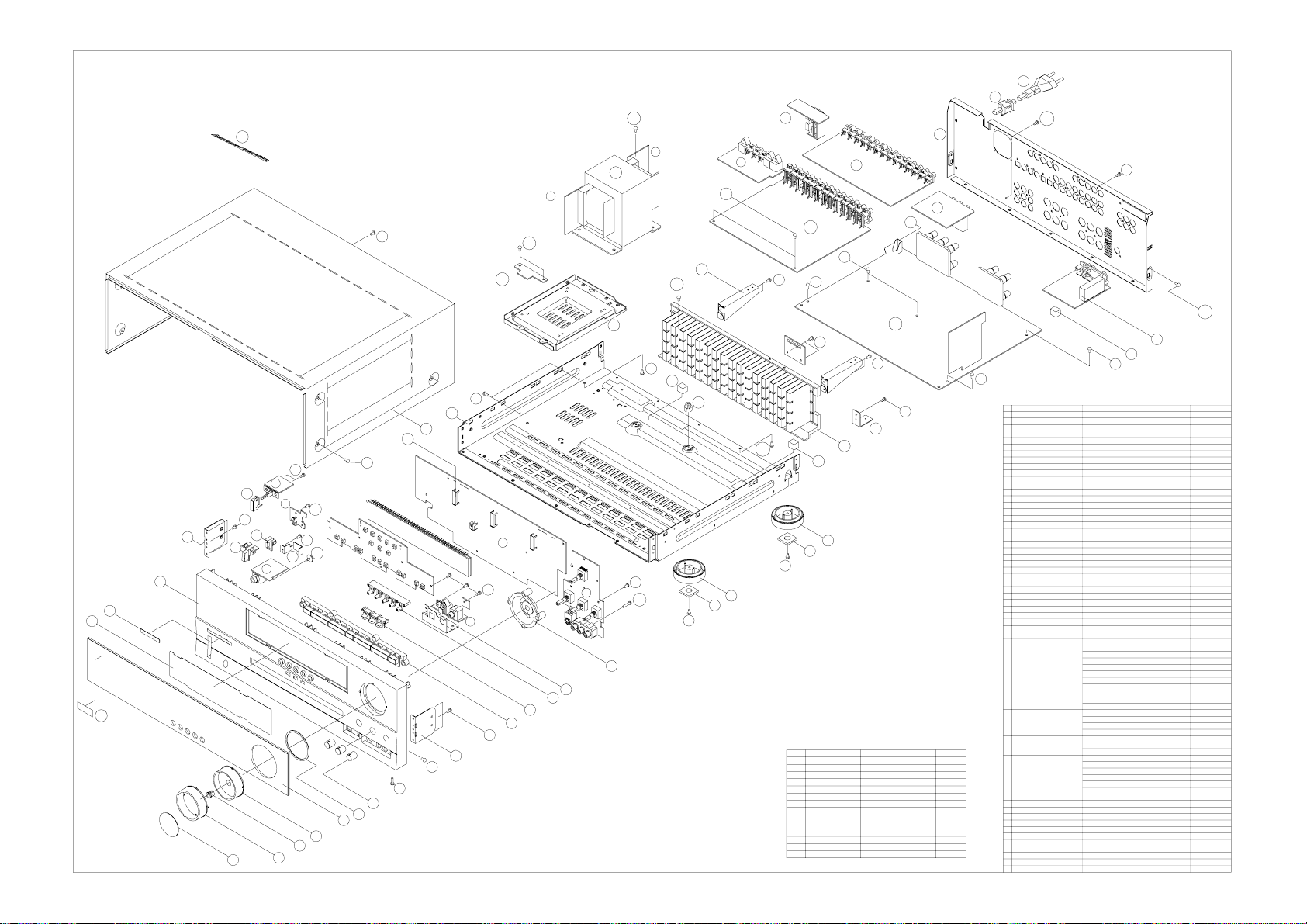
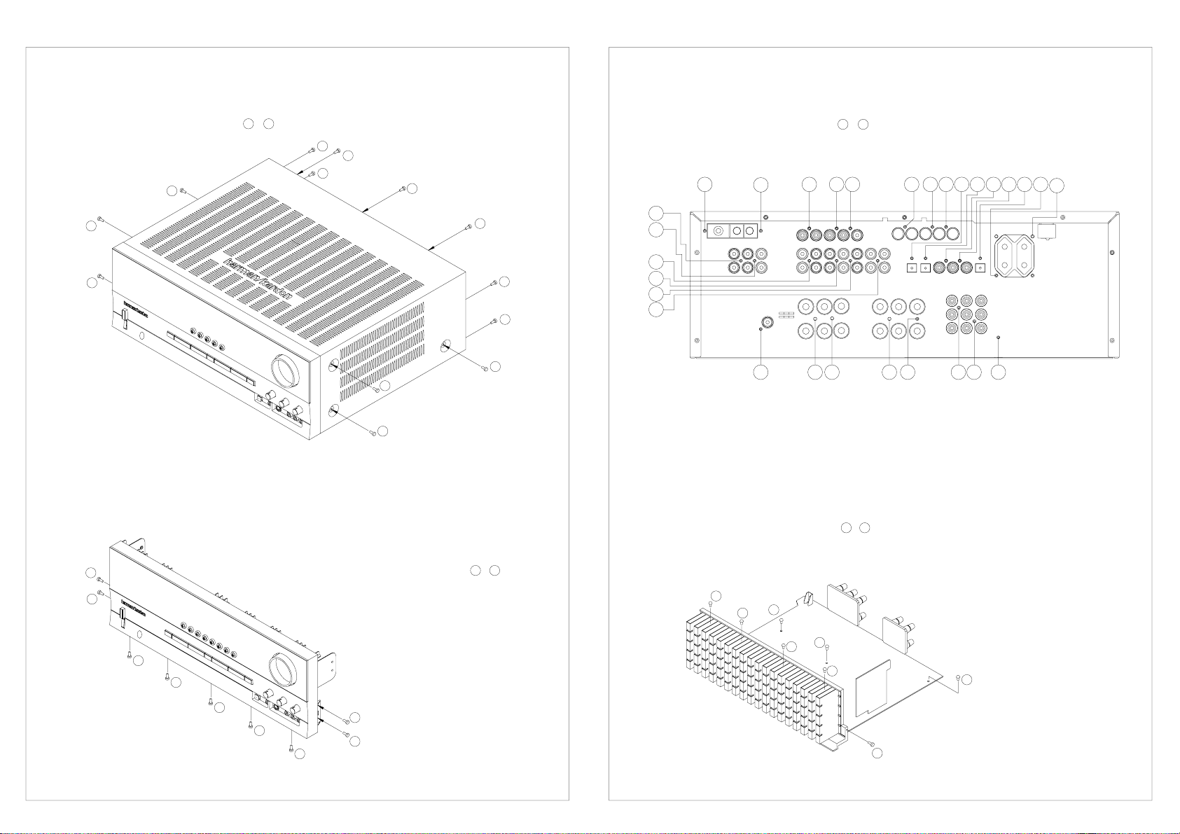
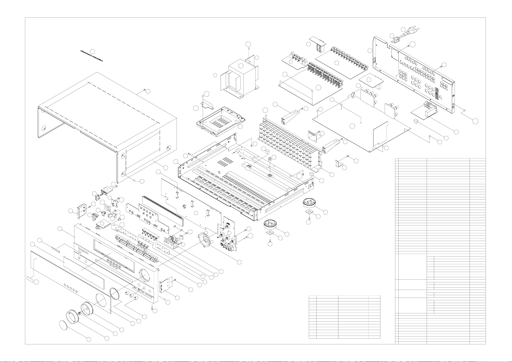
AVR135/230BK EXPLODE VIEW
24
23
R8
36
3/,3
25
3/,4
R0
26,8
R3
R01
R00
2/
27,1
R0
22
3/,2
3/,0
R7
3/,1
28,0
R5
w1
R4
R3
21
R0/
R4
16
BSA2*0/F
BSVR2*0/F
BSV2*7I
BSA2*7I
BSV2*01I
BSA3*5EEY
BSA2*0/FEY
BGC0@/12
BSA2*5I
BGC0@/01Y
BGC3@/01
BSA2*05FEY
27,0
30
34
R3
R3
CDRBQHOSHNM
R4
07BSA2*7IEYRBQDV
26
0
8
0/
2
5
18
3
08
1
4
1
MN
B@O+UNKTLD
0
GNKCDQ+UNKTLD
1
HMCHB@SNQ+UNKTLD
2
VHMCNV+EHO
3
4
JMNA+QNS@QX
EHKSDQ+EHO
5
AC@FD+G@QL@M.J@QCNM
6
O@MDK+EQNMS
7
AQ@BJDS+RHCD
8
JMNA+ETMBSHNM
0/
JMNA+RDS
00
JMNA+CDK@X
01
JMNA+ONVDQ
02
HMCHB@SNQ+ONVDQ
03
JMNA+LNLR
04
AQ@BJDS+OBA
05
OK@SD+RGHDKC
06
07
GNKCDQ+KDC
08
AQ@BJDS+EHO
1/
B@AHMDS+SNO
10
BG@RRHR+ANSSNL
11
QTAADQ+BTRGHNM
12
ENNS
13
RTOONQS+BTRGHNM
14
GD@SRHMJ
15
AQ@BJDS+OBA
16
GNKCDQ+OBA
17
AQ@BJDS+SQ@MR
18
AQ@BJDS+OBA'G.S(
2/
RGDDS+UNKTLD
20
AQ@BJDS+OBA
21
O@MDK+QD@Q
22
ATRGHMF+@BBNQC
23
BNQC+ONVDQ
24
SQ@MR+ONVDQ
25
EQNMSO@A@RR&X
26
L@HMOBA@RR&X
27
HMOTSOBA@RR&X
28
UHCDNOBA@RR&X
3/
STMDQLNCTKD'DTQ(
30
A@CFD+LNCDK JFA0@035Y 0
31
BTRGHNM+QTAADQ
34
BTRGHNM
35
A@CFD+SNO BFA0@041Y 0
36
O@QSRMNBFW0@227LAF16
BLG0@103
BFK0@111
BFT0@206Y
BAM0@063A2
BLY0@/77
JFA0@000W
BFV0@255Q3YG0/
BLC1@332
BAS0@8/4LAXF16
BAS0@8/3LAYF16
BAS0@708J017
BAS0@8/2LLXF16
BFK0@110
BAB0@036LAYF16
BLJ0@/0/
BLB0@1//
BLG0@104
BLC0@1/8
BJB3A034R0Y
BT@0@118
JGF0@/4/
BJK1@/58G32
BGF0@0/3
BLX0@137
BLC0@306
BGD0@06/
BLC0@376
BLC0@287
BLC0@276
BJE0/@143Y
JGQ0@/17
BI@1A/32Y@
BKS4U/26YD
BNO00634D
EHOOBA
26,0
JDXOBA
26,1
SNMDOBA
26,2
OGNMDOBA
26,3
LNLROBA
26,4
ONVDQKDCOBA
26,5
BNMMDBSNQOBA
26,6
CHFHS@KHMOTSOBA
26,7
CNVMKN@COBA
26,8
BNO00635D
L@HMOBA
27,0
@BNTSKDSROBA
27,1
HMOTSOBA
28,0
BNO00636D
UHCDNOBA
3/,0
CHFHS@KHMOTS.NTSOTSOBA
3/,2
SQ@MROBA
3/,3
SQ@MROBA
3/,4
BMUL8/03LR06/K
BGF0@046 0
BGF0@05/
P+sx
0
0
0
0
2
0
0
0
1
0
0
0
0
0
0
0
0
0
2
0
0
3
3
1
0
1
1
0
1BLC0@287
0
3
0
0
0
0
0
0
0
0
0
0
0
0
0
0
00
0
0
0
0BNO00637D
0
0
0
0
0
0
0
0
18
R3
R4
35
R4
11
10
1/
R1
26,4
04
26,5
R1
8
03
02
26,3
R1
R1
R2
05
7
6
5
R6
26,0
R1
26,7
26,2
R1
R03
17
R0/
15
14
13
12
R3
13
12
R3
08
06
01
31
8
R0
R0
4
20
3
2
1
07
0
00
0/
R1
CDRBQHOSHNM O@QSRMN- P+sx
MN
R0
RBQDV
R1
RBQDV
R2
RBQDV
R3
RBQDV
R4
RBQDV
R5
RBQDV
R6
RBQDV
R7
RBQDV+SQ@MR
R8
RBQDV
R0/
RBQDV+RODBH@K
R00
RBQDV+RODBH@K
R01
R02
RBQDV
R03
Page 10
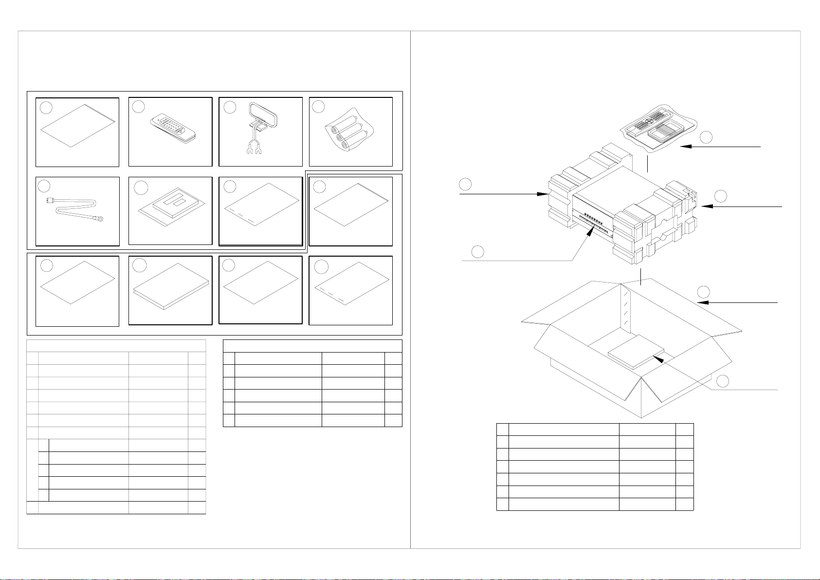
0-Hmrsqtbshnml`mt`k`rr&x,@bbdrrnqhdr 1-O`bj`fdCq`vhmf
BLACK
@UQ024.12/
0
ONKXA@F
4
EL0ONKD@MS
8
ANNJKDS+HMENQL@SHNM
MN CDRBQHOSHNM O@QSRMN- P+sx
0
1
QDLNBNMSQ@MRLHSSDQ@RR&X
2
3
EL0ONK@MS'TK( BR@0@/07Y 0
4
5
BNUDQ@RR&X
BNUDQ@
0
BNUDQA
1
RGDDS+EQNMSBNUDQ
2
O@C+BNUDQ
3
4
A@F+ONKX
6
RS@OKD JOK/8/4 2
1
QDLNBNM
SQ@MRLHSSDQ@RR&X
5
BNUDQ@RR&X
0/
L@MT@KHMRSQTBSHNM
BOA0/50XONKXA@F
HARTAVR135/230B
BR@0@/16Y@LKNNO@MSDMM@@RR&X 0
G@A@@@L0-4UGJA@SSDQX 2
CGRAVR130/230BZA
CGR1A331H10 1
CGR1A331H10 1
BPD0@11/Y
BOR0@565 0
BOA0@065Y 0
2
@LKNNO@MSDMM@@RR&X
6
RS@OKD
00
L@MT@KRDSTOFTHCD
3
7
01
RS@OKD
@BBDRRNQX,1@BBDRRNQX,0
MN CDRBQHOSHNM O@QSRMN- P+sx
0
0
0
0
0
7
ANNJKDS+HMENQL@SHNM
8
0/
00
L@MT@K+RDSTOFTHCD
01
RS@OKD JOK/8/4 2
BPD0@07/Y 0
BPW0@841YL@MT@K+HMRSQTBSHNM
BPW0@0/02Y
A@SSDQX@RR&X
ONKXA@F
@BBDRRNQX,0
0
1
RMNVO@C'K(
RDS
3
0BOA0/50XONKXA@F
0
0
CDRBQHOSHNMMN
@BBDRRNQX,0
0
1
RMNV+O@C'K(
RMNV+O@C'Q(20
RDS
3
ANW+NTSB@QSNM
4
61
@BBDRRNQX,1
CQXAVR135/230BK
BOR3@453
BOR3@454
AVR135/230BKSET
CPG1A775M
CQXAVR135/230BK
P+sxO@QSRMN-
0
0
0
0
RMNVO@C'Q(
2
ANW+NTSB@QSNM
4
@BBDRRNQX,1
5
Page 11

0-Hmrsqtbshnml`mt`k`rr&x,@bbdrrnqhdr 1-O`bj`fdCq`vhmf
@UQ024.12/
0
ONKXA@F
4
EL0ONKD@MS
8
ANNJKDS+HMENQL@SHNM
MN CDRBQHOSHNM O@QSRMN- P+sx
0
1
QDLNBNMSQ@MRLHSSDQ@RR&X
2
3
EL0ONK@MS'TK( BR@0@/07Y 0
4
5
BNUDQ@RR&X BFQ@UQ02/.12/Y@
BNUDQ@
0
BNUDQA
1
RGDDS+EQNMSBNUDQ
2
O@C+BNUDQ
3
4
A@F+ONKX
6
RS@OKD JOK/8/4 2
1
QDLNBNM
SQ@MRLHSSDQ@RR&X
5
BNUDQ@RR&X
0/
L@MT@KHMRSQTBSHNM
BOA0/50XONKXA@F
G@QS@UQ024.12/
BR@0@/16Y@LKNNO@MSDMM@@RR&X 0
G@A@@@L0-4UGJA@SSDQX 2
BFQ0@220L6G32 0
BPD0@11/Y
BOR0@565 0
BOA0@065Y 0
2
@LKNNO@MSDMM@@RR&X
6
RS@OKD
00
L@MT@KRDSTOFTHCD
3
7
01
RS@OKD
@BBDRRNQX,1@BBDRRNQX,0
MN CDRBQHOSHNM O@QSRMN- P+sx
0
0
0
0
0BFQ0@221L6G32
0
7
ANNJKDS+HMENQL@SHNM
8
0/
00
L@MT@K+RDSTOFTHCD
01
RS@OKD JOK/8/4 2
BPD0@07/Y 0
BPW0@841YL@MT@K+HMRSQTBSHNM
BPW0@0/02Y
A@SSDQX@RR&X
ONKXA@F
@BBDRRNQX,0
0
1
RMNVO@C'K(
RDS
3
0BOA0/50XONKXA@F
0
0
CDRBQHOSHNMMN
@BBDRRNQX,0
0
1
RMNV+O@C'K(
RMNV+O@C'Q(20
RDS
3
ANW+NTSB@QSNM
4
50
@BBDRRNQX,1 BPW@UQ024.12/
BPW@UQ024.12/
BOR3@453
BOR3@454
@UQ024.12/RDS
BOF0@664V
P+sxO@QSRMN-
0
0
0
0
RMNVO@C'Q(
2
ANW+NTSB@QSNM
4
@BBDRRNQX,1
5
Page 12

AVR135/230SET
Ref# Component Description 1 Description 2 Qty
CNVM9014MS170L TUNER MODULE(EUR) 1
T901 CLT5V037ZE TRANS , POWER 1
AV SURROUND RECEIVER
FRONT PCB
Ref# Component Description 1 Description 2 Qty
COP11745E FRONT PCB ASS'Y 1
C701 HCBS1H390JT CAP , CERAMIC 39PF 50V J 1
C702 HCBS1H390JT CAP , CERAMIC 39PF 50V J 1
C703 HCBS1H821KBT CAP , CERAMIC 820PF 50V K 1
C704 HCEA1VH100T CAP , ELECT 10UF 35V 1
C705 HCBS1H102KBT CAP , CERAMIC 1000PF 50V B 1
C706 HCBS1H561KBT CAP , CERAMIC 560PF 50V 1
C708 HCBS1H223ZFT CAP , CERAMIC 0.022UF 50V Z 1
C709 CCEA1CH101T CAP , ELECT 100UF 16V 1
C710 CCEA1HH2R2T CAP , ELECT 2.2UF 50V 1
C711 HCBS1H102KBT CAP , CERAMIC 1000PF 50V B 1
C712 HCEA1HH1R0T CAP , ELECT 1UF 50V 1
C713 HCBS1H223ZFT CAP , CERAMIC 0.022UF 50V Z 1
C714 HCBS1H151KBT CAP , CERAMIC 150PF 50V K 1
C716 HCEA1CH331T CAP , ELECT 330UF 16V 1
C719 HCBS1H181KBT CAP , CERAMIC 180PF 50V K 1
C720 HCBS1H181KBT CAP , CERAMIC 180PF 50V K 1
C721 HCBS1H181KBT CAP , CERAMIC 180PF 50V K 1
C723 HCBS1H104ZFT CAP , CERAMIC 0.1UF 50V Z 1
C724 HCBS1H223ZFT CAP , CERAMIC 0.022UF 50V Z 1
C725 CCKT1H473ZF CAP , CERAMIC 0.047UF 50V ZF 1
C726 HCEA1CH101T CAP , ELECT 100UF 16V 1
C728 HCBS1H104ZFT CAP , CERAMIC 0.1UF 50V Z 1
C729 CCKT1H473ZF CAP , CERAMIC 0.047UF 50V ZF 1
C730 HCBS1H104ZFT CAP , CERAMIC 0.1UF 50V Z 1
C731 HCEA1HH100T CAP , ELECT 10UF 50V 1
C735 CCEA1CH101T CAP , ELECT 100UF 16V 1
C736 HCBS1H223ZFT CAP , CERAMIC 0.022UF 50V Z 1
C737 HCBS1H180JCT CAP , CERAMIC 18PF 50V 1
C738 HCBS1H180JCT CAP , CERAMIC 18PF 50V 1
C739 CCEA1AH221T CAP , ELECT 220UF/10V 1
C740 CCEA1VH100T CAP , ELECT 10UF 35V 1
C770 HCBS1H223ZFT CAP , CERAMIC 0.022UF 50V Z 1
C771 HCBS1H223ZFT CAP , CERAMIC 0.022UF 50V Z 1
C773 HCEA1VH100T CAP , ELECT 10UF 35V 1
C774 HCEA1VH100T CAP , ELECT 10UF 35V 1
C775 HCBS1H151KBT CAP , CERAMIC 150PF 50V K 1
C776 HCBS1H151KBT CAP , CERAMIC 150PF 50V K 1
C777 HCEA1VH100T CAP , ELECT 10UF 35V 1
C778 HCEA1VH100T CAP , ELECT 10UF 35V 1
C779 HCEA1CKS470T CAP , ELECT 47UF 16V 1
C780 HCEA1CKS470T CAP , ELECT 47UF 16V 1
C781 HCEA1CKS100T CAP , ELECT 10UF 16V 1
C782 HCEA1CKS100T CAP , ELECT 10UF 16V 1
C785 HCBS1H470JT CAP , CERAMIC 47PF 50V J 1
C786 HCBS1H470JT CAP , CERAMIC 47PF 50V J 1
C787 HCEA1CKS100T CAP , ELECT 10UF 16V 1
C788 HCEA1CKS100T CAP , ELECT 10UF 16V 1
C789 HCEA1CKS100T CAP , ELECT 10UF 16V 1
C790 HCEA1CKS100T CAP , ELECT 10UF 16V 1
C791 HCEA1CKS470T CAP , ELECT 47UF 16V 1
C792 HCEA1CKS470T CAP , ELECT 47UF 16V 1
C793 KCFE1J183JBT CAP , FILM 0.018UF 63V J 1
+DUPDQ&RQVXPHU*URXS,QWHUQDO %LOORI0DWHULDOV $95
Page 13

FRONT PCB
Ref# Component Description 1 Description 2 Qty
C794 KCFE1J183JBT CAP , FILM 0.018UF 63V J 1
C795 KCFE1J823JBT CAP , FILM 0.082UF 63V J 1
C796 KCFE1J823JBT CAP , FILM 0.082UF 63V J 1
C797 KCFE1J332JBT CAP , FILM 0.0033UF 63V J 1
C798 KCFE1J332JBT CAP , FILM 0.0033UF 63V J 1
C799 KCFE1J183JBT CAP , FILM 0.018UF 63V J 1
C800 KCFE1J183JBT CAP , FILM 0.018UF 63V J 1
C805 HCBS1H223ZFT CAP , CERAMIC 0.022UF 50V Z 1
C806 HCBS1H223ZFT CAP , CERAMIC 0.022UF 50V Z 1
C807 CCFT1H104ZF CAP , SEMICONDUCTOR 0.1UF 50V ZF 1
C808 CCKT1H181KB CAP , CERAMIC 180PF 50V KB 1
C809 HCEA1AH471T CAP , ELECT 470UF 10V 1
C810 HCEA1CH101T CAP , ELECT 100UF 16V 1
C811 HCEA1CH101T CAP , ELECT 100UF 16V 1
C813 HCEA1HH4R7T CAP , ELECT 4.7UF 50V 1
C814 HCEA1HH4R7T CAP , ELECT 4.7UF 50V 1
C850 HCBS1H471KBT CAP , CERAMIC 470PF 50V 1
C851 HCBS1H471KBT CAP , CERAMIC 470PF 50V 1
C852 HCBS1H104ZFT CAP , CERAMIC 0.1UF 50V Z 1
C855 HCBS1H101KBT CAP , CERAMIC 100PF 50V K 1
C856 HCBS1H101KBT CAP , CERAMIC 100PF 50V K 1
C857 HCBS1H104ZFT CAP , CERAMIC 0.1UF 50V Z 1
C859 HCBS1H223ZFT CAP , CERAMIC 0.022UF 50V Z 1
C860 HCBS1H223ZFT CAP , CERAMIC 0.022UF 50V Z 1
C861 HCBS1H223ZFT CAP , CERAMIC 0.022UF 50V Z 1
C862 HCBS1H101KBT CAP , CERAMIC 100PF 50V K 1
C863 HCBS1H101KBT CAP , CERAMIC 100PF 50V K 1
C866 HCEA1CKS100T CAP , ELECT 10UF 16V 1
C867 HCEA1CKS100T CAP , ELECT 10UF 16V 1
C868 HCEA1CKS470T CAP , ELECT 47UF 16V 1
C869 HCEA1CKS470T CAP , ELECT 47UF 16V 1
C870 HCBS1H681KBT CAP , CERAMIC 680PF 50V 1
C871 HCBS1H681KBT CAP , CERAMIC 680PF 50V 1
C872 HCEA1CH331T CAP , ELECT 330UF 16V 1
C873 HCEA1CH331T CAP , ELECT 330UF 16V 1
C874 HCBS1H101KBT CAP , CERAMIC 100PF 50V K 1
C875 HCBS1H473ZFT CAP , CERAMIC 0.047UF 50V Z 1
C876 HCBS1H473ZFT CAP , CERAMIC 0.047UF 50V Z 1
C877 HCBS1H473ZFT CAP , CERAMIC 0.047UF 50V Z 1
C878 HCBS1H473ZFT CAP , CERAMIC 0.047UF 50V Z 1
C882 HCBS1H104ZFT CAP , CERAMIC 0.1UF 50V Z 1
C886 CCEA0JH102T CAP , ELECT 1000UF 6.3V 1
C887 HCBS1H101KBT CAP , CERAMIC 100PF 50V K 1
C888 HCBS1H101KBT CAP , CERAMIC 100PF 50V K 1
C889 HCBS1H220JCT CAP , CERAMIC 22PF 50V J 1
C890 HCBS1H220JCT CAP , CERAMIC 22PF 50V J 1
C891 HCBS1H223ZFT CAP , CERAMIC 0.022UF 50V Z 1
C892 HCBS1H223ZFT CAP , CERAMIC 0.022UF 50V Z 1
C893 HCBS1H223ZFT CAP , CERAMIC 0.022UF 50V Z 1
C894 HCBS1H223ZFT CAP , CERAMIC 0.022UF 50V Z 1
C895 HCEA1AH471T CAP , ELECT 470UF 10V 1
C896 HCBS1H223ZFT CAP , CERAMIC 0.022UF 50V Z 1
C897 HCEA1AH471T CAP , ELECT 470UF 10V 1
C898 HCBS1H223ZFT CAP , CERAMIC 0.022UF 50V Z 1
C899 HCBS1H223ZFT CAP , CERAMIC 0.022UF 50V Z 1
C900 HCBS1H104ZFT CAP , CERAMIC 0.1UF 50V Z 1
C901 HCBS1H104ZFT CAP , CERAMIC 0.1UF 50V Z 1
+DUPDQ&RQVXPHU*URXS,QWHUQDO %LOORI0DWHULDOV $95
Page 14

FRONT PCB
Ref# Component Description 1 Description 2 Qty
C903 HCEA1HH2R2T CAP , ELECT 2.2UF 50V 1
C905 HCEA1HH2R2T CAP , ELECT 2.2UF 50V 1
D724 HVD1SS133MT DIODE 1SS133T-77 1
D728 HVD1SS133MT DIODE 1SS133T-77 1
D729 HVD1SS133MT DIODE 1SS133T-77 1
D730 HVD1SS133MT DIODE 1SS133T-77 1
D774 HVD1SS133MT DIODE 1SS133T-77 1
D778 KVD1N4003ST DIODE 1N4003 1
D779 HVD1SS133MT DIODE 1SS133T-77 1
D780 HVD1SS133MT DIODE 1SS133T-77 1
D781 HVD1SS133MT DIODE 1SS133T-77 1
D782 KVD1N4003ST DIODE 1N4003 1
D783 HVD1SS133MT DIODE 1SS133T-77 1
D784 HVD1SS133MT DIODE 1SS133T-77 1
D785 HVD1SS133MT DIODE 1SS133T-77 1
D786 HVDMTZJ5.6BT DIODE , ZENER 5.6V 1
D787 HVDMTZJ5.6BT DIODE , ZENER 5.6V 1
IC87 HVIRE5VL28CATZ IC , RESET RE5VL28CATZ 1
L702 HLQ02C100KT COIL , AXAIL 10UH 1
Q701 HVTKRC107MT T.R KRC107M 1
Q702 HVTKRC107MT T.R KRC107M 1
Q703 HVTKRC107MT T.R KRC107M 1
Q705 HVTKRC107MT T.R KRC107M 1
Q706 HVTKRC107MT T.R KRC107M 1
Q722 HVTKRA107MT T.R KRA107M 1
Q724 HVTKRC107MT T.R KRC107M 1
Q725 HVTKRC107MT T.R KRC107M 1
Q726 HVTKRC107MT T.R KRC107M 1
Q727 HVTKRC107MT T.R KRC107M 1
Q728 HVTKRC107MT T.R KRC107M 1
Q729 HVTKRC107MT T.R KRC107M 1
Q734 HVTKTC2874BT T.R , MUTE KTC2874B 1
Q735 HVTKTC2874BT T.R , MUTE KTC2874B 1
Q736 HVTKTC2874BT T.R , MUTE KTC2874B 1
Q737 HVTKTC2874BT T.R , MUTE KTC2874B 1
Q738 HVTKRC107MT T.R KRC107M 1
Q739 HVTKTA1271YT T.R KTA1271Y 1
Q743 HVTKRA107MT T.R KRA107M 1
R701 CRD20TJ103T RES , CARBON 10K OHM 1/5W J 1
R702 CRD20TJ1R0T RES , CARBON 1 OHM 1/5W J 1
R703 CRD20TJ103T RES , CARBON 10K OHM 1/5W J 1
R704 CRD20TJ100T RES , CARBON 10 OHM 1/5W J 1
R705 CRD20TJ820T RES , CARBON 82 OHM 1/5W J 1
R706 CRD20TJ820T RES , CARBON 82 OHM 1/5W J 1
R707 CRD20TJ820T RES , CARBON 82 OHM 1/5W J 1
R708 CRD20TJ820T RES , CARBON 82 OHM 1/5W J 1
R709 CRD20TJ470T RES , CARBON 47 OHM 1/5W J 1
R710 CRD20TJ470T RES , CARBON 47 OHM 1/5W J 1
R711 CRD20TJ470T RES , CARBON 47 OHM 1/5W J 1
R712 CRD20TJ470T RES , CARBON 47 OHM 1/5W J 1
R713 CRD20TJ332T RES , CARBON 3.3K OHM 1/5W J 1
R716 CRD20TJ102T RES , CARBON 1K OHM 1/5W J 1
R717 CRD20TJ103T RES , CARBON 10K OHM 1/5W J 1
R718 CRD20TJ222T RES , CARBON 2.2K OHM 1/5W J 1
R719 CRD20TJ102T RES , CARBON 1K OHM 1/5W J 1
R721 CRD20TJ103T RES , CARBON 10K OHM 1/5W J 1
R722 CRD20TJ1R0T RES , CARBON 1 OHM 1/5W J 1
+DUPDQ&RQVXPHU*URXS,QWHUQDO %LOORI0DWHULDOV $95
Page 15

FRONT PCB
Ref# Component Description 1 Description 2 Qty
R723 CRD20TJ222T RES , CARBON 2.2K OHM 1/5W J 1
R724 CRD20TJ102T RES , CARBON 1K OHM 1/5W J 1
R725 CRD20TJ103T RES , CARBON 10K OHM 1/5W J 1
R726 CRD20TJ103T RES , CARBON 10K OHM 1/5W J 1
R727 CRD20TJ102T RES , CARBON 1K OHM 1/5W J 1
R728 CRD20TJ101T RES , CARBON 100 OHM 1/5W J 1
R730 CRD20TJ112T RES,CABON 1.1K OHM 1/5W J 1
R731 CRD20TJ223T RES , CARBON 22K OHM 1/5W J 1
R732 CRD20TJ202T RES , CARBON 22K OHM 1/5W J 1
R733 CRD20TJ272T RES , CARBON 2.7K OHM 1/5W J 1
R734 CRD20TJ103T RES , CARBON 10K OHM 1/5W J 1
R735 CRD20TJ103T RES , CARBON 10K OHM 1/5W J 1
R736 CRD20TJ272T RES , CARBON 2.7K OHM 1/5W J 1
R737 CRD20TJ100T RES , CARBON 10 OHM 1/5W J 1
R744 CRD20TJ103T RES , CARBON 10K OHM 1/5W J 1
R745 CRD20TJ103T RES , CARBON 10K OHM 1/5W J 1
R746 CRD20TJ103T RES , CARBON 10K OHM 1/5W J 1
R747 CRD20TJ103T RES , CARBON 10K OHM 1/5W J 1
R749 CRD20TJ223T RES , CARBON 22K OHM 1/5W J 1
R750 CRD20TJ223T RES , CARBON 22K OHM 1/5W J 1
R751 CRD20TJ223T RES , CARBON 22K OHM 1/5W J 1
R753 CRD20TJ102T RES , CARBON 1K OHM 1/5W J 1
R754 CRD20TJ152T RES , CARBON 1.5K OHM 1/5W J 1
R755 CRD20TJ182T RES , CARBON 1.8K OHM 1/5W J 1
R756 CRD20TJ272T RES , CARBON 2.7K OHM 1/5W J 1
R757 CRD20TJ332T RES , CARBON 3.3K OHM 1/5W J 1
R758 CRD20TJ562T RES , CARBON 5.6K OHM 1/5W J 1
R759 CRD20TJ102T RES , CARBON 1K OHM 1/5W J 1
R760 CRD20TJ152T RES , CARBON 1.5K OHM 1/5W J 1
R761 CRD20TJ182T RES , CARBON 1.8K OHM 1/5W J 1
R762 CRD20TJ272T RES , CARBON 2.7K OHM 1/5W J 1
R763 CRD20TJ332T RES , CARBON 3.3K OHM 1/5W J 1
R764 CRD20TJ562T RES , CARBON 5.6K OHM 1/5W J 1
R765 CRD20TJ752T RES , CARBON 7.5K OHM 1/5W J 1
R766 CRD20TJ102T RES , CARBON 1K OHM 1/5W J 1
R767 CRD20TJ152T RES , CARBON 1.5K OHM 1/5W J 1
R768 CRD20TJ182T RES , CARBON 1.8K OHM 1/5W J 1
R769 CRD20TJ272T RES , CARBON 2.7K OHM 1/5W J 1
R771 CRD20TJ103T RES , CARBON 10K OHM 1/5W J 1
R772 CRD20TJ103T RES , CARBON 10K OHM 1/5W J 1
R773 CRD20TJ103T RES , CARBON 10K OHM 1/5W J 1
R780 CRD20TJ100T RES , CARBON 10 OHM 1/5W J 1
R781 CRD20TJ123T RES , CARBON 12K OHM 1/5W J 1
R805 CRD20TJ104T RES , CARBON 100K OHM 1/5W J 1
R806 CRD20TJ472T RES , CARBON 4.7K OHM 1/5W J 1
R810 CRD20TJ101T RES , CARBON 100 OHM 1/5W J 1
R811 CRD20TJ101T RES , CARBON 100 OHM 1/5W J 1
R813 CRD20TJ104T RES , CARBON 100K OHM 1/5W J 1
R814 CRD20TJ104T RES , CARBON 100K OHM 1/5W J 1
R824 CRD20TJ221T RES , CARBON 220 OHM 1/5W J 1
R825 CRD20TJ681T RES , CARBON 680 OHM 1/5W J 1
R826 CRD20TJ102T RES , CARBON 1K OHM 1/5W J 1
R827 CRD20TJ102T RES , CARBON 1K OHM 1/5W J 1
R829 CRD20TJ184T RES , CARBON 180K OHM 1/5W 1
R830 CRD20TJ184T RES , CARBON 180K OHM 1/5W 1
R831 CRD20TJ562T RES , CARBON 5.6K OHM 1/5W J 1
R832 CRD20TJ562T RES , CARBON 5.6K OHM 1/5W J 1
+DUPDQ&RQVXPHU*URXS,QWHUQDO %LOORI0DWHULDOV $95
Page 16

FRONT PCB
Ref# Component Description 1 Description 2 Qty
R833 CRD20TJ102T RES , CARBON 1K OHM 1/5W J 1
R834 CRD20TJ102T RES , CARBON 1K OHM 1/5W J 1
R835 CRD20TJ184T RES , CARBON 180K OHM 1/5W 1
R836 CRD20TJ184T RES , CARBON 180K OHM 1/5W 1
R837 CRD20TJ101T RES , CARBON 100 OHM 1/5W J 1
R838 CRD20TJ101T RES , CARBON 100 OHM 1/5W J 1
R839 CRD20TJ104T RES , CARBON 100K OHM 1/5W J 1
R840 CRD20TJ104T RES , CARBON 100K OHM 1/5W J 1
R841 CRD20TJ473T RES , CARBON 47K OHM 1/5W J 1
R842 CRD20TJ473T RES , CARBON 47K OHM 1/5W J 1
R843 CRD20TJ105T RES , CARBON 1M OHM 1/5W J 1
R844 CRD20TJ105T RES , CARBON 1M OHM 1/5W J 1
R845 CRD20TJ104T RES , CARBON 100K OHM 1/5W J 1
R846 CRD20TJ104T RES , CARBON 100K OHM 1/5W J 1
R847 CRD20TJ102T RES , CARBON 1K OHM 1/5W J 1
R848 CRD20TJ102T RES , CARBON 1K OHM 1/5W J 1
R849 CRD20TJ223T RES , CARBON 22K OHM 1/5W J 1
R850 CRD20TJ223T RES , CARBON 22K OHM 1/5W J 1
R851 CRD20TJ392T RES , CARBON 3.9K OHM 1/5W J 1
R852 CRD20TJ392T RES , CARBON 3.9K OHM 1/5W J 1
R853 CRD20TJ222T RES , CARBON 2.2K OHM 1/5W J 1
R854 CRD20TJ222T RES , CARBON 2.2K OHM 1/5W J 1
R855 CRD20TJ681T RES , CARBON 680 OHM 1/5W J 1
R856 CRD20TJ681T RES , CARBON 680 OHM 1/5W J 1
R857 CRD20TJ221T RES , CARBON 220 OHM 1/5W J 1
R858 CRD20TJ221T RES , CARBON 220 OHM 1/5W J 1
R864 CRD20TJ272T RES , CARBON 2.7K OHM 1/5W J 1
R865 CRD20TJ101T RES , CARBON 100 OHM 1/5W J 1
R866 CRD20TJ272T RES , CARBON 2.7K OHM 1/5W J 1
R869 CRD20TJ750T RES , CARBON 75 OHM 1/5W J 1
R871 CRD20TJ104T RES , CARBON 100K OHM 1/5W J 1
R872 CRD20TJ104T RES , CARBON 100K OHM 1/5W J 1
R873 CRD20TJ471T RES , CARBON 470 OHM 1/5W J 1
R874 CRD20TJ471T RES , CARBON 470 OHM 1/5W J 1
R875 CRD20TJ103T RES , CARBON 10K OHM 1/5W J 1
R876 CRD20TJ750T RES , CARBON 75 OHM 1/5W J 1
R877 CRD20TJ750T RES , CARBON 75 OHM 1/5W J 1
R878 CRD20TJ750T RES , CARBON 75 OHM 1/5W J 1
R881 CRD20TJ103T RES , CARBON 10K OHM 1/5W J 1
R882 CRD20TJ103T RES , CARBON 10K OHM 1/5W J 1
R883 CRD20TJ103T RES , CARBON 10K OHM 1/5W J 1
R884 CRD20TJ103T RES , CARBON 10K OHM 1/5W J 1
R885 CRD20TJ103T RES , CARBON 10K OHM 1/5W J 1
R886 CRD20TJ103T RES , CARBON 10K OHM 1/5W J 1
R887 CRD20TJ103T RES , CARBON 10K OHM 1/5W J 1
R888 CRD20TJ103T RES , CARBON 10K OHM 1/5W J 1
R889 CRD20TJ103T RES , CARBON 10K OHM 1/5W J 1
R890 CRD20TJ103T RES , CARBON 10K OHM 1/5W J 1
R891 CRD20TJ103T RES , CARBON 10K OHM 1/5W J 1
R892 CRD20TJ222T RES , CARBON 2.2K OHM 1/5W J 1
R893 CRD20TJ333T RES , CARBON 33K OHM 1/5W J 1
R895 CRD20TJ101T RES , CARBON 100 OHM 1/5W J 1
R896 CRD20TJ101T RES , CARBON 100 OHM 1/5W J 1
R897 CRD20TJ101T RES , CARBON 100 OHM 1/5W J 1
R898 CRD20TJ101T RES , CARBON 100 OHM 1/5W J 1
R899 CRD20TJ104T RES , CARBON 100K OHM 1/5W J 1
R900 CRD20TJ104T RES , CARBON 100K OHM 1/5W J 1
+DUPDQ&RQVXPHU*URXS,QWHUQDO %LOORI0DWHULDOV $95
Page 17

FRONT PCB
Ref# Component Description 1 Description 2 Qty
R901 CRD20TJ152T RES , CARBON 1.5K OHM 1/5W J 1
R902 CRD20TJ152T RES , CARBON 1.5K OHM 1/5W J 1
R903 CRD20TJ102T RES , CARBON 1K OHM 1/5W J 1
R904 CRD20TJ102T RES , CARBON 1K OHM 1/5W J 1
R905 CRD20TJ104T RES , CARBON 100K OHM 1/5W J 1
R906 CRD20TJ104T RES , CARBON 100K OHM 1/5W J 1
R907 CRD20TJ562T RES , CARBON 5.6K OHM 1/5W J 1
R908 CRD20TJ562T RES , CARBON 5.6K OHM 1/5W J 1
R909 CRD20TJ221T RES , CARBON 220 OHM 1/5W J 1
R910 CRD20TJ221T RES , CARBON 220 OHM 1/5W J 1
R911 CRD20TJ221T RES , CARBON 220 OHM 1/5W J 1
R912 CRD20TJ221T RES , CARBON 220 OHM 1/5W J 1
R913 CRD20TJ102T RES , CARBON 1K OHM 1/5W J 1
R914 CRD20TJ473T RES , CARBON 47K OHM 1/5W J 1
R915 CRD20TJ473T RES , CARBON 47K OHM 1/5W J 1
R918 CRD20TJ562T RES , CARBON 5.6K OHM 1/5W J 1
R919 CRD20TJ562T RES , CARBON 5.6K OHM 1/5W J 1
R923 CRD25TJ332T RES , CARBON 3.3K OHM 1/4W J 1
R924 CRD20TJ332T RES , CARBON 3.3K OHM 1/5W J 1
R925 CRD20TJ242T RES , CARBON 2.4K OHM 1/5W J 1
R926 CRD20TJ332T RES , CARBON 3.3K OHM 1/5W J 1
R927 CRD20TJ332T RES , CARBON 3.3K OHM 1/5W J 1
R928 CRD20TJ121T RES , CARBON 120 OHM 1/5W J 1
R929 CRD20TJ121T RES , CARBON 120 OHM 1/5W J 1
S701 HST1A020ZT SW , TACT 1
S702 HST1A020ZT SW , TACT 1
S703 HST1A020ZT SW , TACT 1
S704 HST1A020ZT SW , TACT 1
S705 HST1A020ZT SW , TACT 1
S706 HST1A020ZT SW , TACT 1
S707 HST1A020ZT SW , TACT 1
S708 HST1A020ZT SW , TACT 1
S709 HST1A020ZT SW , TACT 1
S710 HST1A020ZT SW , TACT 1
S711 HST1A020ZT SW , TACT 1
S712 HST1A020ZT SW , TACT 1
S713 HST1A020ZT SW , TACT 1
S714 HST1A020ZT SW , TACT 1
S715 HST1A020ZT SW , TACT 1
S716 HST1A020ZT SW , TACT 1
S717 HST1A020ZT SW , TACT 1
S718 HST1A020ZT SW , TACT 1
S719 HST1A020ZT SW , TACT 1
S720 HST1A020ZT SW , TACT 1
BAT1 HGP15BNH3A3H BATTERY , RECHARGEABLE GP15BNH3A3H 1
BK71 CMD1A209 BRACKET , FLT A4-92-1739 1
BK72 CMD1A209 BRACKET , FLT A4-92-1739 1
BK73 CMD1A387 BRACKET , PCB 1
BK74 CMD1A209 BRACKET , FLT A4-92-1739 1
BN10 CWZAVR230BN10 WIRE ASS'Y (SHIELD) 1
BN15 CWB2B906150EN WIRE ASS'Y 1
BN16 CWZAVR2550BN16 WIRE ASS'Y (SHIELD) 1
BN18 CWZAVR125BN18 WIRE ASS'Y (SHIELD) 1
BN41 CWZAVR130BN41 WIRE ASS'Y (SHIELD) 1
BN72 HJP32GA179ZJ CONN,FFC 1M/M 32P STR,SMD_JST 32FMNNBMTTNATF 1
BN80 CWB2B911420EW WIRE ASS'Y 1
BN81 CWB2B908250BM WIRE , ASS'Y 1
+DUPDQ&RQVXPHU*URXS,QWHUQDO %LOORI0DWHULDOV $95
Page 18

FRONT PCB
Ref# Component Description 1 Description 2 Qty
BN84 CWB2B905080EN WIRE ASS'Y 1
BN85 CWB2B902090EN WIRE ASS'Y 1
BN87 CWZAVR2550BN87 WIRE ASS'Y (SHIELD) 1
BN88 CWB2B904070EN WIRE ASS'Y 1
BN89 CWB2B905080EN WIRE ASS'Y 1
BN90 CWB2B902090EN WIRE ASS'Y 1
BN94 KJP13GB99ZM CONNECTOR MOLEX35237-1310 1
BN95 KJP08GB99ZM CONNECTOR , HOUSING MOLEX35237-0810 1
CN10 KJP04GB46ZM WAFER MOLEX 53015 1
CN11 KJP15GA98ZM WAFER MOLEX35336-1510 1
CN12 KJP15GA98ZM WAFER MOLEX35336-1510 1
CN15 CJP06GA19ZY WAFER, STRAIGHT, 6PIN 1
CN16 KJP08GB46ZM WAFER 1
CN82 KJP06HA37ZM WAFER MOLEX42140-2206 1
CN84 KJP05GA19ZM WAFER MOLEX53014-0510 1
CN85 KJP02GA19ZM WAFER 1
CN86 KJP02GA89ZM WAFER MOLEX35328-02 1
CN87 KJP06GA19ZM WAFER MOLEX53014-0610 1
CN89 KJP05GA19ZM WAFER MOLEX53014-0510 1
CN90 KJP02GA19ZM WAFER 1
C812 CCFT1H104ZF CAP , SEMICONDUCTOR 0.1UF 50V ZF 1
C817 CCCT1H100DC CAP , CERAMIC 10PF 50V DC 1
C853 KCKDKS472ME CAP , CERAMIC(X1/Y2/SC) 0.0047UF/2.5KV 1
D701 CVD52CSBBCEAB2 BLUE L.E.D 1
D703 CVD52CSBBCEAB2 BLUE L.E.D 1
D705 CVD52CSBBCEAB2 BLUE L.E.D 1
D723 CVD50BOBBWGA L.E.D , 2 COLOR (ORG , BLUE) TOL-50BOBBWGA 1
FIP1 HFLHCA18ML01 F.I.P 1
IC71 BVISAA6579TV1 I.C , RDS FILTER TW SAA6579T/V1 1
IC72 BVIMB90F482APFG IC , FLASH U-COM FUJITSU 1
IC73 HRVRPM6938H4 SENSOR , REMOTE RPM6938-H4 1
IC74 HVIANAM1385AT I.C , U-COM ANAM1385AT 1
IC75 HVI74ACT04MTR I.C , HEX 74ACT04M 1
IC76 HVITC74HCU04AFN IC , INVERTER TC74HCU04AFN 1
IC80 HVIHCF4053M013T I.C HCF4053M 1
IC81 HVINJM2068MDTE1 I.C , OP AMP NJM2068MD-TE1 1
IC82 HVINJM2068MDTE1 I.C , OP AMP NJM2068MD-TE1 1
IC83 HVI74ACT04MTR I.C , HEX 74ACT04M 1
IC84 HVI74ACT04MTR I.C , HEX 74ACT04M 1
IC85 HVIRH5VT18C I.C , RESET RICOH 1.8V 1
IC86 HVINJM4556AL I.C , HEADPHONE NJM4556AL 1
IC88 HVINJM2068MDTE1 I.C , OP AMP NJM2068MD-TE1 1
IC90 HVINJM2068MDTE1 I.C , OP AMP NJM2068MD-TE1 1
JK81 CJJ4M041Y JACK , BOARD (COAX) 1
JK82 HJSTORX179L MODULE , OPTICAL(RX) TORX179L 1
JK83 CJJ2E026Z JACK , HEADPHONE(SILVER PLATE) 1
JK85 CJJ9M003Z JACK , S-VIDEO 1
JK86 CJJ4S023Y JACK , BOARD 1
JW82 CWZAVR2550JW82 WIRE , ASS'Y 1
JW84 CWE8202110RV WIRE, ASS'Y 1
JW85 CWE8202070AA WIRE ASS'Y 1
SW01 CSH1A008ZV SW , PUSH (MOMS) 1
VR71 CVV2X05M104Z RES , VARIABLE(BALANCE) RK14128030214Y 1
VR72 CVV2X07C104Z RES , VARIABLE(TONE) RK14128030214C 1
VR73 CVV2X07C104Z RES , VARIABLE(TONE) RK14128030214C 1
VR74 HSR2A029Z VR , ENCODER 1
X701 HOX05000E160C CRYSTAL 5MHZ 1
+DUPDQ&RQVXPHU*URXS,QWHUQDO %LOORI0DWHULDOV $95
Page 19

FRONT PCB
Ref# Component Description 1 Description 2 Qty
X702 HOX04332E200C CRYSTAL 4.332MHZ 1
X703 HOX10000E220CS CRYSTAL 10MHZ 1
CB72 CWC1B2A32A250B CABLE , CARD 1
CGX1A338MBC22 CAP , VOLUME 1
CN88 KJP04GA19ZM WAFER 1
Bias PCB
Ref# Component Description 1 Description 2 Qty
CIP11651B BIAS T.R PCB AUTO ASS'Y 1
C852 HCEA1HH100T CAP , ELECT 10UF 50V 1
C853 HCEA1HH100T CAP , ELECT 10UF 50V 1
C854 HCEA1HH100T CAP , ELECT 10UF 50V 1
C855 HCEA1HH100T CAP , ELECT 10UF 50V 1
C856 HCEA1HH100T CAP , ELECT 10UF 50V 1
C857 HCEA1HH100T CAP , ELECT 10UF 50V 1
R875 CRD20TJ331T RES , CARBON 330 OHM 1/5W J 1
R876 CRD20TJ331T RES , CARBON 330 OHM 1/5W J 1
R877 CRD20TJ331T RES , CARBON 330 OHM 1/5W J 1
R878 CRD20TJ331T RES , CARBON 330 OHM 1/5W J 1
R879 CRD20TJ331T RES , CARBON 330 OHM 1/5W J 1
R880 CRD20TJ331T RES , CARBON 330 OHM 1/5W J 1
R883 CRD20TJ122T RES , CARBON 1.2K OHM 1/5W J 1
R884 CRD20TJ122T RES , CARBON 1.2K OHM 1/5W J 1
R885 CRD20TJ122T RES , CARBON 1.2K OHM 1/5W J 1
R886 CRD20TJ122T RES , CARBON 1.2K OHM 1/5W J 1
R887 CRD20TJ122T RES , CARBON 1.2K OHM 1/5W J 1
R888 CRD20TJ122T RES , CARBON 1.2K OHM 1/5W J 1
Q852 HVTKTD600KGR T.R , BIAS KTD600KGR 1
Q853 HVTKTD600KGR T.R , BIAS KTD600KGR 1
Q854 HVTKTD600KGR T.R , BIAS KTD600KGR 1
Q855 HVTKTD600KGR T.R , BIAS KTD600KGR 1
Q856 HVTKTD600KGR T.R , BIAS KTD600KGR 1
Q857 HVTKTD600KGR T.R , BIAS KTD600KGR 1
VR82 HVN1RA221B01T RES , SEMI FIXED(220 OHM) RH0615C100221 1
VR83 HVN1RA221B01T RES , SEMI FIXED(220 OHM) RH0615C100221 1
VR84 HVN1RA221B01T RES , SEMI FIXED(220 OHM) RH0615C100221 1
VR85 HVN1RA221B01T RES , SEMI FIXED(220 OHM) RH0615C100221 1
VR86 HVN1RA221B01T RES , SEMI FIXED(220 OHM) RH0615C100221 1
VR87 HVN1RA221B01T RES , SEMI FIXED(220 OHM) RH0615C100221 1
CN81 KJP02GB46ZM WAFER 1
CN82 KJP02GB46ZM WAFER 1
CN83 KJP02GB46ZM WAFER 1
CN84 KJP02GB46ZM WAFER 1
CN85 KJP02GB46ZM WAFER 1
CN86 KJP02GB46ZM WAFER 1
Regulator PCB
Ref# Component Description 1 Description 2 Qty
CN96 KJP08GA01ZM WAFER MOLEX 5267-08A 1
CN98 BJP08GB131ZK WAFER 1
R912 CRD20TJ153T RES , CARBON 15K OHM 1/5W J 1
R913 CRD20TJ153T RES , CARBON 15K OHM 1/5W J 1
R914 CRD20TJ103T RES , CARBON 10K OHM 1/5W J 1
C928 CCEA1CH472E CAP , ELECT 4700UF 16V 1
C929 CCEA1EH332F CAP , ELECT 3300UF 25V 1
+DUPDQ&RQVXPHU*URXS,QWHUQDO %LOORI0DWHULDOV $95
Page 20

Regulator PCB
Ref# Component Description 1 Description 2 Qty
C930 CCEA1EH222E CAP. ELECT. 2200UF 25V 1
IC91 HVIL7815CP I.C, REGULATOR L7815CP 1
IC92 HVIL7915CP I.C, REGULATOR L7915CP 1
IC93 HVIL7805CP I.C, REGULATOR L7805CP 1
C922 HCEA1EH101T CAP , ELECT 100UF 25V 1
C923 HCEA1EH101T CAP , ELECT 100UF 25V 1
C924 HCEA1EH101T CAP , ELECT 100UF 25V 1
C925 CCKT1H223ZF CAP , CERAMIC 0.022UF 50V ZF 1
C926 CCKT1H223ZF CAP , CERAMIC 0.022UF 50V ZF 1
C927 CCKT1H223ZF CAP , CERAMIC 0.022UF 50V ZF 1
C931 HCEA1HH4R7T CAP , ELECT 4.7UF 50V 1
D903 KVD1N4003SRT DIODE TW 1N4003 1
D904 KVD1N4003ST DIODE 1N4003 1
D905 KVD1N4003ST DIODE 1N4003 1
D906 KVD1N4003ST DIODE 1N4003 1
D907 KVD1N4003ST DIODE 1N4003 1
D915 HVD1SS133MT DIODE 1SS133T-77 1
D916 HVD1SS133MT DIODE 1SS133T-77 1
MAIN PCB
Ref# Component Description 1 Description 2 Qty
COP11746E MAIN PCB ASS'Y 1
C501 HCEA1VH100T CAP , ELECT 10UF 35V 1
C502 HCEA1VH100T CAP , ELECT 10UF 35V 1
C503 HCEA1VH100T CAP , ELECT 10UF 35V 1
C504 HCEA1VH100T CAP , ELECT 10UF 35V 1
C505 HCEA1VH100T CAP , ELECT 10UF 35V 1
C506 CCKT1H331KB CAP , CERAMIC 330PF 50V KB 1
C507 CCKT1H331KB CAP , CERAMIC 330PF 50V KB 1
C508 CCKT1H331KB CAP , CERAMIC 330PF 50V KB 1
C509 CCKT1H331KB CAP , CERAMIC 330PF 50V KB 1
C510 CCKT1H331KB CAP , CERAMIC 330PF 50V KB 1
C561 HCEA1CH101T CAP , ELECT 100UF 16V 1
C562 HCEA1CH101T CAP , ELECT 100UF 16V 1
C563 HCEA1CH101T CAP , ELECT 100UF 16V 1
C564 HCEA1CH101T CAP , ELECT 100UF 16V 1
C565 HCEA1CH101T CAP , ELECT 100UF 16V 1
C566 HCEA1CH101T CAP , ELECT 100UF 16V 1
C567 HCEA1CH101T CAP , ELECT 100UF 16V 1
C568 HCEA1CH101T CAP , ELECT 100UF 16V 1
C569 HCEA1CH101T CAP , ELECT 100UF 16V 1
C570 HCEA1CH101T CAP , ELECT 100UF 16V 1
C571 HCBS1H681KBT CAP , CERAMIC 680PF 50V 1
C572 HCBS1H681KBT CAP , CERAMIC 680PF 50V 1
C573 HCBS1H681KBT CAP , CERAMIC 680PF 50V 1
C574 HCBS1H681KBT CAP , CERAMIC 680PF 50V 1
C575 HCBS1H681KBT CAP , CERAMIC 680PF 50V 1
C601 CCCT1H120JC CAP , CERAMIC 12PF 50V JC 1
C602 CCCT1H120JC CAP , CERAMIC 12PF 50V JC 1
C603 CCCT1H120JC CAP , CERAMIC 12PF 50V JC 1
C604 CCCT1H120JC CAP , CERAMIC 12PF 50V JC 1
C605 CCCT1H120JC CAP , CERAMIC 12PF 50V JC 1
C606 CCCT1H330JC CAP , CERAMIC 33PF 50V JC 1
C607 CCCT1H330JC CAP , CERAMIC 33PF 50V JC 1
C608 CCCT1H330JC CAP , CERAMIC 33PF 50V JC 1
C609 CCCT1H330JC CAP , CERAMIC 33PF 50V JC 1
C610 CCCT1H330JC CAP , CERAMIC 33PF 50V JC 1
+DUPDQ&RQVXPHU*URXS,QWHUQDO %LOORI0DWHULDOV $95
Page 21

MAIN PCB
Ref# Component Description 1 Description 2 Qty
C681 HCEA1HH100T CAP , ELECT 10UF 50V 1
C682 HCEA1HH100T CAP , ELECT 10UF 50V 1
C683 HCEA1HH100T CAP , ELECT 10UF 50V 1
C684 HCEA1HH100T CAP , ELECT 10UF 50V 1
C685 HCEA1HH100T CAP , ELECT 10UF 50V 1
C726 CCKT1H221KB CAP , MYLAR 220PF 50V KB 1
C801 HCEA1HH100T CAP , ELECT 10UF 50V 1
C803 CCCT1H330JC CAP , CERAMIC 33PF 50V JC 1
C805 CCCT1H120JC CAP , CERAMIC 12PF 50V JC 1
C811 HCEA1CH101T CAP , ELECT 100UF 16V 1
C813 HCEA1CH101T CAP , ELECT 100UF 16V 1
C815 CCKT1H331KB CAP , CERAMIC 330PF 50V KB 1
C817 HCEA1VH100T CAP , ELECT 10UF 35V 1
C819 HCBS1H681KBT CAP , CERAMIC 680PF 50V 1
C900 HCQI1H473JZT CAP , MYLAR 0.047UF 50V J 1
C901 HCQI1H473JZT CAP , MYLAR 0.047UF 50V J 1
C905 CCKT1H223ZF CAP , CERAMIC 0.022UF 50V ZF 1
C907 HCEA1CH101T CAP , ELECT 100UF 16V 1
C908 CCKT1H223ZF CAP , CERAMIC 0.022UF 50V ZF 1
C910 HCQI1H473JZT CAP , MYLAR 0.047UF 50V J 1
C911 HCEA1CH471T CAP , ELECT 470UF 16V 1
C912 HCEA1CH221T CAP , ELECT 220UF 16V 1
C913 CCFT1H104ZF CAP , SEMICONDUCTOR 0.1UF 50V ZF 1
C917 HCQI1H473JZT CAP , MYLAR 0.047UF 50V J 1
C918 HCQI1H473JZT CAP , MYLAR 0.047UF 50V J 1
C919 HCQI1H473JZT CAP , MYLAR 0.047UF 50V J 1
C939 HCEA1HH4R7T CAP , ELECT 4.7UF 50V 1
C940 HCEA1AH471T CAP , ELECT 470UF 10V 1
C971 HCQI1H562JZT CAP , MYLAR 5600PF 50V J 1
C973 HCQI1H562JZT CAP , MYLAR 5600PF 50V J 1
C974 HCQI1H562JZT CAP , MYLAR 5600PF 50V J 1
C975 HCQI1H562JZT CAP , MYLAR 5600PF 50V J 1
C980 HCQI1H562JZT CAP , MYLAR 5600PF 50V J 1
C981 HCQI1H562JZT CAP , MYLAR 5600PF 50V J 1
C990 HCQI1H473JZT CAP , MYLAR 0.047UF 50V J 1
C991 HCEA1HH1R0T CAP , ELECT 1UF 50V 1
C992 HCQI1H473JZT CAP , MYLAR 0.047UF 50V J 1
C993 HCQI1H473JZT CAP , MYLAR 0.047UF 50V J 1
C995 HCQI1H473JZT CAP , MYLAR 0.047UF 50V J 1
C996 HCQI1H473JZT CAP , MYLAR 0.047UF 50V J 1
C997 HCQI1H473JZT CAP , MYLAR 0.047UF 50V J 1
C999 CCKT1H223ZF CAP , CERAMIC 0.022UF 50V ZF 1
D501 HVD1SS133MT DIODE 1SS133T-77 1
D502 HVD1SS133MT DIODE 1SS133T-77 1
D503 HVD1SS133MT DIODE 1SS133T-77 1
D504 HVD1SS133MT DIODE 1SS133T-77 1
D505 HVD1SS133MT DIODE 1SS133T-77 1
D581 HVD1SS133MT DIODE 1SS133T-77 1
D582 HVD1SS133MT DIODE 1SS133T-77 1
D583 HVD1SS133MT DIODE 1SS133T-77 1
D584 HVD1SS133MT DIODE 1SS133T-77 1
D585 HVD1SS133MT DIODE 1SS133T-77 1
D801 HVD1SS133MT DIODE 1SS133T-77 1
D803 HVD1SS133MT DIODE 1SS133T-77 1
D901 KVD1N4003ST DIODE 1N4003 1
D902 HVD1SS133MT DIODE 1SS133T-77 1
D911 HVD1SS133MT DIODE 1SS133T-77 1
+DUPDQ&RQVXPHU*URXS,QWHUQDO %LOORI0DWHULDOV $95
Page 22

MAIN PCB
Ref# Component Description 1 Description 2 Qty
D912 HVD1SS133MT DIODE 1SS133T-77 1
D914 HVD1SS133MT DIODE 1SS133T-77 1
D917 HVD1SS133MT DIODE 1SS133T-77 1
D953 HVD1SS133MT DIODE 1SS133T-77 1
D954 KVD1N4003SRT DIODE TW 1N4003 1
D955 KVD1N4003SRT DIODE TW 1N4003 1
D961 KVD1N4003ST DIODE 1N4003 1
D962 KVD1N4003ST DIODE 1N4003 1
D963 KVD1N4003ST DIODE 1N4003 1
D977 HVD1SS133MT DIODE 1SS133T-77 1
D978 HVD1SS133MT DIODE 1SS133T-77 1
Q501 HVTKTA1268GRT T.R KTA1268GR 1
Q502 HVTKTA1268GRT T.R KTA1268GR 1
Q503 HVTKTA1268GRT T.R KTA1268GR 1
Q504 HVTKTA1268GRT T.R KTA1268GR 1
Q505 HVTKTA1268GRT T.R KTA1268GR 1
Q511 HVTKTC3200GRT T.R KTC3200GR 1
Q512 HVTKTC3200GRT T.R KTC3200GR 1
Q513 HVTKTC3200GRT T.R KTC3200GR 1
Q514 HVTKTC3200GRT T.R KTC3200GR 1
Q515 HVTKTC3200GRT T.R KTC3200GR 1
Q516 HVTKTC3200GRT T.R KTC3200GR 1
Q517 HVTKTC3200GRT T.R KTC3200GR 1
Q518 HVTKTC3200GRT T.R KTC3200GR 1
Q519 HVTKTC3200GRT T.R KTC3200GR 1
Q520 HVTKTC3200GRT T.R KTC3200GR 1
Q541 HVTKTC3198YT T.R KTC3198Y 1
Q542 HVTKTC3198YT T.R KTC3198Y 1
Q543 HVTKTC3198YT T.R KTC3198Y 1
Q544 HVTKTC3198YT T.R KTC3198Y 1
Q545 HVTKTC3198YT T.R KTC3198Y 1
Q556 HVTKTC3200GRT T.R KTC3200GR 1
Q557 HVTKTC3200GRT T.R KTC3200GR 1
Q558 HVTKTC3200GRT T.R KTC3200GR 1
Q559 HVTKTC3200GRT T.R KTC3200GR 1
Q560 HVTKTC3200GRT T.R KTC3200GR 1
Q561 HVTKTC3200GRT T.R KTC3200GR 1
Q562 HVTKTC3200GRT T.R KTC3200GR 1
Q563 HVTKTC3200GRT T.R KTC3200GR 1
Q564 HVTKTC3200GRT T.R KTC3200GR 1
Q565 HVTKTC3200GRT T.R KTC3200GR 1
Q601 HVTKTA1268GRT T.R KTA1268GR 1
Q602 HVTKTA1268GRT T.R KTA1268GR 1
Q603 HVTKTA1268GRT T.R KTA1268GR 1
Q604 HVTKTA1268GRT T.R KTA1268GR 1
Q605 HVTKTA1268GRT T.R KTA1268GR 1
Q681 KVTKSC2785YT T.R KSC2785Y 1
Q682 KVTKSC2785YT T.R KSC2785Y 1
Q683 KVTKSC2785YT T.R KSC2785Y 1
Q684 KVTKSC2785YT T.R KSC2785Y 1
Q685 KVTKSC2785YT T.R KSC2785Y 1
Q706 HVTKTC2874BT T.R , MUTE KTC2874B 1
Q801 KVTKSC2785YT T.R KSC2785Y 1
Q812 HVTKTA1268GRT T.R KTA1268GR 1
Q813 HVTKTC3200GRT T.R KTC3200GR 1
Q816 HVTKTA1268GRT T.R KTA1268GR 1
Q818 HVTKTC3200GRT T.R KTC3200GR 1
+DUPDQ&RQVXPHU*URXS,QWHUQDO %LOORI0DWHULDOV $95
Page 23

MAIN PCB
Ref# Component Description 1 Description 2 Qty
Q819 HVTKTC3200GRT T.R KTC3200GR 1
Q820 HVTKTC3200GRT T.R KTC3200GR 1
Q824 HVTKTC3198YT T.R KTC3198Y 1
Q826 HVTKTC2874BT T.R , MUTE KTC2874B 1
Q901 KVTKSC2785YT T.R KSC2785Y 1
Q938 HVTKRA107MT T.R KRA107M 1
Q939 HVTKRA107MT T.R KRA107M 1
Q942 KVTKSC2785YT T.R KSC2785Y 1
Q943 KVTKSC2785YT T.R KSC2785Y 1
Q951 HVTKRC107MT T.R KRC107M 1
Q952 HVTKRA107MT T.R KRA107M 1
Q960 HVTKRC107MT T.R KRC107M 1
Q961 HVTKTA1024YT T.R KTA1024Y 1
Q969 HVTKTC2874BT T.R , MUTE KTC2874B 1
Q970 HVTKTC2874BT T.R , MUTE KTC2874B 1
Q971 HVTKTC2874BT T.R , MUTE KTC2874B 1
Q972 HVTKTC2874BT T.R , MUTE KTC2874B 1
Q973 HVTKTC2874BT T.R , MUTE KTC2874B 1
Q991 HVTKRC107MT T.R KRC107M 1
Q992 HVTKRA107MT T.R KRA107M 1
R501 CRD20TJ433T RES , CARBON 43K OHM 1/5W J 1
R502 CRD20TJ433T RES , CARBON 43K OHM 1/5W J 1
R503 CRD20TJ433T RES , CARBON 43K OHM 1/5W J 1
R504 CRD20TJ433T RES , CARBON 43K OHM 1/5W J 1
R505 CRD20TJ433T RES , CARBON 43K OHM 1/5W J 1
R506 CRD20TJ333T RES , CARBON 33K OHM 1/5W J 1
R507 CRD20TJ333T RES , CARBON 33K OHM 1/5W J 1
R508 CRD20TJ333T RES , CARBON 33K OHM 1/5W J 1
R509 CRD20TJ333T RES , CARBON 33K OHM 1/5W J 1
R510 CRD20TJ333T RES , CARBON 33K OHM 1/5W J 1
R511 CRD20TJ152T RES , CARBON 1.5K OHM 1/5W J 1
R512 CRD20TJ152T RES , CARBON 1.5K OHM 1/5W J 1
R513 CRD20TJ152T RES , CARBON 1.5K OHM 1/5W J 1
R514 CRD20TJ152T RES , CARBON 1.5K OHM 1/5W J 1
R515 CRD20TJ152T RES , CARBON 1.5K OHM 1/5W J 1
R516 CRD20TJ152T RES , CARBON 1.5K OHM 1/5W J 1
R517 CRD20TJ152T RES , CARBON 1.5K OHM 1/5W J 1
R518 CRD20TJ152T RES , CARBON 1.5K OHM 1/5W J 1
R519 CRD20TJ152T RES , CARBON 1.5K OHM 1/5W J 1
R520 CRD20TJ152T RES , CARBON 1.5K OHM 1/5W J 1
R521 CRD20TJ471T RES , CARBON 470 OHM 1/5W J 1
R522 CRD20TJ471T RES , CARBON 470 OHM 1/5W J 1
R523 CRD20TJ471T RES , CARBON 470 OHM 1/5W J 1
R524 CRD20TJ471T RES , CARBON 470 OHM 1/5W J 1
R525 CRD20TJ471T RES , CARBON 470 OHM 1/5W J 1
R531 CRD20TJ221T RES , CARBON 220 OHM 1/5W J 1
R532 CRD20TJ221T RES , CARBON 220 OHM 1/5W J 1
R533 CRD20TJ221T RES , CARBON 220 OHM 1/5W J 1
R534 CRD20TJ221T RES , CARBON 220 OHM 1/5W J 1
R535 CRD20TJ221T RES , CARBON 220 OHM 1/5W J 1
R536 CRD20TJ221T RES , CARBON 220 OHM 1/5W J 1
R537 CRD20TJ221T RES , CARBON 220 OHM 1/5W J 1
R538 CRD20TJ221T RES , CARBON 220 OHM 1/5W J 1
R539 CRD20TJ221T RES , CARBON 220 OHM 1/5W J 1
R540 CRD20TJ221T RES , CARBON 220 OHM 1/5W J 1
R541 CRD20TJ271T RES , CARBON 270 OHM 1/5W J 1
R542 CRD20TJ271T RES , CARBON 270 OHM 1/5W J 1
+DUPDQ&RQVXPHU*URXS,QWHUQDO %LOORI0DWHULDOV $95
Page 24

MAIN PCB
Ref# Component Description 1 Description 2 Qty
R543 CRD20TJ271T RES , CARBON 270 OHM 1/5W J 1
R544 CRD20TJ271T RES , CARBON 270 OHM 1/5W J 1
R545 CRD20TJ271T RES , CARBON 270 OHM 1/5W J 1
R556 CRD20TJ273T RES , CARBON 27K OHM 1/5W J 1
R557 CRD20TJ273T RES , CARBON 27K OHM 1/5W J 1
R558 CRD20TJ273T RES , CARBON 27K OHM 1/5W J 1
R559 CRD20TJ273T RES , CARBON 27K OHM 1/5W J 1
R560 CRD20TJ273T RES , CARBON 27K OHM 1/5W J 1
R561 CRD20TJ202T RES , CARBON 2K OHM 1/5W J 1
R562 CRD20TJ202T RES , CARBON 2K OHM 1/5W J 1
R563 CRD20TJ202T RES , CARBON 2K OHM 1/5W J 1
R564 CRD20TJ202T RES , CARBON 2K OHM 1/5W J 1
R565 CRD20TJ202T RES , CARBON 2K OHM 1/5W J 1
R566 CRD20TJ561T RES , CARBON 560 OHM 1/5W J 1
R567 CRD20TJ561T RES , CARBON 560 OHM 1/5W J 1
R568 CRD20TJ561T RES , CARBON 560 OHM 1/5W J 1
R569 CRD20TJ561T RES , CARBON 560 OHM 1/5W J 1
R570 CRD20TJ561T RES , CARBON 560 OHM 1/5W J 1
R571 CRD20TJ561T RES , CARBON 560 OHM 1/5W J 1
R572 CRD20TJ561T RES , CARBON 560 OHM 1/5W J 1
R573 CRD20TJ561T RES , CARBON 560 OHM 1/5W J 1
R574 CRD20TJ561T RES , CARBON 560 OHM 1/5W J 1
R575 CRD20TJ561T RES , CARBON 560 OHM 1/5W J 1
R576 CRD20TJ100T RES , CARBON 10 OHM 1/5W J 1
R577 CRD20TJ100T RES , CARBON 10 OHM 1/5W J 1
R578 CRD20TJ100T RES , CARBON 10 OHM 1/5W J 1
R579 CRD20TJ100T RES , CARBON 10 OHM 1/5W J 1
R580 CRD20TJ100T RES , CARBON 10 OHM 1/5W J 1
R581 CRD20TJ561T RES , CARBON 560 OHM 1/5W J 1
R582 CRD20TJ561T RES , CARBON 560 OHM 1/5W J 1
R583 CRD20TJ561T RES , CARBON 560 OHM 1/5W J 1
R584 CRD20TJ561T RES , CARBON 560 OHM 1/5W J 1
R585 CRD20TJ561T RES , CARBON 560 OHM 1/5W J 1
R586 CRD20TJ561T RES , CARBON 560 OHM 1/5W J 1
R587 CRD20TJ561T RES , CARBON 560 OHM 1/5W J 1
R588 CRD20TJ561T RES , CARBON 560 OHM 1/5W J 1
R589 CRD20TJ561T RES , CARBON 560 OHM 1/5W J 1
R590 CRD20TJ561T RES , CARBON 560 OHM 1/5W J 1
R591 CRD20TJ561T RES , CARBON 560 OHM 1/5W J 1
R592 CRD20TJ561T RES , CARBON 560 OHM 1/5W J 1
R593 CRD20TJ561T RES , CARBON 560 OHM 1/5W J 1
R594 CRD20TJ561T RES , CARBON 560 OHM 1/5W J 1
R595 CRD20TJ561T RES , CARBON 560 OHM 1/5W J 1
R596 CRD20TJ561T RES , CARBON 560 OHM 1/5W J 1
R597 CRD20TJ561T RES , CARBON 560 OHM 1/5W J 1
R598 CRD20TJ561T RES , CARBON 560 OHM 1/5W J 1
R599 CRD20TJ561T RES , CARBON 560 OHM 1/5W J 1
R600 CRD20TJ561T RES , CARBON 560 OHM 1/5W J 1
R601 CRD20TJ223T RES , CARBON 22K OHM 1/5W J 1
R602 CRD20TJ223T RES , CARBON 22K OHM 1/5W J 1
R603 CRD20TJ223T RES , CARBON 22K OHM 1/5W J 1
R604 CRD20TJ223T RES , CARBON 22K OHM 1/5W J 1
R605 CRD20TJ223T RES , CARBON 22K OHM 1/5W J 1
R606 CRD20TJ223T RES , CARBON 22K OHM 1/5W J 1
R607 CRD20TJ223T RES , CARBON 22K OHM 1/5W J 1
R608 CRD20TJ223T RES , CARBON 22K OHM 1/5W J 1
R609 CRD20TJ223T RES , CARBON 22K OHM 1/5W J 1
+DUPDQ&RQVXPHU*URXS,QWHUQDO %LOORI0DWHULDOV $95
Page 25

MAIN PCB
Ref# Component Description 1 Description 2 Qty
R610 CRD20TJ223T RES , CARBON 22K OHM 1/5W J 1
R611 CRD20TJ100T RES , CARBON 10 OHM 1/5W J 1
R631 KRD25FJ180T RES , CARBON 18 OHM 1/4W J 1
R632 KRD25FJ180T RES , CARBON 18 OHM 1/4W J 1
R633 KRD25FJ180T RES , CARBON 18 OHM 1/4W J 1
R634 KRD25FJ180T RES , CARBON 18 OHM 1/4W J 1
R635 KRD25FJ180T RES , CARBON 18 OHM 1/4W J 1
R636 KRD25FJ180T RES , CARBON 18 OHM 1/4W J 1
R637 KRD25FJ180T RES , CARBON 18 OHM 1/4W J 1
R638 KRD25FJ180T RES , CARBON 18 OHM 1/4W J 1
R639 KRD25FJ180T RES , CARBON 18 OHM 1/4W J 1
R640 KRD25FJ180T RES , CARBON 18 OHM 1/4W J 1
R646 KRD25FJ3R3T RES , CARBON 3.3 OHM 1/4W J 1
R647 KRD25FJ3R3T RES , CARBON 3.3 OHM 1/4W J 1
R648 KRD25FJ3R3T RES , CARBON 3.3 OHM 1/4W J 1
R649 KRD25FJ3R3T RES , CARBON 3.3 OHM 1/4W J 1
R650 KRD25FJ3R3T RES , CARBON 3.3 OHM 1/4W J 1
R651 KRD25FJ3R3T RES , CARBON 3.3 OHM 1/4W J 1
R652 KRD25FJ3R3T RES , CARBON 3.3 OHM 1/4W J 1
R653 KRD25FJ3R3T RES , CARBON 3.3 OHM 1/4W J 1
R654 KRD25FJ3R3T RES , CARBON 3.3 OHM 1/4W J 1
R655 KRD25FJ3R3T RES , CARBON 3.3 OHM 1/4W J 1
R666 CRD25TJ470T RES , CARBON 47 OHM 1/4W J 1
R667 CRD25TJ470T RES , CARBON 47 OHM 1/4W J 1
R668 CRD25TJ470T RES , CARBON 47 OHM 1/4W J 1
R669 CRD25TJ470T RES , CARBON 47 OHM 1/4W J 1
R670 CRD25TJ470T RES , CARBON 47 OHM 1/4W J 1
R671 CRD20TJ911T RES , CARBON 910 OHM 1/5W J 1
R672 CRD20TJ911T RES , CARBON 910 OHM 1/5W J 1
R673 CRD20TJ911T RES , CARBON 910 OHM 1/5W J 1
R674 CRD20TJ911T RES , CARBON 910 OHM 1/5W J 1
R675 CRD20TJ911T RES , CARBON 910 OHM 1/5W J 1
R676 CRD20TJ182T RES , CARBON 1.8K OHM 1/5W J 1
R677 CRD20TJ182T RES , CARBON 1.8K OHM 1/5W J 1
R678 CRD20TJ182T RES , CARBON 1.8K OHM 1/5W J 1
R679 CRD20TJ182T RES , CARBON 1.8K OHM 1/5W J 1
R680 CRD20TJ182T RES , CARBON 1.8K OHM 1/5W J 1
R681 CRD20TJ562T RES , CARBON 5.6K OHM 1/5W J 1
R682 CRD20TJ562T RES , CARBON 5.6K OHM 1/5W J 1
R683 CRD20TJ562T RES , CARBON 5.6K OHM 1/5W J 1
R684 CRD20TJ562T RES , CARBON 5.6K OHM 1/5W J 1
R685 CRD20TJ562T RES , CARBON 5.6K OHM 1/5W J 1
R686 CRD20TJ103T RES , CARBON 10K OHM 1/5W J 1
R687 CRD20TJ103T RES , CARBON 10K OHM 1/5W J 1
R688 CRD20TJ103T RES , CARBON 10K OHM 1/5W J 1
R689 CRD20TJ103T RES , CARBON 10K OHM 1/5W J 1
R690 CRD20TJ103T RES , CARBON 10K OHM 1/5W J 1
R696 CRD25TJ470T RES , CARBON 47 OHM 1/4W J 1
R697 CRD25TJ470T RES , CARBON 47 OHM 1/4W J 1
R698 CRD25TJ470T RES , CARBON 47 OHM 1/4W J 1
R699 CRD25TJ470T RES , CARBON 47 OHM 1/4W J 1
R700 CRD25TJ470T RES , CARBON 47 OHM 1/4W J 1
R706 CRD20TJ102T RES , CARBON 1K OHM 1/5W J 1
R716 CRD20TJ472T RES , CARBON 4.7K OHM 1/5W J 1
R726 CRD20TJ104T RES , CARBON 100K OHM 1/5W J 1
R771 CRD20TJ750T RES , CARBON 75 OHM 1/5W J 1
R772 CRD20TJ750T RES , CARBON 75 OHM 1/5W J 1
+DUPDQ&RQVXPHU*URXS,QWHUQDO %LOORI0DWHULDOV $95
Page 26

MAIN PCB
Ref# Component Description 1 Description 2 Qty
R773 CRD20TJ750T RES , CARBON 75 OHM 1/5W J 1
R774 CRD20TJ750T RES , CARBON 75 OHM 1/5W J 1
R775 CRD20TJ750T RES , CARBON 75 OHM 1/5W J 1
R776 CRD20TJ750T RES , CARBON 75 OHM 1/5W J 1
R781 CRD20TJ750T RES , CARBON 75 OHM 1/5W J 1
R782 CRD20TJ750T RES , CARBON 75 OHM 1/5W J 1
R783 CRD20TJ750T RES , CARBON 75 OHM 1/5W J 1
R784 CRD20TJ750T RES , CARBON 75 OHM 1/5W J 1
R785 CRD20TJ750T RES , CARBON 75 OHM 1/5W J 1
R786 CRD20TJ750T RES , CARBON 75 OHM 1/5W J 1
R801 CRD20TJ103T RES , CARBON 10K OHM 1/5W J 1
R803 CRD20TJ562T RES , CARBON 5.6K OHM 1/5W J 1
R805 CRD20TJ911T RES , CARBON 910 OHM 1/5W J 1
R808 CRD20TJ182T RES , CARBON 1.8K OHM 1/5W J 1
R812 CRD25TJ470T RES , CARBON 47 OHM 1/4W J 1
R813 CRD25TJ470T RES , CARBON 47 OHM 1/4W J 1
R817 KRD25FJ3R3T RES , CARBON 3.3 OHM 1/4W J 1
R818 KRD25FJ3R3T RES , CARBON 3.3 OHM 1/4W J 1
R821 KRD25FJ180T RES , CARBON 18 OHM 1/4W 1
R822 KRD25FJ180T RES , CARBON 18 OHM 1/4W 1
R830 CRD20TJ223T RES , CARBON 22K OHM 1/5W J 1
R831 CRD20TJ223T RES , CARBON 22K OHM 1/5W J 1
R834 CRD20TJ561T RES , CARBON 560 OHM 1/5W J 1
R835 CRD20TJ561T RES , CARBON 560 OHM 1/5W J 1
R836 CRD20TJ561T RES , CARBON 560 OHM 1/5W J 1
R837 CRD20TJ561T RES , CARBON 560 OHM 1/5W J 1
R842 CRD20TJ561T RES , CARBON 560 OHM 1/5W J 1
R843 CRD20TJ561T RES , CARBON 560 OHM 1/5W J 1
R848 CRD20TJ273T RES , CARBON 27K OHM 1/5W J 1
R850 CRD20TJ202T RES , CARBON 2K OHM 1/5W J 1
R852 CRD20TJ152T RES , CARBON 1.5K OHM 1/5W J 1
R853 CRD20TJ152T RES , CARBON 1.5K OHM 1/5W J 1
R856 CRD20TJ221T RES , CARBON 220 OHM 1/5W J 1
R857 CRD20TJ221T RES , CARBON 220 OHM 1/5W J 1
R860 CRD20TJ271T RES , CARBON 270 OHM 1/5W J 1
R862 CRD20TJ333T RES , CARBON 33K OHM 1/5W J 1
R864 CRD20TJ331T RES , CARBON 330 OHM 1/5W J 1
R866 CRD20TJ472T RES , CARBON 4.7K OHM 1/5W J 1
R868 CRD20TJ473T RES , CARBON 47K OHM 1/5W J 1
R870 CRD20TJ433T RES , CARBON 43K OHM 1/5W J 1
R872 CRD20TJ471T RES , CARBON 470 OHM 1/5W J 1
R900 CRD20TJ103T RES , CARBON 10K OHM 1/5W J 1
R901 CRD25TJ393T RES , CARBON 39K OHM 1/4W J 1
R902 CRD25TJ393T RES , CARBON 39K OHM 1/4W J 1
R903 CRD25TJ393T RES , CARBON 39K OHM 1/4W J 1
R906 CRD25TJ393T RES , CARBON 39K OHM 1/4W J 1
R910 CRD20TJ105T RES , CARBON 1M OHM 1/5W J 1
R911 CRD25TJ680T RES , CARBON 68 OHM 1/4W J 1
R917 CRD25TJ393T RES , CARBON 39K OHM 1/4W J 1
R918 CRD25TJ393T RES , CARBON 39K OHM 1/4W J 1
R919 CRD25TJ393T RES , CARBON 39K OHM 1/4W J 1
R920 CRD25TJ393T RES , CARBON 39K OHM 1/4W J 1
R932 CRD20TJ103T RES , CARBON 10K OHM 1/5W J 1
R939 CRD20TJ472T RES , CARBON 4.7K OHM 1/5W J 1
R940 CRD20TJ152T RES , CARBON 1.5K OHM 1/5W J 1
R941 CRD20TJ223T RES , CARBON 22K OHM 1/5W J 1
R942 CRD20TJ223T RES , CARBON 22K OHM 1/5W J 1
+DUPDQ&RQVXPHU*URXS,QWHUQDO %LOORI0DWHULDOV $95
Page 27

MAIN PCB
Ref# Component Description 1 Description 2 Qty
R943 CRD20TJ223T RES , CARBON 22K OHM 1/5W J 1
R944 CRD25TJ223T RES , CARBON 22K OHM 1/4W J 1
R945 CRD20TJ223T RES , CARBON 22K OHM 1/5W J 1
R946 CRD25TJ223T RES , CARBON 22K OHM 1/4W J 1
R947 CRD20TJ223T RES , CARBON 22K OHM 1/5W J 1
R955 CRD20TJ393T RES , CARBON 39K OHM 1/5W J 1
R956 CRD20TJ394T RES , CARBON 390K OHM 1/5W J 1
R957 CRD20TJ153T RES , CARBON 15K OHM 1/5W J 1
R960 CRD20TJ392T RES , CARBON 39K OHM 1/5W J 1
R961 CRD20TJ331T RES , CARBON 330 OHM 1/5W J 1
R962 CRD20TJ273T RES , CARBON 27K OHM 1/5W J 1
R963 CRD20TJ105T RES , CARBON 1M OHM 1/5W J 1
R966 CRD20TJ472T RES , CARBON 4.7K OHM 1/5W J 1
R969 CRD20TJ472T RES , CARBON 4.7K OHM 1/5W J 1
R970 CRD20TJ472T RES , CARBON 4.7K OHM 1/5W J 1
R971 CRD20TJ472T RES , CARBON 4.7K OHM 1/5W J 1
R972 CRD20TJ472T RES , CARBON 4.7K OHM 1/5W J 1
R973 CRD20TJ472T RES , CARBON 4.7K OHM 1/5W J 1
R974 CRD20TJ331T RES , CARBON 330 OHM 1/5W J 1
R975 CRD20TJ331T RES , CARBON 330 OHM 1/5W J 1
R976 CRD20TJ331T RES , CARBON 330 OHM 1/5W J 1
R977 CRD20TJ331T RES , CARBON 330 OHM 1/5W J 1
R978 CRD20TJ331T RES , CARBON 330 OHM 1/5W J 1
R979 CRD20TJ473T RES , CARBON 47K OHM 1/5W J 1
R980 CRD20TJ473T RES , CARBON 47K OHM 1/5W J 1
R981 CRD20TJ473T RES , CARBON 47K OHM 1/5W J 1
R982 CRD20TJ473T RES , CARBON 47K OHM 1/5W J 1
R983 CRD20TJ473T RES , CARBON 47K OHM 1/5W J 1
R986 CRD20TJ102T RES , CARBON 1K OHM 1/5W J 1
R987 CRD20TJ561T RES , CARBON 560 OHM 1/5W J 1
R988 CRD20TJ562T RES , CARBON 5.6K OHM 1/5W J 1
R991 CRD20TJ822T RES , CARBON 8.2K OHM 1/5W J 1
R992 CRD20TJ562T RES , CARBON 5.6K OHM 1/5W J 1
R998 CRD20TJ103T RES , CARBON 10K OHM 1/5W J 1
CMD1A387 BRACKET , PCB 1
CMYAVR135 HEAT SINK ASS'Y 1
CHD1A012 SCREW , TR 18
CHD3A012 SCREW , TR 3
CMD1A398 BRACKET , PCB 2
CMD1A417 BRACKET , PCB 2
CMY1A248 HEAT SINK 1
CTB3+8J SCREW 6
Q652 BVT2SB1560-OKM T.R , POWER 2SB1560 1
Q653 BVT2SB1560-OKM T.R , POWER 2SB1560 1
Q654 BVT2SB1560-OKM T.R , POWER 2SB1560 1
Q655 BVT2SB1560-OKM T.R , POWER 2SB1560 1
Q657 BVT2SD2390-OKM T.R , POWER 2SD2390 1
Q658 BVT2SD2390-OKM T.R , POWER 2SD2390 1
Q659 BVT2SD2390-OKM T.R , POWER 2SD2390 1
Q660 BVT2SD2390-OKM T.R , POWER 2SD2390 1
Q661 BVT2SB1560-OKM T.R , POWER 2SB1560 1
Q670 BVT2SD2390-OKM T.R , POWER 2SD2390 1
Q803 BVT2SD2390-OKM T.R , POWER 2SD2390 1
Q804 BVT2SB1560-OKM T.R , POWER 2SB1560 1
CTW3+8J SCREW 3
BN19 CWB3FE03250UP WIRE ASS'Y 1
BN20 CWB3FB43280UP WIRE ASS'Y 1
+DUPDQ&RQVXPHU*URXS,QWHUQDO %LOORI0DWHULDOV $95
Page 28

MAIN PCB
Ref# Component Description 1 Description 2 Qty
BN82 CWB1C902050EN WIRE ASS'Y 1
BN83 CWB1C902050EN WIRE ASS'Y 1
BN84 CWB1C902050EN WIRE ASS'Y 1
BN85 CWB1C902050EN WIRE ASS'Y 1
BN86 CWB1C902050EN WIRE ASS'Y 1
BN87 CWB1C902050EN WIRE ASS'Y 1
BN98 BJP08GA130ZK WAFER 1
BN99 CWB1C902050EN WIRE ASS'Y 1
CN61 KJP02GA01ZM WAFER MOLEX 5267-02A 1
CN62 KJP02GA01ZM WAFER MOLEX 5267-02A 1
CN63 KJP02GA01ZM WAFER MOLEX 5267-02A 1
CN64 KJP02GA01ZM WAFER MOLEX 5267-02A 1
CN65 KJP02GA01ZM WAFER MOLEX 5267-02A 1
CN66 KJP02GA01ZM WAFER MOLEX 5267-02A 1
CN80 KJP11GA19ZM WAFER MOLEX-53014 1
CN91 KJP03GA89ZM WAFER MOLEX35328-0310 1
CN94 KJP13GA98ZM WAFER MOLEX35336-1310 1
CN95 KJP08GA98ZM WAFER MOLEX35336-0810 1
CN99 CJP02GA19ZY WAFER, 2PIN CJP02GA19ZY 1
C631 CCEA1JH221E CAP , ELECT 220UF 63V 1
C632 CCEA1JH221E CAP , ELECT 220UF 63V 1
C633 CCEA1JH221E CAP , ELECT 220UF 63V 1
C634 CCEA1JH221E CAP , ELECT 220UF 63V 1
C635 CCEA1JH221E CAP , ELECT 220UF 63V 1
C636 CCEA1JH221E CAP , ELECT 220UF 63V 1
C637 CCEA1JH221E CAP , ELECT 220UF 63V 1
C638 CCEA1JH221E CAP , ELECT 220UF 63V 1
C639 CCEA1JH221E CAP , ELECT 220UF 63V 1
C640 CCEA1JH221E CAP , ELECT 220UF 63V 1
C807 CCEA1JH221E CAP , ELECT 220UF 63V 1
C808 CCEA1JH221E CAP , ELECT 220UF 63V 1
C902 CCET50VKL4822NK CAP , ELECT 8200UF/50V 1
C904 KCKDKS472ME CAP , CERAMIC(X1/Y2/SC) 0.0047UF/2.5KV 1
C906 HCEA1EH102E CAP , ELECT 1000UF 25V 1
C909 CCET50VKL4822NK CAP , ELECT 8200UF/50V 1
C915 CCET50VKL4822NK CAP , ELECT 8200UF/50V 1
C916 CCET50VKL4822NK CAP , ELECT 8200UF/50V 1
D971 HVD1SS133MT DIODE 1SS133T-77 1
ET01 CNE75 PLATE , EARTH 1
ET03 CNE75 PLATE , EARTH 1
IC94 HVIMC7805C I.C, REGULATOR KA7805-ABTU 1
JK90 CJJ4M040Z JACK , BOARD (SW) 1
JK91 CJJ5R006Z TERMINAL , SPEAKER 1
JK92 CJJ5R007Z TERMINAL , SPEAKER 1
JW90 CWEE212120VV WIRE ASS'Y 1
JW91 CWE8212180VV WIRE ASS'Y 1
JW99 CWE8202150AA WIRE ASS'Y 1
L501 CLEY0R5KAK COIL , SPEAKER 0.5UH K 1
L502 CLEY0R5KAK COIL , SPEAKER 0.5UH K 1
L503 CLEY0R5KAK COIL , SPEAKER 0.5UH K 1
L504 CLEY0R5KAK COIL , SPEAKER 0.5UH K 1
L505 CLEY0R5KAK COIL , SPEAKER 0.5UH K 1
L506 CLEY0R5KAK COIL , SPEAKER 0.5UH K 1
Q858 HVT2SA1360O T.R 2SA1360O 1
Q871 HVT2SA1360O T.R 2SA1360O 1
Q872 HVT2SA1360O T.R 2SA1360O 1
Q874 HVT2SA1360O T.R 2SA1360O 1
+DUPDQ&RQVXPHU*URXS,QWHUQDO %LOORI0DWHULDOV $95
Page 29

MAIN PCB
Ref# Component Description 1 Description 2 Qty
Q875 HVT2SA1360O T.R 2SA1360O 1
Q876 HVT2SA1360O T.R 2SA1360O 1
Q881 HVT2SC3423O T.R 2SC3423O 1
Q882 HVT2SC3423O T.R 2SC3423O 1
Q883 HVT2SC3423O T.R 2SC3423O 1
Q884 HVT2SC3423O T.R 2SC3423O 1
Q885 HVT2SC3423O T.R 2SC3423O 1
Q886 HVT2SC3423O T.R 2SC3423O 1
RY94 HSL1A008ZE RELAY SDT-S-112DMR 1
R656 CRF5EKR27HX2K RES , CEMENT 5W 1
R657 CRF5EKR27HX2K RES , CEMENT 5W 1
R658 CRF5EKR27HX2K RES , CEMENT 5W 1
R659 CRF5EKR27HX2K RES , CEMENT 5W 1
R660 CRF5EKR27HX2K RES , CEMENT 5W 1
R810 CRF5EKR27HX2K RES , CEMENT 5W 1
R905 CRG1ANJ100H RES , METAL OXIDE FILM 10 OHM 1W 1
R990 CRG1ANJ100H RES , METAL OXIDE FILM 10 OHM 1W 1
R993 CRG1ANJ100H RES , METAL OXIDE FILM 10 OHM 1W 1
R995 CRG1ANJ100H RES , METAL OXIDE FILM 10 OHM 1W 1
R996 CRG1ANJ100H RES , METAL OXIDE FILM 10 OHM 1W 1
R997 CRG1ANJ100H RES , METAL OXIDE FILM 10 OHM 1W 1
R999 CRG1ANJ100H RES , METAL OXIDE FILM 10 OHM 1W 1
TH91 KRTP42T7D330B THERMAL SENSOR , POSISTOR P42T7D330BW20 1
T902 CLT5J033ZE TRANS , SUB 1
VIDEO PCB
Ref# Component Description 1 Description 2 Qty
COP11747E VIDEO PCB ASS'Y 1
C403 HCEA1VH100T CAP , ELECT 10UF 35V 1
C404 CCKT1H101KB CAP , CERAMIC 100PF 50V KB 1
C405 HCEA1VH100T CAP , ELECT 10UF 35V 1
C406 HCEA1VH100T CAP , ELECT 10UF 35V 1
C407 CCKT1H101KB CAP , CERAMIC 100PF 50V KB 1
C411 HCBS1H101KBT CAP , CERAMIC 100PF 50V K 1
C412 HCBS1H101KBT CAP , CERAMIC 100PF 50V K 1
C413 HCBS1H151KBT CAP , CERAMIC 150PF 50V K 1
C414 HCBS1H151KBT CAP , CERAMIC 150PF 50V K 1
C416 HCEA1CH101T CAP , ELECT 100UF 16V 1
C417 HCEA1CH101T CAP , ELECT 100UF 16V 1
C418 HCBS1H223ZFT CAP , CERAMIC 0.022UF 50V Z 1
C419 HCEA1VH100T CAP , ELECT 10UF 35V 1
C420 HCBS1H223ZFT CAP , CERAMIC 0.022UF 50V Z 1
C421 HCEA1CH101T CAP , ELECT 100UF 16V 1
C422 HCBS1H223ZFT CAP , CERAMIC 0.022UF 50V Z 1
C423 HCEA1CH101T CAP , ELECT 100UF 16V 1
C424 HCEA1VH100T CAP , ELECT 10UF 35V 1
C425 HCEA1VH100T CAP , ELECT 10UF 35V 1
C426 HCEA1VH100T CAP , ELECT 10UF 35V 1
C427 HCBS1H223ZFT CAP , CERAMIC 0.022UF 50V Z 1
C428 HCEA1CH101T CAP , ELECT 100UF 16V 1
C429 HCBS1H223ZFT CAP , CERAMIC 0.022UF 50V Z 1
C430 HCEA1CH101T CAP , ELECT 100UF 16V 1
C431 HCEA1VH100T CAP , ELECT 10UF 35V 1
C432 HCEA1VH100T CAP , ELECT 10UF 35V 1
C433 HCEA1VH100T CAP , ELECT 10UF 35V 1
C434 CCEA1VH100T CAP , ELECT 10UF 35V 1
C435 HCEA1VH100T CAP , ELECT 10UF 35V 1
C436 HCBS1H223ZFT CAP , CERAMIC 0.022UF 50V Z 1
+DUPDQ&RQVXPHU*URXS,QWHUQDO %LOORI0DWHULDOV $95
Page 30

VIDEO PCB
Ref# Component Description 1 Description 2 Qty
C437 HCEA1CH101T CAP , ELECT 100UF 16V 1
C438 HCBS1H223ZFT CAP , CERAMIC 0.022UF 50V Z 1
C439 HCEA1CH101T CAP , ELECT 100UF 16V 1
C442 HCBS1H103ZFT CAP , CERAMIC 0.01UF 50V Z 1
C443 HCEA1VKS100T CAP , ELECT 10UF 35V 1
C444 HCEA1VKS100T CAP , ELECT 10UF 35V 1
C445 HCBS1H103ZFT CAP , CERAMIC 0.01UF 50V Z 1
C446 HCEA1VH100T CAP , ELECT 10UF 35V 1
C447 HCEA1VH100T CAP , ELECT 10UF 35V 1
C448 HCBS1H223ZFT CAP , CERAMIC 0.022UF 50V Z 1
C449 HCEA1CH101T CAP , ELECT 100UF 16V 1
C450 HCBS1H223ZFT CAP , CERAMIC 0.022UF 50V Z 1
C451 HCEA1CH101T CAP , ELECT 100UF 16V 1
C452 HCBS1H223ZFT CAP , CERAMIC 0.022UF 50V Z 1
C453 HCEA1CH101T CAP , ELECT 100UF 16V 1
C454 HCBS1H223ZFT CAP , CERAMIC 0.022UF 50V Z 1
C455 HCEA1CH101T CAP , ELECT 100UF 16V 1
C456 HCBS1H104ZFT CAP , CERAMIC 0.1UF 50V Z 1
C457 HCEA1CH101T CAP , ELECT 100UF 16V 1
C458 HCEA1CH101T CAP , ELECT 100UF 16V 1
C459 HCBS1H104ZFT CAP , CERAMIC 0.1UF 50V Z 1
C460 HCBS1C272MXT CAP , CERAMIC 2700PF 16V 1
C461 HCEA1CH101T CAP , ELECT 100UF 16V 1
C462 HCEA1CH101T CAP , ELECT 100UF 16V 1
C463 HCBS1H473ZFT CAP , CERAMIC 0.047UF 50V Z 1
C498 HCBS1H151KBT CAP , CERAMIC 150PF 50V K 1
C499 HCBS1H151KBT CAP , CERAMIC 150PF 50V K 1
C501 HCBS1H270JT CAP , CERAMIC 27PF 50V 1
C502 HCBS1H270JT CAP , CERAMIC 27PF 50V 1
C503 HCBS1H181KBT CAP , CERAMIC 180PF 50V K 1
C504 HCEA1HHR47T CAP , ELECT 0.47PF 50V 1
C505 HCBS1H223ZFT CAP , CERAMIC 0.022UF 50V Z 1
C506 HCEA1AH471T CAP , ELECT 470UF 10V 1
C509 HCEA1HH1R0T CAP , ELECT 1UF 50V 1
C510 HCEA1HH1R0T CAP , ELECT 1UF 50V 1
C511 HCQI1H682JZT CAP , MYLAR 6800PF 50V J 1
C512 HCEA1HH1R0T CAP , ELECT 1UF 50V 1
C513 HCBS1H560JT CAP , CERAMIC 56PF 50V J 1
C514 HCBS1H220JCT CAP , CERAMIC 22PF 50V J 1
C515 HCEA1AH471T CAP , ELECT 470UF 10V 1
C517 HCBS1H223ZFT CAP , CERAMIC 0.022UF 50V Z 1
C518 HCBS1H223ZFT CAP , CERAMIC 0.022UF 50V Z 1
C519 CCFT1H104ZF CAP , SEMICONDUCTOR 0.1UF 50V ZF 1
C521 HCBS1H330JT CAP , CERAMIC 33PF 50V 1
C522 HCBS1H330JT CAP , CERAMIC 33PF 50V 1
C555 HCEA1AH471T CAP , ELECT 470UF 10V 1
C556 HCEA1CH101T CAP , ELECT 100UF 16V 1
C557 HCEA1CH101T CAP , ELECT 100UF 16V 1
C561 HCEA1CH101T CAP , ELECT 100UF 16V 1
C568 HCBS1H104ZFT CAP , CERAMIC 0.1UF 50V Z 1
D401 HVD1SS133MT DIODE 1SS133T-77 1
D402 HVD1SS133MT DIODE 1SS133T-77 1
D403 HVD1SS133MT DIODE 1SS133T-77 1
D404 HVD1SS133MT DIODE 1SS133T-77 1
D405 HVD1SS133MT DIODE 1SS133T-77 1
F903 KJCFC5S HOLDER , FUSE 2
F904 KJCFC5S HOLDER , FUSE 2
+DUPDQ&RQVXPHU*URXS,QWHUQDO %LOORI0DWHULDOV $95
Page 31

VIDEO PCB
Ref# Component Description 1 Description 2 Qty
F905 KJCFC5S HOLDER , FUSE 2
F906 KJCFC5S HOLDER , FUSE 2
F907 KJCFC5S HOLDER , FUSE 2
J304 CRD25TJ2R2T RES , CARBON 2.2 OHM 1/4W 1
L501 HLQ02C101JT COIL , AXAIL 100UH,J 1
L502 KLQ5R6G405T COIL , PEAKING(RADIAL) 5.6UH 1
L503 KLQ220J405T COIL, PEAKING(RADIAL) 22UH J 4X5 1
Q402 HVTKSA733CYT T.R KRA107M 1
Q403 HVTKRA107MT T.R KRA107M 1
Q404 HVTKRC107MT T.R KRC107M 1
Q405 HVTKSA733CYT T.R KSA733CY 1
Q406 HVTKRA107MT T.R KRA107M 1
Q407 HVTKRC107MT T.R KRC107M 1
Q408 HVTKRC107MT T.R KRC107M 1
Q409 HVTKRA104MT T.R KRA104M 1
Q410 HVTKTD1302T T.R KTD1302 1
Q411 HVTKTD1302T T.R KTD1302 1
Q412 HVTKRA104MT T.R KRA104M 1
Q501 KVTKSC2785YT T.R KSC2785Y 1
Q502 KVTKSA1175YT T.R KSA1175Y 1
Q556 KVTKSA1175YT T.R KSA1175Y 1
Q568 HVTKTC2874BT T.R , MUTE KTC2874B 1
Q569 HVTKRC107MT T.R KRC107M 1
R404 CRD20TJ750T RES , CARBON 75 OHM 1/5W J 1
R405 CRD20TJ750T RES , CARBON 75 OHM 1/5W J 1
R406 CRD20TJ332T RES , CARBON 3.3K OHM 1/5W J 1
R407 CRD20TJ750T RES , CARBON 75 OHM 1/5W J 1
R408 CRD20TJ750T RES , CARBON 75 OHM 1/5W J 1
R409 CRD20TJ750T RES , CARBON 75 OHM 1/5W J 1
R410 CRD20TJ332T RES , CARBON 3.3K OHM 1/5W J 1
R417 CRD20TJ750T RES , CARBON 75 OHM 1/5W J 1
R418 CRD20TJ750T RES , CARBON 75 OHM 1/5W J 1
R419 CRD20TJ750T RES , CARBON 75 OHM 1/5W J 1
R420 CRD20TJ332T RES , CARBON 3.3K OHM 1/5W J 1
R421 CRD20TJ750T RES , CARBON 75 OHM 1/5W J 1
R422 CRD20TJ332T RES , CARBON 3.3K OHM 1/5W J 1
R423 CRD20TJ750T RES , CARBON 75 OHM 1/5W J 1
R424 CRD20TJ750T RES , CARBON 75 OHM 1/5W J 1
R425 CRD20TJ750T RES , CARBON 75 OHM 1/5W J 1
R426 CRD20TJ332T RES , CARBON 3.3K OHM 1/5W J 1
R427 CRD20TJ750T RES , CARBON 75 OHM 1/5W J 1
R428 CRD20TJ332T RES , CARBON 3.3K OHM 1/5W J 1
R430 CRD20TJ1R8T RES , CARBON 1.8 OHM 1/5W J 1
R431 CRD20TJ102T RES , CARBON 1K OHM 1/5W J 1
R432 CRD20TJ1R0T RES , CARBON 1 OHM 1/5W J 1
R433 CRD20TJ102T RES , CARBON 1K OHM 1/5W J 1
R434 CRD20TJ102T RES , CARBON 1K OHM 1/5W J 1
R435 CRD20TJ102T RES , CARBON 1K OHM 1/5W J 1
R436 CRD20TJ102T RES , CARBON 1K OHM 1/5W J 1
R437 CRD25TJ102T RES , CARBON 1K OHM 1/4W 1
R438 CRD25TJ1R0T RES , CARBON 1OHM 1/4W 1
R439 CRD20TJ750T RES , CARBON 75 OHM 1/5W J 1
R440 CRD20TJ1R8T RES , CARBON 1.8 OHM 1/5W J 1
R441 CRD20TJ102T RES , CARBON 1K OHM 1/5W J 1
R442 CRD20TJ102T RES , CARBON 1K OHM 1/5W J 1
R443 CRD20TJ102T RES , CARBON 1K OHM 1/5W J 1
R444 CRD20TJ102T RES , CARBON 1K OHM 1/5W J 1
+DUPDQ&RQVXPHU*URXS,QWHUQDO %LOORI0DWHULDOV $95
Page 32

VIDEO PCB
Ref# Component Description 1 Description 2 Qty
R445 CRD20TJ1R0T RES , CARBON 1 OHM 1/5W J 1
R446 CRD20TJ102T RES , CARBON 1K OHM 1/5W J 1
R447 CRD20TJ750T RES , CARBON 75 OHM 1/5W J 1
R448 CRD20TJ1R8T RES , CARBON 1.8 OHM 1/5W J 1
R449 CRD20TJ102T RES , CARBON 1K OHM 1/5W J 1
R450 CRD20TJ102T RES , CARBON 1K OHM 1/5W J 1
R451 CRD20TJ102T RES , CARBON 1K OHM 1/5W J 1
R452 CRD20TJ102T RES , CARBON 1K OHM 1/5W J 1
R453 CRD20TJ332T RES , CARBON 3.3K OHM 1/5W J 1
R454 CRD25TJ562T RES , CARBON 5.6K OHM 1/4W J 1
R455 CRD20TJ105T RES , CARBON 1M OHM 1/5W J 1
R456 CRD20TJ680T RES , CARBON 68 OHM 1/5W J 1
R457 CRD20TJ333T RES , CARBON 33K OHM 1/5W J 1
R458 CRD20TJ123T RES , CARBON 12K OHM 1/5W J 1
R459 CRD20TJ680T RES , CARBON 68 OHM 1/5W J 1
R460 CRD20TJ333T RES , CARBON 33K OHM 1/5W J 1
R461 CRD20TJ123T RES , CARBON 12K OHM 1/5W J 1
R462 CRD20TJ102T RES , CARBON 1K OHM 1/5W J 1
R463 CRD20TJ103T RES , CARBON 10K OHM 1/5W J 1
R464 CRD20TJ103T RES , CARBON 10K OHM 1/5W J 1
R465 CRD20TJ103T RES , CARBON 10K OHM 1/5W J 1
R466 CRD20TJ103T RES , CARBON 10K OHM 1/5W J 1
R467 CRD20TJ103T RES , CARBON 10K OHM 1/5W J 1
R468 CRD20TJ100T RES , CARBON 10 OHM 1/5W J 1
R469 CRD20TJ100T RES , CARBON 10 OHM 1/5W J 1
R470 CRD20TJ100T RES , CARBON 10 OHM 1/5W J 1
R471 CRD20TJ100T RES , CARBON 10 OHM 1/5W J 1
R472 CRD20TJ151T RES , CARBON 150 OHM 1/5W J 1
R473 CRD20TJ181T RES , CARBON 180 OHM 1/5W J 1
R474 CRD20TJ1R8T RES , CARBON 1.8 OHM 1/5W J 1
R475 CRD20TJ1R0T RES , CARBON 1 OHM 1/5W J 1
R476 CRD20TJ101T RES , CARBON 100 OHM 1/5W J 1
R478 CRD20TJ223T RES , CARBON 22K OHM 1/5W J 1
R479 CRD20TJ181T RES , CARBON 180 OHM 1/5W J 1
R480 CRD25TJ223T RES , CARBON 22K OHM 1/4W J 1
R481 CRD20TJ183T RES , CARBON 18K OHM 1/5W J 1
R482 CRD20TJ392T RES , CARBON 3.9K OHM 1/5W J 1
R501 CRD20TJ102T RES , CARBON 1K OHM 1/5W J 1
R502 CRD20TJ102T RES , CARBON 1K OHM 1/5W J 1
R503 CRD20TJ102T RES , CARBON 1K OHM 1/5W J 1
R504 CRD20TJ104T RES , CARBON 100K OHM 1/5W J 1
R505 CRD20TJ102T RES , CARBON 1K OHM 1/5W J 1
R506 CRD20TJ102T RES , CARBON 1K OHM 1/5W J 1
R507 CRD20TJ102T RES , CARBON 1K OHM 1/5W J 1
R508 CRD20TJ682T RES , CARBON 6.8K OHM 1/5W J 1
R509 CRD20TJ152T RES , CARBON 1.5K OHM 1/5W J 1
R510 CRD20TJ393T RES , CARBON 39K OHM 1/5W J 1
R511 CRD20TJ222T RES , CARBON 2.2K OHM 1/5W J 1
R512 CRD20TJ102T RES , CARBON 1K OHM 1/5W J 1
R513 CRD20TJ822T RES , CARBON 8.2K OHM 1/5W J 1
R514 CRD20TJ103T RES , CARBON 10K OHM 1/5W J 1
R516 CRD20TJ221T RES , CARBON 220 OHM 1/5W J 1
R517 CRD20TJ273T RES , CARBON 27K OHM 1/5W J 1
R555 CRD20TJ101T RES , CARBON 100 OHM 1/5W J 1
R556 CRD20TJ183T RES , CARBON 18K OHM 1/5W J 1
R557 C3A206 WIRE , COPPER SN95/PB5 , 0.6 0.018
R558 CRD20TJ102T RES , CARBON 1K OHM 1/5W J 1
+DUPDQ&RQVXPHU*URXS,QWHUQDO %LOORI0DWHULDOV $95
Page 33

VIDEO PCB
Ref# Component Description 1 Description 2 Qty
R568 CRD20TJ223T RES , CARBON 22K OHM 1/5W J 1
R569 CRD20TJ223T RES , CARBON 22K OHM 1/5W J 1
CN13 KJP05GA01ZM WAFER MOLEX 5267-05A 1
CN41 KJP06GA19ZM WAFER MOLEX53014-0610 1
CN43 CJP13GA115ZY WAFER , CARD CABLE 1
CN61 KJP07GA19ZM WAFER MOLEX53014-0710 1
C440 CCKT1H271KB CAP , CERAMIC 270PF 50V KB 1
C441 CCKT1H271KB CAP , CERAMIC 270PF 50V KB 1
C507 CCCT1H220JC CAP , CERAMIC 22PF 50V JC 1
C508 CCCT1H270JC CAP , CERAMIC 22PF 50V JC 1
C520 CCEA0JKR3222E CAP , ELECTROLYTIC 1
C523 CCEA0JKR3222E CAP , ELECTROLYTIC 1
IC41 HVINJM2296M I.C , VIDEO SW NJM2296M 1
IC42 HVINJM2296M I.C , VIDEO SW NJM2296M 1
IC43 HVINJM2296M I.C , VIDEO SW NJM2296M 1
IC44 HVIHCF4053M013T I.C 1
IC45 HVIHCF4053M013T I.C 1
IC46 HVINJM2581MTE1 I.C 1
IC47 HVIMM1511XNRE IC, Y/C-MIX R59-4174 1
IC48 HVIL7805CP I.C, REGULATOR 1
IC49 HVIL7905CP I.C, REGULATOR 1
IC51 HVILC74763M I.C , OSD 1
IC52 HVI74ACT04MTR I.C , HEX 1
IC61 HVINJM2586AMTE1 I.C , VIDEO SW 1
IC71 HVITC74HCU04AFN IC , INVERTER TC74HCU04AFN 1
JK42 CJJ9N001Z JACK , S-VIDEO (2P/H) 1
JK43 CJJ9S001Z JACK , S-VIDEO (3P/H) 1
JK49 CJJ4N043Z JACK , BOARD 1
JK50 CJJ4S010Z JACK , BOARD 1
JW11 CWEP202110VV WIRE 1
J519 CRD25TJ102T RES , CARBON 1
X501 HOX17734E220C CRYSTAL 1
X502 HOX14318E220C CRYSTAL 1
CUP11747-2 PCB
Ref# Component Description 1 Description 2 Qty
C610 HCBS1H223ZFT CAP , CERAMIC 0.022UF 50V Z 1
C611 HCEA1CH101T CAP , ELECT 100UF 16V 1
C612 HCBS1H223ZFT CAP , CERAMIC 0.022UF 50V Z 1
C613 HCEA1CH101T CAP , ELECT 100UF 16V 1
C620 HCBS1H223ZFT CAP , CERAMIC 0.022UF 50V Z 1
C621 HCBS1H223ZFT CAP , CERAMIC 0.022UF 50V Z 1
C622 HCBS1H223ZFT CAP , CERAMIC 0.022UF 50V Z 1
Q601 HVTKRC114MT T.R KTC114M 1
R601 CRD20TJ750T RES , CARBON 75 OHM 1/5W J 1
R602 CRD20TJ750T RES , CARBON 75 OHM 1/5W J 1
R603 CRD20TJ750T RES , CARBON 75 OHM 1/5W J 1
R604 CRD20TJ750T RES , CARBON 75 OHM 1/5W J 1
R605 CRD20TJ750T RES , CARBON 75 OHM 1/5W J 1
R606 CRD20TJ750T RES , CARBON 75 OHM 1/5W J 1
R607 CRD20TJ750T RES , CARBON 75 OHM 1/5W J 1
R608 CRD20TJ750T RES , CARBON 75 OHM 1/5W J 1
R609 CRD20TJ750T RES , CARBON 75 OHM 1/5W J 1
R610 CRD20TJ4R7T RES , CARBON 4.7 OHM 1/5W 1
R611 CRD20TJ4R7T RES , CARBON 4.7 OHM 1/5W 1
R612 CRD20TJ472T RES , CARBON 4.7K OHM 1/5W J 1
R709 CRD20TJ111T RES , CARBON 110 OHM 1/5W J 1
R710 CRD20TJ1R0T RES , CARBON 1 OHM 1/5W J 1
BN61 CWB2B907120EN WIRE ASS'Y 1
JK61 CJJ4L009Z JACK 9P (RRR/BBB/GGG) 1
+DUPDQ&RQVXPHU*URXS,QWHUQDO %LOORI0DWHULDOV $95
Page 34

CUP11747-3 PCB
Ref# Component Description 1 Description 2 Qty
BN17 KJP12GB143ZP DIP SOCKET 3011 - DR12 - G 1
JK71 HJSTORX179L MODULE , OPTICAL(RX) TORX179L 1
JK72 HJSTORX179L MODULE , OPTICAL(RX) TORX179L 1
JK73 CJJ4S022Z JACK , BOARD 1
JK74 HJSTOTX179L MODULE , OPTICAL(TX) TOTX179L 1
R711 CRD20TJ1R0T RES , CARBON 1 OHM 1/5W J 1
R713 CRD20TJ104T RES , CARBON 100K OHM 1/5W J 1
R714 CRD20TJ104T RES , CARBON 100K OHM 1/5W J 1
R715 CRD20TJ102T RES , CARBON 1K OHM 1/5W J 1
R716 CRD20TJ102T RES , CARBON 1K OHM 1/5W J 1
R717 CRD20TJ472T RES , CARBON 4.7K OHM 1/5W J 1
R718 CRD20TJ472T RES , CARBON 4.7K OHM 1/5W J 1
R701 CRD20TJ103T RES , CARBON 10K OHM 1/5W J 1
R702 CRD20TJ1R0T RES , CARBON 1 OHM 1/5W J 1
R703 CRD20TJ103T RES , CARBON 10K OHM 1/5W J 1
R704 CRD20TJ1R0T RES , CARBON 1 OHM 1/5W J 1
R705 CRD20TJ750T RES , CARBON 75 OHM 1/5W J 1
R706 CRD20TJ750T RES , CARBON 75 OHM 1/5W J 1
R707 CRD20TJ270T RES , CARBON 27 OHM 1/5W J 1
R708 CRD20TJ271T RES , CARBON 270 OHM 1/5W J 1
C701 HCEA1AH471T CAP , ELECT 470UF 10V 1
C702 HCEA1AH471T CAP , ELECT 470UF 10V 1
C703 CCKT1H181KB CAP , CERAMIC 180PF 50V KB 1
C704 CCFT1H104ZF CAP , SEMICONDUCTOR 0.1UF 50V ZF 1
C705 CCKT1H181KB CAP , CERAMIC 180PF 50V KB 1
C706 CCFT1H104ZF CAP , SEMICONDUCTOR 0.1UF 50V ZF 1
C707 CCKT1H101KB CAP , CERAMIC 100PF 50V KB 1
C708 HCEA1CKS101T CAP , ELECT 100UF 16V 1
C709 HCBS1H104ZFT CAP , CERAMIC 0.1UF 50V Z 1
C711 HCEA1CH101T CAP , ELECT 100UF 16V 1
C712 HCBS1H473ZFT CAP , CERAMIC 0.047UF 50V Z 1
CUP11747-4 PCB
Ref# Component Description 1 Description 2 Qty
CN19 KJP03GA90ZM WAFER MOLEX35313-0310 1
CN20 KJP04GA90ZM WAFER MOLEX35313-0310 1
F903 KBA2C6300TLEZ FUSE 6.3A 250V 1
F904 KBA2C6300TLEZ FUSE 6.3A 250V 1
F905 KBA2C6300TLEZ FUSE 6.3A 250V 1
F906 KBA2C6300TLEZ FUSE 6.3A 250V 1
D991 HVDKBU804F DIODE , BRIDGE 1
D992 HVDKBU804F DIODE , BRIDGE 1
C921 HCQI1H104JZT CAP , MYLAR 0.1UF 50V J 1
C922 HCQI1H104JZT CAP , MYLAR 0.1UF 50V J 1
C923 HCQI1H104JZT CAP , MYLAR 0.1UF 50V J 1
C924 HCQI1H104JZT CAP , MYLAR 0.1UF 50V J 1
C925 HCQI1H103JZT CAP , MYLAR 0.01UF 50V J 1
C926 HCQI1H103JZT CAP , MYLAR 0.01UF 50V J 1
C927 HCQI1H103JZT CAP , MYLAR 0.01UF 50V J 1
C928 HCQI1H103JZT CAP , MYLAR 0.01UF 50V J 1
C931 HCQI1H473JZT CAP , MYLAR 0.047UF 50V J 1
C932 HCQI1H473JZT CAP , MYLAR 0.047UF 50V J 1
C933 HCQI1H473JZT CAP , MYLAR 0.047UF 50V J 1
C934 HCQI1H473JZT CAP , MYLAR 0.047UF 50V J 1
+DUPDQ&RQVXPHU*URXS,QWHUQDO %LOORI0DWHULDOV $95
Page 35

CUP11747-5 PCB
Ref# Component Description 1 Description 2 Qty
BN96 CWB1C908150BM WIRE ASS'Y 1
CN81 CJP08GA01ZY WAFER, STRAIGHT, 8PIN 1
SW91 KST1A010Z SW , TACT CN 1
R112 CRD20TJ122T RES , CARBON 1.2K OHM 1/5W J 1
R113 CRD20TJ473T RES , CARBON 47K OHM 1/5W J 1
C107 CCKT1H103ZF CAP , CERAMIC 0.01UF 50V ZF 1
C108 CCKT1H103ZF CAP , CERAMIC 0.01UF 50V ZF 1
C109 CCFT1H104ZF CAP , SEMICONDUCTOR 0.1UF 50V ZF 1
C110 CCFT1H104ZF CAP , SEMICONDUCTOR 0.1UF 50V ZF 1
C111 CCKT1H103ZF CAP , CERAMIC 0.01UF 50V ZF 1
C112 CCKT1H103ZF CAP , CERAMIC 0.01UF 50V ZF 1
C117 HCEA1HH4R7T CAP , ELECT 4.7UF 50V 1
C118 CCKT1H103ZF CAP , CERAMIC 0.01UF 50V ZF 1
C119 HCEA1HH470T CAP , ELECT 47UF 50V 1
C120 HCEA1HH470T CAP , ELECT 47UF 50V 1
C121 CCKT1H103ZF CAP , CERAMIC 0.01UF 50V ZF 1
C122 HCEA1JH101E CAP , ELECT 100UF 63V 1
Q104 HVTKSC2316YT T.R KSC2316Y 1
D101 HVDMTZJ15BT DIODE , ZENER 15V 1/2W 1
D102 HVDMTZJ27BT DIODE , ZENER 27V 1/2W 1
D104 KVD1N4003ST DIODE 1N4003 1
D105 KVD1N4003ST DIODE 1N4003 1
D108 KVD1N4003ST DIODE 1N4003 1
D109 HVDMTZJ12BT DIODE , ZENER 12V 1/2W 1
D111 HVDMTZJ12BT DIODE , ZENER 12V 1/2W 1
R101 KRD25FJ3R3T RES , CARBON 3.3 OHM 1/4W 1
R104 KRQ1AJR47H RES , FUSE 0.47 OHM 1W J 1
R105 KRQ1AJR47H RES , FUSE 0.47 OHM 1W J 1
R106 KRQ1AJR47H RES , FUSE 0.47 OHM 1W J 1
R107 KRQ1AJR47H RES , FUSE 0.47 OHM 1W J 1
R108 CRD20TJ4R7T RES , CARBON 4.7 OHM 1/5W 1
R109 CRD20TJ100T RES , CARBON 10 OHM 1/5W J 1
R110 CRD20TJ4R7T RES , CARBON 4.7 OHM 1/5W 1
CUP11747-6 PCB
Ref# Component Description 1 Description 2 Qty
CN21 KJP02GA89ZM WAFER MOLEX35328-02 1
BN91 CWB4FE53130PU WIRE ASS'Y 1
BN14 CWB4F232450PU WIRE ASS'Y 1
C124 BCQE2E104KDE CAP , LINE ACROSS 0.1UF 250V KD 1
CN84 KJP02KA060ZY WAFER 7.92MM(YUNHO) 1
OL91 KJJ7A025Z OUTLET , EUR(2P) A3-04-D007-2P 1
F901 KBA2D2500TLET FUSE 1
F902 KBA2D2500TLET FUSE 1
F907 KBA2C4000TLEZ FUSE 4A 250V 1
+DUPDQ&RQVXPHU*URXS,QWHUQDO %LOORI0DWHULDOV $95
Page 36

Digital and Analog PCB
Ref# Component Description 1 Description 2 Qty
COP11748E INPUT PCB ASS'Y 1
C105 HCUS1H223KC CAP , CHIP 0.022UF KC 1
C106 HCUS1H223KC CAP , CHIP 0.022UF KC 1
C201 HCUS1H221JA CAP , CHIP 220PF JA 1
C202 HCUS1H221JA CAP , CHIP 220PF JA 1
C203 HCUS1H221JA CAP , CHIP 220PF JA 1
C204 HCUS1H221JA CAP , CHIP 220PF JA 1
C205 HCUS1H221JA CAP , CHIP 220PF JA 1
C206 HCUS1H221JA CAP , CHIP 220PF JA 1
C211 HCUS1H221JA CAP , CHIP 220PF JA 1
C212 HCUS1H221JA CAP , CHIP 220PF JA 1
C213 HCUS1H221JA CAP , CHIP 220PF JA 1
C214 HCUS1H221JA CAP , CHIP 220PF JA 1
C215 HCUS1H221JA CAP , CHIP 220PF JA 1
C216 HCUS1H221JA CAP , CHIP 220PF JA 1
C217 HCUS1H221JA CAP , CHIP 220PF JA 1
C218 HCUS1H221JA CAP , CHIP 220PF JA 1
C219 HCUS1H221JA CAP , CHIP 220PF JA 1
C220 HCUS1H221JA CAP , CHIP 220PF JA 1
C221 HCUS1H221JA CAP , CHIP 220PF JA 1
C222 HCUS1H221JA CAP , CHIP 220PF JA 1
C223 HCUS1H221JA CAP , CHIP 220PF JA 1
C224 HCUS1H221JA CAP , CHIP 220PF JA 1
C225 HCUS1H221JA CAP , CHIP 220PF JA 1
C226 HCUS1H221JA CAP , CHIP 220PF JA 1
C241 HCUS1H181JA CAP , CHIP 180PF JA 1
C242 HCUS1H471JA CAP , CHIP 470PF JA 1
C253 HCUS1H181JA CAP , CHIP 180PF JA 1
C254 HCUS1H471JA CAP , CHIP 470PF JA 1
C255 HCUS1H223KC CAP , CHIP 0.022UF KC 1
C256 HCUS1H223KC CAP , CHIP 0.022UF KC 1
C270 HCUS1H181JA CAP , CHIP 180PF JA 1
C271 HCUS1H471JA CAP , CHIP 470PF JA 1
C291 HCUS1E104ZF CAP , CHIP 0.1UF ZF 1
C292 HCUS1E104ZF CAP , CHIP 0.1UF ZF 1
C294 HCUS1E104ZF CAP , CHIP 0.1UF ZF 1
C295 HCUS1E104ZF CAP , CHIP 0.1UF ZF 1
C296 HCUS1E104ZF CAP , CHIP 0.1UF ZF 1
C297 HCUS1E104ZF CAP , CHIP 0.1UF ZF 1
C298 HCUS1E104ZF CAP , CHIP 0.1UF ZF 1
C317 HCUS1H223KC CAP , CHIP 0.022UF KC 1
C318 HCUS1H223KC CAP , CHIP 0.022UF KC 1
C319 HCUS1H223KC CAP , CHIP 0.022UF KC 1
C320 HCUS1H223KC CAP , CHIP 0.022UF KC 1
C321 HCUS1H561JA CAP , CHIP 560PF JA 1
C322 HCUS1H561JA CAP , CHIP 560PF JA 1
C323 HCUS1H561JA CAP , CHIP 560PF JA 1
C324 HCUS1H561JA CAP , CHIP 560PF JA 1
C325 HCUS1H561JA CAP , CHIP 560PF JA 1
C326 HCUS1H561JA CAP , CHIP 560PF JA 1
C327 HCUS1H561JA CAP , CHIP 560PF JA 1
C328 HCUS1H561JA CAP , CHIP 560PF JA 1
C329 HCUS1H561JA CAP , CHIP 560PF JA 1
C330 HCUS1H561JA CAP , CHIP 560PF JA 1
C331 HCUS1H561JA CAP , CHIP 560PF JA 1
C332 HCUS1H561JA CAP , CHIP 560PF JA 1
C333 HCUS1H561JA CAP , CHIP 560PF JA 1
C334 HCUS1H561JA CAP , CHIP 560PF JA 1
C335 HCUS1H561JA CAP , CHIP 560PF JA 1
C336 HCUS1H561JA CAP , CHIP 560PF JA 1
+DUPDQ&RQVXPHU*URXS,QWHUQDO %LOORI0DWHULDOV $95
Page 37

Digital and Analog PCB
Ref# Component Description 1 Description 2 Qty
C337 HCUS1H223KC CAP , CHIP 0.022UF KC 1
C338 HCUS1H223KC CAP , CHIP 0.022UF KC 1
C339 HCUS1H223KC CAP , CHIP 0.022UF KC 1
C340 HCUS1H223KC CAP , CHIP 0.022UF KC 1
C371 HCUS1H221JA CAP , CHIP 220PF JA 1
C372 HCUS1H221JA CAP , CHIP 220PF JA 1
C373 HCUS1H221JA CAP , CHIP 220PF JA 1
C374 HCUS1H221JA CAP , CHIP 220PF JA 1
C375 HCUS1H223KC CAP , CHIP 0.022UF KC 1
C376 HCUS1H223KC CAP , CHIP 0.022UF KC 1
C378 HCUS1H223KC CAP , CHIP 0.022UF KC 1
C379 HCUS1H223KC CAP , CHIP 0.022UF KC 1
C381 HCUS1H561JA CAP , CHIP 560PF JA 1
C382 HCUS1H223KC CAP , CHIP 0.022UF KC 1
C383 HCUS1H223KC CAP , CHIP 0.022UF KC 1
C413 HCUS1H223KC CAP , CHIP 0.022UF KC 1
C414 HCUS1H223KC CAP , CHIP 0.022UF KC 1
C415 HCUS1H223KC CAP , CHIP 0.022UF KC 1
C416 HCUS1H223KC CAP , CHIP 0.022UF KC 1
C417 HCUS1H223KC CAP , CHIP 0.022UF KC 1
C418 HCUS1H223KC CAP , CHIP 0.022UF KC 1
C419 HCUS1H223KC CAP , CHIP 0.022UF KC 1
C420 HCUS1H223KC CAP , CHIP 0.022UF KC 1
C425 HCUS1H151JA CAP , CHIP 150PF JA 1
C427 HCUS1H151JA CAP , CHIP 150PF JA 1
C428 HCUS1H151JA CAP , CHIP 150PF JA 1
C429 HCUS1H151JA CAP , CHIP 150PF JA 1
C430 HCUS1H151JA CAP , CHIP 150PF JA 1
C471 HCUS1H181JA CAP , CHIP 180PF JA 1
C472 HCUS1H181JA CAP , CHIP 180PF JA 1
C474 HCUS1H181JA CAP , CHIP 180PF JA 1
C726 HCUS1H473ZF CAP , CHIP 0.047UF ZF 1
C727 HCUS1E104ZF CAP , CHIP 0.1UF ZF 1
C729 HCUS1E104ZF CAP , CHIP 0.1UF ZF 1
C730 HCUS1E104ZF CAP , CHIP 0.1UF ZF 1
C731 HCUS1E104ZF CAP , CHIP 0.1UF ZF 1
C733 HCUS1H223KC CAP , CHIP 0.022UF KC 1
C734 HCUS1H101JA CAP , CHIP 100PF JA 1
C735 HCUS1H101JA CAP , CHIP 100PF JA 1
C736 HCUS1H101JA CAP , CHIP 100PF JA 1
C737 HCUS1H101JA CAP , CHIP 100PF JA 1
C738 HCUS1E104ZF CAP , CHIP 0.1UF ZF 1
C739 HCUS1H330JA CAP , CHIP 33PF JA 1
C740 HCUS1H330JA CAP , CHIP 33PF JA 1
C742 HCUS1E104ZF CAP , CHIP 0.1UF ZF 1
C743 HCUS1E104ZF CAP , CHIP 0.1UF ZF 1
C744 HCUS1E104ZF CAP , CHIP 0.1UF ZF 1
C746 HCUS1E104ZF CAP , CHIP 0.1UF ZF 1
C747 HCUS1H223KC CAP , CHIP 0.022UF KC 1
C748 HCUS1E104ZF CAP , CHIP 0.1UF ZF 1
C750 HCUS1E104ZF CAP , CHIP 0.1UF ZF 1
C751 HCUS1E104ZF CAP , CHIP 0.1UF ZF 1
C753 HCUS1E104ZF CAP , CHIP 0.1UF ZF 1
C755 HCUS1H223KC CAP , CHIP 0.022UF KC 1
C756 HCUS1E104ZF CAP , CHIP 0.1UF ZF 1
C758 HCUS1E104ZF CAP , CHIP 0.1UF ZF 1
C760 HCUS1H471JA CAP , CHIP 470PF JA 1
C761 HCUS1H103KC CAP , CHIP 0.01UF KC 1
C762 HCUS1H120JA CAP , CHIP 12PF JA 1
C763 HCUS1H120JA CAP , CHIP 12PF JA 1
+DUPDQ&RQVXPHU*URXS,QWHUQDO %LOORI0DWHULDOV $95
Page 38

Digital and Analog PCB
Ref# Component Description 1 Description 2 Qty
C764 HCUS1H102KC CAP , CHIP 1000PF KC 1
C765 HCUS1H101JA CAP , CHIP 100PF JA 1
C766 HCUS1E104ZF CAP , CHIP , 0.1UF ZF 0.1UF ZF 1
C767 HCUS1E104ZF CAP , CHIP , 0.1UF ZF 0.1UF ZF 1
C769 HCUS1E104ZF CAP , CHIP , 0.1UF ZF 0.1UF ZF 1
C771 HCUS1E104ZF CAP , CHIP , 0.1UF ZF 0.1UF ZF 1
C773 HCUS1E104ZF CAP , CHIP , 0.1UF ZF 0.1UF ZF 1
C774 HCUS1E104ZF CAP , CHIP , 0.1UF ZF 0.1UF ZF 1
C775 HCUS1E104ZF CAP , CHIP , 0.1UF ZF 0.1UF ZF 1
C777 HCUS1H473ZF CAP , CHIP 0/047UF ZF 1
C779 HCUS1E104ZF CAP , CHIP , 0.1UF ZF 0.1UF ZF 1
C780 HCUS1E104ZF CAP , CHIP , 0.1UF ZF 0.1UF ZF 1
C783 HCUS1H473ZF CAP , CHIP 0/047UF ZF 1
C784 HCUS1E104ZF CAP , CHIP , 0.1UF ZF 0.1UF ZF 1
C787 HCUS1H473ZF CAP , CHIP 0/047UF ZF 1
D703 HVDRB160L60TE25 DIODE , SCHOTTKEY BARRIER HK RB160L-60TE25 1
IC13 HVINJM2068MDTE1 I.C , OP AMP NJM2068MD-TE1 1
IC23 HVITC9164AF I.C , FUNCTION TC9164AF 1
IC24 HVITC9163AF I.C , FUNCTION TC9163AF 1
IC25 HVINJM2068MDTE1 I.C , OP AMP NJM2068MD-TE1 1
IC26 HVITC9162AF I.C , FUNCTION TC9162AF 1
IC31 HVINJM2068MDTE1 I.C , OP AMP NJM2068MD-TE1 1
IC32 HVINJM2068MDTE1 I.C , OP AMP NJM2068MD-TE1 1
IC33 HVINJM2068MDTE1 I.C , OP AMP NJM2068MD-TE1 1
IC34 HVINJM2068MDTE1 I.C , OP AMP NJM2068MD-TE1 1
IC35 HVINJM2068MDTE1 I.C , OP AMP NJM2068MD-TE1 1
IC36 HVINJM2068MDTE1 I.C , OP AMP NJM2068MD-TE1 1
IC37 HVINJM2068MDTE1 I.C , OP AMP NJM2068MD-TE1 1
IC40 HVITC9459F I.C , VOLUME TC9459 1
IC42 HVITC9459F I.C , VOLUME TC9459 1
IC43 HVITC9459F I.C , VOLUME TC9459 1
IC44 HVITC9459F I.C , VOLUME TC9459 1
IC46 HVINJM2068MDTE1 I.C , OP AMP NJM2068MD-TE1 1
IC47 HVINJM2068MDTE1 I.C , OP AMP NJM2068MD-TE1 1
IC48 HVINJM2068MDTE1 I.C , OP AMP NJM2068MD-TE1 1
IC49 HVINJM2068MDTE1 I.C , OP AMP NJM2068MD-TE1 1
IC72 HVITC74HCU04AFN IC , INVERTER TC74HCU04AFN 1
IC73 HVIAK4114VQ I.C , DIR AK4114VQ 1
IC74 HVIAK4358VQ I.C , DAC(8CH) AK4358VQ 1
IC75 HVICS493263-CLG I.C , DSP HK CS493263-CLG 1
IC76 HVIAK5381VT I.C , ADC AK5381VT 1
R101 HRJ10DJ562T RES , CHIP 5.6K OHM 1/10W 1
R102 HRJ10DJ562T RES , CHIP 5.6K OHM 1/10W 1
R103 HRJ10DJ682T RES , CHIP 6.8K OHM 1/10W 1
R104 HRJ10DJ682T RES , CHIP 6.8K OHM 1/10W 1
R105 HRJ10DJ151T RES , CHIP 150 OHM 1/10W 1
R106 HRJ10DJ151T RES , CHIP 150 OHM 1/10W 1
R107 HRJ10DJ101T RES , CHIP 100 OHM 1/10W 1
R108 HRJ10DJ101T RES , CHIP 100 OHM 1/10W 1
R201 HRJ10DJ471T RES , CHIP 470 OHM 1/10W 1
R202 HRJ10DJ471T RES , CHIP 470 OHM 1/10W 1
R203 HRJ10DJ471T RES , CHIP 470 OHM 1/10W 1
R204 HRJ10DJ471T RES , CHIP 470 OHM 1/10W 1
R205 HRJ10DJ471T RES , CHIP 470 OHM 1/10W 1
R206 HRJ10DJ471T RES , CHIP 470 OHM 1/10W 1
R211 HRJ10DJ471T RES , CHIP 470 OHM 1/10W 1
R212 HRJ10DJ471T RES , CHIP 470 OHM 1/10W 1
R213 HRJ10DJ471T RES , CHIP 470 OHM 1/10W 1
R214 HRJ10DJ471T RES , CHIP 470 OHM 1/10W 1
R215 HRJ10DJ471T RES , CHIP 470 OHM 1/10W 1
+DUPDQ&RQVXPHU*URXS,QWHUQDO %LOORI0DWHULDOV $95
Page 39

Digital and Analog PCB
Ref# Component Description 1 Description 2 Qty
R216 HRJ10DJ471T RES , CHIP 470 OHM 1/10W 1
R217 HRJ10DJ471T RES , CHIP 470 OHM 1/10W 1
R218 HRJ10DJ471T RES , CHIP 470 OHM 1/10W 1
R219 HRJ10DJ471T RES , CHIP 470 OHM 1/10W 1
R220 HRJ10DJ471T RES , CHIP 470 OHM 1/10W 1
R221 HRJ10DJ471T RES , CHIP 470 OHM 1/10W 1
R222 HRJ10DJ471T RES , CHIP 470 OHM 1/10W 1
R223 HRJ10DJ471T RES , CHIP 470 OHM 1/10W 1
R224 HRJ10DJ272T RES , CHIP 2.7K OHM 1/10W 1
R225 HRJ10DJ471T RES , CHIP 470 OHM 1/10W 1
R226 HRJ10DJ471T RES , CHIP 470 OHM 1/10W 1
R227 HRJ10DJ474T RES , CHIP 470K OHM 1/10W 1
R228 HRJ10DJ474T RES , CHIP 470K OHM 1/10W 1
R229 HRJ10DJ474T RES , CHIP 470K OHM 1/10W 1
R230 HRJ10DJ474T RES , CHIP 470K OHM 1/10W 1
R231 HRJ10DJ474T RES , CHIP 470K OHM 1/10W 1
R232 HRJ10DJ474T RES , CHIP 470K OHM 1/10W 1
R237 HRJ10DJ474T RES , CHIP 470K OHM 1/10W 1
R238 HRJ10DJ474T RES , CHIP 470K OHM 1/10W 1
R239 HRJ10DJ474T RES , CHIP 470K OHM 1/10W 1
R240 HRJ10DJ474T RES , CHIP 470K OHM 1/10W 1
R241 HRJ10DJ474T RES , CHIP 470K OHM 1/10W 1
R242 HRJ10DJ474T RES , CHIP 470K OHM 1/10W 1
R243 HRJ10DJ474T RES , CHIP 470K OHM 1/10W 1
R244 HRJ10DJ474T RES , CHIP 470K OHM 1/10W 1
R245 HRJ10DJ474T RES , CHIP 470K OHM 1/10W 1
R246 HRJ10DJ474T RES , CHIP 470K OHM 1/10W 1
R247 HRJ10DJ474T RES , CHIP 470K OHM 1/10W 1
R248 HRJ10DJ474T RES , CHIP 470K OHM 1/10W 1
R249 HRJ10DJ474T RES , CHIP 470K OHM 1/10W 1
R250 HRJ10DJ103T RES , CHIP 10K OHM 1/10W 1
R251 HRJ10DJ474T RES , CHIP 470K OHM 1/10W 1
R252 HRJ10DJ474T RES , CHIP 470K OHM 1/10W 1
R265 HRJ10DJ101T RES , CHIP 100 OHM 1/10W 1
R267 HRJ10DJ101T RES , CHIP 100 OHM 1/10W 1
R268 HRJ10DJ184T RES , CHIP 180K OHM 1/10W 1
R269 HRJ10DJ184T RES , CHIP 180K OHM 1/10W 1
R270 HRJ10DJ472T RES , CHIP 4.7K OHM 1/10W 1
R271 HRJ10DJ472T RES , CHIP 4.7K OHM 1/10W 1
R272 HRJ10DJ472T RES , CHIP 4.7K OHM 1/10W 1
R273 HRJ10DJ101T RES , CHIP 100 OHM 1/10W 1
R274 HRJ10DJ101T RES , CHIP 100 OHM 1/10W 1
R275 HRJ10DJ472T RES , CHIP 4.7K OHM 1/10W 1
R276 HRJ10DJ472T RES , CHIP 4.7K OHM 1/10W 1
R277 HRJ10DJ472T RES , CHIP 4.7K OHM 1/10W 1
R278 HRJ10DJ104T RES , CHIP 100K OHM 1/10W 1
R279 HRJ10DJ104T RES , CHIP 100K OHM 1/10W 1
R280 HRJ10DJ101T RES , CHIP 100 OHM 1/10W 1
R281 HRJ10DJ101T RES , CHIP 100 OHM 1/10W 1
R283 HRJ10DJ101T RES , CHIP 100 OHM 1/10W 1
R284 HRJ10DJ101T RES , CHIP 100 OHM 1/10W 1
R285 HRJ10DJ184T RES , CHIP 180K OHM 1/10W 1
R286 HRJ10DJ184T RES , CHIP 180K OHM 1/10W 1
R287 HRJ10DJ184T RES , CHIP 180K OHM 1/10W 1
R288 HRJ10DJ184T RES , CHIP 180K OHM 1/10W 1
R289 HRJ10DJ184T RES , CHIP 180K OHM 1/10W 1
R290 HRJ10DJ184T RES , CHIP 180K OHM 1/10W 1
R291 HRJ10DJ472T RES , CHIP 4.7K OHM 1/10W 1
R292 HRJ10DJ472T RES , CHIP 4.7K OHM 1/10W 1
R293 HRJ10DJ472T RES , CHIP 4.7K OHM 1/10W 1
+DUPDQ&RQVXPHU*URXS,QWHUQDO %LOORI0DWHULDOV $95
Page 40

Digital and Analog PCB
Ref# Component Description 1 Description 2 Qty
R301 HRJ10DJ332T RES , CHIP 3.3K OHM 1/10W 1
R302 HRJ10DJ332T RES , CHIP 3.3K OHM 1/10W 1
R303 HRJ10DJ332T RES , CHIP 3.3K OHM 1/10W 1
R304 HRJ10DJ332T RES , CHIP 3.3K OHM 1/10W 1
R305 HRJ10DJ332T RES , CHIP 3.3K OHM 1/10W 1
R306 HRJ10DJ332T RES , CHIP 3.3K OHM 1/10W 1
R307 HRJ10DJ332T RES , CHIP 3.3K OHM 1/10W 1
R308 HRJ10DJ332T RES , CHIP 3.3K OHM 1/10W 1
R309 HRJ10DJ332T RES , CHIP 3.3K OHM 1/10W 1
R310 HRJ10DJ332T RES , CHIP 3.3K OHM 1/10W 1
R311 HRJ10DJ332T RES , CHIP 3.3K OHM 1/10W 1
R312 HRJ10DJ332T RES , CHIP 3.3K OHM 1/10W 1
R313 HRJ10DJ332T RES , CHIP 3.3K OHM 1/10W 1
R314 HRJ10DJ332T RES , CHIP 3.3K OHM 1/10W 1
R315 HRJ10DJ332T RES , CHIP 3.3K OHM 1/10W 1
R316 HRJ10DJ332T RES , CHIP 3.3K OHM 1/10W 1
R317 HRJ10DJ101T RES , CHIP 100 OHM 1/10W 1
R318 HRJ10DJ101T RES , CHIP 100 OHM 1/10W 1
R319 HRJ10DJ101T RES , CHIP 100 OHM 1/10W 1
R320 HRJ10DJ101T RES , CHIP 100 OHM 1/10W 1
R321 HRJ10DJ562T RES , CHIP 5.6K OHM 1/10W 1
R322 HRJ10DJ562T RES , CHIP 5.6K OHM 1/10W 1
R323 HRJ10DJ562T RES , CHIP 5.6K OHM 1/10W 1
R324 HRJ10DJ562T RES , CHIP 5.6K OHM 1/10W 1
R325 HRJ10DJ562T RES , CHIP 5.6K OHM 1/10W 1
R326 HRJ10DJ562T RES , CHIP 5.6K OHM 1/10W 1
R327 HRJ10DJ223T RES , CHIP 22K OHM 1/10W 1
R328 HRJ10DJ223T RES , CHIP 22K OHM 1/10W 1
R329 HRJ10DJ562T RES , CHIP 5.6K OHM 1/10W 1
R330 HRJ10DJ562T RES , CHIP 5.6K OHM 1/10W 1
R331 HRJ10DJ562T RES , CHIP 5.6K OHM 1/10W 1
R332 HRJ10DJ562T RES , CHIP 5.6K OHM 1/10W 1
R333 HRJ10DJ562T RES , CHIP 5.6K OHM 1/10W 1
R334 HRJ10DJ562T RES , CHIP 5.6K OHM 1/10W 1
R335 HRJ10DJ562T RES , CHIP 5.6K OHM 1/10W 1
R336 HRJ10DJ562T RES , CHIP 5.6K OHM 1/10W 1
R337 HRJ10DJ101T RES , CHIP 100 OHM 1/10W 1
R338 HRJ10DJ101T RES , CHIP 100 OHM 1/10W 1
R339 HRJ10DJ101T RES , CHIP 100 OHM 1/10W 1
R340 HRJ10DJ101T RES , CHIP 100 OHM 1/10W 1
R341 HRJ10DJ122T RES , CHIP 1.2K OHM 1/10W 1
R342 HRJ10DJ122T RES , CHIP 1.2K OHM 1/10W 1
R343 HRJ10DJ122T RES , CHIP 1.2K OHM 1/10W 1
R344 HRJ10DJ122T RES , CHIP 1.2K OHM 1/10W 1
R345 HRJ10DJ122T RES , CHIP 1.2K OHM 1/10W 1
R346 HRJ10DJ122T RES , CHIP 1.2K OHM 1/10W 1
R347 HRJ10DJ122T RES , CHIP 1.2K OHM 1/10W 1
R348 HRJ10DJ122T RES , CHIP 1.2K OHM 1/10W 1
R349 HRJ10DJ122T RES , CHIP 1.2K OHM 1/10W 1
R350 HRJ10DJ122T RES , CHIP 1.2K OHM 1/10W 1
R351 HRJ10DJ122T RES , CHIP 1.2K OHM 1/10W 1
R352 HRJ10DJ122T RES , CHIP 1.2K OHM 1/10W 1
R353 HRJ10DJ122T RES , CHIP 1.2K OHM 1/10W 1
R354 HRJ10DJ122T RES , CHIP 1.2K OHM 1/10W 1
R355 HRJ10DJ122T RES , CHIP 1.2K OHM 1/10W 1
R356 HRJ10DJ122T RES , CHIP 1.2K OHM 1/10W 1
R361 HRJ10DJ104T RES , CHIP 100K OHM 1/10W 1
R362 HRJ10DJ104T RES , CHIP 100K OHM 1/10W 1
R363 HRJ10DJ104T RES , CHIP 100K OHM 1/10W 1
R364 HRJ10DJ104T RES , CHIP 100K OHM 1/10W 1
+DUPDQ&RQVXPHU*URXS,QWHUQDO %LOORI0DWHULDOV $95
Page 41

Digital and Analog PCB
Ref# Component Description 1 Description 2 Qty
R365 HRJ10DJ104T RES , CHIP 100K OHM 1/10W 1
R366 HRJ10DJ104T RES , CHIP 100K OHM 1/10W 1
R367 HRJ10DJ104T RES , CHIP 100K OHM 1/10W 1
R368 HRJ10DJ104T RES , CHIP 100K OHM 1/10W 1
R371 HRJ10DJ332T RES , CHIP 3.3K OHM 1/10W 1
R372 HRJ10DJ332T RES , CHIP 3.3K OHM 1/10W 1
R373 HRJ10DJ332T RES , CHIP 3.3K OHM 1/10W 1
R374 HRJ10DJ332T RES , CHIP 3.3K OHM 1/10W 1
R375 HRJ10DJ332T RES , CHIP 3.3K OHM 1/10W 1
R376 HRJ10DJ332T RES , CHIP 3.3K OHM 1/10W 1
R377 HRJ10DJ332T RES , CHIP 3.3K OHM 1/10W 1
R378 HRJ10DJ332T RES , CHIP 3.3K OHM 1/10W 1
R379 HRJ10DJ332T RES , CHIP 3.3K OHM 1/10W 1
R380 HRJ10DJ332T RES , CHIP 3.3K OHM 1/10W 1
R381 HRJ10DJ101T RES , CHIP 100 OHM 1/10W 1
R382 HRJ10DJ101T RES , CHIP 100 OHM 1/10W 1
R383 HRJ10DJ101T RES , CHIP 100 OHM 1/10W 1
R384 HRJ10DJ101T RES , CHIP 100 OHM 1/10W 1
R385 HRJ10DJ101T RES , CHIP 100 OHM 1/10W 1
R386 HRJ10DJ101T RES , CHIP 100 OHM 1/10W 1
R389 HRJ10DJ332T RES , CHIP 3.3K OHM 1/10W 1
R390 HRJ10DJ332T RES , CHIP 3.3K OHM 1/10W 1
R391 HRJ10DJ105T RES , CHIP 1M OHM 1/10W 1
R392 HRJ10DJ105T RES , CHIP 1M OHM 1/10W 1
R393 HRJ10DJ332T RES , CHIP 3.3K OHM 1/10W 1
R394 HRJ10DJ153T RES , CHIP 15K OHM 1/10W 1
R395 HRJ10DJ153T RES , CHIP 15K OHM 1/10W 1
R396 HRJ10DJ332T RES , CHIP 3.3K OHM 1/10W 1
R397 HRJ10DJ101T RES , CHIP 100 OHM 1/10W 1
R398 HRJ10DJ101T RES , CHIP 100 OHM 1/10W 1
R403 HRJ10DJ184T RES , CHIP 180K OHM 1/10W 1
R404 HRJ10DJ184T RES , CHIP 180K OHM 1/10W 1
R405 HRJ10DJ184T RES , CHIP 180K OHM 1/10W 1
R406 HRJ10DJ184T RES , CHIP 180K OHM 1/10W 1
R407 HRJ10DJ184T RES , CHIP 180K OHM 1/10W 1
R408 HRJ10DJ184T RES , CHIP 180K OHM 1/10W 1
R409 HRJ10DJ184T RES , CHIP 180K OHM 1/10W 1
R410 HRJ10DJ184T RES , CHIP 180K OHM 1/10W 1
R415 HRJ10DJ562T RES , CHIP 5.6K OHM 1/10W 1
R416 HRJ10DJ103T RES , CHIP 10K OHM 1/10W 1
R417 HRJ10DJ562T RES , CHIP 5.6K OHM 1/10W 1
R418 HRJ10DJ562T RES , CHIP 5.6K OHM 1/10W 1
R419 HRJ10DJ562T RES , CHIP 5.6K OHM 1/10W 1
R420 HRJ10DJ562T RES , CHIP 5.6K OHM 1/10W 1
R425 HRJ10DJ102T RES , CHIP 1K OHM 1/10W 1
R426 HRJ10DJ102T RES , CHIP 1K OHM 1/10W 1
R427 HRJ10DJ102T RES , CHIP 1K OHM 1/10W 1
R428 HRJ10DJ102T RES , CHIP 1K OHM 1/10W 1
R429 HRJ10DJ102T RES , CHIP 1K OHM 1/10W 1
R430 HRJ10DJ102T RES , CHIP 1K OHM 1/10W 1
R433 HRJ10DJ101T RES , CHIP 100 OHM 1/10W 1
R434 HRJ10DJ101T RES , CHIP 100 OHM 1/10W 1
R435 HRJ10DJ101T RES , CHIP 100 OHM 1/10W 1
R436 HRJ10DJ101T RES , CHIP 100 OHM 1/10W 1
R437 HRJ10DJ101T RES , CHIP 100 OHM 1/10W 1
R438 HRJ10DJ101T RES , CHIP 100 OHM 1/10W 1
R439 HRJ10DJ101T RES , CHIP 100 OHM 1/10W 1
R440 HRJ10DJ101T RES , CHIP 100 OHM 1/10W 1
R453 HRJ10DJ184T RES , CHIP 180K OHM 1/10W 1
R454 HRJ10DJ184T RES , CHIP 180K OHM 1/10W 1
+DUPDQ&RQVXPHU*URXS,QWHUQDO %LOORI0DWHULDOV $95
Page 42

Digital and Analog PCB
Ref# Component Description 1 Description 2 Qty
R455 HRJ10DJ184T RES , CHIP 180K OHM 1/10W 1
R456 HRJ10DJ184T RES , CHIP 180K OHM 1/10W 1
R457 HRJ10DJ184T RES , CHIP 180K OHM 1/10W 1
R458 HRJ10DJ184T RES , CHIP 180K OHM 1/10W 1
R459 HRJ10DJ184T RES , CHIP 180K OHM 1/10W 1
R460 HRJ10DJ184T RES , CHIP 180K OHM 1/10W 1
R471 HRJ10DJ272T RES , CHIP 2.7K OHM 1/10W 1
R472 HRJ10DJ272T RES , CHIP 2.7K OHM 1/10W 1
R473 HRJ10DJ272T RES , CHIP 2.7K OHM 1/10W 1
R491 HRJ10DJ4R7T RES , CHIP 4.7 OHM 1/10W 1
R492 HRJ10DJ4R7T RES , CHIP 4.7 OHM 1/10W 1
R494 HRJ10DJ4R7T RES , CHIP 4.7 OHM 1/10W 1
R495 HRJ10DJ4R7T RES , CHIP 4.7 OHM 1/10W 1
R496 HRJ10DJ4R7T RES , CHIP 4.7 OHM 1/10W 1
R497 HRJ10DJ4R7T RES , CHIP 4.7 OHM 1/10W 1
R498 HRJ10DJ4R7T RES , CHIP 4.7 OHM 1/10W 1
R722 HRJ10DJ104T RES , CHIP 100K OHM 1/10W 1
R723 HRJ10DJ104T RES , CHIP 100K OHM 1/10W 1
R724 HRJ10DJ104T RES , CHIP 100K OHM 1/10W 1
R725 HRJ10DJ101T RES , CHIP 100 OHM 1/10W 1
R726 HRJ10DJ1R0T RES , CHIP 1 OHM 1/10W 1
R727 HRJ10DJ1R0T RES , CHIP 1 OHM 1/10W 1
R728 HRJ10DJ1R0T RES , CHIP 1 OHM 1/10W 1
R729 HRJ10DJ101T RES , CHIP 100 OHM 1/10W 1
R730 HRJ10DJ1R0T RES , CHIP 1 OHM 1/10W 1
R731 HRJ10DJ1R0T RES , CHIP 1 OHM 1/10W 1
R732 HRJ10DJ183T RES , CHIP 18K OHM 1/10W 1
R733 HRJ10DJ4R7T RES , CHIP 4.7 OHM 1/10W 1
R734 HRJ10DJ330T RES , CHIP 33 OHM 1/10W 1
R735 HRJ10DJ105T RES , CHIP 1M OHM 1/10W 1
R736 HRJ10DJ121T RES , CHIP 120 OHM 1/10W 1
R737 HRJ10DJ4R7T RES , CHIP 4.7 OHM 1/10W 1
R738 HRJ10DJ1R0T RES , CHIP 1 OHM 1/10W 1
R739 HRJ10DJ2R7T RES , CHIP 2.7 OHM 1/10W 1
R740 HRJ10DJ330T RES , CHIP 33 OHM 1/10W 1
R741 HRJ10DJ330T RES , CHIP 33 OHM 1/10W 1
R742 HRJ10DJ330T RES , CHIP 33 OHM 1/10W 1
R743 HRJ10DJ330T RES , CHIP 33 OHM 1/10W 1
R744 HRJ10DJ330T RES , CHIP 33 OHM 1/10W 1
R745 HRJ10DJ330T RES , CHIP 33 OHM 1/10W 1
R746 HRJ10DJ472T RES , CHIP 4.7K OHM 1/10W 1
R747 HRJ10DJ472T RES , CHIP 4.7K OHM 1/10W 1
R748 HRJ10DJ103T RES , CHIP 10K OHM 1/10W 1
R749 HRJ10DJ101T RES , CHIP 100 OHM 1/10W 1
R750 HRJ10DJ332T RES , CHIP 3.3K OHM 1/10W 1
R751 HRJ10DJ332T RES , CHIP 3.3K OHM 1/10W 1
R752 HRJ10DJ102T RES , CHIP 1K OHM 1/10W 1
R753 HRJ10DJ101T RES , CHIP 100 OHM 1/10W 1
R754 HRJ10DJ103T RES , CHIP 10K OHM 1/10W 1
R755 HRJ10DJ103T RES , CHIP 10K OHM 1/10W 1
R756 HRJ10DJ103T RES , CHIP 10K OHM 1/10W 1
R757 HRJ10DJ103T RES , CHIP 10K OHM 1/10W 1
R758 HRJ10DJ103T RES , CHIP 10K OHM 1/10W 1
R759 HRJ10DJ103T RES , CHIP 10K OHM 1/10W 1
R760 HRJ10DJ103T RES , CHIP 10K OHM 1/10W 1
R761 HRJ10DJ103T RES , CHIP 10K OHM 1/10W 1
R762 HRJ10DJ103T RES , CHIP 10K OHM 1/10W 1
R763 HRJ10DJ333T RES , CHIP 33K OHM 1/10W 1
R764 HRJ10DJ330T RES , CHIP 33 OHM 1/10W 1
R765 HRJ10DJ332T RES , CHIP 3.3K OHM 1/10W 1
+DUPDQ&RQVXPHU*URXS,QWHUQDO %LOORI0DWHULDOV $95
Page 43

Digital and Analog PCB
Ref# Component Description 1 Description 2 Qty
R766 HRJ10DJ103T RES , CHIP 10K OHM 1/10W 1
R767 HRJ10DJ332T RES , CHIP 3.3K OHM 1/10W 1
R768 HRJ10DJ330T RES , CHIP 33 OHM 1/10W 1
R769 HRJ10DJ101T RES , CHIP 100 OHM 1/10W 1
R770 HRJ10DJ103T RES , CHIP 10K OHM 1/10W 1
R771 HRJ10DJ4R7T RES , CHIP 4.7 OHM 1/10W 1
R772 HRJ10DJ182T RES , CHIP 1.8K OHM 1/10W 1
R773 HRJ10DJ8R2T RES , CHIP 8.2 OHM 1/10W 1
R774 HRJ10DJ471T RES , CHIP 470 OHM 1/10W 1
R780 HRJ10DJ330T RES , CHIP 33 OHM 1/10W 1
C101 HCEA1VH100T CAP , ELECT 10UF 35V 1
C102 HCEA1VH100T CAP , ELECT 10UF 35V 1
C103 HCEA1VH100T CAP , ELECT 10UF 35V 1
C104 HCEA1VH100T CAP , ELECT 10UF 35V 1
C237 HCEA1CH101T CAP , ELECT 100UF 16V 1
C238 HCEA1CH101T CAP , ELECT 100UF 16V 1
C239 HCEA1VH100T CAP , ELECT 10UF 35V 1
C240 HCEA1VH100T CAP , ELECT 10UF 35V 1
C251 HCEA1CH101T CAP , ELECT 100UF 16V 1
C252 HCEA1CH101T CAP , ELECT 100UF 16V 1
C261 HCEA1CH101T CAP , ELECT 100UF 16V 1
C262 HCEA1CH101T CAP , ELECT 100UF 16V 1
C263 HCEA1VH100T CAP , ELECT 10UF 35V 1
C264 HCEA1VH100T CAP , ELECT 10UF 35V 1
C265 HCEA1VH100T CAP , ELECT 10UF 35V 1
C267 HCEA1VH100T CAP , ELECT 10UF 35V 1
C268 HCEA1VH100T CAP , ELECT 10UF 35V 1
C269 HCEA1VH100T CAP , ELECT 10UF 35V 1
C301 HCQI1H332JZT CAP , MYLAR 3300PF 50V J 1
C302 HCQI1H332JZT CAP , MYLAR 3300PF 50V J 1
C303 HCQI1H332JZT CAP , MYLAR 3300PF 50V J 1
C304 HCQI1H332JZT CAP , MYLAR 3300PF 50V J 1
C305 HCQI1H332JZT CAP , MYLAR 3300PF 50V J 1
C306 HCQI1H332JZT CAP , MYLAR 3300PF 50V J 1
C307 HCQI1H332JZT CAP , MYLAR 3300PF 50V J 1
C308 HCQI1H332JZT CAP , MYLAR 3300PF 50V J 1
C309 HCQI1H332JZT CAP , MYLAR 3300PF 50V J 1
C310 HCQI1H332JZT CAP , MYLAR 3300PF 50V J 1
C311 HCQI1H332JZT CAP , MYLAR 3300PF 50V J 1
C312 HCQI1H332JZT CAP , MYLAR 3300PF 50V J 1
C313 HCQI1H332JZT CAP , MYLAR 3300PF 50V J 1
C314 HCQI1H332JZT CAP , MYLAR 3300PF 50V J 1
C315 HCQI1H332JZT CAP , MYLAR 3300PF 50V J 1
C316 HCQI1H332JZT CAP , MYLAR 3300PF 50V J 1
C341 HCEA1VH100T CAP , ELECT 10UF 35V 1
C342 HCEA1VH100T CAP , ELECT 10UF 35V 1
C343 HCEA1VH100T CAP , ELECT 10UF 35V 1
C344 HCEA1VH100T CAP , ELECT 10UF 35V 1
C345 HCEA1VH100T CAP , ELECT 10UF 35V 1
C346 HCEA1VH100T CAP , ELECT 10UF 35V 1
C347 HCEA1VH100T CAP , ELECT 10UF 35V 1
C348 HCEA1VH100T CAP , ELECT 10UF 35V 1
C349 HCEA1HH1R0T CAP , ELECT 1UF 50V 1
C403 HCEA1VH100T CAP , ELECT 10UF 35V 1
C404 HCEA1VH100T CAP , ELECT 10UF 35V 1
C405 HCEA1VH100T CAP , ELECT 10UF 35V 1
C406 HCEA1VH100T CAP , ELECT 10UF 35V 1
C407 HCEA1VH100T CAP , ELECT 10UF 35V 1
C408 HCEA1VH100T CAP , ELECT 10UF 35V 1
C409 HCEA1VH100T CAP , ELECT 10UF 35V 1
+DUPDQ&RQVXPHU*URXS,QWHUQDO %LOORI0DWHULDOV $95
Page 44

Digital and Analog PCB
Ref# Component Description 1 Description 2 Qty
C410 HCEA1VH100T CAP , ELECT 10UF 35V 1
C426 HCQI1H182JZT CAP , MYLAR 1800PF 50V J 1
C433 HCEA1CH101T CAP , ELECT 100UF 16V 1
C434 HCEA1CH101T CAP , ELECT 100UF 16V 1
C435 HCEA1CH101T CAP , ELECT 100UF 16V 1
C436 HCEA1CH101T CAP , ELECT 100UF 16V 1
C437 HCEA1CH101T CAP , ELECT 100UF 16V 1
C438 HCEA1CH101T CAP , ELECT 100UF 16V 1
C439 HCEA1CH101T CAP , ELECT 100UF 16V 1
C440 HCEA1CH101T CAP , ELECT 100UF 16V 1
C453 HCEA1VH100T CAP , ELECT 10UF 35V 1
C454 HCEA1VH100T CAP , ELECT 10UF 35V 1
C455 HCEA1VH100T CAP , ELECT 10UF 35V 1
C456 HCEA1VH100T CAP , ELECT 10UF 35V 1
C457 HCEA1VH100T CAP , ELECT 10UF 35V 1
C458 HCEA1VH100T CAP , ELECT 10UF 35V 1
C459 HCEA1VH100T CAP , ELECT 10UF 35V 1
C460 HCEA1VH100T CAP , ELECT 10UF 35V 1
C725 HCEA1CH101T CAP , ELECT 100UF 16V 1
C728 HCEA1EH470T CAP , ELECT 47UF 25V 1
C732 HCEA1CH101T CAP , ELECT 100UF 16V 1
C741 HCEA1CH101T CAP , ELECT 100UF 16V 1
C745 HCEA1CH101T CAP , ELECT 100UF 16V 1
C749 HCEA1CH101T CAP , ELECT 100UF 16V 1
C752 HCEA1CH101T CAP , ELECT 100UF 16V 1
C754 HCEA1VH100T CAP , ELECT 10UF 35V 1
C757 HCEA1HH2R2T CAP , ELECT 2.2UF 50V 1
C759 HCEA1VH100T CAP , ELECT 10UF 35V 1
C768 HCEA1HH2R2T CAP , ELECT 2.2UF 50V 1
C770 HCEA1EH470T CAP , ELECT 47UF 25V 1
C772 HCEA1EH470T CAP , ELECT 47UF 25V 1
C778 HCEA0JH102T CAP , ELECT 1000UF 6.3V 1
C781 HCEA1CH101T CAP , ELECT 100UF 16V 1
C782 HCEA1AH471T CAP , ELECT 470UF 10V 1
C785 HCEA1CH101T CAP , ELECT 100UF 16V 1
C786 HCEA1AH471T CAP , ELECT 470UF 10V 1
D201 HVD1SS133MT DIODE 1SS133T-77 1
D203 HVD1SS133MT DIODE 1SS133T-77 1
D204 HVD1SS133MT DIODE 1SS133T-77 1
D207 HVD1SS133MT DIODE 1SS133T-77 1
D208 HVD1SS133MT DIODE 1SS133T-77 1
D209 HVD1SS133MT DIODE 1SS133T-77 1
D210 HVD1SS133MT DIODE 1SS133T-77 1
D211 HVD1SS133MT DIODE 1SS133T-77 1
D212 HVD1SS133MT DIODE 1SS133T-77 1
D213 HVD1SS133MT DIODE 1SS133T-77 1
D214 HVD1SS133MT DIODE 1SS133T-77 1
D215 HVD1SS133MT DIODE 1SS133T-77 1
D216 HVD1SS133MT DIODE 1SS133T-77 1
D701 HVDMTZJ4.7BT DIODE , ZENER 4.7V 1/2W 1
D702 HVDMTZJ3.3BT DIODE , ZENER 3.3V 1/2W 1
L703 KLQ100J405T COIL, PEAKING(RADIAL) 10UH J 4X5 1
Q201 HVTKTD1302T T.R KTD1302 1
Q202 HVTKTC2874BT T.R , MUTE KTC2874B 1
Q203 HVTKTC2874BT T.R , MUTE KTC2874B 1
Q204 HVTKRA107MT T.R KRA107M 1
Q701 HVTKSC2316YT T.R KSC2316Y 1
Q702 HVTKSC2316YT T.R KSC2316Y 1
+DUPDQ&RQVXPHU*URXS,QWHUQDO %LOORI0DWHULDOV $95
Page 45

Digital and Analog PCB
Ref# Component Description 1 Description 2 Qty
BN11 KJP15GB99ZM WAFER 35237(15PIN) 1
BN12 KJP15GB99ZM WAFER 35237(15PIN) 1
CN13 CJP13GA115ZY WAFER , CARD CABLE 1
CN15 CJP13GA115ZY WAFER , CARD CABLE 1
CN17 KJP12GB142ZP PIN HEADER 2110 - DR12 - G 1
CN18 KJP05GA19ZM WAFER MOLEX53014-0510 1
CN72 KJP32GA117ZG WAFER , CARD CABLE GF102-32S-TS 1
JK11 CJJ4R019W TERMINAL , IN/OUT 1
JK13 CJJ4P014W JACK , IN/OUT 1
JK14 CJJ4R019W TERMINAL , IN/OUT 1
JK15 CJJ4R037W JACK , BOARD 1
JW21 CWE7202090AA WIRE ASS'Y 1
L701 KLZ9H001Z BEAD , CORE BEAD 1
L702 KLZ9H001Z BEAD , CORE BEAD 1
L704 KLZ9H001Z BEAD , CORE BEAD 1
L705 KLZ9H001Z BEAD , CORE BEAD 1
R781 CRG2ANJ150H RES , METAL OXIDE FILM 15 OHM 2W J 1
R782 CRG2ANJ330H RES , METAL OXIDE FILM 33 OHM 2W J 1
X701 HOX12288E220TF CRYSTAL(HC-49/S,ATS) 12.288MHZ 22PF 1
C857 HCEA1HH100T CAP , ELECT 10UF 50V 1
C928 CCEA1CH682E CAP , ELECT 6800UF 16V 1
C929 CCEA1EH332F CAP , ELECT 3300UF 25V 1
C930 CCEA1EH222E CAP. ELECT. 2200UF 25V 1
CB13 CWC1C4A13B080B CABLE , CARD 1
CB15 CWC1C4A13B100B CABLE , CARD 1
C4FA031 TAPE , BOTH SIDE NITTO #500 0.05
+DUPDQ&RQVXPHU*URXS,QWHUQDO %LOORI0DWHULDOV $95
Page 46

74AC04 • 74ACT04
Hex Inverter
74AC04 • 74ACT04 Hex Inverter
November 1988
Revised November 1999
General Description
The AC/ACT04 contains six inverters.
Features
■ ICC reduced by 50% on 74AC only
■ Outputs source/sink 24 mA
■ ACT04 has TTL-compatible inputs
Ordering Code:
Order Number Package Number Package Description
74AC04SC M14A 14-Lead Small Outline Integrated Circuit (SOIC), JEDEC MS-120, 0.150” Narrow Body
74AC04SJ M14D 14-Lead Small Outline Package (SOP), EIAJ TYPE II, 5.3mm Wide
74AC04MTC MTC14 14-Lead Thin Shrink Small Outline Package (TSSOP), JEDEC MO-153, 4.4mm Wide
74AC04PC N14A 14-Lead Plastic Dual-In-Line Package (PDIP), JEDEC MS-001, 0.300” Wide
74ACT04SC M14A 14-Lead Small Outline Integrated Circuit (SOIC), JEDEC MS-120, 0.150” Narrow Body
74ACT04MTC MTC14 14-Lead Thin Shrink Small Outline Package (TSSOP), JEDEC MO-153, 4.4mm Wide
74ACT04PC N14A 14-Lead Plastic Dual-In-Line Package (PDIP), JEDEC MS-001, 0.300” Wide
Device also available in Tape and Reel. Specify by appending suffix letter “X” to the ordering code. (PC not available in Tape and Reel.)
Logic Symbol
IEEE/IEC
Connection Diagram
Pin Descriptions
Pin Names Description
A
n
O
n
FACT™ is a trademark of Fairchild Semiconductor Corporation.
© 1999 Fairchild Semiconductor Corporation DS009913 www.fairchildsemi.com
Inputs
Outputs
Page 47

R×5VT
2
BLOCK DIAGRAMS
• Nch Open Drain Output (R
×
5VT××A) • CMOS Output (R×5VT××C)
TIME CHART
DEFINITION OF OUTPUT DELAY TIME t
PLH
2
3
Vref
OUT
GND
V
DD
–
+
1
VDD
2
1
3
Vref
OUT
GND
–
+
Detector Threshold Hysteresis
tPLH
Released Voltage +VDET
Detected Voltage –V
DET
Supply Voltage
(V
DD)
OutputVoltage
(OUT)
Minimum OperatingVoltage
GND
GND
tPLHtPHL
Input Voltage
(V
DD)
Output Voltage
Nch Open Drain Output
GND
GND
2.5V
5.0V
0.7V
+V
DET + 2.0V
tPLHtPHL
CMOS Output
GND
GND
0.7V
+V
DET +2.0V
+V
DET +2.0V
+V
DET +2.0V
2
Input Voltage
(V
DD)
Output Voltage
Page 48

R×5VT
5
•
TO-92
PIN CONFIGURATION
•
SOT-89
•
SOT-23-5
PIN DESCRIPTION
•
TO-92
•
SOT-89
•
SOT-23-5
Pin No. Symbol
1 OUT
2VDD
3 GND
4NC
5NC
Pin No. Symbol
1 OUT
2VDD
3 GND
Pin No. Symbol
1 OUT
2VDD
3 GND
5
4
(mark side)
12
3
(mark side)
12
3
(mark side)
12
3
Page 49

14
OPERATION
FIG. 1 Block Diagram
Operation Diagram
Step 1. Output Voltage is equal to Power Source Voltage (VDD).
Step 2. When Input Voltage to Comparator reaches the state of Vref≥V
DD
·(Rb+Rc)/(Ra+Rb+Rc)at Point A (Detected Voltage –VDET), the output of Com-
parator is reserved, so that Output Voltage becomes GND.
Step 3. In the case of CMOS Output, Output Voltage becomes unstable when Supply Voltage (V
DD) is smaller than Minimum Operating Voltage. In the
case of Nch Open Drain Output, a pulled-up voltage is output.
Step 4. Output Voltage becomes equal to GND.
Step 5. When Input Voltage to Comparator reaches the state of Vref≤V
DD· (Rb)/(Ra+ Rb) at Point B (Released Voltage +VDET), the output of Comparator is reversed,
so that Output Voltage becomes equal to Supply Voltage (V
DD).
FIG. 2 Operation Diagram
Step Step 1 Step 2 Step 3 Step 4 Step 5
Comparator(+) Pin
Input Voltage
III II III
Comparator Output
HL
Indefinite
LH
Tr. 1 OFF ON
Indefinite
ON OFF
Output Tr.
Pch ON OFF
Indefinite
OFF ON
Nch OFF ON
Indefinite
ON OFF
I
.
Rb + Rc
Ra + Rb + Rc
·V
DD
II
.
Rb
Ra + Rb
·V
DD
GND
OUT
V
DD
Ra
Rb
Rc
Tr.1
Vref
Pch
Nch
–
+
Detector Threshold Hysteresis
tPLH
1
2
3
4
5
A
B
• In R×5VT××A, Nch Tr. drain is
connected to OUT pin.
• In R
×5VT××C, Nch Tr. drain
and Pch Tr. drain are connected
to OUT pin.
Released Volage +V
DET
Supply Volage Detected Volage –V
DET
(VDD)
Minimum Operating Volage
GND
Output Volage
(OUT)
GND
Page 50

R×5VL
2
BLOCK DIAGRAMS
•
Nch Open Drain Output (R×5VL××A)
•
CMOS Output (R×5VL××C)
TIME CHART
DEFINITION OF OUTPUT DELAY TIME t
PLH
2
3
Vref
OUT
GND
V
DD
–
+
1
VDD
2
1
3
Vref
OUT
GND
–
+
Detector Threshold Hysteresis
tPLH
Released Voltage +VDET
Detected Voltage –V
DET
Supply Voltage
(V
DD)
OutputVoltage
(OUT)
Minimum OperatingVoltage
GND
GND
tPLHtPHL
Input Voltage
(V
DD)
Output Voltage
Nch Open Drain Output
GND
GND
3.5V
7.0V
1.2V
+V
DET + 2.0V
tPLHtPHL
CMOS Output
GND
GND
1.2V
+V
DET +2.0V
+V
DET +2.0V
+V
DET +2.0V
2
Input Voltage
(V
DD)
Output Voltage
Page 51

•
TO-92
PIN CONFIGURATION
•
SOT-89
•
SOT-23-5
PIN DESCRIPTION
•
TO-92
•
SOT-89
•
SOT-23-5
Pin No Symbol
1 OUT
2VDD
3 GND
4NC
5NC
Pin No Symbol
1 OUT
2VDD
3 GND
Pin No Symbol
1 OUT
2VDD
3 GND
R×5VL
5
(mark side)
12
3
(mark side)
12
5
4
(mark side)
3
12
3
Page 52

R×5VL
14
OPERATION
FIG. 1 Block Diagram
Operation Diagram
Step 1. Output Voltage is equal to Power Source Voltage (VDD).
Step 2. When Input Voltage to Comparator reaches the state of Vref ≥ V
DD
·(Rb+Rc)/(Ra+Rb+Rc)at Point A (Detected Voltage –VDET), the output of Com-
parator is reserved, so that Output Voltage becomes GND.
Step 3. In the case of CMOS Output, Output Voltage becomes unstable when Supply Voltage (V
DD) is smaller than Minimum Operating Voltage. In the
case of Nch Open Drain Output, a pulled-up voltage is output.
Step 4. Output Voltage becomes equal to GND.
Step 5. When Input Voltage to Comparator reaches the state of Vref≤V
DD·(Rb)/(Ra
+
Rb) at Point B (Released Voltage +V
DET), the output of Comparator is reserved,
so that Output Voltage becomes equal to Supply Voltage (V
DD)
FIG. 2 Operation Diagram
Step Step 1 Step 2 Step 3 Step 4 Step 5
Comparator(+)Pin
Input Voltage
I
II II II I
Comparator Output
HL
Indefinite
LH
Tr. 1 OFF ON
Indefinite
ON OFF
Output Tr.
Pch ON OFF
Indefinite
OFF ON
Nch OFF ON
Indefinite
ON OFF
I
.
Rb
+
Rc
Ra
+Rb+
Rc
·V
DD
II.
Rb
Ra
+
Rb
·V
DD
GND
OUT
V
DD
Ra
Rb
Rc
Tr.1
Vref
Pch
Nch
–
+
Detector Threshold Hysteresis
tPLH
1
23 4
5
A
B
· In R×5VL ××A, Nch Tr. drain is con-
nected to OUT pin.
· In R
×5VL ××C, Nch Tr. drain and
Pch Tr. drain are connected to
OUT pin.
Released Volage +V
DET
Supply Volage Detected Volage –V
DET
(VDD)
Minimum Operating Volage
GND
Output Volage
(OUT)
GND
Page 53

R×5VL
24
PACKAGE DIMENSIONS (Unit: mm)
•
TO-92
•
SOT-89
•
SOT-23-5
5.2MAX.
4.2MAX.
2.3MAX.
5.2MAX.
12.7MAX.
0.6MAX.
0.55MAX.
1.27
2.54
1
2
3
0.7
0.5MAX.
4.5±0.1
0.4±0.1
0.4±0.1
1.5±0.1
1.6±0.2
1.5±0.1
±0.1 ±0.1 ±0.1
1.5±0.1
2.5±0.1
0.4
MIN.
4.25MAX.
0.8
ø1.0
12
3
0.42 0.47 0.42
2.9±0.2
0.4±0.1
1.9±0.2
(0.95) (0.95)
54
123
+0.2
–0.1
1.6
+0.2
–0.1
1.1
+0.1
–0.05
0.15
2.8±0.3
0to0.1
0.2 MIN.
0.8±0.1
Page 54

R×5VL
25
TAPING SPECIFICATIONS (Unit: mm)
•
TO-92
(Note) When taping is conducted, the pins of TO-92 are
subjected to a particular forming.
(Note) TZ type tape is not in the form of a reel, but is
packed in a zigzag state in a box.Therefore, the
tape can be used as either an RF type tape or an
RR type tape,depending upon the pulling out direction (B or F).
•
SOT-23-5
•
SOT-89
RF RR
±1.0
0.3
12.7
12.7
ø
4.0±0.2
6.0
±0.5
±
9.0±0.5
0.5
MAX.
18.0
+1.0
–0.5
16.0±0.5
19.0±0.5
24.7 MAX.
1.45 MAX.
0.7±0.2
*
*
:MarkSide
When TZ type tape is
pulled out from the
direction B
When TZ type tape is
pulled out from the
direction F
User Direction of Feed
(Note)
User Direction of Feed.
T1
ø
T2
8.0±0.1
5.0
1.5
4.0±0.1
2.0±0.05
1.5±0.1
5.65±0.05
4.7
12±0.3
+0.1
–0
2.5MAX.
0.3±0.1
TR
TL
2.0MAX.
0.3±0.1
4.0±0.1
2.0±0.05
4.0±0.1
3.3
3.2
8.0±0.3
1.75±0.1
3.5±0.05
1.5
+0.1
–0
ø
User Direction of Feed.
5.2 MAX.
4.2 MAX.
2.3 MAX.
5.2 MAX.12.7 MAX.
0.6 MAX.
0.55
1
2
3
0.7
0.5 MAX.
MAX.
2.5
–0.1
+0.4
Page 55

Page 56

Page 57

1311 12 14
@UQ124.12/
27
}
0
QdlnudsgdRbqdvr
2-QdlnuhmfsgdQd`qO`mdk
10
465 3 210081/
7
8
0/
00
01
02
03
04
05
06
07
15
16
25
20
2/ 21 22 23 24
1817
6
}
0 7
3
5
2
4
1
0
QdlnudsgdRbqdvr
3-QdlnuhmfsgdL`hmOBA
7
02
01
7
6
8
00
0/
02
}
0
5
2
0
1
}
0 8
0
QdlnudsgdRbqdvr
1-QdlnuhmfsgdEqnmsO`mdk
3
4
5
6
1
2
QdlnudsgdRbqdvr
0-QdlnuhmfsgdSnoB`ahmds
CHR@RRDLAKX
3
4
7
8
Page 58

SAFETY PRECAUTIONS
The following check should be performed for the continued
protection of the customer and service technician.
LEAKAGE CURRENT CHECK
Measure leakage current to a known earth ground (water
pipe, conduit, etc.) by connecting a leakage current tester
between the earth ground and all exposed metal parts of the
appliance (input/output terminals, screwheads, metal
overlays, control shaft, etc.). Plug the AC line cord of the
appliance directly into a 250V AC 50Hz outlet and turn the
AC power switch on. Any current measured must not exceed
o.5mA.
Reading should
not be above
0.5mA
Earth
ground
Device
under
test
Test all
exposed metal
surfaces
Also test with
plug reversed
(Using AC adapter
plug as required)
Leakage
current
tester
AC Leakage Test
ANY MEASUREMENTS NOT WITHIN THE LIMITS
OUTLINED ABOVE ARE INDICATIVE OF A
POTENTIAL SHOCK HAZARD AND MUST BE
CORRECTED BEFORE RETURNING THE APPLIANCE
TO THE CUSTOMER.
Page 59

TRANSISTOR, REGULATOR IC BLOCK DIAGRAM
TO-92M
123
KTC2874B
KRA107M
TO-126
123
2SA1360O
KTD600KG
1. Emitter
2. Collector
3. Base
KSC2785Y
KRC107M
1. Emitter
2. Collector
3. Base
2SC3423O
TO-92
123
KTD1302T
KTC3200GR
KTA1271Y
TO-220
123
KSA614Y
1. Emitter
2. Collector
3. Base
KTA1268GR
KTC3198Y
1. Base
2. Collector
3. Emitter
TO-220
1. GND
2. INPUT
3. OUTPUT
123
MCNJM7905 MC7915C
TO-220
1. INPUT
2. GND
3. OUTPUT
123
MC7815C MC7805C
TO-92L
1. Emitter
2. Collector
3. Base
123
KTA1024Y KSC2316Y
TO-3P
1. Base
2. Collector
3. Emitter
123
2SB1560
2SD2390
Page 60

TC9162AF (FUNCTION/INPUT : IC28)
TC9162AF (FUNCTION/INPUT : IC30)
BLOCK DIAGRAM
BLOCK DIAGRAM
Vss GND VDD
Vss GND VDD
1
1
2
2
L-S R-S
L-S R-S
1
1
L-S
L-S
3
3
2
2
L-COM
L-COM
L-COM
L-COM
L-COM
L-COM
L-COM
L-COM
L-S
L-S
L-S
L-S
L-S
L-S
L-S
L-S
L-S
L-S
ST
ST
4
4
1
1
5
5
3
3
6
6
4
4
7
7
2
2
8
8
5
5
9
9
6
6
10
10
3
3
11
11
7
7
12
12
4
4
13
13
LEVEL SHIFTER
LEVEL SHIFTER
LATCH CIRCUIT
LATCH CIRCUIT
14 28
14 28
LATCH CIRCUIT
LATCH CIRCUIT
LEVEL SHIFTER
LEVEL SHIFTER
27
27
1
1
R-S
R-S
26
26
2
2
R-COM
R-COM
25
25
24
24
23
23
22
22
21
21
20
20
19
19
18
18
17
17
16
16
R-S
R-S
3
3
R-S
R-S
4
4
R-COM
R-COM
R-S
R-S
5
5
R-S
R-S
6
6
R-COM
R-COM
R-S
R-S
7
7
R-COM
R-COM
DATA
DATA
1
1
2
2
3
3
4
4
SHIFT REGISTER
SHIFT REGISTER
CK
CK
15
15
Page 61

2
3
TC9164AF (FUNCTION/INPUT) : IC23
BLOCK DIAGRAM
Vss GND VDD
1
2
L-S R-S
1
L-S
3
2
L-S
4
3
L-S
5
4
L-S
L-S
L-S
L-S
ST
6
1
7
5
8
6
9
2
10
7
11
8
12
3
LEVEL SHIFTER
LATCH CIRCUIT
13
L-COM
L-COM
L-COM
14 28
LATCH CIRCUIT
LEVEL SHIFTER
27
1
R-S
26
2
R-S
25
3
R-S
24
4
R-COM
23
22
21
20
19
18
17
16
R-S
5
R-S
6
R-COM
R-S
7
R-S
8
R-COM
DATA
1
2
3
SHIFT REGISTER
TC9163AF (FUNCTION/INPUT) : IC21,24
BLOCK DIAGRAM
Vss GND VDD
1
2
L-S R-S
1
L-S
3
2
L-S
L-COM
L-COM
L-COM
L-S
L-S
L-S
L-S
L-S
ST
4
3
5
1
6
4
7
5
8
6
9
2
10
7
11
8
12
3
LEVEL SHIFTER
LATCH CIRCUIT
13
14 28
LATCH CIRCUIT
LEVEL SHIFTER
CK
15
27
1
R-S
26
2
R-S
25
3
R-COM
24
23
22
21
20
19
18
17
16
R-S
R-S
R-S
6
R-COM
R-S
R-S
R-COM
DATA
1
4
5
7
8
SHIFT REGISTER
CK
15
Page 62

S3C84BB/F84BB U-COM BLOCK DIAGRAM , PIN ASSIGNMENT & PIN DESCRIPTIONS
BLOCK DIAGRAM (IC74)
XIN
XOUT
RESETB
P2.7/TAOUT
P2.6/TACAP
P2.5/TACK
P2.4/TBOUT
P3.7/TCOUT0
P3.6/TCOUT1
P3.4/T1OUT0
P3.2/T1CAP0
P3.0/T1CK0
P3.5/T1OUT1
P3.3/T1CAP1
P3.1/T1CK1
P2.2/SCK
P2.1/SI
P2.0/SO
P5.3/RXD0
P5.2/TXD0
P5.1/RXD1
P5.0/TXD1
P0.0~P0.7/
PG0~PG7
OSC/RESETB
8-Bit
Basic Timer
8-Bit
Timer
/CounterA,B
8-Bit
Timer/
CounterC0,C1
16-Bit
Timer
/Counter10,11
SIO/
UART0,1
PG
REF AVSS
AV
Port 0 Port 1A/D
I/O Port and Interrupt Control
SAM88RC CPU
64K-Byte
ROM
P1.0-P1.7P0.0-P0.7
2064-Byte
RAM
Port 2 P2.0-P2.7
Port 3 P3.0-P3.7
Port 4
Port 5 P5.0-P5.7
Port 6 P6.0-P6.7
P4.0-P4.7/
INT0~INT7
Port 8 Port 7D/A
P8.0-P8.5/
INT8,INT9
P2.3/
DAOUT
P7.0-P7.7/
ADC0~ADC7
Figure 1-1. S3C84BB/F84BB Block Diagram
Page 63

S3C84BB/F84BB PRODUCT OVERVIEW
PIN ASSIGNMENT (IC74)
P2.7/TAOUT
P2.6/TACAP
80
79
P0.1/PG1
P0.0/PG0
77
78
P0.2/PG2
76
P0.3/PG3
75
P0.4/PG4
74
P0.5/PG5
73
P0.6/PG6
72
P0.7/PG7
P1.0
70
71
P1.1
69
P1.2
68
P1.3
67
P1.4
66
P1.5
65
P1.6
64
P1.7
63
P8.0
62
P8.1
61
P2.5/TACK
P2.4/TBPWM
P2.3/DAOUT
P2.2/SCK
P2.1/SI
P2.0/SO
P5.7
P5.6/SDAT
P5.5/SCLK
VDD1
VSS1
XOUT
XIN
TEST
P5.4
P5.3/RxD0
RESETB
P5.2/TxD0
P5.1/RxD1
P5.0/TxD1
1
2
3
4
5
6
7
8
9
10
11
12
13
14
15
16
17
18
19
20
S3C84BB/F84BB
(80-TQFP-1212)
21222324252627282930313233343536373839
P4.7/INT7
P4.6/INT6
P4.5/INT5
P4.4/INT4
P4.3/INT3
P4.2/INT2
P4.1/INT1
P4.0/INT0
P7.7/ADC7
P7.6/ADC6
P3.5/T1OUT1
P3.7/TCOUT1
P3.6/TCOUT0
P3.4/T1OUT0
P3.3/T1CAP1
P3.2/T1CAP0
P3.1/T1CK1
P3.0/T1CK0
P7.5/ADC5
40
P7.4/ADC4
60
59
58
57
56
55
54
53
52
51
50
49
48
47
46
45
44
43
42
41
P8.2
P8.3
P8.4/INT8
P8.5/INT9
P6.0
P6.1
P6.2
P6.3
P6.4
VDD2
VSS2
P6.5
P6.6
P6.7
P7.0/ADC0
P7.1/ADC1
P7.2/ADC2
P7.3/ADC3
AVSS
AVREF
Figure 1-3. S3C84BB/F84BB Pin Assignment (80-TQFP)
Page 64

PRODUCT OVERVIEW S3C84BB/F84BB
PIN DESCRIPTIONS (IC74)
Table 1-1. S3C84BB/F84BB Pin Descriptions (80-QFP)
Pin
Name
P0.0 - P0.7 I/O Bit programmable port; input or output mode
P1.0 - P1.7 I/O Bit programmable port; input or output mode
P2.0 - P2.7 I/O Bit programmable port; input or output mode
P3.0 - P3.7 I/O Bit programmable port; input or output mode
Pin
Type
Pin
Description
selected by software; input or push-pull output.
Software assignable pull-up.
Alternately, P0.0-P0.7 can be used as the PG
output port (PG0-PG7).
selected by software; input or push-pull output.
Software assignable pull-up.
selected by software; input or push-pull output.
Software assignable pull-up.
Alternately, P2.0~P2.7 can be used as I/O for
TIMERA, TIMERB, D/A, SIO
selected by software; input or push-pull output.
Software assignable pull-up.
Alternately, P3.0~P3.7 can be used as I/O for
TIMERC0/C1, TIMER10/11
Circuit
Type
D 80-73 PG0-PG7
D 72-65
D,D-2 8-1 SO
D 30–23 T1CK0
Pin
Number
Share
Pins
SI
SCK
DAOUT
TBPWM
TACK
TACAP
TAOUT
T1CK1
T1CAP0
T1CAP1
T1OUT0
T1OUT1
TCOUT0
TCOUT1
Page 65

S3C84BB/F84BB PRODUCT OVERVIEW
Table 1-1. S3C84BB/F84BB Pin Descriptions (80-QFP) (Continued)
Pin
Name
P4.0 - P4.7 I/O Bit programmable port; input or output mode
Pin
Type
Pin
Description
Circuit
Type
Pin
Number
D-1 38-31 INT0–
selected by software; input or push-pull output.
Software assignable pull-up.
P4.0-P4.7 can alternately be used as inputs for
external interrupts INT0-INT7, respectively (with
noise filters and interrupt controller)
P5.0 - P5.7 I/O Bit programmable port; input or output mode
G 22-17,11-9 TxD1
selected by software; input or push-pull output.
Software assignable pull-up.
Alternately, P5.0~P5.3 can be used as I/O for serial
por, UART0, UART1, respectively.
P6.0 - P6.7 O N-channel, open-drain output only port. F 58–54,51-49
P7.0 - P7.7 I General-purpose digital input ports. Alternatively
E 48-45,42-39 ADC0-
used as analog input pins for A/D converter
modules.
P8.0 - P8.5 I/O Bit programmable port; input or output mode
D,D-1 64-59 INT8,INT9
selected by software; input or push-pull output.
Software assignable pull-up.
P8.4, P8.5 can alternately be used as inputs for
external interrupts INT8, INT9, respectively (with
noise filters and interrupt controller)
Share
Pins
INT7
RxD1
TxD0
RxD0
ADC7
Page 66

PRODUCT OVERVIEW S3C84BB/F84BB
Table 1-1. S3C84BB/F84BB Pin Descriptions (80-QFP) (Continued)
Pin
Name
AD0 - AD7 I Analog input pins for A/D converter module.
Pin
Type
Pin
Description
Alternatively used as general-purpose digital
Circuit
Type
E 48–45
Pin
Number
P7.0–P7.7
42–39
Share
Pins
input port 7.
AVREF, AVSS - A/D converter reference voltage and ground - 43, 44 -
RxD0, RxD1 I/O Serial data RxD pin for receive input and
D 18, 21 P5.3, P5.1
transmit output (mode 0)
TxD0, TxD1 O Serial data TxD pin for transmit output and
D 20, 22 P5.2, P5.0
shift clock input (mode 0)
TACK I External clock input pins for timer A D 3 P2.5
TACAP I Capture input pins for timer A D 2 P2.6
TAOUT O Pulse width modulation output pins for timer A D 1 P2.7
TBPWM O Carrier frequency output pins for timer B D 4 P2.4
TCOUT0
TCOUT1
T1CK0
O Timer C 8-bit PWM mode output or counter
D 24,23 P3.6,P3.7
match toggle output pins
I External clock input pins for timer 1 D 39,30 P3.0,P3.1
T1CK1
T1CAP0
I Capture input pins for timer 1 D 28,27 P3.2,P3.3
T1CAP1
T1OUT0
T1OUT1
O Timer 1 16-bit PWM mode output or counter
match toggle output pins
D 26,25 P3.4,P3.5
SI,SO,SCK I/O Synchronous SIO pins D 7,8,9 P2.1,P2.0,
P2.2
RESETB I
System reset pin (pull-up resistor: 240 k:)
B 19 -
TEST I Pull – down register connected internally - 16 -
VDD1, VDD2,
VSS1, VSS2
- Power input pins - 12,53,
13,52
XIN, XOUT - Main oscillator pins - 15,14 -
-
Page 67

Page 68

DUAL SUPPLY WIDE BAND 3ch VIDEO AMPLIFIER
■■■■ GENERAL DESCRIPTION ■■■■ PACKAGE OUTLINE
7KH NJM2581 LV D GXDO VXSSO\ YROWDJH ZLGH EDQG FK
YLGHRDPSOLILHU,WLVVXLWDEOHIRU<3EDQG3UVLJQDOEHFDXVH
IUHTXHQF\UDQJHLV0+]
7KH NJM2581 LVVXLWDEOH IRU 6HW7RS %R[ $9DPSOLILHU
DQGRWKHUKLJKTXDOLW\$9V\VWHPV
■■■■ FEATURES
●2SHUDWLQJ9ROWDJH WR9
●:LGHIUHTXHQF\UDQJH 0+]DWG%W\S
●,QWHUQDOG%$PSOLILHU
●,QWHUQDOΩ'ULYHU&LUFXLWV\VWHPGULYH
●3RZHU6DYH&LUFXLW
●%LSRODU7HFKQRORJ\
●3DFNDJH2XWOLQH ',3'03
■■■■ BLOCK DIAGRAM
9,1
9((
%,$6
9,1
9((
%,$6
9,1
9((
%,$6
G%
$03
G%
$03
G%
$03
'U LY HU
'U LY HU
'U LY HU
Ω
Ω
Ω
NJM2581D NJM2581M
9
9287
9
9287
9
9287
NJM2581
3RZHU6DYH
5()
*1'
Page 69

BLOCK DIAGAM (NJM2296M ) : IC41, 42, 43
Vin1
Vin2
Vin3
Vin4
Vin5
13
V+
16 10 14
20K
9
20K
7
5
20K
3
20K
S2
20K
S3
46 8
S4
SW2
S1
SW1
12
SW5
2
20K
20K
20K
S6
S7
S5
6.2dB
Amp
6.2dB
Amp
6.2dB
Amp
75
dirver
75
dirver
75
dirver
15
11
1
Vout1
Vout2
Vout3
SW3
SW4
GND
V-
Page 70

Page 71

U-COM IC PIN ASSIGNMENT & DESCRIPTIONS
PIN ASSIGNMENT (IC72)
■
(TOP VIEW)
CC
V
X1X0V
SS
80
79
78
77
76
75
74
73
72
71
70
69
68
67
66
65
64
63
62
61
60
59
58
57
56
55
54
53
52
51
X0A
X1A
P57/CLK
RST
P56/RDY
P55/HAK
P54/HRQ
P53/WRH
P52/WRL
P51/RD
P50/ALE
PA3/OUT3
PA2/OUT2
PA1/OUT1
PA0/OUT0
P97/IN1
P96/IN0
P95/PPG5
P94/PPG4
P93/FRCK/ADTG/CS3
P92/SCK1/CS2
P91/SOT1/CS1
P90/SIN1/CS0
P87/IRQ7
P86/IRQ6
P85/IRQ5
P84/IRQ4
P83/IRQ3
P82/IRQ2
MD2
P21/A17
P22/A18
P23/A19
P24/A20/PPG0
P25/A21/PPG1
P26/A22/PPG2
P27/A23/PPG3
P30/A00/AIN0
P31/A01/BIN0
P32/A02/ZIN0
P33/A03/AIN1
P34/A04/BIN1
P35/A05/ZIN1
P40/A08/SIN2
P41/A09/SOT2
P42/A10/SCK2
P46/A14/OUT4
P47/A15/OUT5
V
P36/A06
P37/A07
P43/A11
P44/A12
CC
V
P45/A13
P70/SIN0
P71/SOT0
P72/SCK0
P73/TIN0
P17/AD15/D15
P16/AD14/D14
P15/AD13/D13
P14/AD12/D12
P13/AD11/D11
P12/AD10/D10
P11/AD09/D09
P10/AD08/D08
P07/AD07/D07
P06/AD06/D06
P05/AD05/D05
P04/AD04/D04
P03/AD03/D03
P02/AD02/D02
P01/AD01/D01
P00/AD00/D00
99989796959493929190898887868584838281
100
1P20/A16
2
3
4
5
6
7
8
9
10
SS
11
12
13
14
15
16
17
18
19
20
21
22
23
24
25
26
27
28
29
30
31P74/TOT0
32333435363738394041424344454647484950
P75
P76
SS
CC
P77
AV
AV
AVRH
P60/AN0
(FPT-100P-M06)
P61/AN1
P62/AN2
P63/AN3
Vss
P64/AN4
P65/AN5
P66/AN6
P67/AN7
MD0
P80/IRQ0
P81/IRQ1
MD1
Page 72

MB90482
PIN DESCRIPTIONS (IC72)
■
Pin No.
1
LQFP*
80 82 X0 A Oscillator pin
81 83 X1 A Oscillator pin
78 80 X0A A 32 kHz oscillator pin
77 79 X1A A 32 kHz oscillator pin
75 77 RST
83 to 90 85 to 92
91 to 98
99,
100,
1,2
3 to 6 5 to 8
QFP*
93 to
100
1 to 4
Pin name
2
P00 to P07
AD00 to AD07
D00 to D07
P10 to P17
AD08 to AD15
D08 to D15
P20 to P23
A16 to A19
A16 to A19
P24 to P27
A20 to A23
A20 to A23
PPG0 to PPG3
Circuit
type
B Reset input pin
This is a general purpose I/O port. A setting in the pull-up
resistance setting register (RDR0) can be used to apply pull-up
resistance (RD00-RD07 = “1”) . (Disabled when pin is set for
C
(CMOS)
C
(CMOS)
E
(CMOS/H)
E
(CMOS/H)
output.)
In multiplex mode, these pins function as the external address/
data bus low I/O pins.
In non-multiplex mode, these pins function as the external data
bus low output pins.
This is a general purpose I/O port. A setting in the pull-up
resistance setting resister (RDR1) can be used to apply pull-up
resistance (RD10-RD17 = “1”) . (Disabled when pin is set for
output.)
In multiplex mode, these pins function as the external address/
data bus high I/O pins.
In non-multiplex mode, these pins function as the external data
bus high output pins.
This is a general purpose I/O port. When the bits of external
address output control register (HACR) are set to "1" in external
bus mode, these pins function as general purpose I/O ports.
When the bits of external address output control register (HACR)
are set to "0" in multiplex mode, these pins function as address
high output pins (A16-A19).
When the bits of external address output control register (HACR)
are set to "0" in non-multiplex mode, these pins function as
address high output pins (A16-A19).
This is a general purpose I/O port. When the bits of external
address output control register (HACR) are set to "1" in external
bus mode, these pins function as general purpose I/O ports.
When the bits of external address output control register (HACR)
are set to "0" in multiplex mode, these pins function as address
high output pins (A20-A23).
When the bits of external address output control register (HACR)
are set to "0" in non-multiplex mode, these pins function as
address high output pins (A20-A23).
PPG timer output pins.
Function
(Continued)
Page 73

MB90482
Pin No.
1
LQFP*
QFP*
79
810
10 12
11 13
12 14
13 15
14
15
16
17
16 18
17 19
18 20
2
Pin name
P30
A00
Circuit
type
E
(CMOS/H)
Function
This is a general purpose I/O port.
In non-multiplex mode, this pin functions as an external address pin.
AIN0 8/16-bit up/down timer input pin (channel 0) .
P31
A01
E
(CMOS/H)
This is a general purpose I/O port.
In non-multplex mode, this pin functions as an external address
pin.
BIN0 8/16-bit up/down counter input pin (channel0) .
P32
A02
E
(CMOS/H)
This is a general purpose I/O port.
In non-multiplex mode, this pin functions as an external
address pin.
ZIN0 8/16-bit up/down counter input pin (channel 0)
P33
A03
E
(CMOS/H)
This is a general purpose I/O port.
In non-multiplex mode, this pin functions as an external
address pin.
AIN1 8/16-bit up/down counter input pin (channel 1) .
P34
A04
E
(CMOS/H)
This is a general purpose I/O port.
In non-multiplex mode, this pin functions as an external
address pin.
BIN1 8/16-bit up/down counter input pin (channel 1) .
P35
A05
E
(CMOS/H)
This is a general purpose I/O port.
In non-multiplex mode, this pin functions as an external
address pin.
ZIN1 8/16-bit up/down counter input pin (channel 1)
P36, P37
A06, A07
P40
A08
D*
(CMOS)
G
(CMOS/H)
This is a general purpose I/O port.
3
In non-multiplex mode, this pin functions as an external
address pin.
This is a general purpose I/O port.
In non-multiplex mode, this pin functions as an external
address pin.
SIN2 Simple serial I/O input pin.
P41
A09
F
(CMOS)
This is a general purpose I/O port.
In non-multiplex mode, this pin functions as an external
address pin.
SOT2 Simple serial I/O output pin.
P42
A10
G
(CMOS/H)
This is a general purpose I/O port.
In non-multiplex mode, this pin functions as an external
address pin.
SCK2 Simple serial I/O clock input/output pin.
(Continued)
Page 74

MB90482
Pin No.
1
LQFP*
19
20
22 24
23
24
68 70
69 71
70 72
71 73
72 74
73 75
QFP*
21
22
25
26
Circuit
type
F
(CMOS)
4
F*
(CMOS)
F
(CMOS)
This is a general purpose I/O port.
In non-multiplex mode, this pin functions as an external
address pin.
This is a general purpose I/O port.
In non-multiplex mode, this pin functions as an external
address pin.
This is a general purpose I/O port.
In non-multiplex mode, this pin functions as an external
address pin.
2
Pin name
P43, P44
A11, A12
P45
A13
P46, P47
A14, A15
OUT4/OUT5 Output compare event output pins.
P50
ALE
P51
RD
D
(CMOS)
D
(CMOS)
This is a general purpose I/O port. In external bus mode, this pin
functions as the ALE pin.
In external bus mode, this pin functions as the address load
enable (ALE) signal pin.
This is a general purpose I/O port. In external bus mode, this pin
functions as the RD
pin.
In external bus mode, this pin functions as the read strobe output
(RD
) signal pin.
This is a general purpose I/O port. In external bus mode, when
P52
D
(CMOS)
WRL
the WRE pin in the EPCR register is set to “1”, this pin functions
as the WRL
pin.
In external bus mode, this pin functions as the lower data write
strobe output (WRL
) pin. When the WRE bit in the EPCR regis-
ter is set to “0”, this pin functions as a general purpose I/O port.
This is a general purpose I/O port. In external bus mode with
P53
D
(CMOS)
WRH
16-bit bus width, when the WRE bit in the EPCR register is set to
“1”, this pin functions as the WRH
In external bus mode with 16-bit bus width, this pin functions as
the upper data write strobe output (WRH
in the EPCR register is set to “0”, this pin functions as a general
purpose I/O port.
This is a general purpose I/O port. In external bus mode, when
P54
D
(CMOS)
HRQ
the HDE bit in the EPCR register is set to “1”, this pin functions
as the HRQ pin.
In external bus mode, this pin functions as the hold request input
(HRQ) pin. When the HDE bit in the EPCR register is set to “0”,
this pin functions as a general purpose I/O port.
This is a general purpose I/O port. In external bus mode, when
P55
D
(CMOS)
HAK
the HDE bit in the EPCR register is set to “1”, this pin functions
as the HAK
pin.
In external bus mode, this pin functions as the hold acknowledge
(HAK
) pin. When the HDE bit in the EPCR register is set to “0”,
this pin functions as a general purpose I/O port.
Function
pin.
) pin. When the WRE bit
(Continued)
Page 75

MB90482
Pin No.
LQFP*
1
QFP*
2
74 76
76 78
36 to 39 38 to 41
AN0 to AN3 These are the analog input pins.
41 to 44 43 to 46
AN4 to AN7 These are the analog input pins.
25 27
26 28
27 29
28 30
29 31
30 32 P75
31 33 P76
32 34 P77
45,
46
47,
48
IRQ0, IRQ1 External interrupt input pins.
50 to 55 52 to 57
IRQ2 to IRQ7 External interrupt input pins.
Pin name
Circuit
type
Function
This is a general purpose I/O port. In external bus mode, when
P56
D
(CMOS)
RDY
the RYE bit in the EPCR register is set to “1”, this pin functions
as the RDY pin.
In external bus mode, this pin functions as the external ready
(RDY) input pin. When the RYE bit in the EPCR register is set to
“0”, this pin functions as a general purpose I/O port.
This is a general purpose I/O port. In external bus mode, when
P57
D
(CMOS)
CLK
the CKE bit in the EPCR register is set to “1”, this pin functions
as the CLK pin.
In external bus mode, this pin functions as the machine cycle
clock (CLK) output pin. When the CKE bit in the EPCR register is
set to “0”, this pin functions as a general purpose I/O port.
P60 to P63
H
These are general purpose I/O ports.
(CMOS)
P64 to P67
H
These are general purpose I/O ports.
(CMOS)
P70
SIN0 This is the UART data input pin.
P71
SOT0 This is the UART data output pin.
P72
SCK0 This is the UART clock I/O pin.
P73
TIN0 This is the 16-bit reload timer event input pin.
P74
TOT0 This is the 16-bit reload timer output pin.
G
(CMOS/H)
F
(CMOS)
G
(CMOS/H)
G
(CMOS/H)
F
(CMOS)
F*
(CMOS)
F*
(CMOS)
F*
(CMOS)
P80, P81
P82 to P87
E
(CMOS/H)
E
(CMOS/H)
This is a general purpose I/O port.
This is a general purpose I/O port.
This is a general purpose I/O port.
This is a general purpose I/O port.
This is a general purpose I/O port.
4
This is a general purpose I/O port.
5
This is a general purpose I/O port.
5
This is a general purpose I/O port.
These are general purpose I/O ports.
These are general purpose I/O ports.
(Continued)
Page 76

MB90482
(Continued)
Pin No.
LQFP*
1
QFP*
2
Pin name
P90
56 58
SIN1 Simple serial I/O data input pin.
CS0 Chip select 0.
P91
57 59
SOT1 Simple serial I/O data output pin.
CS1 Chip select 1.
P92
58 60
SCK1 Simple serial I/O data input/output pin.
CS2 Chip select 2.
P93
FRCK
59 61
ADTG
CS3 Chip select 3.
60 62
P94
PPG4 PPG timer output pin.
61 63
P95
PPG5 PPG timer output pin.
62 64
P96
IN0 Input capture channel 0 trigger input pin.
63 65
P97
IN1 Input capture channel 1 trigger input pin.
64 to 67 66 to 69
PA0 to PA3
OUT0 to OUT3 Output compare event output pins.
33 35 AV
CC ⎯ A/D converter power supply pin.
34 36 AVRH ⎯ A/D converter external reference voltage supply pin.
35 37 AV
SS ⎯ A/D converter power supply pin.
47 to 49 49 to 51 MD0 to MD2
21, 82 23, 84 V
9, 40, 79 11, 42, 81 V
CC ⎯ 3.3 V ± 0.3 V power supply pins (VCC3) .
SS ⎯ Power supply input pins (GND) .
Circuit
type
E
(CMOS/H)
D
(CMOS)
E
(CMOS/H)
E
(CMOS/H)
D
(CMOS)
D
(CMOS)
E
(CMOS/H)
E
(CMOS/H)
D
(CMOS)
J
(CMOS/H)
Function
This is a general purpose I/O port.
This is a general purpose I/O port.
This is a general purpose I/O port.
This is a general purpose I/O port.
When the free run timer is in use, this pin functions as the
external clock input pin.
When the A/D converter is in use, this pin functions as the
external trigger input pin.
This is a general purpose I/O port.
This is a general purpose I/O port.
This is a general purpose I/O port.
This is a general purpose I/O port.
These are general purpose I/O ports.
Operating mode selection input pins.
*1 : LQFP : FPT-100P-M05
*2 : QFP : FPT-100P-M06
*3 : The circuit type of MB90V480 is E (CMOS/H).
*4 : The circuit type of MB90V480 is G (CMOS/H).
*5 : The circuit type of MB90V480 is I (NMOS/H)
Page 77

O.S.D IC (74763M)
Pin Functions (IC51)
Pin No. Symbol Function Description
1V
SS
2 Xtal
3 Xtal
OUT1
4 HSYNC
5 Xtal
6 Xtal
OUT2
7 VSYNC
8 CS Enable input
9 SIN Data input Serial data input (hysteresis input). Pull-up resistor built in (metal option).
10 SCLK Clock input Clock input for serial data input (hysteresis input). Pull-up resistor built in (metal option).
11 SECAM
12 525/625
13 NTSC/PAL
14 3.58/4.43 3.58/4.43 switch input/output During output, functions as general output port or halftone output (command switch).
15 RST Reset input
16 CV
17 V
OUT
DD2
18 CV
19 CV
20 SYNC
21 SEP
22 V
23 PD
SS
OUT
24 AMP
25 AMP
26 FC Control voltage input AFC control voltage input
27 VCO
28 VCO
29 SYNC
30 V
DD1
Ground Ground connection
IN1
Crystal oscillator connection
Horizontal synchronization Outputs the horizontal synchronization signal (AFC). The output polarity can be selected
OUT
output (metal option). Also functions as general output port (command switch).
IN2
Crystal oscillator connection
Vertical synchronization output
OUT
Connection for the crystal and capacitor used to form the crystal oscillator that generates
the internal synchronization signal. The oscillator can be selected with a command switch.
Connection for the crystal and capacitor used to form the crystal oscillator that generates
the internal synchronization signal.
Outputs the vertical synchronization signal. The output polarity can be selected (metal
option). Also functions as general output port (command switch).
Enables/disables serial data input. Serial data is enabled when this pin is low (hysteresis
input). Pull-up resistor built in (metal option).
SECAM mode switch input/
output (command switch)
525/625 switch input/output
(command switch)
NTSC/PAL switch input/output
(command switch)
During input, switches between SECAM and other modes.
During output, functions as general output port or internal V output (command switch).
Low = other modes, high = SECAM mode
During input, switches between 525 scan lines and 625 scan lines.
During output, functions as general output port or character data output (command switch).
Low = 525 lines, high = 625 lines
Switches the color mode between NTSC and PAL.
During output, functions as general output port or frame data output (command switch).
Low = NTSC, high = PAL
Switch FSC between 3.58 MHz and 4.43 MHz.
(command switch) Low = 3.58, high = 4.43
System reset input pin, low is active (hysteresis input).
Pull-up resistor built in (metal option).
Video signal output Composite video output
Power supply connection Power supply connection for composite video signal level generation
Video signal input Composite video input
IN
Video signal input SECAM chroma signal input
CR
Sync separator circuit input Built-in sync separator circuit video signal input
IN
Sync separator circuit Built-in sync separator circuit
C
Ground Ground connection
Control voltage output AFC control voltage output
IN
AFC filter connection Filter connection
OUT
IN
LC oscillator connection VCO LC oscillator circuit coil and capacitor connection
OUT
External synchronization signal
DET
detection output
Outputs the exclusive NOR of the horizontal synchronization signal (AFC) and CSYNC (sync
separator). The output polarity can be selected (metal option). Also functions as general
output port (command switch).
Power supply connection Power supply connection (+5 V: digital system power supply)
No. 5039-3/19
Page 78

Pin Assignment
LC74763, 74763M
Top view
Serial Data Input Timing
No. 5039-4/19
Page 79

System Block Diagram
LC74763, 74763M
No. 5039-5/19
Page 80

HCF4053B FUNCTION DIAGRAM & PIN DESCRIPTION
INPUT EQUIVALENT CIRCUIT PIN DESCRIPTION (IC44,45,51,80,89)
PIN No SYMBOL NAME AND FUNCTION
11, 10, 9 A, B, C Binary Control Inputs
6 INH Inhibit Inputs
12, 13,2, 1,
5, 3
IN/OUT
14 OUT/IN ax or ay
15 OUT/IN bx or by
4 OUT/IN cx or cy
7
8
16
V
EE
V
SS
V
DD
TRUTH T ABLE
INHIBIT C or B or A
0 0 ax or bx or cx
0 1 ay or by or cy
1 X NONE
X :Don’t Care
ax,ay,bx,by,cx,cy Input/
Output
Supply Voltage
Negative Supply Voltage
Positive Supply Voltage
FUNCTIONAL DIAGRAM (IC44,45,51,80,89)
2/10
Page 81

Page 82

Page 83

AUDIO DSP (CS493263 - CLG : IC75)
PIN No. Pin Name I/O Function
1,12,23 +VD1 - Digital Power supply. Normally +2.5v
2,13,24 DGND - Digital Ground
3 AUD3 O SPDIF transmitter output/Digital audio output(N.C)
4 WR I Host write strobe pin(connected to GND with an external resistor)
5 RD I Host parallel output enable pin(pulled up with an external resistor)
6 CS_DA I SPI Serial data input pin
7 CS_CK I Serial control clock input pin
8 EMAD7 I/O
9 EMAD6 I/O
10 EMAD5 I/O
11 EMAD4 I/O Serial data IN/OUTPUT pins(pulled up with an external resistor)
14 EMAD3 I/O
15 EMAD2 I/O
16 EMAD1 I/O
17 EMAD0 I/O
18 CS_CE I Host parallel chip select pin
19 SCDIO(AK_DOUT) O Serial control port data ouput pin
20 INTREQ O Control port interrupt request output pin
21 EXTMEM I/O External Memory Chip Selector(pulled up with an external resistor)
22 SDATAN1(SDI) I PCM audio data input number 1 pin
25 SCLKN1(BICK) I PCM audio input bit clock pin
26 LRCLKN1(LRCK) I PCM audio input sample rate clock pin
27 CMPDAT(SDI) I PCM audio data input number 2 pin
28 CMPCLK(BICK) I PCM audio input bit clock pin
29 CREQ(LRCK) I PCM audio input sample rate clock pin
30 CLKIN(XIN) I Master clock input(used external clock)
31 CLKSEL(GND) I DSP clock mode select pin: connect the GND
32 FILT1 Connects to an external filter for the on-chip phase-locked loop
33 FILT1 Connects to an external filter for the on-chip phase-locked loop
34 +2.5V - Analog Power supply for clock generator . Normally +2.5V
35 AGND - Analog ground supply for clock generator PLL.
36 RESET(CS_RST) I Master reset input pin
37 DBDATA - Reserved pin and should be pulled up with an external resistor.
38 DBCLK - Reserved pin and should be pulled up with an external resistor.
39 AUD2(SDO2) O PCM multi-format digital-audio data ouput2 pin
40 AUD1(SDO1) O PCM multi-format digital-audio data ouput1 pin
41 AUD0(SDO0) O PCM multi-format digital-audio data ouput0 pin
42 LRCLK I Audio output sample rate clock pin
43 SCLK(BICK) I Audio ouput bit clock pin
44 MCLK I Audio master clock output pin
Page 84

PIN ASSIGNMENT.(CS493263)
VD1
DGND1
AUDATA3, XMT958
WR,DS,EMWR,GPIO10
RD,R/W,EMOE,GPIO11
A1,SCDIN
A0,SCCLK
DATA7,EMAD7,GPIO7
DATA6,EMAD6,GPIO6
DATA5,EMAD5,GPIO5
DATA4,EMAD4,GPIO4
VD2
DGND2
DATA3,EMAD3,GPIO3
DATA2,EMAD2,GPIO2
DATA1,EMAD1,GPIO1
DATA0,EMAD0,GPIO0
CS
SCDIO,SCDOUT,PSEL,GPIO9
ABOOT,INTREQ
EXTMEM,GPIO8
SDATAN1
7
8
9
10
11
12
13
14
15
16
17
6 5 4 3 2 1 44 43 42 41 40
CS493XXX-CLG
44-pin PLCC
Top View
18 19 20 21 22 23 24 25 26 27 28
MCLK
SCLK
LRCLK
AUDATA0
AUDATA1
AUDATA2
DC
39
38
37
36
35
34
33
32
31
30
29
DD
RESET
AGND
VA
FILT1
FILT2
CLKSEL
CLKIN
CMPREQ,LRCLKN2
CMPCLK,SCLKN2
CMPDAT,SCLKN2,RCV958
LRCLKN1
SCLKN1,STCCLK2
DGND3
VD3
BlOCK DIAGRAM(CS493263)
DATA7:0,
EMAD7:0,
GPIO7:0
RAM Input
PLL
CMPDAT
SDATAN2
CMPCLK
SCLKN2
CMPREQ
LRCLKN2
SCLKN1
STCCLK2
LRCLKN1
SDATAN1
CLKIN
CLKSEL
RESET
Compressed
Data Input
Interface
Digital
Audio
Input
Interface
Clock Manager
Framer
Shifter
Input
Buffer
Controller
Buffer
CS
(TOP VIEW)
RD,
R/W,
EMWR,
EMOE,
GPIO10
GPIO11
DSP Processing
RAM
Program
Memory
ROM
Program
Memory
WR,
DR,
SCDIO,
SCDOUT,
PSEL,
GPIO9
Parallel or Serial Host Interface
24-Bit
RAM
Data
Memory
ROM
Data
Memory
STC
A0,
SCCLK
Output
A1,
SCDIN
RAM
Buffer
A800T
INTERQ
EXTMEM.
GPIO8
Output
Formatter
DD
DC
MCLK
SCLK
LRCLK
AUDA
XMT95
FILTD FILTS VA AGND DGND(3:1) VD(3:1)
Page 85

ASAHI KASEI AKM CONFIDENTIAL [AK5381]
PDN
= Preliminary =
AK5381
24Bit 96kHz ΔΣ ADC
GENERAL DESCRIPTION
The AK5381 is a stereo A/D Converter with wide sampling rate of 4kHz ∼ 96kHz and is suitable for
High-end audio system. The AK5381 achieves high accuracy and low cost by using Enhanced dual bit
ΔΣ techniques. The AK5381 requires no external components because the analog inputs are singleended. The audio interface has two formats (MSB justified, I
music instrument and AV receiver.
FEATURES
Stereo ΔΣ ADC
On-Chip Digital Anti-Alias Filtering
Single-ended Input
Digital HPF for DC-Offset cancel
S/(N+D): 96dB@5V for 48kHz
DR: 106dB@5V for 48kHz
S/N: 106dB@5V for 48kHz
Sampling Rate Ranging from 4kHz to 96kHz
Master Clock:
256fs/384fs/512fs/768fs (∼ 48kHz)
256fs/384fs (∼ 96kHz)
Audio Interface: Master or Slave Mode selectable
Input level: TTL/CMOS selectable
Output format: 24bit MSB justified / I
Power Supply: 4.5 ∼ 5.5V (VA)
2.7 ∼ 5.5V (VD at 48kHz)
3.0 ∼ 5.5V (VD at 96kHz)
Ta = -40 ∼ 85°C
Small 16pin TSSOP Package
AK5380 Pin-compatible
2
S) and can correspond to many systems like
2
S selectable
AGNDVA
AINL
AINR
VCOM
Rev.0.4 2002/08
ΔΣ
Modulator
ΔΣ
Modulator
Voltage Reference
CKS1
CKS2
CKS0
DGNDVD
Decimation
Decimation
- 1 -
Filter
Filter
MCLK
Clock Divider
Serial I/O
Interface
DIF
LRCK
SCLK
SDTO
Page 86

ASAHI KASEI AKM CONFIDENTIAL [AK5381]
Ordering Guide
AK5381VT −40 ∼ +85°C 16pin TSSOP (0.65mm pitch)
AKD5381 Evaluation Board for AK5381
Pin Layout
AINR
AINL
CKS1
VCOM
AGND
VA
VD
DGND
Compatibility with AK5380
Master Mode Not Available Available
HPF OFF Not Available Available
VD (Digital Supply) 4.5 to 5.5V@fs=96kHz 3.0 to 5.5V@fs=96kHz
Pin #3 NC CKS1
Pin #15 TTL CKS2
Pin #16 TST CKS0
1
2
3
4
Top View
5
6
7
8
AK5380 AK5381
16
15
14
13
12
11
10
9
CKS0
CKS2
DIF
PDN
SCLK
MCLK
LRCK
SDTO
Rev.0.4 2002/08
- 2 -
Page 87

ASAHI KASEI AKM CONFIDENTIAL [AK5381]
PIN / FUNCTION
No. Pin Name I/O Function
1 AINR I Rch Analog Input Pin
2 AINL I Lch Analog Input Pin
3 CKS1 I Mode Select 1 Pin
4 VCOM O
Common Voltage Output Pin, VA/2
Bias voltage of ADC input.
5 AGND - Analog Ground Pin
6 VA - Analog Power Supply Pin, 4.5 ∼ 5.5V
7 VD - Digital Power Supply Pin, 2.7 ∼ 5.5V(fs=4k ∼ 48kHz), 3.0 ∼ 5.5V(fs=48k ∼ 96kHz)
8 DGND - Digital Ground Pin
9 SDTO O
10 LRCK I/O
Audio Serial Data Output Pin
“L” Output at Power-down mode.
Output Channel Clock Pin
“L” Output in Master Mode at Power-down mode.
11 MCLK I Master Clock Input Pin
12 SCLK I/O
13 PDN I
14 DIF I
Audio Serial Data Clock Pin
“L” Output in Master Mode at Power-down mode.
Power Down Mode Pin
“H”: Power up, “L”: Power down
Audio Interface Format Pin
“H” : 24bit I
2
S Compatible, “L” : 24bit MSB justified
15 CKS2 I Mode Select 2 Pin
16 CKS0 I Mode Select 0 Pin
Note: All digital input pins should not be left floating.
Rev.0.4 2002/08
- 3 -
Page 88

ASAHI KASEI
I/F
PCM
DSD
AKM CONFIDENTIAL
[AK4358]
= Target Spec =
AK4358
192kHz 24-Bit 8ch DAC with DSD Input
GENERAL DESCRIPTION
The AK4358 is eight channels 24bit DAC corresponding to digital audio system. Using AKM's advanced
multi bit architecture for its modulator the AK4358 delivers a wide dynamic range while preserving
linearity for improved THD+N performance. The AK4358 has full differential SCF outputs, removing the
need for AC coupling capacitors and increasing performance for systems with excessive clock jitter. The
AK4358 accepts 192kHz PCM data and 1-Bit DSD data, ideal for a wide range of applications including
DVD-Audio and SACD.
FEATURES
Sampling Rate Ranging from 8kHz to 192kHz
24Bit 8 times Digital Filter with Slow roll-off option
THD+N: -94dB
DR, S/N: 114dB
High Tolerance to Clock Jitter
Low Distortion Differential Output
DSD Data input available
Channel Independent Digital De-emphasis for 32, 44.1 & 48kHz sampling
Zero Detect function
Channel Independent Digital Attenuator with soft-transition (3 Speed mode)
Soft Mute
3-wire Serial and I
I/F format: MSB justified, LSB justified (16bit, 20bit, 24bit), I
Master clock: 256fs, 384fs, 512fs or 768fs (PCM Normal Speed Mode)
Power Supply: 4.75 to 5.25V
48pin LQFP Package
2
C Bus μP I/F for mode setting
2
S, TDM or DSD
128fs, 192fs, 256fs or 384fs (PCM Double Speed Mode)
128fs or 192fs (PCM Quad Speed Mode)
512fs or 768fs (DSD Mode)
DZF
LOUT1+
LOUT1-
ROUT1+
ROUT1-
LOUT2+
LOUT2-
ROUT2+
ROUT2-
LOUT3+
LOUT3-
ROUT3+
ROUT3-
LOUT4+
LOUT4-
ROUT4+
ROUT4-
SCF DAC
SCF
SCF DAC
SCF
SCF DAC
SCF DAC
SCF
SCF DAC
DAC
DAC
DAC
DATT
DATT
DATT
DATT
DATT
DATT
DATT
DATT
Audio
Control
Register
MCLK
LRCK
BICK
SDTI1
SDTI2
SDTI3
SDTI4
3-wire
or I2C
DCLK
DSDL1
DSDR1
DSDL2
DSDR2
DSDL3
DSDR3
DSDL4
DSDR4
AK4358
REV 0.7 2002/06
-1-
Page 89

ASAHI KASEI
38
4
2
3
K
L
A
1
K
4
ROUT4+
C
4
Ordering Guide
AK4358VQ -40∼ +85°C 48LQFP
AKD4358 Evaluation Board for AK4358
Pin Layout (To be determined)
AKM CONFIDENTIAL
[AK4358]
39
22
DCL
LOUT4+
23
DSDL
LOUT4-
37
36
35
34
33
32
31
30
29
28
27
26
24
DSDR
AVSS
AVDD
VREFH
ROUT4-
DIF0
DSDR3
DSDL3
DSDR2
DSDL2
DSDR1
ROUT1-
ROUT1+
LOUT2+
LOUT2-
46
47
LOUT1-
LOUT1+
DZF3 3
DZF2 4
DZF1
CAD0 6
NC 7
PDN 8
BICK
MCLK 10
DVDD
DVSS 12 25 DSDL1
48
1
2
5
9
11
13
SDTI
45
AK4358VQ
15
16
SDTI114SDTI
SDTI
ROUT2+
ROUT2-
44
43
Top View
TBD
17
18
I2
LRC
LOUT3+
LOUT3-
42
41
19
20
CDTI/SD
CCLK/SC
ROUT3+40ROUT3-
21
CSN/CAD
REV 0.7 2002/06
-2-
Page 90

ASAHI KASEI
Compatibility with AK4357
1. Function & Performance
Functions AK4357 AK4358
# of channels 6 8
DR 106dB 114B
48kHz/96kHz TDM Not available Available
I2C Not available Available
DSDM control Pin/Register Register
Input channel of DZF pin Fixed Programmable
2. Pin Configuration (To be determined)
Pin # AK4357 AK4358
3 DZFL1 DZF3
4 DZFR1 DZF2
5 DZF23 DZF1
7 CAD1 NC
12 NC DVSS
13 DVSS SDTI4
18 SMUTE I2C
22 DSDM DCLK
23 DCLK DSDL4
24 NC DSDR4
32 DIF1 ROUT433 DIF2 ROUT4+
37 AVSS LOUT438 AVSS LOUT4-
AKM CONFIDENTIAL
[AK4358]
3. Register
Addr Bit AK4357 AK4358
00H D5 DZFM 0
01H D6 0 PW4
04H D7 ATT7 ATTE
05H D7 ATT7 ATTE
06H D7 ATT7 ATTE
07H D7 ATT7 ATTE
08H D7 ATT7 ATTE
09H D7 ATT7 ATTE
0AH D7, D6 0, 0 TDM1, TDM0
0BH Not available LOUT4 ATT Control
0CH Not available ROUT4 ATT Control
0DH Not available DZF1 control
0EH Not available DZF2 control
0FH Not available DZF3 control
REV 0.7 2002/06
-3-
Page 91

ASAHI KASEI
No. Pin Name I/O Function
LOUT1- O DAC1 Lch Negative Analog Output Pin
LOUT1+ O DAC1 Lch Positive Analog Output Pin
DZF1 O Zero Input Detect 1 Pin
DZF2 O Zero Input Detect 2 Pin
DZF3 O Zero Input Detect 3 Pin
CAD0 I Chip Address 0 Pin
PDN I Power-Down Mode Pin
When at “L”, the AK4358 is in the power-down mode and is held in reset.
The AK4358 should always be reset upon power-up.
BICK I Audio Serial Data Clock Pin
MCLK I Master Clock Input Pin
An external TTL clock should be input on this pin.
DVDD -
Digital Power Supply Pin, +4.75∼+5.25V
DVSS - Digital Ground Pin
SDTI1 I DAC1 Audio Serial Data Input Pin
SDTI2 I DAC2 Audio Serial Data Input Pin
SDTI3 I DAC3 Audio Serial Data Input Pin
SDTI4 I DAC4 Audio Serial Data Input Pin
LRCK I L/R Clock Pin
I2C I Control Mode Select Pin
CCLK/SCL I Control Data Clock Pin
CDTI/SDA I/O Control Data Input Pin
CSN/CAD1 I Chip Select Pin
DCLK I DSD Clock Pin
DSDL1 I DAC1 DSD Lch Data Input Pin
DSDR1 I DAC1 DSD Rch Data Input Pin
DSDL2 I DAC2 DSD Lch Data Input Pin
DSDR2 I DAC2 DSD Rch Data Input Pin
DSDL3 I DAC3 DSD Lch Data Input Pin
DSDR3 I DAC3 DSD Rch Data Input Pin
DSDL4 I DAC4 DSD Lch Data Input Pin
DSDR4 I DAC4 DSD Rch Data Input Pin
DIF0 I Audio Data Interface Format 0 Pin
VREFH I Positive Voltage Reference Input Pin
AVDD -
Analog Power Supply Pin, +4.75∼+5.25V
AVSS - Analog Ground Pin
ROUT4- O DAC4 Rch Negative Analog Output Pin
ROUT4+ O DAC4 Rch Positive Analog Output Pin
LOUT4- O DAC4 Lch Negative Analog Output Pin
LOUT4+ O DAC4 Lch Positive Analog Output Pin
ROUT3- O DAC3 Rch Negative Analog Output Pin
ROUT3+ O DAC3 Rch Positive Analog Output Pin
LOUT3- O DAC3 Lch Negative Analog Output Pin
LOUT3+ O DAC3 Lch Positive Analog Output Pin
ROUT2- O DAC2 Rch Negative Analog Output Pin
ROUT2+ O DAC2 Rch Positive Analog Output Pin
LOUT2- O DAC2 Lch Negative Analog Output Pin
LOUT2+ O DAC2 Lch Positive Analog Output Pin
ROUT1- O DAC1 Rch Negative Analog Output Pin
AKM CONFIDENTIAL
PIN/FUNCTION (TBD)
2
“L”: 3-wire Serial, “H”: I
C Bus
I2C = “L”: CCLK (3-wire Serial), I2C = “H”: SCL (I
I2C = “L”: CDTI (3-wire Serial), I2C = “H”: SDA (I
I2C = “L”: CSN (3-wire Serial), I2C = “H”: CAD1 (I
2
C Bus)
2
C Bus)
2
C Bus)
[AK4358]
REV 0.7 2002/06
-4-
Page 92

RX3
D
C
T
T
T
D
DVSS
T
LRCK
AVSS
RX2
TEST1
RX1
AVSS
RX0
VCOM40R39AVDD
AVSS
INT1
47
IPS0/RX4
AVSS
DIF0/RX5 3
TEST2 4
DIF1/RX6
AVSS 6
DIF2/RX7 7
IPS1/IIC 8
P/SN
XTL0 10
XTL1
VIN 12 25 SDTO
48
1
2
5
9
11
13
TVD
14
N
46
TX015TX1
45
44
43
41
42
AK4114VQ
Top View
17
18
19
COU
UOU
20
VOU
16
BOU
21
DVD
37
38
36
35
34
33
32
31
30
29
28
27
26
24
22
MCKO1 23
INT0
OCKS0/CSN/CAD0
OCKS1/CCLK/SCL
CM1/CDTI/SDA
CM0/CDTO/CAD1
PDN
XTI
XTO
DAUX
MCKO2
BICK
Page 93

Oscillator
RAVDDAVSS
Oscillator
P/S=”H”
XTOXTI
RX0
RX1
RX2
RX3
RX4
RX5
RX6
RX7
TX0
TX1
DVDD
DVSS
TVDD
8 to 3
Input
Selector
DIT
VIN
Clock
Recovery
DAIF
Decoder
B,C,U,VOUT
DEM
AC-3/MPEG
Detect
Error &
STATUS
Detect
INT0 P/S=”L”
Serial Control Mode
X'tal
INT1
Q-subcode
buffer
Clock
Generator
Audio
I/F
μP I/F
MCKO1
MCKO2
LRCK
BICK
SDTO
DAUX
PDN
CSN
CCLK
CDTO
CDTI
IIC
RX0
RX1
RX2
RX3
IPS0
DIF0
DIF1
DIF2
TX0
TX1
DVDD
DVSS
TVDD
4 to 2
Input
Selector
DIT
VIN
RAVDDAVSS
Clock
Recovery
DAIF
Decoder
B,C,U,VOUT
DEM
AC-3/MPEG
Detect
Error &
STATUS
Detect
INT0
Parallel Control Mode
X'tal
INT1
XTOXTI
Clock
Generator
Audio
I/F
IPS1
MCKO1
MCKO2
LRCK
BICK
SDTO
DAUX
PDN
OCKS0
OCKS1
CM0
CM1
Page 94

PIN/FUNCTION
No. Pin Name I/O Function
IPS0 I Input Channel Select 0 Pin in Parallel Mode
1
RX4 I Receiver Channel 4 Pin in Serial Mode (Internal biased pin)
2 NC(AVSS) I
DIF0 I Audio Data Interface Format 0 Pin in Parallel Mode
3
RX5 I Receiver Channel 5 Pin in Serial Mode (Internal biased pin)
4 TEST2 I
DIF1 I Audio Data Interface Format 1 Pin in Parallel Mode
5
RX6 I Receiver Channel 6 Pin in Serial Mode (Internal biased pin)
6 NC(AVSS) I
DIF2 I Audio Data Interface Format 2 Pin in Parallel Mode
7
RX7 I Receiver Channel 7 Pin in Serial Mode (Internal biased pin)
IPS1 I Input Channel Select 1 Pin in Parallel Mode
8
IIC I
9 P/SN I
10 XTL0 I X’tal Frequency Select 0 Pin
11 XTL1 I X’tal Frequency Select 1 Pin
12 VIN I V-bit Input Pin for Transmitter Output
13 TVDD I Input Buffer Power Supply Pin, 3.3V or 5V
14 NC I
15 TX0 O Transmit Channel (Through Data) Output 0 Pin
16 TX1 O
17 BOUT O
18 COUT O C-bit Output Pin for Receiver Input
19 UOUT O U-bit Output Pin for Receiver Input
20 VOUT O V-bit Output Pin for Receiver Input
21 DVDD I Digital Power Supply Pin, 3.3V
22 DVSS I Digital Ground Pin
23 MCKO1 O Master Clock Output 1 Pin
24 LRCK I/O Channel Clock Pin
25 SDTO O Audio Serial Data Output Pin
26 BICK I/O Audio Serial Data Clock Pin
27 MCKO2 O Master Clock Output 2 Pin
28 DAUX I Auxiliary Audio Data Input Pin
29 XTO O X'tal Output Pin
30 XTI I X'tal Input Pin
No Connect
No internal bonding. This pin should be connected to AVSS.
TEST 2 pin
This pin should be connect to AVSS.
No Connect
No internal bonding. This pin should be connected to AVSS.
IIC Select Pin in Serial Mode.
“L”: 4-wire Serial, “H”: IIC
Parallel/Serial Select Pin
“L”: Serial Mode, “H”: Parallel Mode
No Connect
No internal bonding. This pin should be open or connected to DVSS.
When TX bit = “0”, Transmit Channel (Through Data) Output 1 Pin.
When TX bit = “1”, Transmit Channel (DAUX Data) Output Pin (Default).
Block-Start Output Pin for Receiver Input
“H” during first 40 flames.
Page 95

PIN/FUNCTION (Continued)
No. Pin Name I/O Function
31 PDN I
CM0 I Master Clock Operation Mode 0 Pin in Parallel Mode
CDTO O Control Data Output Pin in Serial Mode, IIC= “L”.32
CAD1 I Chip Address 1 Pin in Serial Mode, IIC= “H”.
CM1 I Master Clock Operation Mode 1 Pin in Parallel Mode
CDTI I Control Data Input Pin in Serial Mode, IIC= “L”.33
SDA I/O Control Data Pin in Serial Mode, IIC= “H”.
OCKS1 I Output Clock Select 1 Pin in Parallel Mode
CCLK I Control Data Clock Pin in Serial Mode, IIC= “L”34
SCL I Control Data Clock Pin in Serial Mode, IIC= “H”
OCKS0 I Output Clock Select 0 Pin in Parallel Mode
CSN I Chip Select Pin in Serial Mode, IIC=”L”.35
CAD0 I Chip Address 0 Pin in Serial Mode, IIC= “H”.
36 INT0 O Interrupt 0 Pin
37 INT1 O Interrupt 1 Pin
38 AVDD I Analog Power Supply Pin, 3.3V
39 R -
40 VCOM -
41 AVSS I Analog Ground Pin
42 RX0 I
43 NC(AVSS) I
44 RX1 I Receiver Channel 1 Pin (Internal biased pin)
45 TEST1 I
46 RX2 I Receiver Channel 2 Pin (Internal biased pin)
47 NC(AVSS) I
48 RX3 I Receiver Channel 3 Pin (Internal biased pin)
Note 1. All input pins except internal biased pins should not be left floating.
Power-Down Mode Pin
When “L”, the AK4114 is powered-down and reset.
External Resistor Pin
18kΩ +/-1% resistor should be connected to AVSS externally.
Common Voltage Output Pin
0.47μF capacitor should be connected to AVSS externally.
Receiver Channel 0 Pin (Internal biased pin)
This channel is default in serial mode.
No Connect
No internal bonding. This pin should be connected to AVSS.
TEST 1 pin.
This pin should be connected to AVSS.
No Connect
No internal bonding. This pin should be connected to AVSS.
Page 96

PIN ASSIGNMENT (74HCU04AFN : IC71,72,76 )
1
1A
2
1Y
3
2A
4
2Y
5
3A
6
3Y
14
13
12
11
10
9
Vcc
6A
6Y
5A
5Y
4A
LOGIC SYMBOL
GND
1A
2A
3A
4A
5A
6A
7
(1)
(3)
(5)
(9)
(11)
(13)
8
(2)
(4)
(6)
(8)
(10)
(12)
4Y
1Y
2Y
3Y
4Y
5Y
6Y
TRUTH TABLE
A
L
H
Y
H
L
Page 97

Page 98

Page 99

Page 100

 Loading...