J108/J109/J110/MMBFJ108
N-Channel Switch
• This device is designed for digital switching
applications where very low on resistance is
mandatory.
• Sourced from Process 58.
1
1. Drain 2. Source 3. Gate
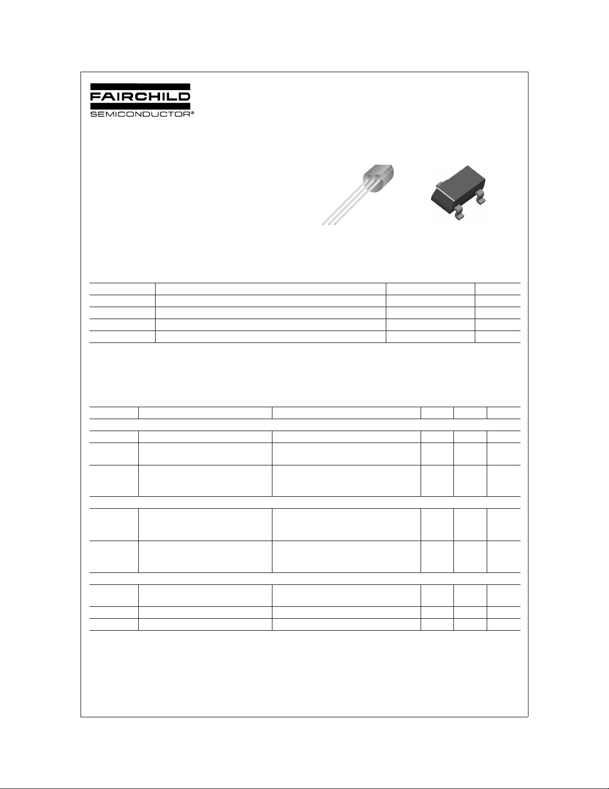
TO-92
3
2
1
SuperSOT-3
1. Drain 2. Source 3. Gate
Marking: I8
J108/J109/J110/MMBFJ108
Absolute Maximum Ratings * T
=25°C unless otherwise noted
A
Symbol Parameter Value Units
V
DG
V
GS
I
GF
, T
T
J
stg
* These ratings are limiting values above which the serviceability of any semiconductor device may be impaired.
NOTES:
1) These ratings are based on a maximum junction temperature of 150 degrees C.
2) These are steady state limits. The factory should be consulted on applications involving pulsed or low duty cycle operations.
Electrical Characteristics
Drain-Gate Voltage 25 V
Gate-Source Voltage -25 V
Forward Gate Current 10 mA
Operating and Storage Junction Temperature Range -55 ~ +150 °C
TA=25°C unless otherwise noted
Symbol Parameter Test Condition Min. Max. Units
Off Characteristics
V
(BR)GSS
I
GSS
(off) Gate-Sour ce C u t o ff Voltage VDS = 15V, ID = 10nA 108
V
GS
Gate-Source Breakdwon Voltage IG = -10µA, VDS = 0 -25 V
Gate Reverse Current VGS = -15V, VDS = 0
= -15V, VDS = 0, TA = 100°C
V
GS
109
110
-3.0
-2.0
-0.5
-3.0
-200
-10
-6.0
-4.0
On Characteristics
I
DSS
(on) Drain-Source On Resistance VDS ≤ 0.1V, VGS = 0 108
r
DS
Zero-Gate Voltage Drain Current * VDS = 15V, IGS = 0 108
109
110
109
110
80
40
10
8.0
12
18
Small Signal Characteristics
(on)
C
dg
C
(off)
sg
(on) Drain-Gate Off Capacitance VDS = 0, VGS = -10, f = 1.0MHz 15 pF
C
dg
(off) Source-Gate Off Capacitance VDS = 0, VGS = -10, f = 1.0MHz 15 pF
C
sg
* Pulse Test: Pulse Width ≤ 300µs, Duty Cycle ≤ 2.0%
Drain Gate & Source Gate On
Capacitance
= 0, VGS = 0, f = 1.0MHz 85 pF
V
DS
nA
nA
V
V
V
mA
mA
mA
Ω
Ω
Ω
©2002 Fairchild Semiconductor Corporation Rev. B1, November 2002

J108/J109/J110/MMBFJ108
Thermal Characteristics T
Symbol Parameter
P
D
R
θJC
R
θJA
* Device mounted on FR-4 PCB 1.6” × 1.6” × 0.06"
Total Device Dissipation
Derate above 25°C
Thermal Resistance, Junction to Case 125 °C/W
Thermal Resistance, Junction to Ambient 357 556 °C/W
=25°C unless otherwise noted
A
Max.
J108 - 1 10 *MMBFJ108
625
5.0
350
2.8
Units
mW
mW/°C
©2002 Fairchild Semiconductor Corporation Rev. B1, November 2002

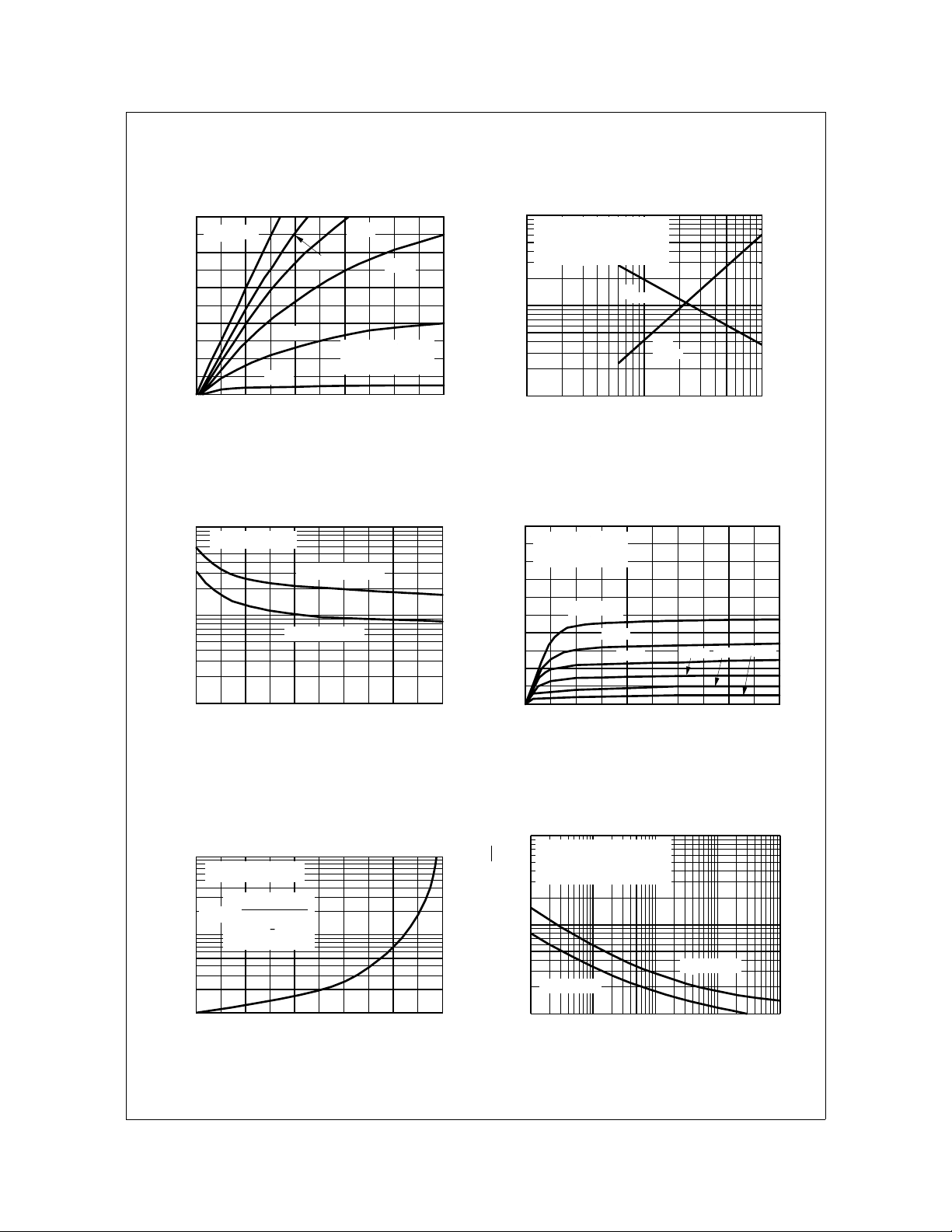
Typical Characteristics
J108/J109/J110/MMBFJ108
Common Drain-Source
100
V = 0 V
GS
80
60
40
20
D
I - DRAIN CURRENT (mA)
0
0 0.4 0.8 1.2 1.6 2
V - DRAIN-SOURCE VOLTAGE (V)
DS
- 4.0 V
- 5.0 V
- 2.0 V
- 1.0 V
TYP V = - 5.0 V
T = 25
A
GS(off)
- 3.0 V
캜캜캜캜
°°°°C
)
Ω
ΩΩ
Ω
100
(
DS
r - DRAIN "ON" RESISTANCE
Parameter Interactions
I @ V = 5.0V, V = 0 PULSED
DSS
r @ V = 100mV, V = 0
DS
50
V @ V = 5.0V, I = 3.0 nA
GS(off)
10
5
_
0.1 0.5 1 5 10
V - GATE CUTOFF VOLTAGE (V)
GS (OFF)
GS
DS
DS
DS
__
GS
D
r
DS
Figure 1. Common Drain-Source Figure 2. Parameter Interactions
Common Drain-Source
100
f = 0.1 - 1.0 MHz
C (V = 5.0V )
iss
DS
10
C (V = 0 )
rss
DS
rs
ts
C (C ) - CAPACITANCE (pF)
-20-16-12-8-40
V - GATE-SOURCE VOLTAGE (V)
GS
50
40
30
20
10
D
I - DRAIN CURRENT (mA)
Common Drain-Source
캜캜캜캜
T = 25
°°°°C
A
TYP V = - 0.7 V
GS(off)
V = 0 V
GS
- 0.1 V
- 0.2 V
0
012345
V - DRAIN-SOURCE VOLTAGE (V)
DS
1,000
I - DRAIN CURRENT (mA)
DSS
500
100
50
I
DSS
_
- 0.5 V
10
- 0.3 V
_
- 0.4 V
Figure 3. Common Drain-Source Figure 4. Common Dra in-Source
Normalized Drain Resistance
vs Bias Voltage
100
V @ 5.0V, 10
GS(off)
50
20
r =
DS
10
1 -
5
2
DS
1
r - NORMALIZED RESISTANCE
0 0.2 0.4 0.6 0.8 1
V /V - NORMALIZED GATE-SOURCE VOLTAGE (V)
GS
GS(off)
Figure 5. Normalized Drain Resistance vs
r
DS
V
GS
________
V
GS(off)
µµµµ
A
Noise Voltage vs Frequency
100
V = 10V
DG
√
√√
√
50
BW = 6.0 Hz @ f = 10 Hz, 100 Hz
= 0.21 @ f
10
5
I = 10 mA
n
e - NOISE VOLTAGE (nV / Hz)
1
0.01 0.03 0.1 0.5 1 2 10 100
Figure 6. Noise Voltage vs Frequency
≥≥≥≥
1.0 kHz
I = 1.0 mA
D
D
f - FREQUENCY (kHz)
Bias Voltage
©2002 Fairchild Semiconductor Corporation Rev. B1, November 2002
 Loading...