Denon DN-X1600 Service Manual
Ver. 3
Please refer to the
MODIFICATION NOTICE.
SERVICE MANUAL
MODEL JP E3 E2 EK K2A E1C E1K EUT
DN-X1600
P P
DJ MIXER
For purposes of improvement, specications and design are subject to change without notice.
•
Please use this service manual with referring to the operating instructions without fail.
•
Some illustrations using in this service manual are slightly different from the actual set.
•
D&M Holdings Inc.
S0144-1V03DM/DG1009
Copyright 2010 D&M Holdings Inc. All rights reserved.
WARNING: Violators will be prosecuted to the maximum extent possible.

SAFETY PRECAUTIONS
The following check should be performed for the continued protection of the customer and service technician.
LEAKAGE CURRENT CHECK
Before returning the unit to the customer, make sure you make either (1) a leakage current check or (2) a line to chassis
resistance check. if the leakage current exceeds 0.5 milliamps, or if the resistance from chassis to either side of the
power cord is less than 460 kohms, the unit is defective.
Be sure to test for leakage current with the AC plug in both polarities, in addition, in each power ON, OFF and STANDBY
mode, if applicable.
CAUTION
Heed the cautions!
◎
Spots requiring particular attention when servicing, such
as the cabinet, parts, chassis,etc., have cautions indicated
on labels. be sure to hee d these cau sions an d the
cautions indicated in the handling instructions.
Caution concerning electric shock!
◎
(1) An AC voltage is impressed on this set, so touching
internal metal parts when the set is energized could
cause electric shock. Take care to avoid el ectric
shock, by for example using an isolating transformer
and gloves when servicing while the set is energized,
unplugging the power cord when replacing parts, etc.
(2) Tere are high voltage parts inside. Handle with extra
care when the set is energized.
Please heed the points listed below during servicing and inspection.
◎ Caution concerning disassembly and
assembly!
Through great care is taken when manufacturing parts
from sheet metal, there may in some rare cases be burrs
on the edges of parts which could cause injury if ngers
are moved across them. Use gloves to protect your hands.
Only use designated parts!
◎
The set's parts have spe cific safety properties (fire
resistance, voltage resistance, etc.). For replacement
parts, be su re t o us e pa rt s wh ic h ha ve the same
poroperties. In particular, for the important safety parts
that are marked z on wiring diagrams and parts lists, be
sure to use the designated parts.
◎ Be sure to mount parts and arrange the wires
as they were originally!
For safety seasons, some parts use tape, tubes or other
insulating materials, and some parts are mounted away
from the surface of printed circuit boards. Care is also
taken with the positions of the wores omsode amd clamps
are used to keep wires away from heating and high
voltage parts, so be sure to set everything back as it was
originally.
Inspect for safety after servicing!
◎
Ch eck that al l screws , parts and wi res remove d or
disconnected for servicing have been put back in their
original positions, inspect that no parts around the area
that has been serviced have been negatively affected,
condu ct an insl at ion ch eck on t he ext er nal metal
connectors and between the blades of the power plug,
and otherwise check that safety is ensured.
(Insulation check procedure)
Unplug the power cord from the power outlet, disconnect
the antenna, plugs, etc., and turn the power switch on.
Using a 500V insulation resistance tester, check that the
inplug and the externally exposed metal parts (antenna
terminal, headphones terminal, input terminal, etc.) is
1MΩ or greater. If it is less, the set must be inspected and
repaired.
CAUTION
Concerning important safety
parts
Many of the electric and structural parts used in the set
have special saf ety properties. In most cases these
properties are difficult to distinguish by sight, and using
replacement parts with higher ratings (rated power and
withstand voltage) does not necessarily guarantee that
safety performance will be poreserved. Parts with safety
properties are indicated as shown below on the wiring
diagrams and parts lists is this service manual. Be sure to
replace them with parts with the designated part number.
(1) Schematic diagrams ......Indicated by the z mark.
(2)
Parts lists ......Indicated by the z mark.
Using parts other than the designated
parts could result in electric shock, res
or other dangerous situations.
2
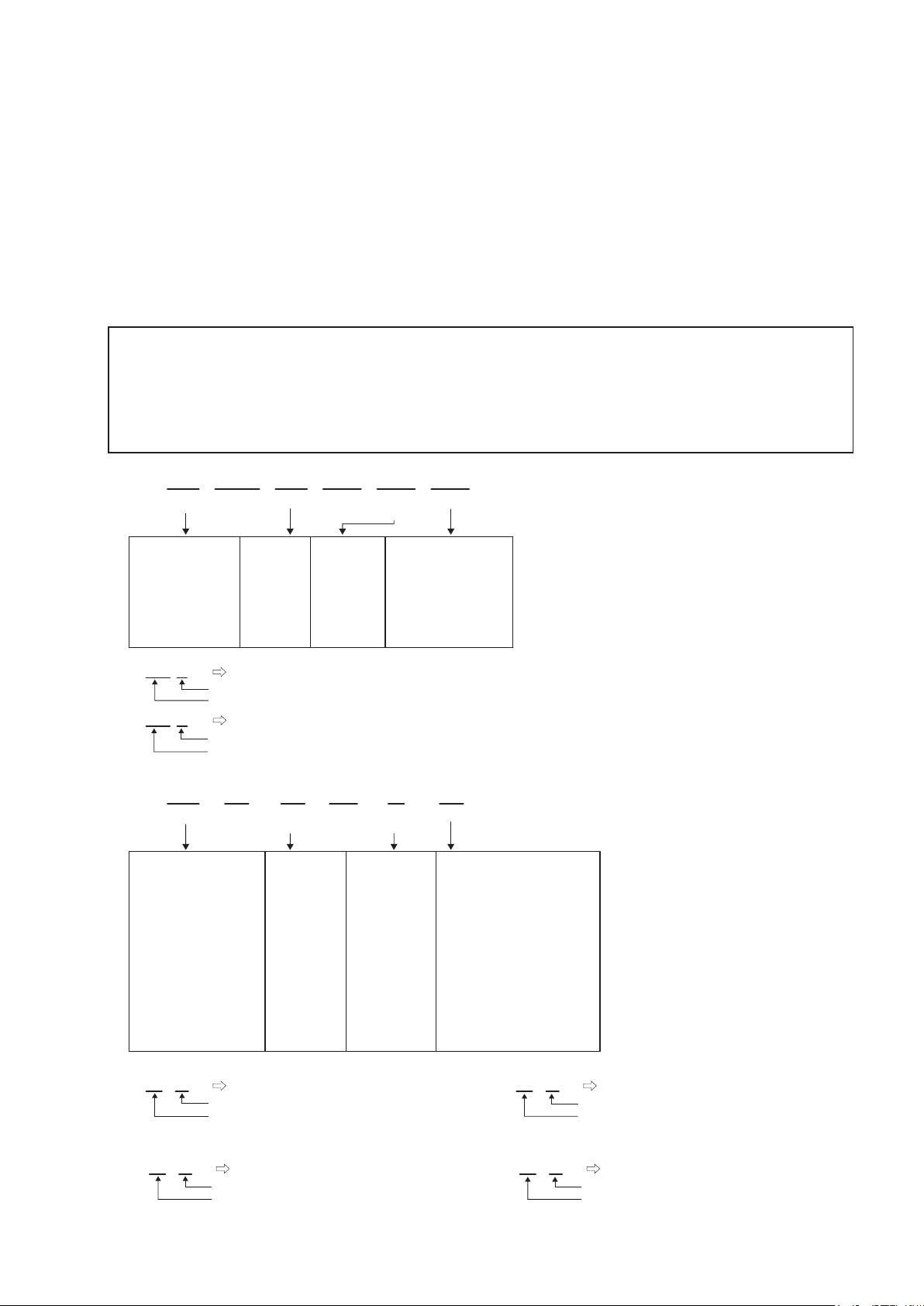
NOTE FOR SCHEMATIC DIAGRAM
NOTE FOR PARTS LIST
WARNING:
Parts marked with this symbol z have critical characteristics. Use ONLY replacement parts recommended by the manufacture
CAUTION:
Before returning the unit to the customer, make sure you make either (1) a leakage current check or (2) a line to chassis resistance check. If the
leakage current exceeds 0.5 milliamps, or if the resistance from chassis to either side of the power cord is less than 460 kohms, the unit is defective.
WARNING:
DO NOT return the unit to the customer until the problem is located and corrected.
NOTICE:
ALL RESISTANCE VALUES IN OHM. k=1,000 OHM / M=1,000,000 OHM
ALL CAPACITANCE VALUES IN MICRO FARAD. P=MICRO-MICRO FARAD EACH VOLTAGE AND CURRENT ARE MEASURED AT NO SIGNAL
INPUT CONDITION. CIRCUIT AND PARTS ARE SUBJECT TO CHANGE WITHOUT PRIOR NOTICE.
r.
NOTE FOR PARTS LIST
1.
Parts for which "nsp" is indicated on this table cannot be supplied.
2.
When ordering of part, clearly indicate "1" and "I" (i) to avoid mis-supplying.
3.
Ordering part without stating its part number can not be supplied.
4.
Part indicated with the mark "★" is not illustrated in the exploded view.
5.
Not including General-purpose Carbon Film Resistor in the P.W.Board parts list. (Refer to the Schematic Diagram for those parts.)
6.
Not including General-purpose Carbon Chip Resistor in the P.W.Board parts list. (Refer to the Schematic Diagram for those parts.)
WARNING:
● Resistors
Ex.: RN
* Resistance
Capacitors
●
Ex.: CE
* Capacity (electrolyte only)
* Capacity (except electrolyte)
・ When the dielectric strength is indicated in AC,"AC" is included after the dieelectric strength value.
Parts marked with this symbol z have critical characteristics. Use ONLY replacement parts recommended by the manufacturer.
Type
RD : Carbon
RC : Composition
RS : Metal oxide film
RW: winding
RN : Metal film
RK : Metal mixture
2
Indicates number of zeros after effective number.
2-digit effective number.
1-digit effective number.
: Units: ohm
Type
CE : Aluminum foil
electrolytic
CA : Aluminium solid
electrolytic
CS : Tantalum electrolytic
CQ : Film
CK : Ceramic
CC : Ceramic
CP : Oil
CM: Mica
CF : Metallized
CH : Metallized
2
Indicates number of zeros after effective number.
・ Units:μF.
・ Units:pF
2-digit effective number.
2
14K
Shape
and performance
2-digit effective number, decimal point indicated by R.
04W
Shape
and performance
Indicates number of zeros after efective number. (More than 2)
2-digit effective number.
2E
Power
2B : 1/8 W
2E : 1/4 W
2H : 1/2 W
3A : 1 W
3D : 2 W
3F : 3 W
3H : 5 W
1800ohm=1.8kohm1 8
1.2ohm1 R 2
1H
Dielectric
strength
0J : 6.3 V
1A : 10 V
1C : 16 V
1E : 25 V
1V : 35 V
1H : 50 V
2A : 100 V
2B : 125 V
2C : 160 V
2D : 200 V
2E : 250 V
2H : 500 V
2J : 630 V
2200μF2 2
2200pF=0.0022μF2 2
182
Resistance
F : ±1%
G : ±2%
J : ±5%
K : ±10%
M : ±20%
3R2
CapacityMAllowable
G
Allowable
error
P : Pulse-resistant type
NL : Low noise type
NB : Non-burning type
FR : Fuse-resistor
F : Lead wire forming
error
F : ±1%
G : ±2%
J : ±5%
K : ±10%
M : ±20%
Z : ±80%
: - 20%
P : +100%
C : ±0.25pF
D : ±0.5pF
= : Others
FR
Others
BP
Others
HS : High stability type
BP : Non-polar type
HR : Ripple-resistant type
DL : For change and discharge
HF : For assuring high requency
U : UL part
C : CSA part
W : UL-CSA part
F : Lead wire forming
2
・ Units:μF.
1
・ Units:pF
2.2μF2 R
1-digit effective number.
2-digit effective number, decimal point indicated by R
220pF2 2
Indicates number of zeros after effective numver. (0 or 1)
2-digit effective number.
3
TECHNICAL SPECIFICATIONS
n AUDIO (0 dBu = 0.775 Vrms, 0 dBV = 1 Vrms)
• PHONO inputs Stereo x 3 Unbalanced RCA terminal
Input impedance: 47 kΩ/kohms
Level: –40 dBV (10 mV)
• CD inputs Stereo x 5 Unbalanced RCA terminal
Input impedance:
Level: 0 dBV
• Equalizer (LINE) Band x 3
Channel equalization adjustment range:
HI: –∞,–90 dB to +10 dB
MID: –∞,–90 dB to +10 dB
LOW: –∞,–90 dB to +6 dB
• RETURN inputs Monaural x 2 1/4" TS terminal
Input impedance: 10 kΩ/kohms
Level: –10dBV/0dBV (Default: –10dBV)
• MIC inputs Monaural x 2
MIC1: Balanced XLR
(1: Ground, 2: Hot, 3: Cold)
MIC2: Balanced 1/4" TRS jack
(Tip: hot, ring: cold, sleeve: ground)
Input impedance: 5 kΩ
Level: –60 to –20 dBu
EIN:
CMRR: More than 89 dB (1 kHz)
• Equalizer (MIC) Band x 2
Adjustment range: HI: –15 to +15 dB
LOW: –15 to +15 dB
• USB audio inputs
Fs: 44.1 kHz, 48 kHz, 96 kHz USB B
• MASTER output
Balanced: Stereo, balanced XLR terminal
(1: Ground, 2: Hot, 3: Cold)
DA converter: 32-bit 128x oversampling advanced
Load impedance: More than 600 Ω
Level: +4dBu (Max.: +24 dBu)
Frequency response: 20 Hz to 20 kHz (±0.5 dB)
THD: Less than 0.05%
Crosstalk: Less than –100 dB (1 kHz)
Unbalanced: Stereo RCA terminal
Load impedance: 10 kΩ
Level: 0 dBu (Max.: +20 dBu)
• REC output Stereo Unbalanced RCA terminal
Load impedance: 10 kΩ
Level: –10 dBV (Max.: +10 dBV)
• BOOTH output Stereo
(Tip: hot; ring: cold, sleeve: ground)
Load impedance: More than 600 Ω
Level: +4 dBu (Max.: +24 dBu)
• SEND output Monaural x 2
Load impedance: 10 kΩ
Level: –10 dBV (Max.: +10 dBV)
• Headphones output Stereo
Load impedance: 40 Ω
Level: 150 mW
• Digital coaxial output
(Fs: 44.1 kHz, 48 kHz, 96 kHz)
• USB audio output Stereo x 4 (monaural x 8) 24 bit,
44.1 kHz, 48 kHz, 96 kHz USB B
10 kΩ/kohms
Less than –126 dBu (Rs = 150 Ω)
Stereo x 4 (monaural x 8) 24 bit,
segment converter
Balanced 1/4" TRS terminal
Unbalanced 1/4" TS terminal
Stereo RCA terminal, IEC958 Consumer
n GENERAL
USB MIDI I/O: IN: 1ch, OUT: 1ch MIDI1.0,
MIDI Clock USB B
MIDI OUT: OUT: 1ch MIDI1.0,
MIDI Clock 5pin DIN
Channel level meters:
peak display
Cue master level meters:
peak display
Channel Fader: 60 mm Slim Type fader
Crossfader:
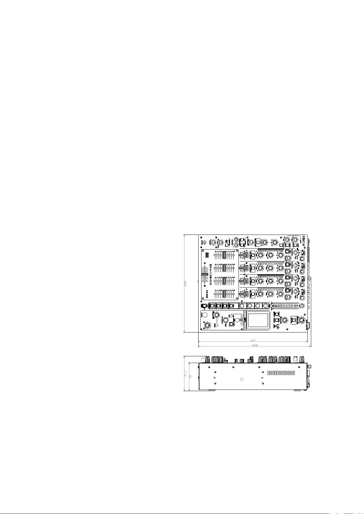
Dimensions: 320(W) x 357(D) x 91(H) mm
Weight: 6.2 Kg (13.7 lbs)
Supply voltage: AC 120 V, 60 Hz(U.S.A. and Canada
AC 230 V, 50 Hz (European models)
Power consumption: 34 W
Operational temperature:
+5ºC to +35ºC(+41 F to +95 F)
Operational humidity: 25% to 85%
Storage temperature: –20ºC to +60ºC(-4 F to +140 F)
n DIMENSION
PPM 16-point LEDs from –40 to +10 dB,
PPM 16-point LEDs from –40 to +10 dB,
45 mm FLEX Fader (Fader Torque Adjustable)
(12”5/8 (W) x 14”1/16 (D) x 3”5/8 (H))
models)
4
DISASSEMBLY
• Disassemble in order of the arrow of the gure of following ow.
• In the case of the re-assembling, assemble it in order of the reverse of the following ow.
• In the case of the re-assembling, observe "attention of assembling" it.
• If wire bundles are untied or moved to perform adjustment or parts replacement etc., be sure to rearrange them neatly
as they were originally bundled or placed afterward.
Otherwise, incorrect arrangement can be a cause of noise generation.
TOP CHASSIS SUB ASSY
Refer to "DISASSEMBLY
1.TOP CHASSIS SUB ASSY"
and "EXPLODED VIEW"
TOP PANEL UNIT INPUT UNIT FADER UNIT
Refer to "DISASSEMBLY Refer to "DISASSEMBLY Refer to "DISASSEMBLY
2.TOP PANEL UNIT" 3. INPUT UNIT" 5. FADER UNIT"
and "EXPLODED VIEW" and "EXPLODED VIEW" and "EXPLODED VIEW"
PANEL1 UNIT INPUT UNIT CH FADER UNIT
(Ref. No. of EXPLODED VIEW : B-1) (Ref. No. of EXPLODED VIEW : D) (Ref. No. of EXPLODED VIEW : C-3~6)
EFFECT UNIT FLAX FADER UNIT
(Ref. No. of EXPLODED VIEW : F) (Ref. No. of EXPLODED VIEW : 55)
SPLIT UNIT OUTPUT UNIT, MAIN UNIT
(Ref. No. of EXPLODED VIEW : B-2) Refer to "DISASSEMBLY
4. OUTPUT UNIT, MAIN UNIT" HP UNIT
and "EXPLODED VIEW" Refer to "DISASSEMBLY
OUTPUT UNIT 6. HP UNIT"
(Ref. No. of EXPLODED VIEW : E-1) and "EXPLODED VIEW"
MAIN UNIT HP UNIT
(Ref. No. of EXPLODED VIEW : F) (Ref. No. of EXPLODED VIEW :C-2)
MIC UNIT
Refer to "DISASSEMBLY
7. MIC UNIT"
and "EXPLODED VIEW"
MIC UNIT
(Ref. No. of EXPLODED VIEW : E-2)
AC INPUT UNIT
Refer to "DISASSEMBLY
8. AC INPUT UNIT"
and "EXPLODED VIEW"
AC INPUT UNIT
(Ref. No. of EXPLODED VIEW : A-1)
POWER UNIT
Refer to "DISASSEMBLY
9. POEWR UNIT"
and "EXPLODED VIEW"
POWER UNIT
(Ref. No. of EXPLODED VIEW : A-2)
5
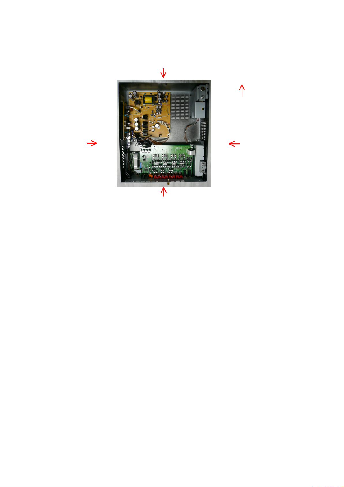
About the photos used for descriptions in the DISASSEMBLY" section.
• The direction from which the photographs used herein were photographed is indicated at "Direction of photograph:
***" at the left of the respective photographs.
• Refer to the table below for a description of the direction in which the photos were taken.
• Photographs for which no direction is indicated were taken from above the product.
The viewpoint of each photograph
(Photografy direction)
[View from above]
Direction of photograph: C
Direction of photograph: B
Front side
Direction of photograph: D
Direction of photograph: A
6
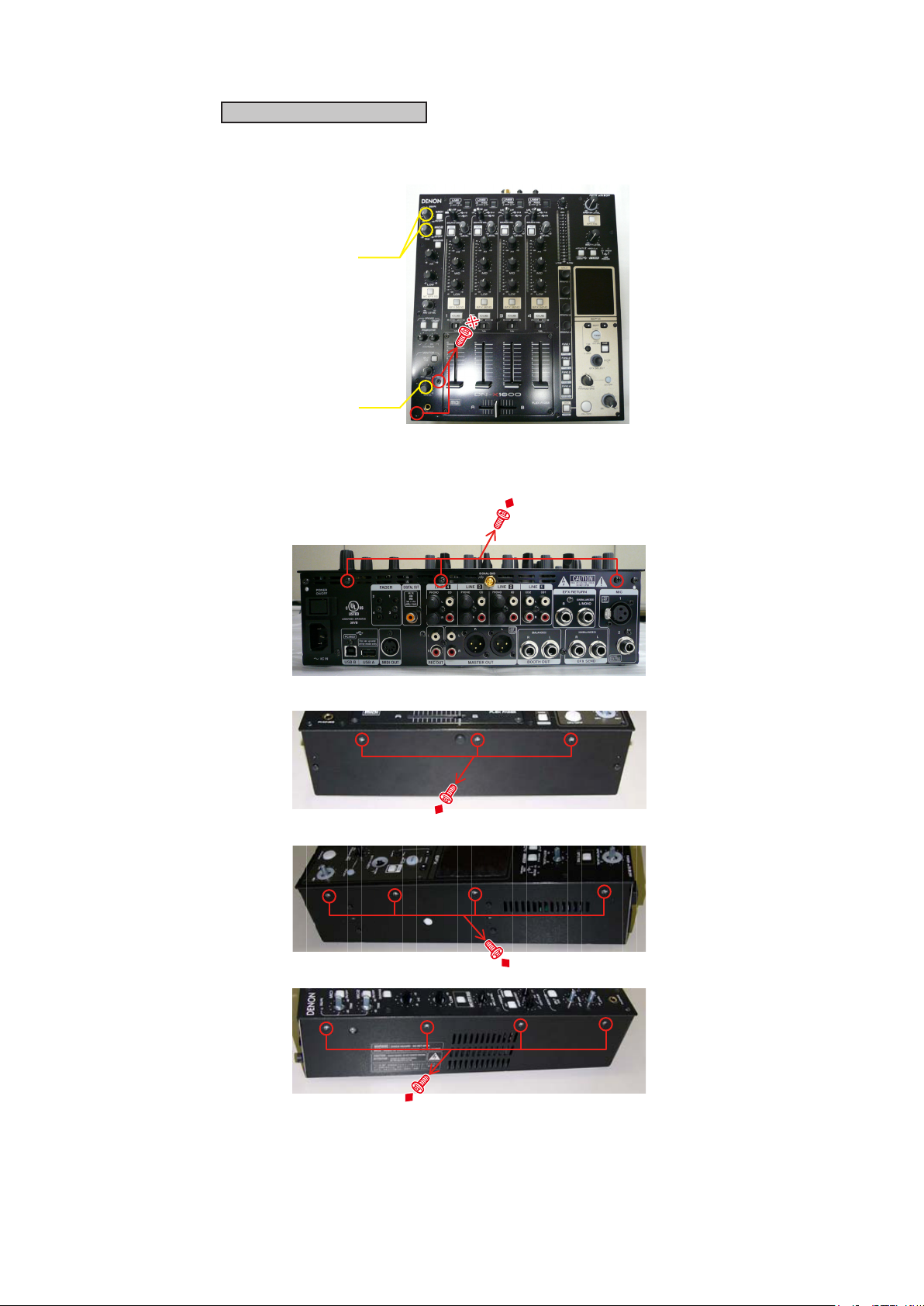
1. TOP CHASSIS SUB ASSY
Proceeding : TOP CHASSIS SUB ASSY
(1) Remove the screws and the knobs.
KNOB
KNOB
(2) Remove the screws.
Direction of photograph: A
Direction of photograph: B
Direction of photograph: C
Direction of photograph: D
7
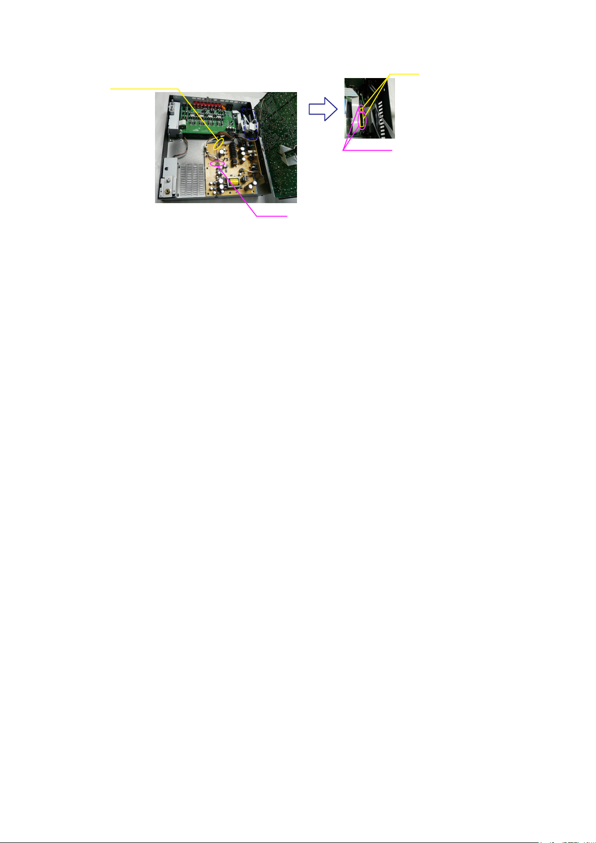
(3) Disconnect the connector wire and FFC Cable, and remove the sheet. Open the wire clamper.
SHEET
WIRE CLAMPER
FFC Cable
Direction of photograph: B
CX071
8
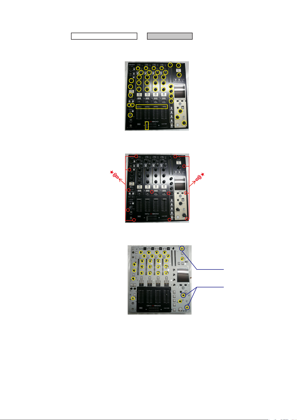
2. TOP PANEL UNIT
Proceeding : TOP CHASSIS SUB ASSY
(1) Remove the knobs.
(2) Remove the screws.
TOP PANEL UNIT
→
(3) Remove the Nuts and Lens rings.
LENS RING
LENS RING
9
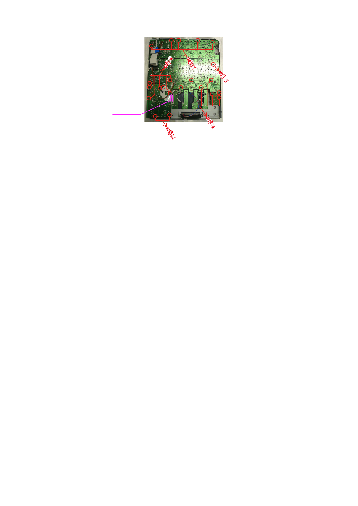
(4) Disconnect the FFC Cable. Remove the secrews.
FFC Cable
10
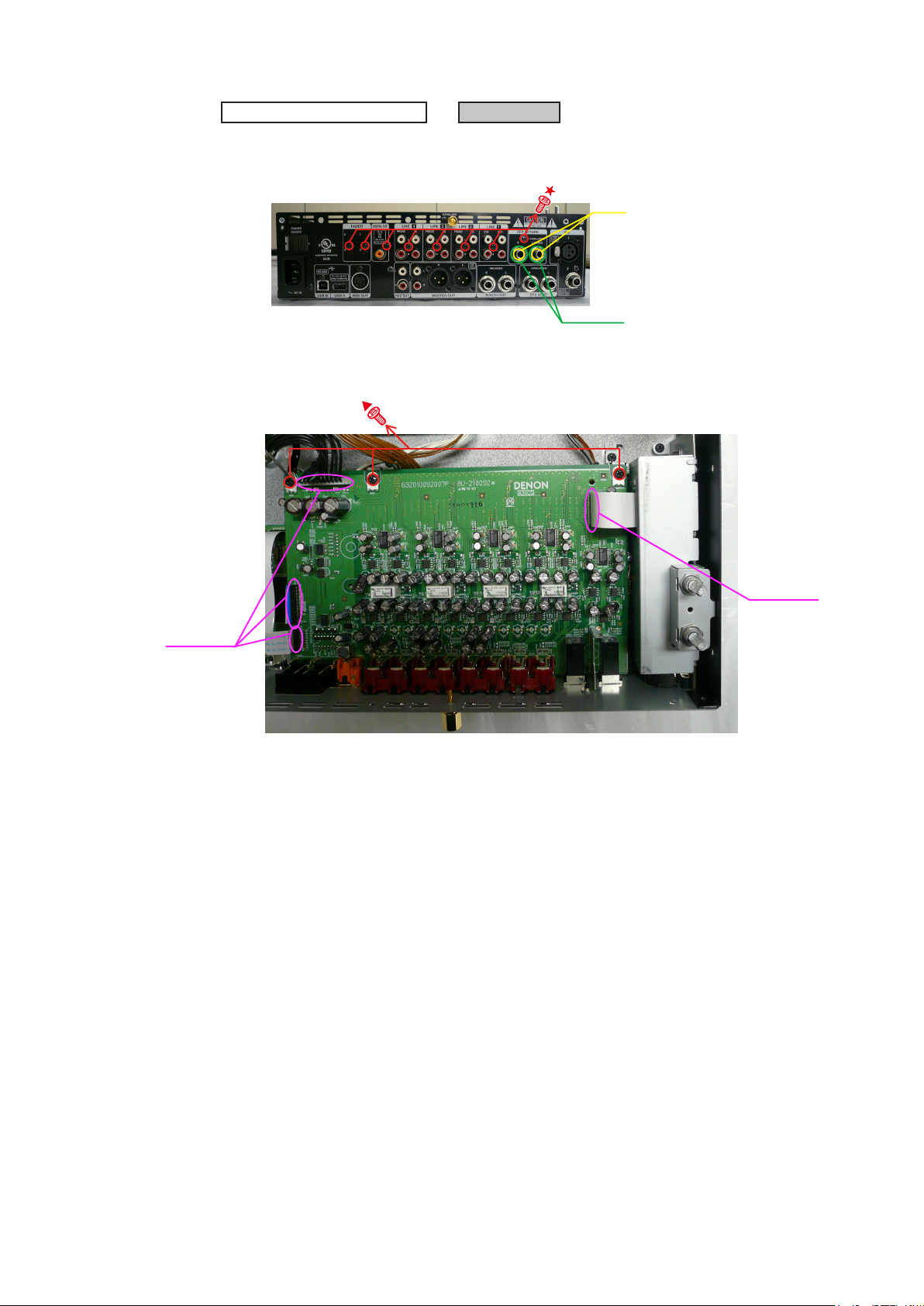
3. INPUT UNIT
Proceeding : TOP CHASSIS SUB ASSY
(1) Remove the screws. Remove the Nuts and Washers.
Direction of photograph: A
(2) Remove the screws.Disconnect the FFC Cables.
→
INPUT UNIT
NUT
WASHER
FFC Cable
FFC Cable
11
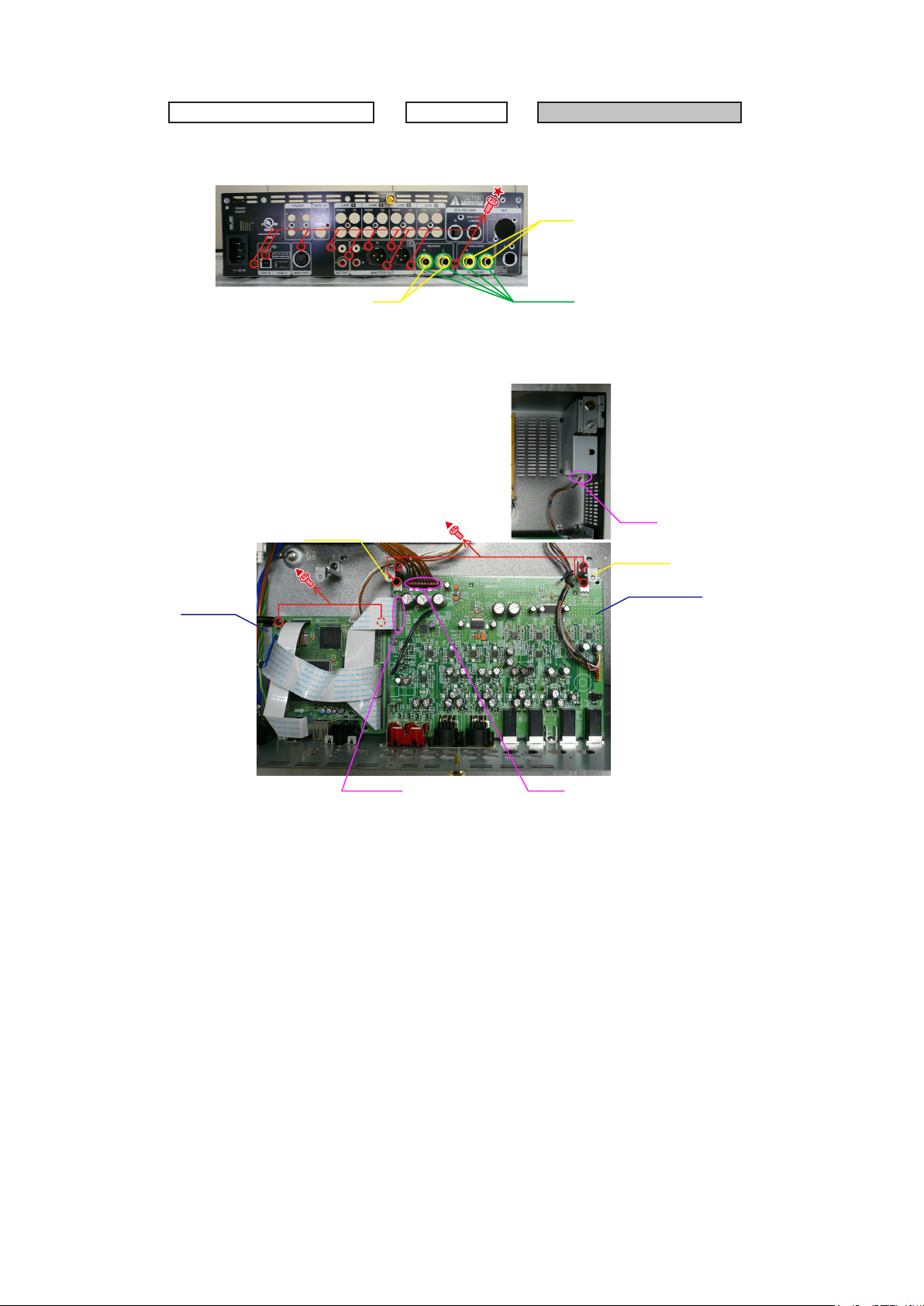
4. OUTPUT UNIT, MAIN UNIT
Proceeding : TOP CHASSIS SUB ASSY
(1) Remove the screws. Remove the Nuts and Washers.
Direction of photograph: A
(2) Remove the screws. Disconnect the FFC Cables and the connectors.
STAY PWB
INPUT UNIT
→
OUTPUT UNIT, MAIN UNIT
→
NUT
WASHERNUT
CY102
STAY PWB
MAIN UNIT
OUTPUT UNIT
FFC Cable CX101
12
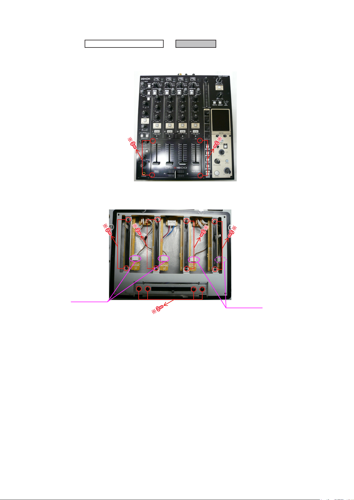
5. FADER UNIT
Proceeding : TOP CHASSIS SUB ASSY
(1) Remove the screws.
(2) Remove the screws. Disconnect the connector wires.
→
FADER UNIT
CONNECTOR
CONNECTOR
13
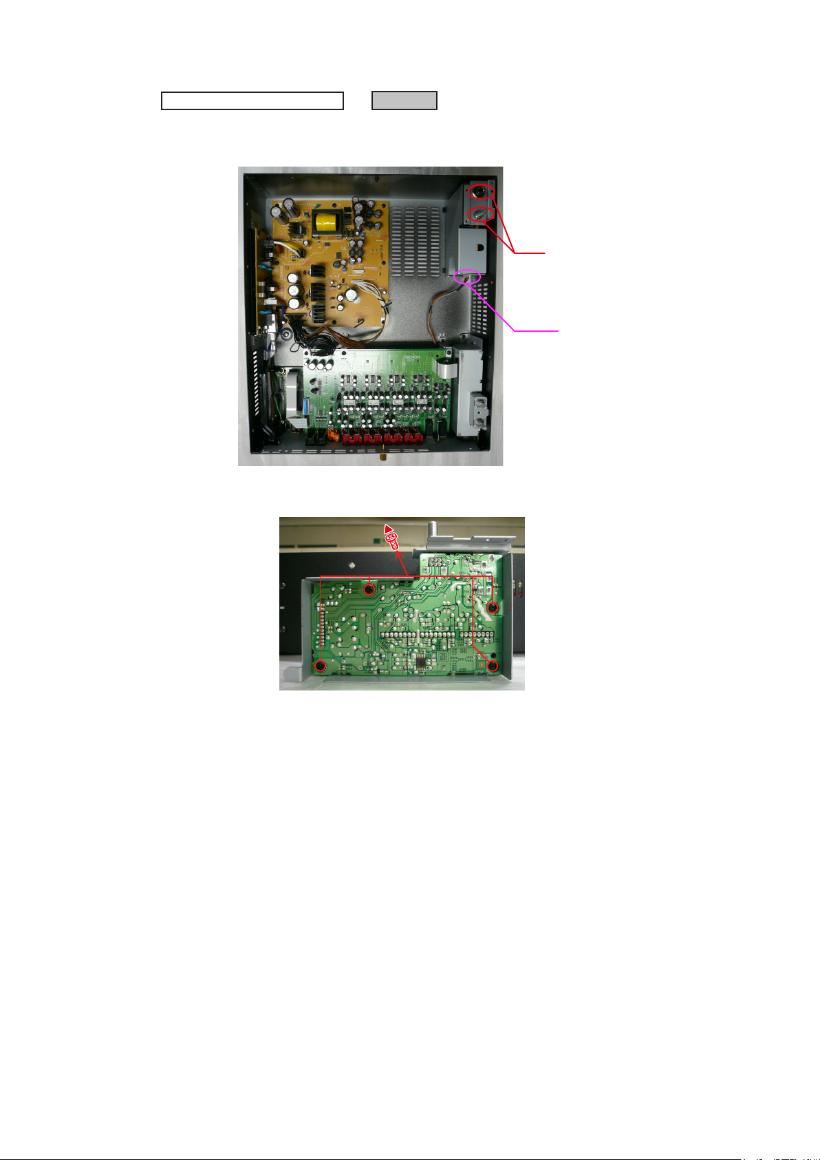
6. HP UNIT
Proceeding : TOP CHASSIS SUB ASSY
(1) Disconnect the connector wire. Remove the Nuts.
→
HP UNIT
NUT
CY102
(2) Remove the screws.
Direction of photograph: D
14
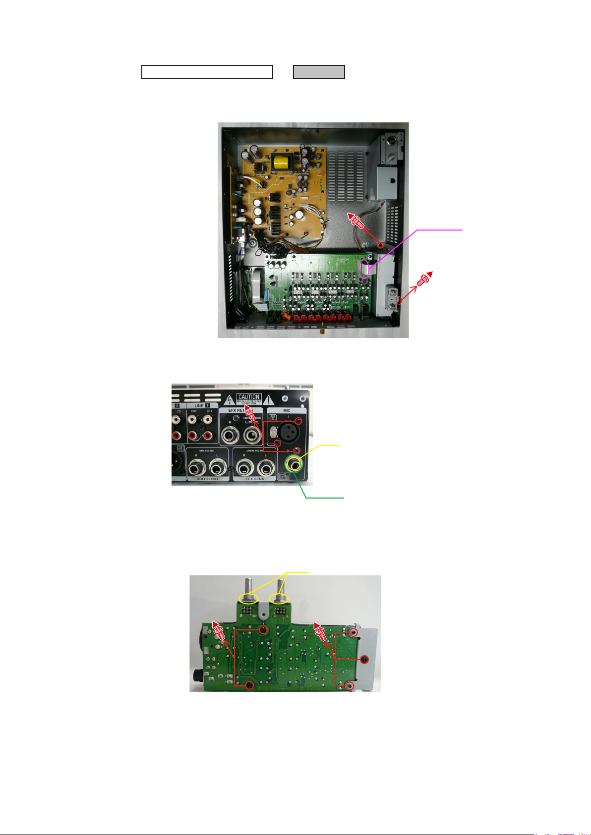
7. MIC UNIT
Proceeding : TOP CHASSIS SUB ASSY
(1) Remove the screw. Disconnect the FFC Cable.
→
MIC UNIT
FFC Cable
(2) Remove the screws. Remove the Nut and Washer.
Direction of photograph: D
(3) Remove the screws.
Direction of photograph: D
NUT
WASHER
NUT
15
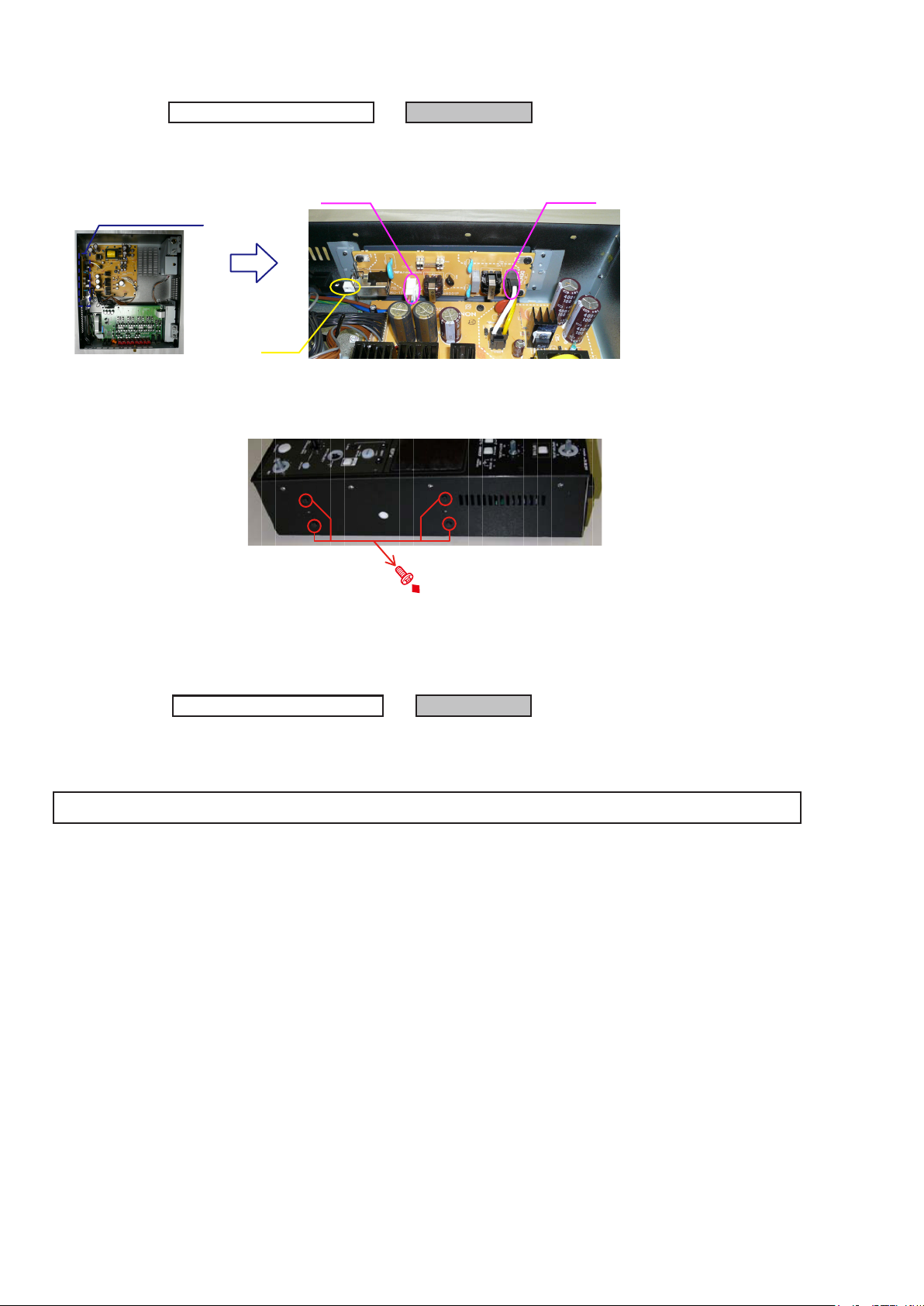
8. AC INPUT UNIT
Proceeding : TOP CHASSIS SUB ASSY
(1) Disconnect the connector wires and LINK.
AC INPUT UNIT
→
AC INPUT UNIT
(2) Remove the screws.
Direction of photograph: C
LINK
CX021
CX022
Direction of photograph: D
9. POWER UNIT
Proceeding : TOP CHASSIS SUB ASSY
Please refer to "EXPLODED VIEW" for the disassembly method of POWER P.W.B. UNIT.
POWER UNIT
→
16

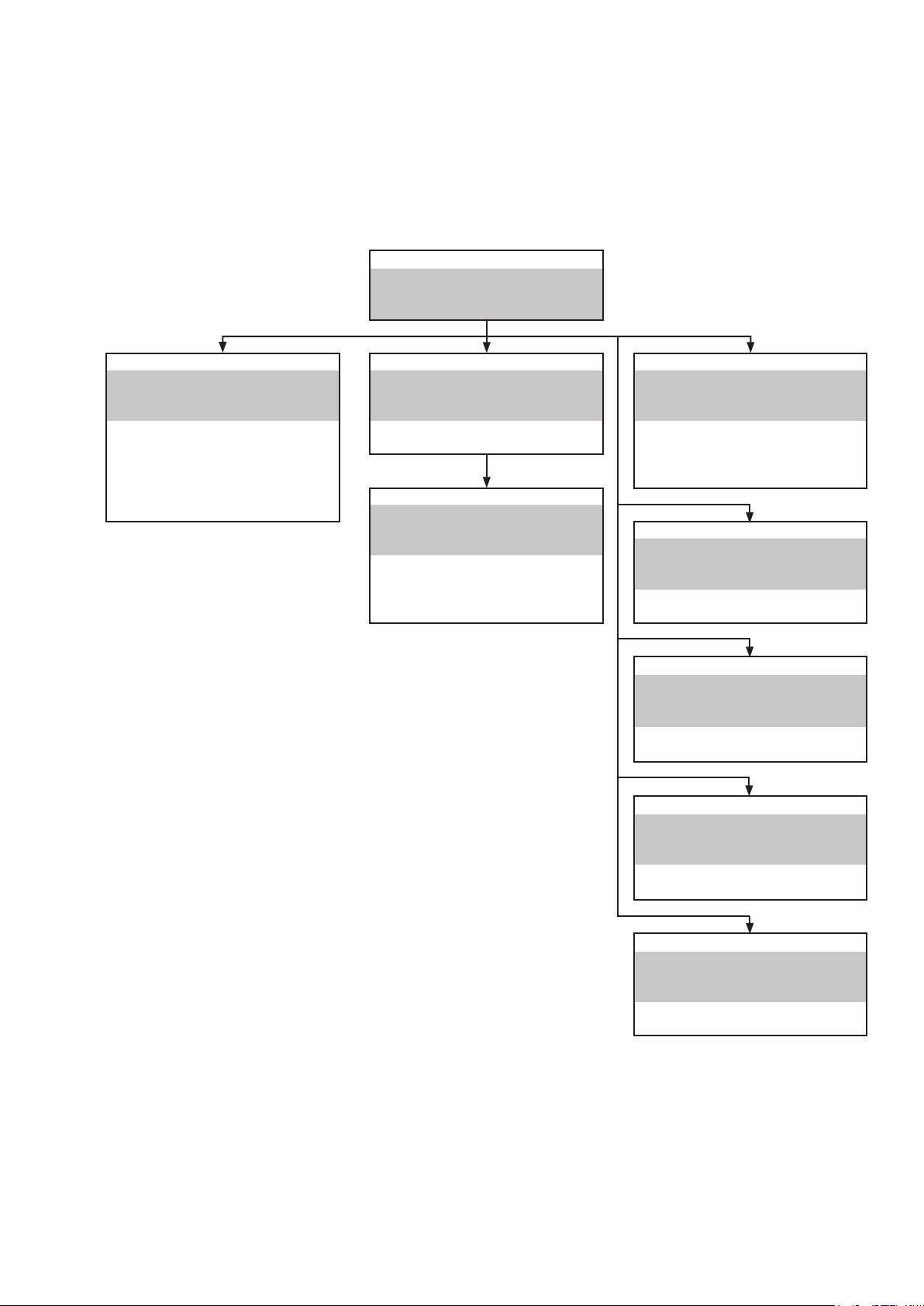
SERVICE MODE
1. Launching the service mode and selecting the check mode
PressingtheMIC1ON/OFFandMICEFXINSbuttonsimultaneously,turnonthepower.KeeppressingtheMIC1ON/
・
OFFandMICEFXINSbuttonuntil[DENON]isdisplayed.Whentheservicemodeisset,theservicemode'stopmenu
appears.
Thecommunicationsmodeissetwhenthepoweristurnedoffthenturnedbackon.
※
Contentsofthedisplayontheservicemode'stopmenu
・
1)Func
2)SWChk
3)VRChk
4)LEDChk
TurntheEFXSELECTcontroltoselecteachcheckmode,thenpresstheEFXSELECTcontroltoseteachcheck
・
mode.
2. Mode
2.1. Func (Function Mode)
With "Func" is displayed, press the EFX SELECT control.
(Items marked * are for design inspection. Do not use them for servicing purposes.)
・ Contentsofthedisplayonthefunctionmode'smenu
1)USBR/W
2)MIDIout
3)ROM/RAM
4)Initial
Thecontentsofthepresetmemoryaresettothefactorydefaults.
①
②
③
5)RunTime
①
Tocleartheaccumulatedpowerontime.
・
②
③
④
6)Version
Firmwareversionisdisplayed.
「
「
*(fordesigninspection)
*(fordesigninspection)
*(fordesigninspection)
"Cancel"isdisplayedinash.
TurntheEFXSELECTcontroltoselect"OK".
With"OK"displayedinash,presstheEFXSELECTcontroltoexecuteinitialization."Done!"isdisplayedwhen
initializationiscompleted.
WhenpresstheEFXSELECTcontrol,accumulatedpowerontimeisdisplayed.(Max:65000h
PresstheEFXSELECTcontrolwithaccumulatedpowerontimeisdisplayed,"Clear?"isdisplayed.
TurntheEFXSELECTcontroltoselect"OK".
With"OK"isdisplayedinash,presstheEFXSELECTcontroltoerasethetotaltimeofpoweron."Done!"is
displayedwhenerasureiscompleted.
SYS****
DSP****
」
」
)
PresstheTime(Back)buttontoreturntothetopmenuoftheservicemode.
2.2. SW Chk (Panel switch Check)
With "SW Chk" is displayed, press the EFX SELECT control
Checktheoperationsoftheswitches.
・
1)Intheinitialstatus,characterisdisplayedontheVFD.
2)Whenaswitchispressed,thecharactercorrespondingtotheswitchdisappears.
3)Whenallswitchesarepressed,"Finish!"isdisplayed.
4)PresstheEFXSELECTcontrolwith"Finish!"isdisplayedtoreturntothetopmenuoftheservicemode.
WhentheTAPbuttonispressedwhilethe"SWChk"modeisbeingexecuted,theservicemode'stopmenu
※
reappears.
PresstheTime(Back)buttontoreturntothetopmenuoftheservicemode.
17

2.3. VR Chk (Panel volume Check))
With "VR Chk" is displayed, press the EFX SELECT control
ChecktheoperationsoftheVR.
・
TurntheVR,VRnameandvalueof"0"~"1023"aredisplayedontheVFD.
Checktheoperationsoftherotaryencoder.
・
Whentherotaryencoderisturned,therotaryencodernameand"<"(counterclockwise)or">"(clockwise)are
displayedontheVFD.
Whentherotaryencoderwithaswitchispressed,therotaryencodernameand“■”aredisplayedontheVDF.
ChecktheoperationsofthefaderVR.
・
MovethefaderVR,faderVRnameandvalueof"0"~"1023"aredisplayedontheVFD.
ChecktheoperationsoftheslideSW.
・
MovetheslideSW,slideSWnameand"A"(Left),"T"(Center),"B"(Right)aredisplayedontheVFD.
Note:TheheadphonesLEVEL,MIC1TRIM,MIC2TRIMcontrolareananalogVR,sothereisnoVRnameandvalue
display.
PresstheTime(Back)buttontoreturntothetopmenuoftheservicemode.
2.4. LED Chk (Panel LED Check)
With "LED Chk" is displayed, press the EFX SELECT control
(Items marked * are for design inspection. Do not use them for servicing purposes.)
CheckthelightingoftheLED.
・
WhentheTAPbuttonispressed,themodechangesintheordershownbelow.
1)ALLLight:AllLEDsLight.
2)Dimmer:ThedimmerfunctionLEDsaresettothedimmerlitstatus.
CUE1、CUE2、CUE3、CUE4、EFEXSEND(LINE1)、EFEXSEND(LINE2)、EFEXSEND(LINE3)、EFEX
SEND(LINE4)、CUE(EFX)、EFEXON/OFF、PARAMETERSON/OFF
3)Green:OnlygreenLEDlight.
4)Amber:OnlyorangeLEDlight.
5)Red:OnlyredLEDlight.
6)Blue:OnlyblueLEDlight.
7)MaxON
8)Typical*:Fixedformloadlighting(fordesigninspection)
Maximumloadlighting(fordesigninspection)
*:
PresstheTime(Back)buttontoreturntothetopmenuoftheservicemode.
18
VERSION UPGRADE PROCEDURE OF FIRMWARE
Usetheproceduredescribedbelowtoupdatethermwaretoanewerversion.
Storetheleforupdatingthermware(lename:X1600FW.BIN)intherootdirectoryofUSBdevice.
・
IftheleforupdatingthermwareisstoredonaUSBdevice,connecttheUSBdevicetotheUSBAterminal.
・
Note:DonotturnoffthepowerordisconnecttheUSBcableortheUSBdevicewhilethermwareisbeingupdated.
Ifrmwareupdatingisnotcompletednormally,someoperationsmaynolongerbeguaranteedtoworkanditmay
notbepossibletoupdatethermwareagain.
1)TurnonthepowerwhilepressingtheMIC2ON/OFFandDUCKINGbuttonsimultaneously.(Versionupmode)
2)PresstheUTILITYbuttonaccordingtothescreendisplay.
3)"****->****"isscrolldisplayed.
4)PresstheMIDICLKbuttontobeginupdating.(Approximately40secondarerequiredforupdatingtobecompleted.)
5)"Finish!"and"Ver****"aredisplayedwhenrmwareupdatingiscompleted.
6)TurnthepoweroffanddisconnecttheUSBdevicefromtheUSBport.
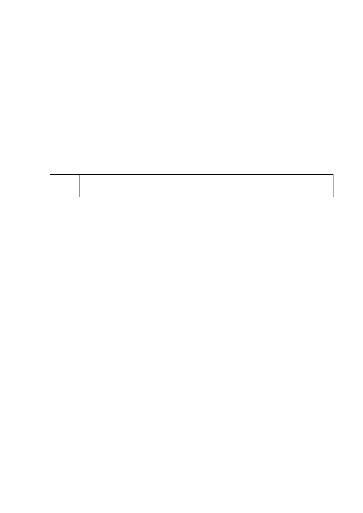
ABOUT REPLACE THE MICROPROCESSOR WITH A NEW ONE
WhenreplacedoftheU-PRO(Microprocessor)ortheFlashROM,conrmcontentsofthefollowing.
PWB Name Ref. No. Description
MAIN IC103 EN29LV160BB-70TIP B FILENAME:X1600FW.BIN
Afterreplaced
A:MaskROM(Withsoftware).Noneedwrite-inofsoftwaretothemicroprocessor.
B:FlashROM(Withsoftware).Usually,noneedwrite-inofsoftware.But,whenthesoftwarewasupdated,youshouldbe
write-inofthenewsoftwaretothemicroprocessororashROM.Pleasecheckthesoftwareversion.
C:EmptyFlashROM(Withoutsoftware).Youshouldbewrite-inofthesoftwaretothemicroprocessororashROM.
Referto"Updateprocedure"or"writingprocedure",whenyoushouldbewrite-inthesoftware.
After
replaced
Remark
19
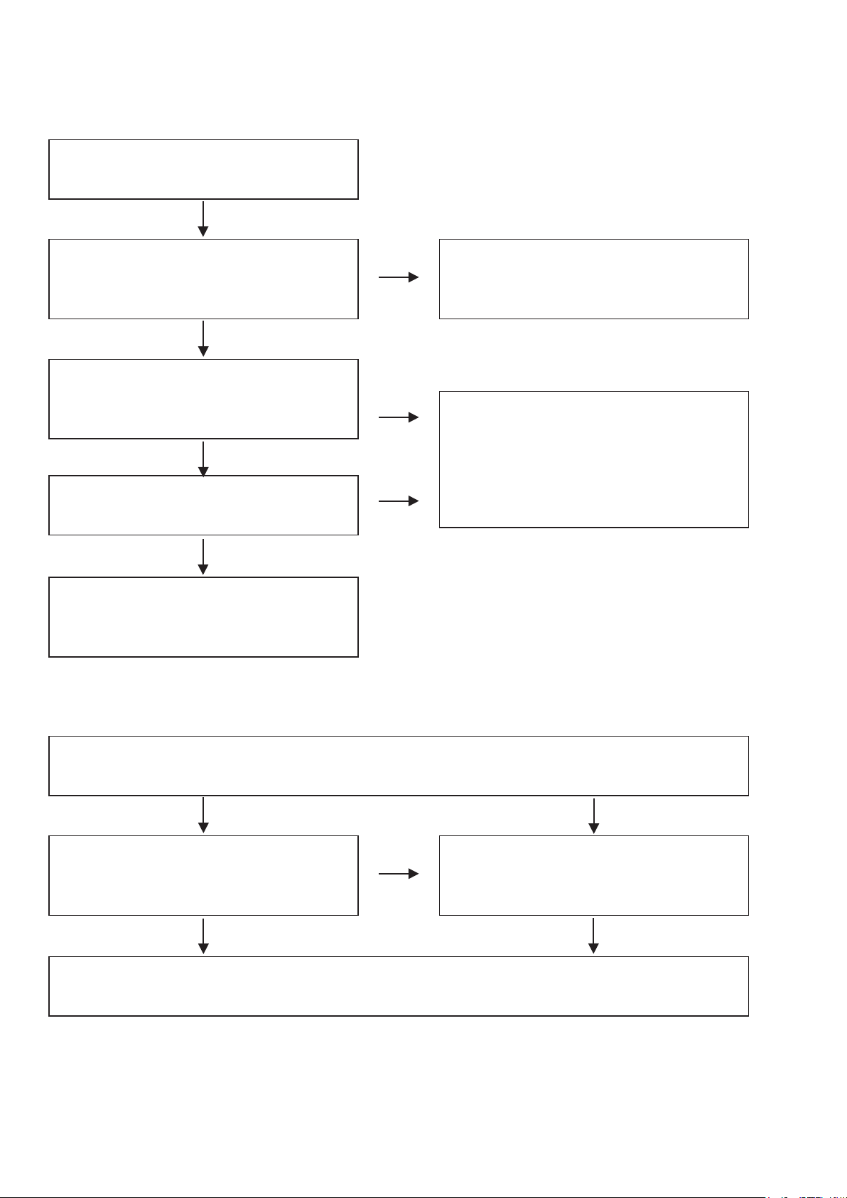
TROUBLE SHOOTING
FLOW CHART NO.1 (8U-110068-1, -2:POWER UNIT)
The power cannot be turned on.
O.K.
N.G.
Is the fuse normal? See FLOW CHART NO.2 <The fuse blows out.>
O.K.
Is normal state restored when once unplugged
power cord is plugged again after several seconds?
O.K.
Is the +3.3V line voltage normal?
O.K.
Check each rectifying circuit of the secondary
circuit and replace it if defective.
FLOW CHART NO.2 (8U-110068-1, -2:AC INPUT UNIT, POWER UNIT)
The fuse blows out.
N.G.
N.G.
Check if there is any leak or short-circuiting on
the primary circuit component, and replace it if
defective.
(C901,C902,C903,C906,C907,C908,L901,L902,T901
)
O.K.
Check the presence that the primary component
is leaking or shorted and replace it if defective.
O.K.
After servicing, replace the fuse.
N.G.
20
O.K.
Check the presence that the rectifying diode
or circuit is shorted in each rectifying circuit of
secondary side, and replace it if defective.
O.K.
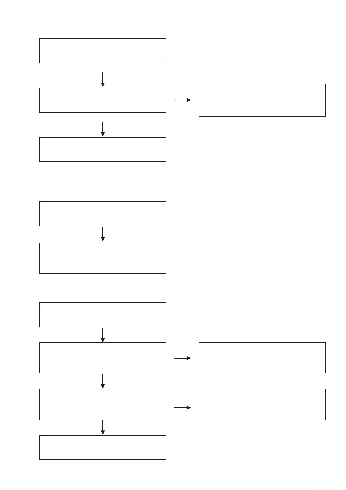
FLOW CHART NO.3 (8U-110068-1, -2:POWER UNIT)
+1.2V is not outputted.
O.K.
Is the +5V line voltage normal?
O.K.
Check IC903 and the periphery circuit, and replace
it if defective
FLOW CHART NO.4 (8U-110068-1, -2:POWER UNIT)
+3.3V is not outputted.
O.K.
See FLOW CHART
NO.1 <Is the +3.3V line voltage normal?>
N.G.
Check if there is any leak or short-circuiting on the
primary circuit component, and replace it if
defective.
(C901,C902,C903,C906,C907,C908,L901,L902,T901)
FLOW CHART NO.5 (8U-110068:POWER UNIT)
+15VA is not outputted.
O.K.
Is the fuse normal? See FLOW CHART NO.2 <The fuse blows out.>
O.K.
Is the voltage of +15V or more supplied to IN
terminal of IC907
O.K.
Check IC907 and the periphery circuit, and replace
it if defective.
N.G.
N.G.
Check D924 and replace it if defective.
21
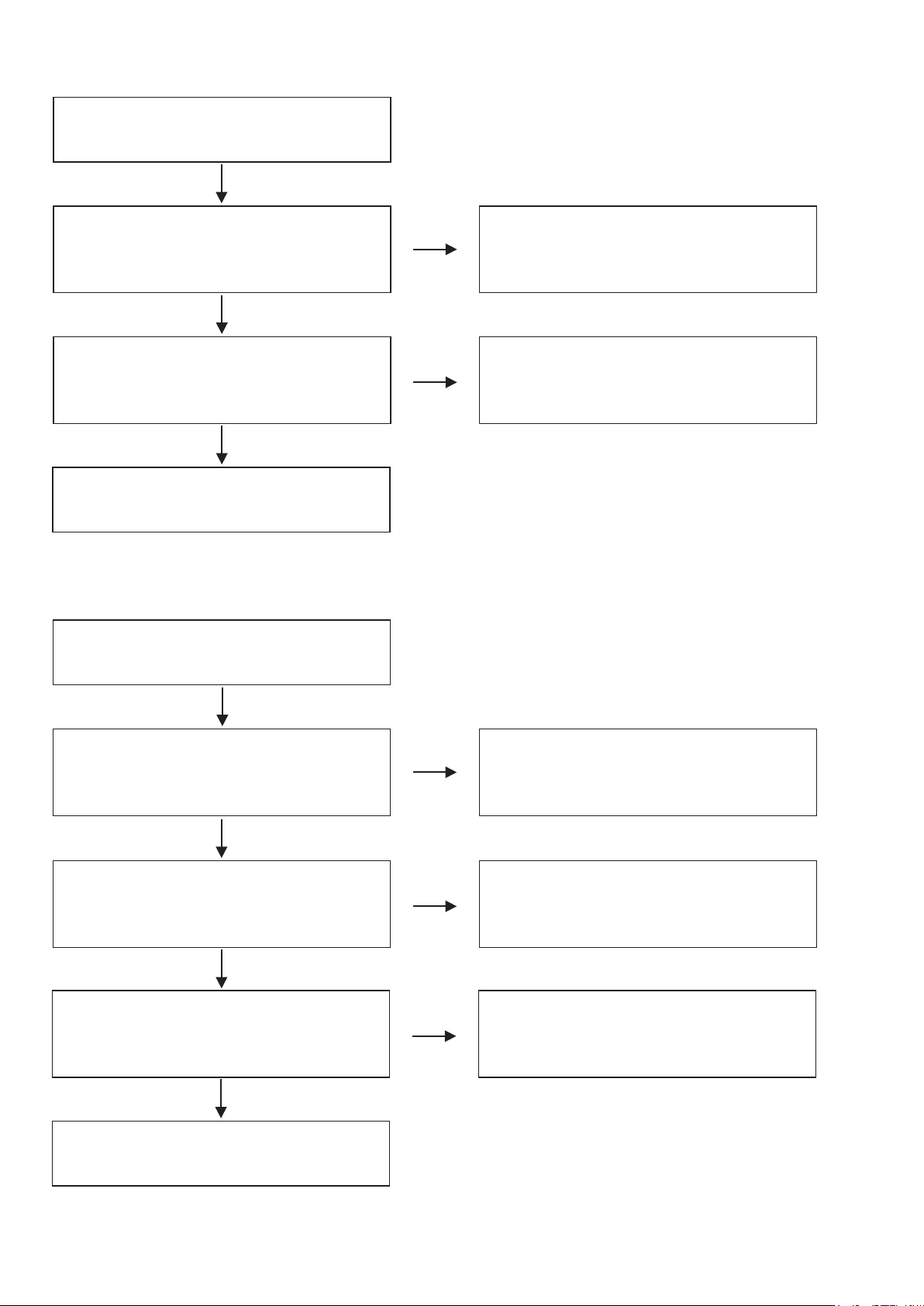
FLOW CHART NO.6 (8U-110068:POWER UNIT)
-15VA is not outputted.
O.K.
Is the fuse normal? See FLOW CHART NO.2 <The fuse blows out.>
O.K.
Is the voltage of -15V or less supplied to IN terminal
of IC906?
O.K.
Check IC906 and the periphery circuit, and replace
it if defective.
FLOW CHART NO.7 (8U-310012:MAIN UNIT, 8U-110068:POWER UNIT)
The VFD display does not light up.
N.G.
N.G.
Check D925 and replace it if defective.
O.K.
Is +5V voltage supplied to 1pin of CX071 on
POWER UNIT?
O.K.
Is +3.3V voltage supplied to 3pin of CX071 on
POWER UNIT?
O.K.
Ia signal outputted from FL_CLK,FL_DATA,FL_
CS,FL_RST terminals of IC104 on MAIN UNIT?
O.K.
Replace the VFD display.
N.G.
N.G.
N.G.
Check the +5V line and service it if defective.
Check the +3.3V line and service it if defective.
Replace IC104.
22
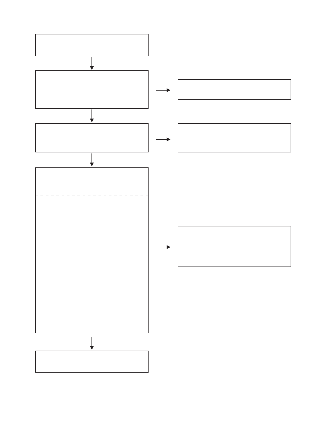
FLOW CHART NO.8 (8U-110069-1:PANEL UNIT)
The key operation is not functioning.
O.K.
Are the contact point and the installation state of
the key switches (S401,S402,S404~S426,S441),
rotary switches (S433~S436), slide switches
(S427,S428,S438,S439), encoder switches (S442
S445) nomal?
~
O.K.
N.G.
Re-install the switches correctly or replace the poor
switch.
Does LED(LD101~LD107, LD109~LD231,
LD401) light correctly ?
O.K.
When pressing each key switches, turning rotary
switches and switching slide switches, do the
voltage of each pin of IC406, IC407(shown below)
increase?
Key switches
S401,404,410,414,418,422 :IC406 11pin
S405,411,415,419,423,425 :IC406 12pin
S426
S402,406,408,412,416,420 :IC406 5pin
S407,409,413,417,421,424,441 :IC406 6pin
Rotary switches
S433,434,435,436 :IC406 11pin
S433,434,435,436 :IC406 12pin
S433,434,435,436 :IC406 13pin
S433,434,435,436 :IC406 14pin
S433,434,435,436 :IC406 3pin
S433,434,435,436 :IC406 4pin
Slide switches
S427,428,438,439 :IC406 5pin
S427,428,438,439 :IC406 6pin
Encoder switches(pressing)
S442 :IC406 5pin
S443 :IC406 6pin
S444 :IC407 11pin
S445 :IC407 12pin
Encoder switches(turning)
S442,443,444,445
IC406 14pin
:
IC407 3,4,13,14pin
:
N.G.
N.G.
Check the TR101~TR116 and their periphery, and
service it if detective.
Check the key switches (S401,S402,S404
S426,S441), and rotary switches (S433~S436),
slide switches (S427,S428,S438,S439), encoder
switches (S442~S445) and their periphery, and
service it if detective.
~
Replace IC406 or IC407.
O.K.
23
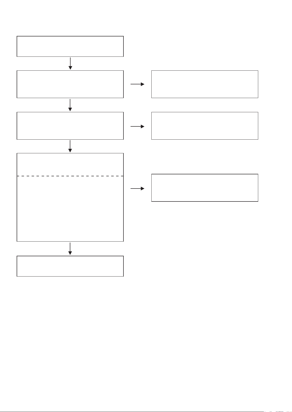
FLOW CHART NO.9 (8U-110070-1:EFECT UNIT)
The key operation is not functioning.
O.K.
Are the contact point and the installation state of
the key switches (S601~S611, S613) normal?
O.K.
Does LED (LD601~LD616) light correctly?
O.K.
When pressing each key switches, pressing and
turning encoder switches, do the voltage of each pin
of IC406, IC407on the 8U-110069-1 board (shown
below) increase?
Key switches
S605,609
S601,606,610 :IC406 5pin
S602,611
S603,607
S604,608,613 :IC407 12pin
Encoder switches(pressing)
S614 :IC407 6pin
Encoder switches(turning)
S614 :IC407 5pin
S614 :IC407 6pin
IC406 4pin
:
IC406 6pin
:
IC407 11pin
:
N.G.
N.G.
N.G.
Re-install the switches correctly or replace the poor
switch.
Check the TR114~TR116 and their periphery, and
service it if detective.
Check the key switches (S601~S611,S613) and
encoder switches (S614) and their periphery, and
service it if detective.
O.K.
Replace IC406 or IC407 on the 8U-110069-1 board.
24
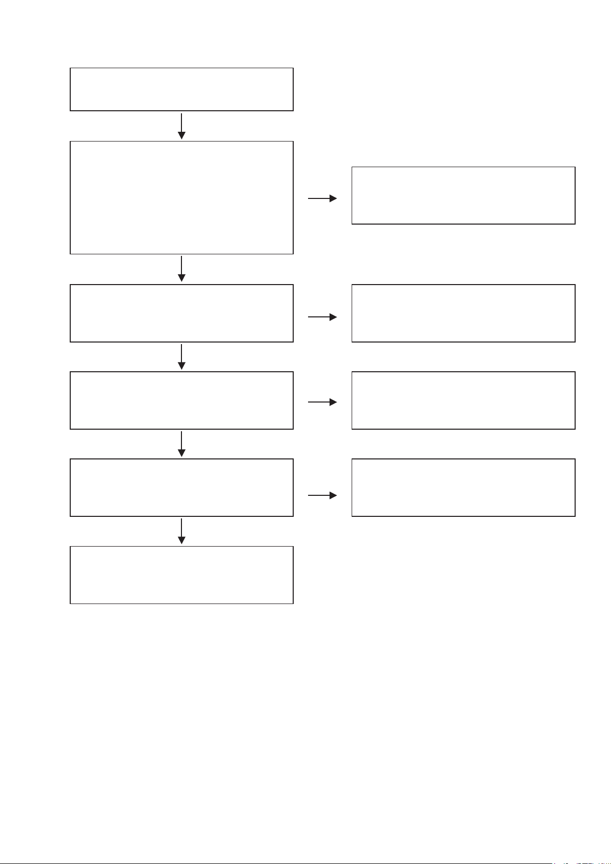
FLOW CHART NO.10 (8U-210093:OUTPUT UNIT)
Function of sound for master output do not operate
normally.
O.K.
Set the line input selector button to "CD".
・
Set the fader assign switch to "THRU".
・
Set the channel fader to "MAX".
・
Set the master level control to "MAX".
・
Are audio signals output to IC101 25pin(left
channel) and 17pin(right channel)when an audio
signal of 1 kHz 0 dBV is input externally to the CD
input?
However, current output.
O.K.
N.G.
Check the input signal from CY232 to IC101 and
their periphery, and service it if detective.
When the input signal is correct, IC101 is replaced.
Are the audio signals outputted to 7pin and 1pin
of IC103(Lch), IC104(Rch), IC105(Lch) and
IC106(Rch)?
O.K.
Are the audio signals outputted to 7pin(COLD) and
1pin(HOT) of IC107(Lch), IC109(Rch)?
O.K.
Is 20pin of CY232 (MUTE control signal)H, and has
been the TR104 collector (MUTE drive signal)
L(-15V)?
O.K.
Check periphery circuit of JK101,JK102 from 7pin
and 1pin of IC107,IC109, and replace it if defective.
N.G.
N.G.
N.G.
Check periphery circuit of IC103,IC104,IC105,IC106
from 25pin、17pin of IC101, and service it if
defective. When the periphery circuit is correct,
IC103,IC104 or IC105,IC106 is replaced.
Check periphery circuit of IC107,IC109 from 7pin
and 1pin of IC105,IC106, and service it if defective.
When the periphery circuit is correct, IC107or
IC109 is replaced.
Check TR111~TR114 and the periphery circuit,
and service it if defective.
25
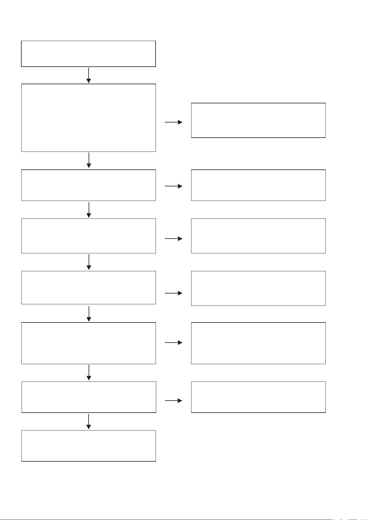
FLOW CHART NO.11 (8U-210092:INPUT UNIT)
Function of sound for master output do not operate
normally.
O.K.
Set the line input selector button to "CD".
・
Set the fader assign switch to "THRU".
・
Set the channel fader to "MAX".
・
Set the master level control to "MAX".
・
Are audio signals output to IC102 7pin(left channel),
1pin(right channel)when an audio signal of 1 kHz 0
dBV is input externally to the CD input?
O.K.
N.G.
Check the input signal from JK101 to IC108 and
their periphery, and service it if detective.
When the input signal is correct, IC108 is replaced.
Is 2pin of CY231 (RELAY control signal)L, and has
been the TR109 collector (RELAY signal) H(+5V)?
O.K.
Are the audio signals outputted to 5pin(Lch) and
6pin(Rch) of RL101?
O.K.
Are the audio signals outputted to 7pin and 1pin of
IC103(Lch), IC104(Rch)?
O.K.
Are the digital audio signals(0-3.3V) outputted from
15pin(DATA) of IC105(L/Rch)?
N.G.
N.G.
N.G.
N.G.
Check TR109 and the periphery circuit, and service
it if defective.
Check periphery circuit of RL101 from IC108, and
service it if defective.
When the input signal is correct, RL101 is replaced.
Check periphery circuit of IC103,IC104 from 5pin
and 6pin of RL101, and service it if defective.
When the input signal is correct, IC103,IC104 is
replaced.
Check that IC105 9pin is "L" (with Fs: 44.1 k/ 48
k),"H" (with Fs: 96 k) and that 19pin is "H". Check
the signal input to 16pin, 17pin and 18pin.
If there is no input signal, repair the defective part.
When the input signal is correct, IC105 is replaced.
O.K.
Are the digital audio signals outputted from 3pin of
IC206?
O.K.
Check periphery circuit of 12pin of CY231 from
3pin of IC206, and replace it if defective.
N.G.
26
Check IC206 and the periphery circuit, and service
it if defective.
When the input signal is correct, IC206 is replaced.
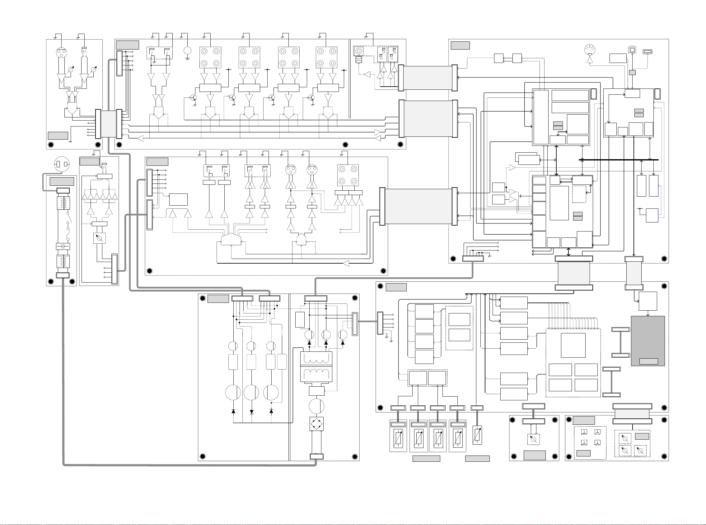
DNX1600 BLOCK DIAGRAM
BLOCK DIAGRAM
MIC1 MIC2
PCM1804
8U-210093-2
MIC UNIT
AC INLET
8U-110068-1
AC INPUT UNIT
2pin VH
HA HA
Diff
ADC
+3.3V
+5VA
+15V
-15V
S.DGND
8U-110070-2
HP UNIT
CX181 CY181
TR
CX021
TR
CX022
2pin VH
MUTE
+15V
-15V
MUTE
18pin FFC P1.0 Si
PHONES
MUTE
CY102
8U-210092
INPUT UNIT
12pin EH
CX121
18pin FFC P1.0 Si
10P-KR
+15V
-15V
+5VA
RL_5V
+3.3V
EFFECT RETURN
L(MONO) R
S.AGND
Diff
ADC
8U-210093-1
OUTPUT UNIT
CX101
10pin EH
10P-SAN
CW102
+15V
-15V
+5VA
RL_5V
+3.3V
CD1 CD2 CD PHONO CD PHONO CD PHONO
GND(PHONO)
MUTE(TR)
MUTE
Cirkit
LINE1 LINE2 LINE3 LINE4
RL_5V
ST
ST
ST
Relay Relay Relay Relay
ST
RL_GND RL_GND RL_GND RL_GND
Diff
PCM1804 PCM1804 PCM1804 PCM1804PCM1804
ADC
EFFECT SEND
L R
TR
MUTEMUTE
Diff
8U-110068-2
POWER UNIT
CW101
DAC
4ST
+15V
PCM1690
24bit
10P-SCN
REG
Diff
RL_5V RL_5V
RIAA
ST
ST
ADC
BOOTH
L R
MUTE MUTE
Σ+LPFΣ+LPFΣ+LPFΣ+LPFΣ+LPFΣ+LPF
REC_Lch
REC_Rch
12P-SCN
REG
-15V
BTLBTL
LDO
+5VA
ST
RIAA
ST
ST
Diff
ADC
MASTER
L
BTL BTL
MUTE MUTE
Σ+LPF Σ+LPF
I-V I-V
Diff
DAC
PCM1795
CW121
1.2V DCDC
RL_5V
ST
ST
Diff
ADC
R
32bit
DA CTL
DA Signal DATA
MCLK/BCK/LRCK for DA
8pin PH
CX081
+5V
+3.3V
AC-DC
RL_5V
RIAA
ST
Relay
AD CTL
AD Signal DATA
MCLK/BCK/LRCK for ADC
MASTER REC
TR
MUTE MUTE
REC_Lch
REC_Rch
+34V
Feed Back
DIGITAL OUT
FADER ST
1 2
CY232
CX071 CW071
7pin KR
3 4
Fader
13pin FFC P1.0 Si
SPDIF
CY131 CX131
23pin FFC P1.0 Si
CY231
23pin FFC P1.0 Si
8U-110069-1
PANEL UNIT
8-1
CW045
Multiplexer
Multiplexer
Multiplexer
Multiplexer
2-1
Multiplexer
(TC4051)
8-1
(TC4051)
8-1
(TC4051)
8-1
(TC4051)
TC4053
+5V
+3.3V
+34V
+1.2V
7pin DA
FLGND
LEDGND
CW046
Multiplexer
CW043
2-1
8U-310012
MAIN UINT
Fader
13pin FFC P1.0 Si
ADC DATA
LRCK/BCK
ADMCLK
23pin FFC P1.0 Si
CX231
LRCK/BCK
23pin FFC P1.0 Si
DAMCLK
CX232
CY081
VR x 10
VR(C) x 17
CW042 CX044
MIDI OUT USB B
DATA
SRCDIT
LRCK/BCK
USB Audio I2S
DGND
16.9344M
24.576
MHz
CS
CS
24
24
3
3
710LRCK/BCK
AHCLK
OUTD1-4
DAC DATA
Hz
OUTD1-4
ADC DATA
710LRCK/BCK
ADC_DAC LRCK/BCK
+5V
+1.2V
+3.3V
3
3-8 DEC
SN74HCT138APW
3
3-8 DEC
SN74HCT138APW
S/P
DRIVER
TB62777FNG
S/P
DRIVER
TB62777FNG
P/S Buffer
SN74LV165APW
P/S Buffer
SN74LV165APW
16MBx16bit
16MBx16bit
SDRAM
SDRAM
DIT
ADDA
MUTE/RST
ADDA CTL
McASP
0
DIR
IF
SRC
IF
DIT
IF
CLK
SEL
LINE
SEL
ADDA
LRCK
BCK
8
8
8
8
8
8
MIX/VR/EQ ect...
DJ EFX
DSP
DA710
+3.3V
+1.2V
EMIF
RST
MCLK
EMIF
32bit
24bit
FIFO REG
CPU IF
(REG_CS2)
FPGA Spartan3A (XC3S400A)
LED/SW
ADDA
MTX
CTL
25pin FFC P1.0 Si8pin PH
CX252
25pin FFC P1.0 Si
CY252
LED x 147
TACT SW x 38
SLIDE SW x 4
AUTO
BPM
UHPI
FFT
4,000LE
+3.3V
+1.2V
SSI-DSP
Buffer
TDM-I2S
SELECTOR x 4
ENC x 5
32bit
UHPI
16bit
14pin
MCLK 16.9344M
4ch TDM
CW082
EHR-44P-SAN4P-SAN 4P-SAN 4P-SAN
48MHz
CPU(USB)
DMA
SH7263
SSI
0/1
ADC
32bit
MAIN BUS
RST(soft)
x2
CX072
CY072
CZ041
4pin DA
4pin DA
CW041
CZ031
3pin DA
3pin DA
CW031
23pin FFC P1.0 Si8pin KR
USB SW
USB CTL
+3.3V
CPU
+1.2V
VFD_IF
32bit 16bit
7pin FFC P1.0 Si
7pin FFC P1.0 Si
BN061GINK
USB A
14pin
RST
Audio CLK
BUS
I/O
32bit
SDRAM
8MBx32bit
1MB F-ROM
+5V
RST
VFD
Cirkit
VFD
CX233
2pin VH
CY022
27
PHR-4 PHR-4 PHR-4 PHR-4
CH FADER
X-FADER
8pin DS
CY082
8U-110069-2
SPLIT UNIT
8U-110070-1
EFFECT UNIT
FUNC1 FUNC2
FUNC3 FUNC4
MIDI
23pin FFC P1.0 Si
CY233
EFX
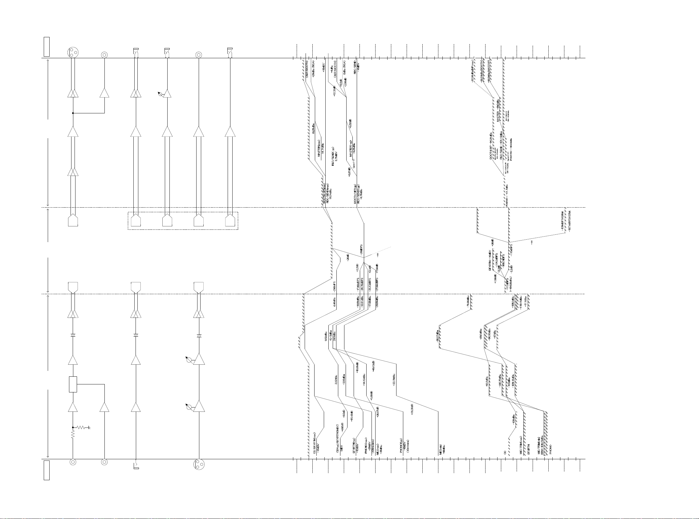
LEVEL DIAGRAM
+30
(XLR)
+4dBu(typ)
MASTER OUT
BTL
+6.0dB
0dB
Σ
SUM
I-V
Rf=1.5kohm
(RCA)
+0dBu(typ)
MASTER OUT
+2.59dB
PAD+AMP
(-3.41+6.0)
+4dBu(typ)
BOOTH OUT
BTL
+6.0dB
Σ
SUM
+6.87dB
HP OUT
VR
-∞~+12dB
SUM
+6.87dB
REC OUT
150mW@40hom
Σ
-10dBV(typ)
0dB
Σ
SUM
EFX SEND
-10dBV(typ)
0dB
Σ
SUM
[dBu]
+30
[dBV]
+20
+10
+24dBu
BTL
VOE=±13.5V=+21.81dBu
Diff
Clip Level
0
-10
-20
-30
-40
-50
-60
-70
-80
-90
-100
-110
-120
0
-10
-20
-30
-40
-50
-60
-70
-80
-90
-100
-110
+10dBu (HP)
-120
-130
-130
-140
-140
-150
-150
DAC
32bit
PCM1795
ADC
PCM1804
PAD
-20.06dB
+
+2.5V
Offset
Diff
+6.0dB
Analog AnalogDigital
RELAY
DAC
PCM1690
ADC
PCM1804
PAD
-20.06dB
+
+2.5V
Offset
Diff
+6.0dB
DAC
DAC
ADC
PCM1804
PAD
-20.06dB
+
+2.5V
Offset
DAC
0dBFS
(+7.14dBu)
Clip Level
[dBFS] [dBFS]
Vcom=+2.5Voffset
Diff
※ 22Hz-20kHz(SPCL), A-Weighted, FS96kHz
Typical Noise Level ※ Typical Noise Level ※
Amp
+6.0dB
PAD
-4.62dB
INPUT OUTPUT
CD1~4
0dBV(typ)
RIAA
+36.07dB
10mV(typ)
PHONO1~4
Amp
+6.0dB
0dBV(typ)
EFX RETURN
HA HA
1st 2nd
+6.0dB~+26.5dB +18.0dB~+40.0dB
Diff
MIC
-60~-20dBu
VOE=±13.5V=+21.81dBu
Clip Level
+30
+30
+20
+20
[dBV]
[dBu]
+10
+10
0
-10
-20
-30
-40
-50
-60
-70
-80
-90
-100
-110
-120
-130
-140
0
-10
-20
-30
-40
-50
-60
-70
-80
-90
-100
-110
-120
-130
-140
-150
-150
28
2
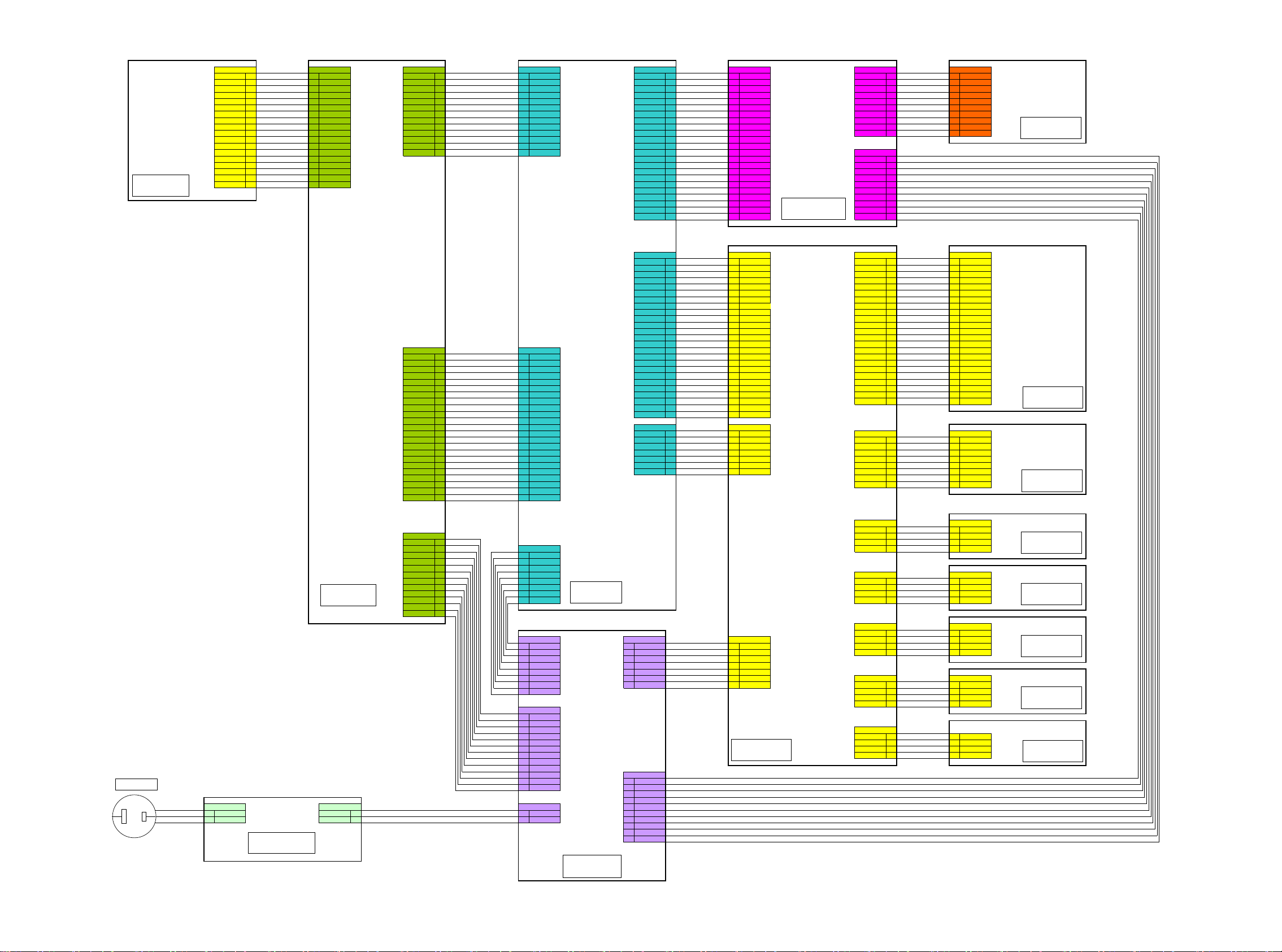
DNX1600 WIRING DIAGRAM
WIRING DIAGRAM
MIC UNIT
8U-210093-2
CX181 CY181 CY131 CX131 CX232 CY232 CW102 CY102
S.DGND 1 1 S.DGND GND 1 1 GND GND 1 1 GND HP_L 1 1 HP_L
A_RST 2 2 A_RST CUE1 2 2 CUE1 A_RST 2 2 A_RST AG_L 2 2 AG_L
AD_ORS0 3 3 AD_ORSD PLAY1 3 3 PLAY1 DA_SCK 3 3 DA_SCK AG_R 3 3 AG_R
ADLRCK 4 4 ADLRCK CUE2 4 4 CUE2 DA_TX 4 4 DA_TX HP_R 4 4 HP_R
ADBCK 5 5 ADBCK PLAY2 5 5 PLAY2 DA_CS1 5 5 DA_CS1 GND 5 5 GND
S.DGND 6 6 S.DGND GND 6 6 GND DA_CS2 6 6 DA_CS2 +15V 6 6 +15V
MICDAT 7 7 MICDAT CUE3 7 7 CUE3 NC 7 7 -15V 7 7 -15V
S.DGND 8 8 S.DGND PLAY3 8 8 PLAY3 GND 8 8 GND RL_MUTE 8 8
ADMCLK 9 9 ADMCLK CUE4 9 9 CUE4 DALRCK 9 9 DALRCK 9 9
S.DGND 10 10 S.DGND PLAY4 10 10 PLAY4 DABCK 10 10 DABCK 10 10
S.AGND 11 11 S.AGND GND 11 11 GND MASTDAT 11 11 MASTDAT
+15V 12 12 +15V SPDIF 12 12 SPDIF BOOTDAT 12 12 BOOTDAT
S.AGND 13 13 S.AGND GND 13 13 GND GND 13 13 GND
-15V 14 14 -15V RECDAT 14 14 RECDAT +15V 1
+5VA 15 15 +5VA PHONDAT 15 15 PHONDAT AGND 2
S.AGND 16 16 S.AGND EFXSDAT 16 16 EFXSDAT AGND 3
+3.3V 17 17 +3.3V GND 17 17 GND -15V 4
S.DGND 18 18 S.DGND SND_DET_L 18 18 RE_5V 5
CY231 CX231
GND 1 1 GND GND 16 16 DGND SD6 16 16 SD6
RELAY1 2 2 RELAY1 BLINK 17 17 BLINK SD5 17 17 SD5
RELAY2 3 3 RELAY2 SCK 18 18 SCK SD8 18 18 SD8
RELAY3 4 4 RELAY3 LEDDAT 19 19 LEDDAT SD7 19 19 SD7
RELAY4 5 5 RELAY4 SD0 20 20 SD0 SD14 20 20 SD14
GND 6 6 GND SD1 21 21 SD1 SD9 21 21 SD9
A_RST 7 7 A_RST LCD_BLL 22 22 LCD_BLL SD15 22 22 SD15
AD_OSR0 8 8 AD_OSR0 GND 23 23 DGND DGND 23 23 DGND
ADLRCK 9 9 ADLRCK LCD_RLH 24 24 LCD_BLH
ADBCK 10 10 ADBCK GND 25 25 DGND
GND 11 11 GND
ADDAT1 12 12 ADDAT1
ADDAT2 13 13 ADDAT2 D.GND 1 1 FL_DGND
ADDAT3 14 14 ADDAT3 LCD_B0 2 2 FL_CLK SL0 1 1 SL0
ADDAT4 15 15 ADDAT4 LCD_B1 3 3 FL_GND LD7 2 2 LD7
GND 16 16 GND LCD_B2 4 4 FL_DATA DGND 3 3 DGND
EFXRDAT 17 17 EFXRDAT LCD_B3 5 5 FL_CS SD7 4 4 SD7
MICDAT 18 18 MICDAT LCD_B4 6 6 FL_RST DGND 5 5 DGND
RTN_DET_L 19 19 RTN_DET_L D.GND 7 7 FL_DGND VR1-3 6 6 VR1-3
RTN_DET_R 20 20 RTN_DET_R DGND 7 7 DGND
GND 21 21 GND +3.3V 8 8 +3.3V
ADMCLK 22 22 ADMCLK
GND 23 23 GND
NC 19 19 RE_GND 6
RE_MUTE 20 20 RE_MUTE +5VA 7
GND 21 21 GND AGND 8
DAMCLK 22
GND 23 23 GND DGND 10
CX252 CY252 CX233 CY233
GND 1 1 DGND ADJVOL 1 1 ADJVOL
VR_DAT1 2 2 VR_DAT1 DRY/WETV 2 2 DRY/WETV
VR_DAT2 3 3 VR_DAT2 DGND 3 3 DGND
VR_DAT3 4 4 VR_DAT3 +3.3V 4 4 +3.3V
VR_DAT4 5 5 VR_DAT4 SL13 5 5 SL13
GND 6 6 DGND SL14 6 6 SL14
GND 7 7 DGND SL15 7 7 SL15
FADER_DAT
GND 9 9 DGND LD11 9 9 LD11
XFADER 10 10 XFADER LD12 10 10 LD12
GND 11 11 DGND LD13 11 11 LD13
SC0 12 12 SC0 LD14 12 12 LD14
SC1 13 13 SC1 LD15 13 13 LD15
SC2 14 14 SC2 LD8 14 14 LD8
SC3 15 15 SC3
8 8 FADER_DAT2 AGND 8 8 AGND
CX072 CY072
22 DAMCLK +3V3 9
OUTPUT UNIT
8U-210093-1
CX101
DGND 15
CW082 CY082
MUTE
15 DGND
HP UNIT
8U-110070-2
EFFECT UNIT
8U-110070-1
SPLIT UNIT
8U-110069-2
AC INLET
CX121
+15V 1 NC 3 3 NC
+15V 2
P.AGND 3 8 PFAIL
P.AGND 4 7 +1.2V
-15V 5 6 +1.2V
-15V 6
RL_5V 7 4 +3.3V +3.3V 1 1 +3.3V
INPUT UNIT
8U-210092
CX021 CX022 CY022
1 HOT COLD 1 1 COLD 5 RE_5V
2 COLD HOT 2 2 HOT 4 -15V
RL_GND 8 3 DGND PITCH 2 2 PITCH
+5VA 9 2 +5VD NC 3 3 NC
P.AGND. 10 1 +5VD DGND 4 4 DGND
+3V3 11
P.DGND 12
POWER SW
CY081
5 DGND
MAIN UNIT
8U-310012A
CX081 CX071 CW071
1 +5VD 1 +5VD 1 +5V NC 3 3 NC
2 +5VD 2 DGND 2 AGND DGND 4 4 DGND
3 GND 3 +3V3 3 +3.3V
4 +3V3 4 DGND 4 AGND
5 DGND 5 +34V 5 34V
6 +1V2 6 DGND 6 FL_GND
7 +1V2 7 +1V2 7 +1.2V +3.3V 1 1 +3.3V
8 PFAIL PITCH 2 2 PITCH
CW121
1 +15V
2 +15V
3 AGND
4 AGND +3.3V
5 -15V DGND 2 2 DGND
6 -15V NC 3 3 NC
7 RE_5V +3.3V 4 4 +3.3V
8 RE_GND
9 +5VA
10 AGND
11 +3V3 10 DGND
12 DGND 9 +3V3
CW101
8 AGND
7 +5VA
6 RE_GND
3 AGND
2 AGND
1 +15V
UNIT
POWER UNIT
8U-110068-2
PANEL1 UNIT
8U-110069-1
CW046 CX046
+3.3V 1 1 +3.3V
PITCH 2 2 PITCH
DGND 4 4 DGND
CW045 CX045
CW043 CX043
+3.3V 1 1 +3.3V
PITCH 2 2 PITCH
CW042 CX042
NC 3 3 NC
DGND 4 4 DGND
CX044
1 1 +3.3V
FEDER UNIT
8U-110070-3
FEDER UNIT
8U-110069-4
FEDER UNIT
8U-110069-5
FEDER UNIT
8U-110069-6
CROSS
FADER
29
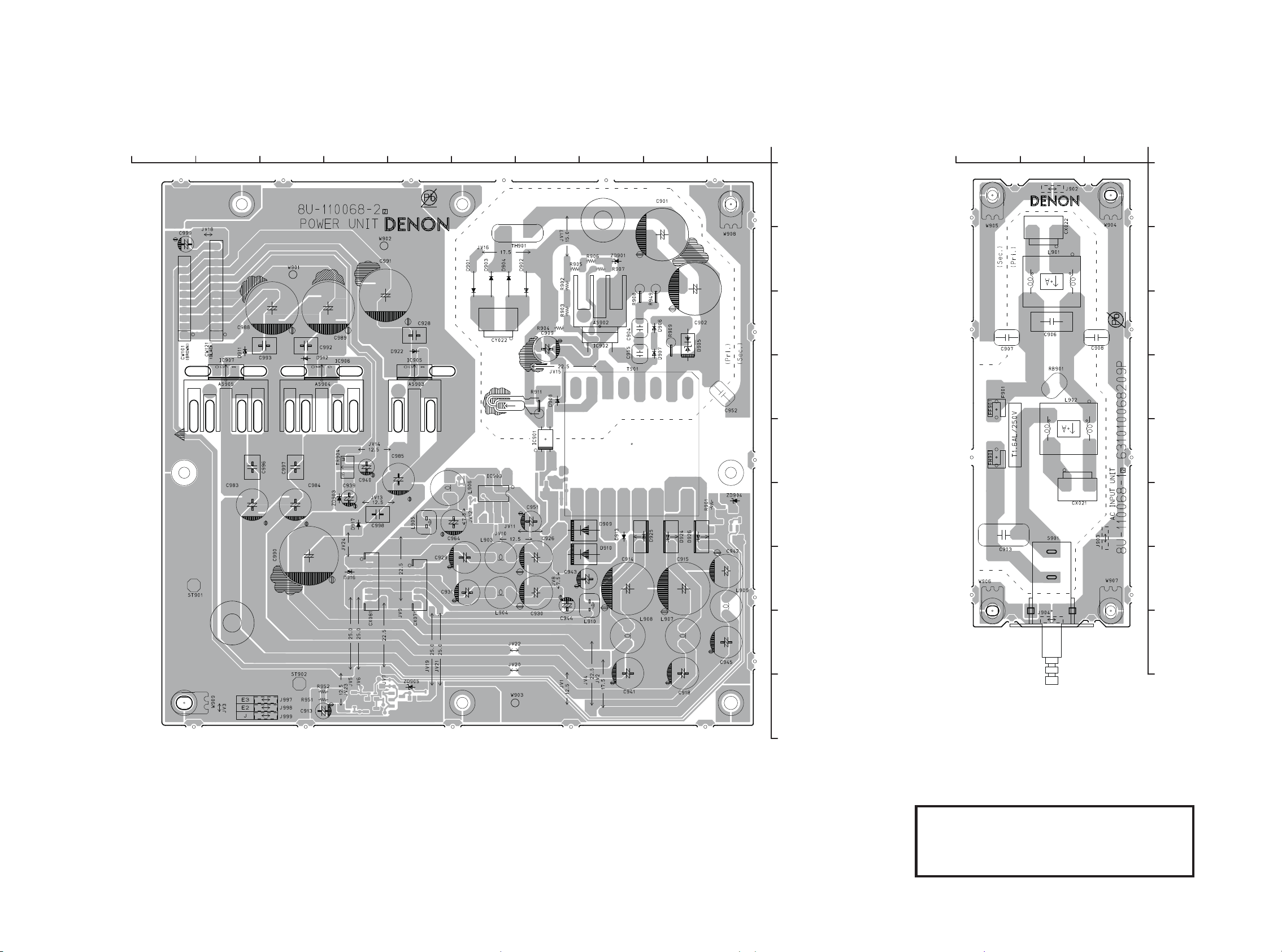
PRINTED WIRING BOARDS
8U-110068-2 (COMPONENT SIDE) 8U-110068-1 (COMPONENT SIDE)
1817161514131211109
321
A
C
F
B
D
A
B
C
D
E
E
F
G
H
I
G
H
鉛フリー半田
半田付けには、鉛フリー半田 (Sn-Ag-Cu) を使用してください。
Lead-free Solder
When soldering, use the Lead-free Solder (Sn-Ag-Cu).
30
 Loading...