

Ver. 1
SERVICE MANUAL
MODEL JP E3 E2 EK E2A E2C E1K EUT
DN-X1100
33
DJ MIXER
●
For purposes of improvement, specifications and design are subject to change without notice.
●
Please use this service manual with referring to the operating instructions without fail.
●
Some illustrations using in this service manual are slightly different from the actual set.
PROFESSIONAL BUSINESS COMPANY
X0409 V.01 DE/CDM 0901
SAFETY PRECAUTIONS
The following check should be performed for the continued protection of the customer and service technician.
LEAKAGE CURRENT CHECK
Before returning the unit to the customer, make sure you make either (1) a leakage current check or (2) a line to chassis
resistance check. If the leakage current exceeds 0.5 milliamps, or if the resistance from chassis to either side of the
power cord is less than 460 kohms, the unit is defective.
CAUTION
Please heed the points listed below during servicing and inspection.
◎ Heed the cautions!
Spots requiring particular attention when servicing, such
as the cabinet, parts, chassis, etc., have cautions indicated
on labels or seals. Be sure to heed these cautions and the
cautions indicated in the handling instructions.
◎ Caution concerning electric shock!
(1) An AC voltage is impressed on this set, so touching in-
ternal metal parts when the set is energized could
cause electric shock. Take care to avoid electric shock,
by for example using an isolating transformer and
gloves when servicing while the set is energized, unplugging the power cord when replacing parts, etc.
(2)There are high voltage parts inside. Handle with extra
care when the set is energized.
◎ Caution concerning disassembly and
assembly!
Though great care is taken when manufacturing parts from
sheet metal, there may in some rare cases be burrs on the
edges of parts which could cause injury if fingers are
moved across them. Use gloves to protect your hands.
◎ Inspect for safety after servicing!
Check that all screws, parts and wires removed or disconnected for servicing have been put back in their original positions, inspect that no parts around the area that has been
serviced have been negatively affected, conduct an insulation check on the external metal connectors and between
the blades of the power plug, and otherwise check that
safety is ensured.
(Insulation check procedure)
Unplug the power cord from the power outlet, disconnect
the antenna, plugs, etc., and turn the power switch on. Using a 500V insulation resistance tester, check that the insulation resistance between the terminals of the power
plug and the externally exposed metal parts (antenna terminal, headphones terminal, microphone terminal, input
terminal, etc.) is 1MΩ or greater. If it is less, the set must
be inspected and repaired.
CAUTION
Concerning important safety
parts
◎ Only use designated parts!
The set's parts have specific safety properties (fire resistance, voltage resistance, etc.). For replacement parts, be
sure to use parts which have the same properties. In particular, for the important safety parts that are marked z on
wiring diagrams and parts lists, be sure to use the designated parts.
◎ Be sure to mount parts and arrange
the wires as they were originally!
For safety reasons, some parts use tape, tubes or other insulating materials, and some parts are mounted away from
the surface of printed circuit boards. Care is also taken with
the positions of the wires inside and clamps are used to
keep wires away from heating and high voltage parts, so
be sure to set everything back as it was originally.
Many of the electric and structural parts used in the set
have special safety properties. In most cases these properties are difficult to distinguish by sight, and using replacement parts with higher ratings (rated power and
withstand voltage) does not necessarily guarantee that
safety performance will be preserved. Parts with safety
properties are indicated as shown below on the wiring diagrams and parts lists is this service manual. Be sure to replace them with parts with the designated part number.
(1) Schematic diagrams ... Indicated by the z mark.
(2) Parts lists ... Indicated by the z mark.
Using parts other than the designated
parts could result in electric shock, fires or
other dangerous situations.
2
DN-X1100
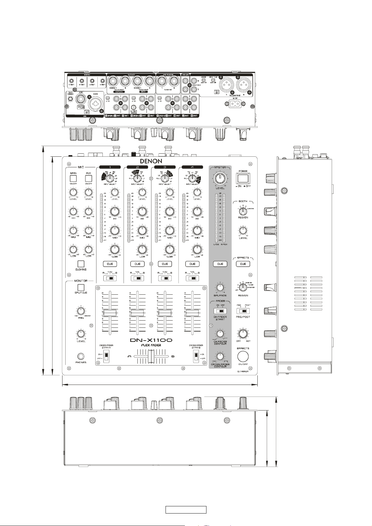
DIMENSION
374mm
357mm
320 mm
114 mm
92.5 mm
3
DN-X1100
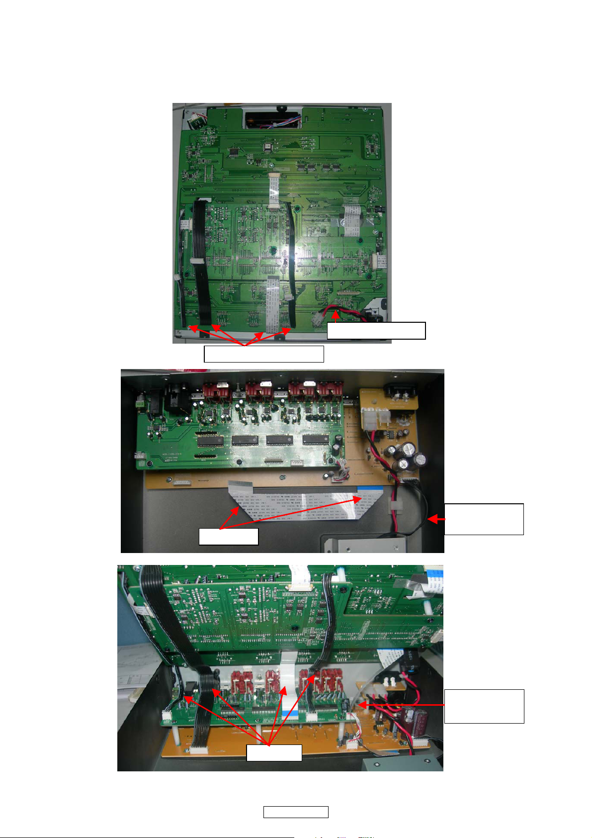
WIRE ARRANGEMENT
If wire bundles are untied or moved to perform adjustment or parts replacement etc., be sure to rearrange them neatly as they
were originally bundled or placed afterward.
Otherwise, incorrect arrangement can be a cause of noise generation.
Flat cable (Broken line)
Broken line
AC Line cable twist
It draws it to the
chassis side
Flat cable
DN-X1100
FFC line left the
AC line
4
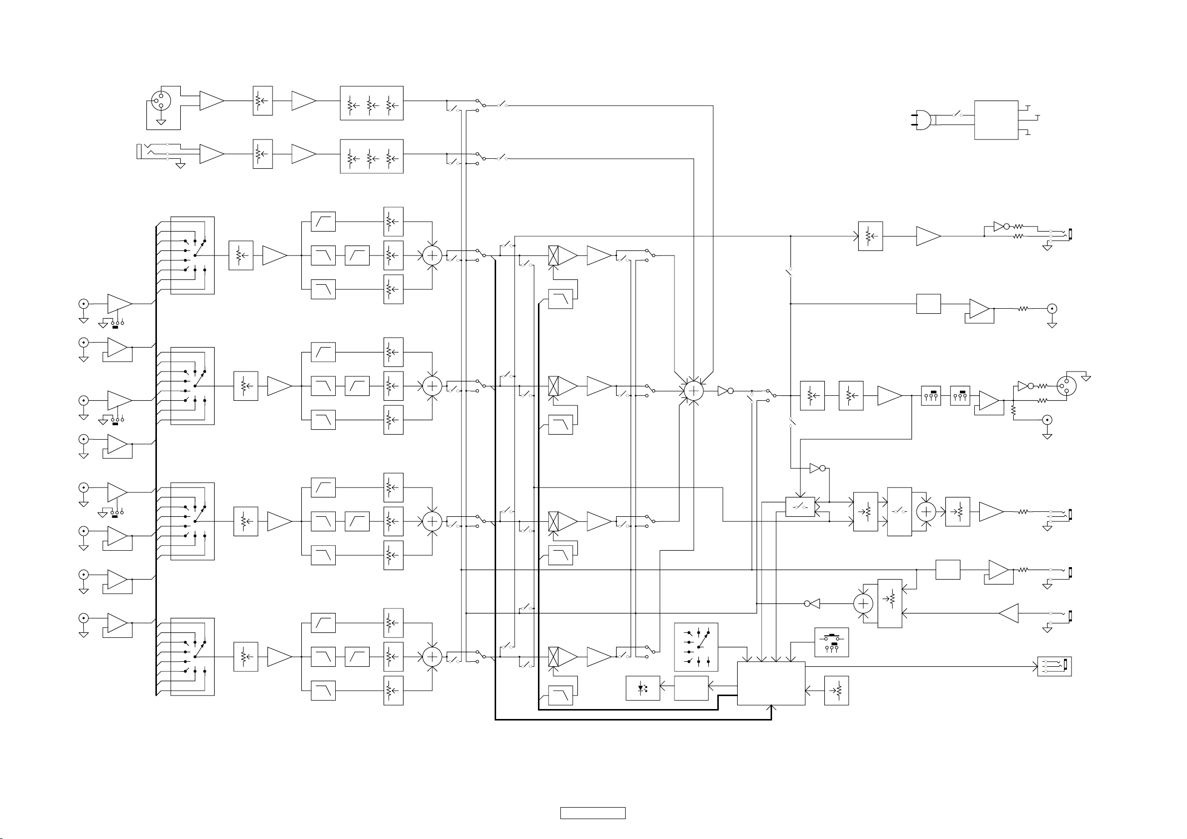
BLOCK DIAGRAM
PH1/LINE1
LINE2
PH2/LINE3
LINE4
AMP
0,36dB
PH LIN E
2C11
BUFFER
AMP
PH LIN E
2
C1
1
BUFFER
MAI N MI C IN
AUX MIC IN
(-14dBV)
(-20dB)
CH1 GAIN
3
1
CH2 GAIN
MAI N MI C L EVEL
31
AUX MIC LEVEL
31
2
31
2
2
2
12dB
AMP
AMP
(-2dBV)
12dB
18.5dB
AMP
AMP
(-2dBV)
(-1.5dBV)
HPF
LPF
LPF
HPF
LPF
LPF
2
H
C
3
G
1
3
4
5
6
3
4
5
6
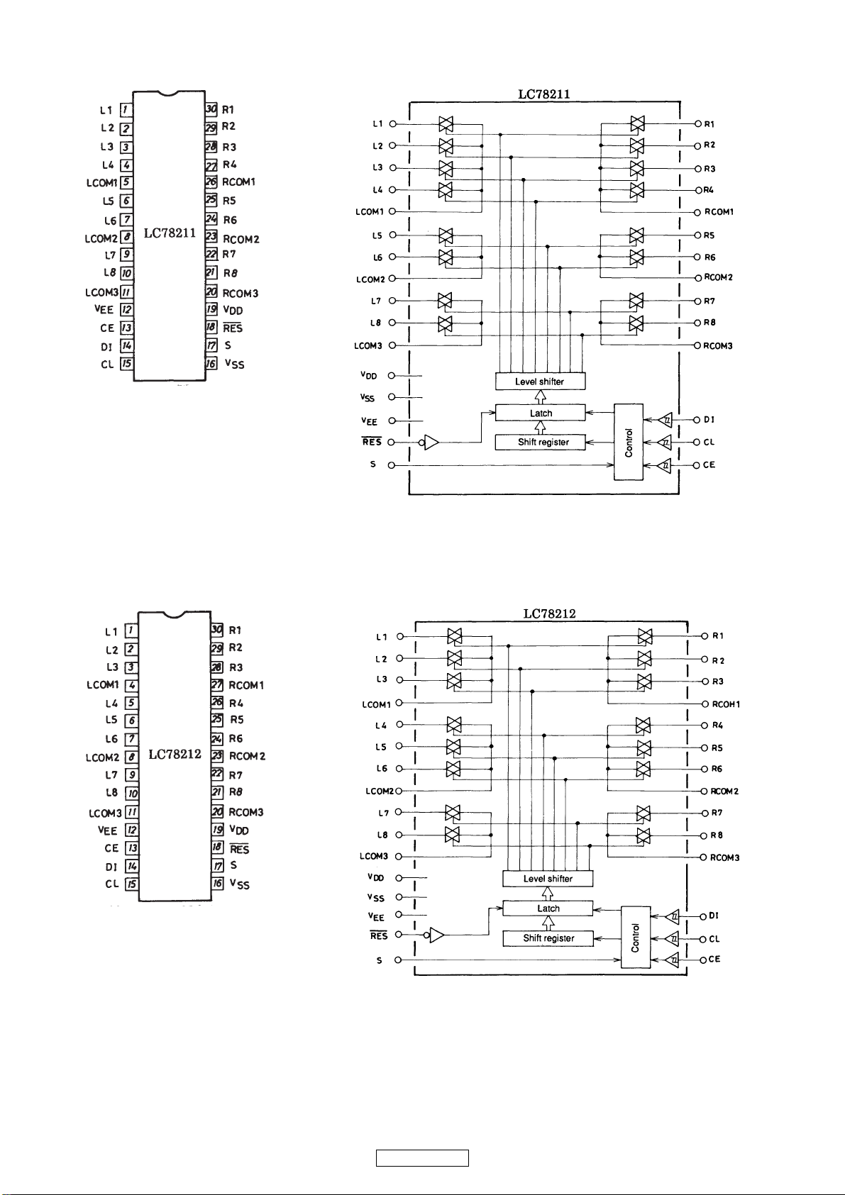
LC78211
LC78211
AMP
40dB
AMP
40dB
2
1
A
C1
7
8
2
1
A
C1
7
8
MAIN MIC EQ
3123
AUX MIC EQ
3123
HPF
HPF
MID
1
1
HILOW MID
2312
HILOW
3
2
1
HI
31
MID
3
1
LOW
3
1
HI
31
MID
3
1
LOW
31
1 2
1 2
(-2dBV)
1 2
1 2
MAIN MIC FX
1
A
2
AUX MIC FX
1
A
2
1
A
2
CH1 PRE FX
1
A
2
CH2 PRE FX
1 2
C1
C1
1 2
BOOTH 1
C1
BOOTH 2
C1
OFF
OFF
1 2
1 2
AMP
4.85dB
ATT.
-6.37dB
MONO/ST
2C11
POWER SW.
1 2
(+2.85dBV)
(-8.17dBV)
ATT - 10dB
2
C1
1
SWITCHING
POWER SUPPLY
BUFFER
BUFFER
ON
ON
BOOTH LEVEL
31
1 2
CUE1
1 2
CUE2
VCA
VCA
(-11.54dBV)
-3dB
LPF
LPF
9.54dB
AMP
AMP
(-1.8dBV)
1 2
(-1.8dBV)
1 2
1
A
C1
2
CH1 POST FX
1
A
C1
2
CH2 POST FX
INV.
(-1.8dBV)
1 2
MASTER FX
1
A
2
C1
BOOTH
MASTER
1 2
(-1.8dBV)
MASTER BAL.
12
CUE MASTER
MASTER L EVEL
31
31
2
2
-3.4dB
AC IN
2
AMP
(+1.73dBV)(-5.2dBV)
6.93dB
INV.
15V
-15V
300
300
1K
INV.
AV=1.74dB
1K
(+0.9dBV)
5V
(5.07dBm)
(-9dBV)
300
300
3
2
1
(4.87dBm)
3
L
BOOTH OUT
R
G
REC OUT
1
G
C
H
MASTER BAL . OUT
2
MASTER OUT
(-2dBV)
2
2
2
2
2
2
2
(-1.5dBV)
/PH3LINE5
LINE6
LINE7
LINE8
AMP
PH LIN E
2
C11
BUFFER
BUFFER
BUFFER
LC78211
3
4
5
6
LC78211
3
4
5
6
INV. AV=3.5dB.
HPF
2
1
A
CH3 GAIN
C1
7
8
2
1
A
C1
8
7
3
1
CH4 GAIN
31
AMP
2
AMP
2
LPF
LPF
HPF
LPF
LPF
HPF
HPF
31
3
1
3
1
3
1
31
3
1
HI
MID
LOW
HI
MID
LOW
2
BOOTH 3
1 2
1
2
2
2
2
2
1 2
1 2
A
2
CH3 PRE FX
1
A
2
CH4 PRE FX
C1
C1
BOOTH 4
1 2
1 2
CUE3
FX CU E
1 2
1 2
CUE4
(+1.5dBV)
VCA
VCA
LPF
SPLIT CUE
AMP
LPF
AMP
I EVEL METERS
(-1.8dBV)
1 2
(-1.8dBV)
1 2
CH4 POST F X
NDCATORS & L
1
A
C1
2
CH3 POST F X
1
A
C1
2
SWITCHES
2
3
4
5
6
7
LED DRIVER
1
A
C1
8
PWM
PFL
L/CUE
1 2
INV.
KEYS & SWITHES
R/PGM
2C11
CPU
(+1.7dBV)
MASTER
CUE
(+1.5dBV)
31
2
CUE PAN
2
FAD ERS & VRS
SPLIT CUE
31
1 2
FX PAN
2
(-2dBV)
31
CUE LEVEL
2
ATT.
-10.39dB
31
(-12.39dBV)
AMP
6dB
(-2dBV)
BUFFER
(+7dBV)
AMP
33
3
(+1dBV)
L
2
1
1K
13.22dBV)
(-
1
3
1
3
2
1
L
R
G
3
R
G
L
G
L
G
PHONES OUT
SEND
RETURN
PLAY CONTROL
5
DN-X1100
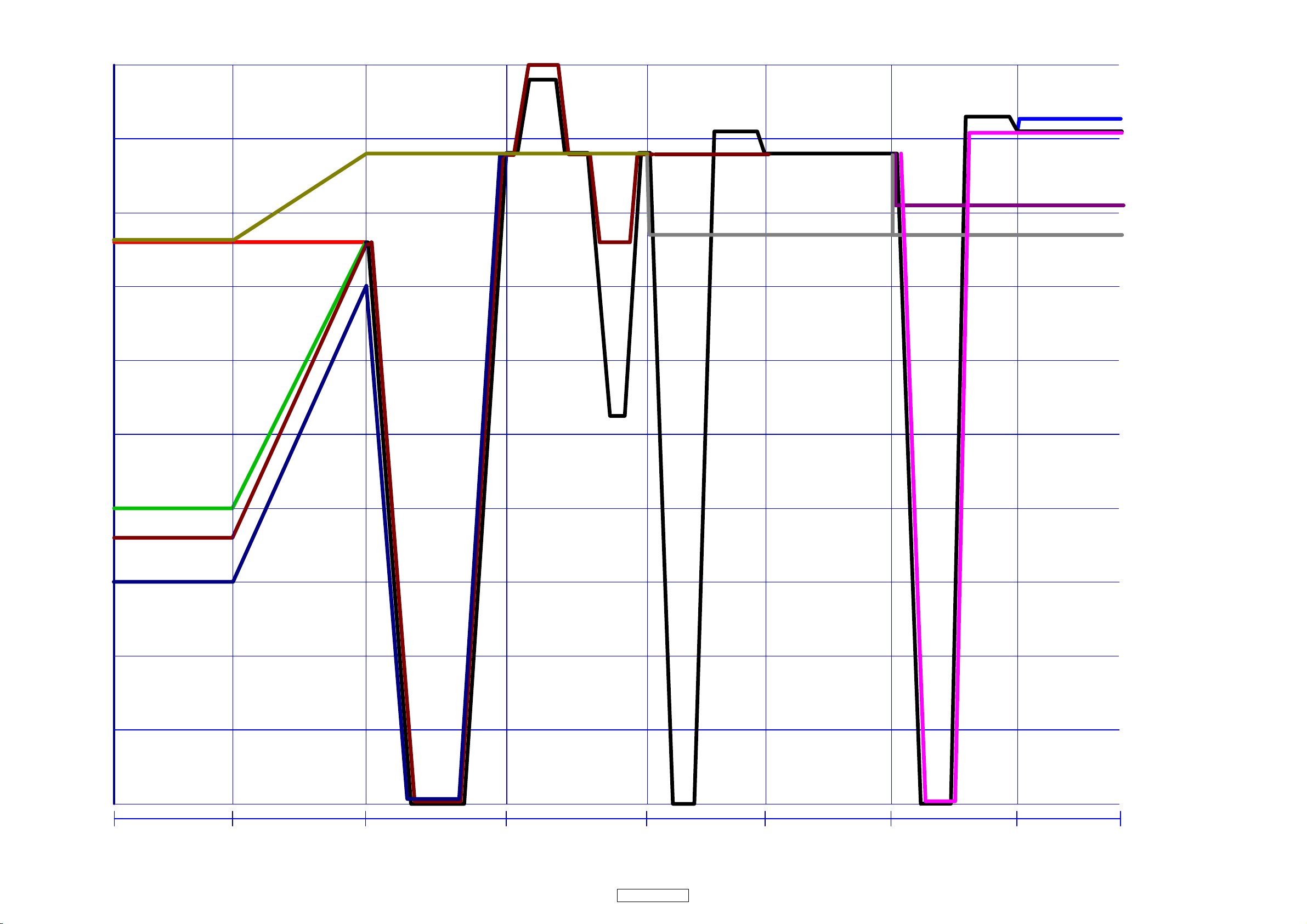
LEVEL DIAGRAM
10dBV
0dBV
BALANCED OUT
UNBALANCED OUT
PHONES OUT
-10dBV
-20dBV
-30dBV
-40dBV
-50dBV
RETURN INPUT
LINE INPUT
PHONO INPUT
REC OUT
SEND OUT
-60dBV
-70dBV
-80dBV
-90dBV
MAIN MIC INPUT
AUX MIC INPUT
INPUT PRE. AMP
MAIN MIC GAIN
AUX MIC GAIN
INPUT GAIN
MIC EQ
CH. EQ
FADER
MIX
CUE LEVEL
MASTER LEVEL
OUTPUT
6
DN-X1100
SEMICONDUCTORS
(
Only major semiconductors are shown, general semiconductors etc. are omitted to list.
The semiconductor which described a detailed drawing in a schematic diagram are omitted to list.
1. IC’s
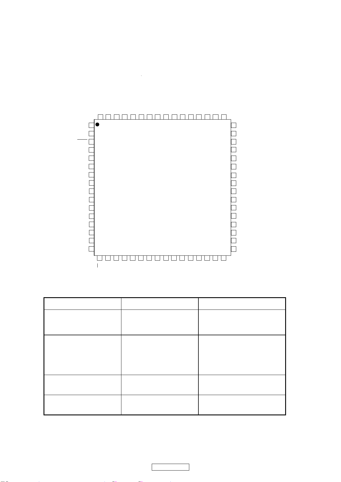
MC9S08AW32CPUE (IC801)
PTC4
IRQ
RESET
PTF0/TPM1CH2
PTF1/TPM1CH3
PTF2/TPM1CH4
PTF3/TPM1CH5
PTF4/TPM2CH0
PTC6
PTF7
PTF5/TPM2CH1
PTF6
PTE0/TxD1
PTE1/RxD1
PTE2/TPM1CH0
PTE3/TPM1CH1
PTC5/RxD2
64
63 62 61
1
2
3
4
5
6
7
8
9
10
11
12
13
14
15
16
18
17
PTE4/SS1
PTC3/TxD2
PTC2/MCLK
19
PTE6/MOSI1
PTE5/MISO1
PTC1/SDA1
20 21 22
PTE7/SPSCK1
PTC0/SCL1
59
60
SS
V
SS
V
58
64-Pin LQFP
23
DD
V
BKGD/MS
PTG6/EXTAL
PTG5/XTAL
56
57
64-Pin QFP
PTG2/KBI1P2
PTG1/KBI1P1
PTG0/KBI1P0
REFH
REFL
V
V
27
26
PTA024PTA125PTA2
PTD5/AD1P13
PTD6/TPM1CLK/AD1P14
PTD7/KBI1P7/AD1P15
28 29 30 31
PTA4
PTA3
PTD4/TPM2CLK/AD1P12
PTG4/KBI1P4
49
505152535455
PTA5
47
46
45
44
43
42
41
40
39
38
37
36
35
34
32
PTA6
PTG3/KBI1P3
48
PTD3/KBI1P6/AD1P11
PTD2/KBI1P5/AD1P10
V
SSAD
V
DDAD
PTD1/AD1P9
PTD0/AD1P8
PTB7/AD1P7
PTB6/AD1P6
PTB5/AD1P5
PTB4/AD1P4
PTB3/AD1P3
PTB2/AD1P2
PTB1/AD1P1
PTB0/AD1P0
PTA7
33
SYMPTOM POSSIBLE CAUSE CORRECTION ACTION
The power fails to switch on
when the POWER switch is set to
on
No output
Poor power plug connection at the
AC outlet
1) Improper outlet cable
connections
2) Improper amplifier operation
3) Improper setup of input cable
Connection and switch
Insert the power plug firmly into the
AC outlet
1) Connect the output cable correctly
2) Check amplifier setup
3) Correct the position of input cable
and switch correctly
Hum Loose cable connections Firmly connect all audio plugs
Line / Phono switch reversed Poor power plug connection Connection the input cable correctly
7
DN-X1100
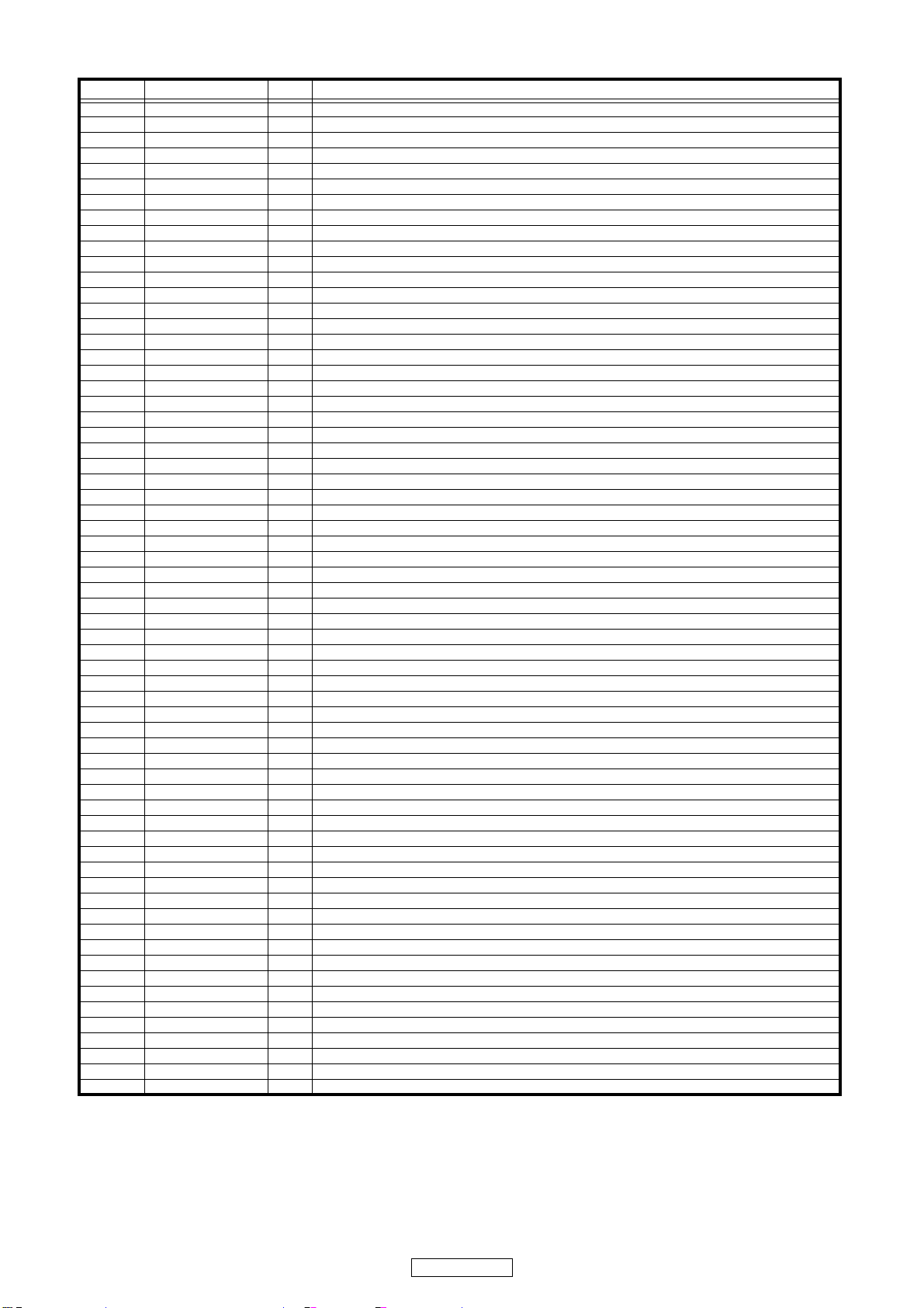
MC9S08AW32CPUE Terminal Function
Pin No. Pin Name I/O I/O Function
1 PC3B' O LINE6 FADER CONTROL OUT
2IRQ
3 RESET
4 PWM1' O CH 1 VCA CONTROL
5 PWM2' O CH 2 VCA CONTROL
6 PWM3' O CH 3 VCA CONTROL
7 PWM4' O CH 4 VCA CONTROL
8 PC4A' O LINE8 FADER CONTROL OUT
9 PC4B' O LINE8 FADER CONTROL OUT
10 JDET I EFFECT SEND/RETURN IN
11 CHFS I CH FADER START SW IN
12 PRE/POST I PRE/POST SW INPUT
13 CFSA/TX I CROSS FADER START A SW IN
14 CFSB/RX I CROSS FADER START B SW IN
15 KFXON I EFFECTS ON IN
16 - 17 CE1 O LC78211,LC78212,LC78213 CONTROL PIN
18 CE2 O LC78211,LC78212,LC78213 CONTROL PIN
19 DI O LC78211,LC78212,LC78213 CONTROL PIN
20 CL O LC78211,LC78212,LC78213 CONTROL PIN
21 VSS
22 VDD
23 DS O Level Meter LED CONTROL OUT
24 STCP O Level Meter LED CONTROL OUT
25 SHCP O Level Meter LED CONTROL OUT
26 1A I CF ASSIGN1 IN
27 1B I CF ASSIGN1 IN
28 2A I CF ASSIGN2 IN
29 2B I CF ASSIGN2 IN
30 3A I CF ASSIGN3 IN
31 3B I CF ASSIGN3 IN
32 4A I CF ASSIGN4 IN
33 4B I CF ASSIGN4 IN
34 LM1 I CH1 Level Meter A/D IN
35 LM2 I CH2 Level Meter A/D IN
36 LM3 I CH3 Level Meter A/D IN
37 LM4 I CH4 Level Meter A/D IN
38 LML I LCH Level Meter A/D IN
39 LMR I RCH Level Meter A/D IN
40 KEY2 I CUE KEY A/D IN
41 CF I CROSS FADER VR A/D IN
42 KEY1 I CUE1 DUCK MIC KEY A/D IN
43 DIMMER I DUCK LEVEL A/D IN
44 VDDAD
45 VSSAD
46 CHF1 I CH1 FADER VR A/D IN
47 CHF2 I CH2 FADER VR A/D IN
48 CDOUT' O IC DATA OUT
49 CCLK' O IC CLK
50 CHF3 I CH3 FADER VR A/D IN
51 CHF4 I CH4 FADER VR A/D IN
52 CDIN' I IC DATA IN
53 /CSAD I IC DATA IN
54 VREFH AD5V
55 VREFL ADGND
56 BKGD
57 XTAL
58 XTAL
59 VSS
60 PC1A' O LINE2 FADER CONTROL OUTPUT
61 PC1B' O LINE2 FADER CONTROL OUTPUT
62 PC2A' O LINE4 FADER CONTROL OUTPUT
63 PC2B' O LINE4 FADER CONTROL OUTPUT
64 PC3A' O LINE6 FADER CONTROL OUTPUT
8
DN-X1100
LC78211-E (IC116,216,316,416)
LC78212-E (IC610,611,612,615)
9
DN-X1100
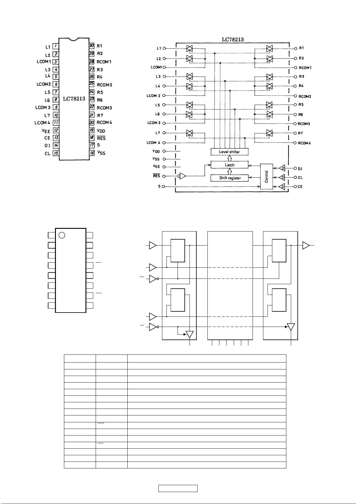
LC78213-E (IC613,614,166,617)
f
74HC595D (IC804,805,806,807)
Q1
Q2
Q3
Q4
Q5
Q6
Q7
GND
1
2
3
4
595
5
6
7
8
16
15
14
13
12
11
10
9
V
CC
Q0
DS
OE
ST_CP
SH_CP
MR
Q7'
PIN SYMBOL DESCRIPTION
1 Q1 parallel data output
2 Q2 parallel data output
3 Q3 parallel data output
4 Q4 parallel data output
5 Q5 parallel data output
6 Q6 parallel data output
7 Q7 parallel data output
8 GND ground (0 V)
9 Q7’ serial data output
10
MR master reset (active LOW)
11 SH_CP shift register clock input
12 ST_CP storage register clock input
13
OE output enable (active LOW)
14 DS serial data input
15 Q0 parallel data output
16 V
CC
ull pagewidth
DS
SH_CP
MR
ST_CP
OE
positive supply voltage
STAGE 0 STAGES 1 to 6 STAGE 7
DCPQ
FF0
R
DCPQ
LATCH
DQ
Q0
Q1 Q2 Q3 Q4 Q5 Q6 Q7
DCPQ
FF7
R
DCPQ
LATCH
Q7'
MLA010
10
DN-X1100
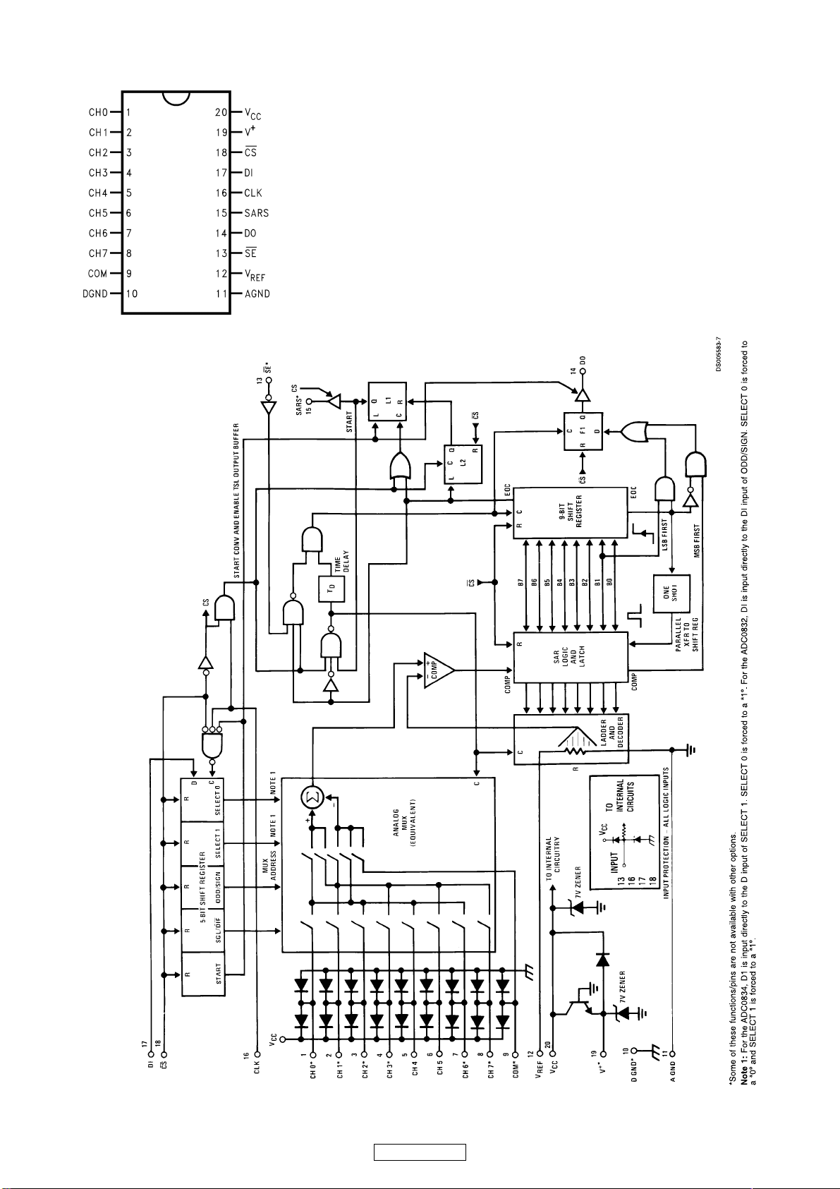
ADC0838CCWM (IC802)
BLOCK DIAGRAM
11
DN-X1100

--MEMO--
12
DN-X1100
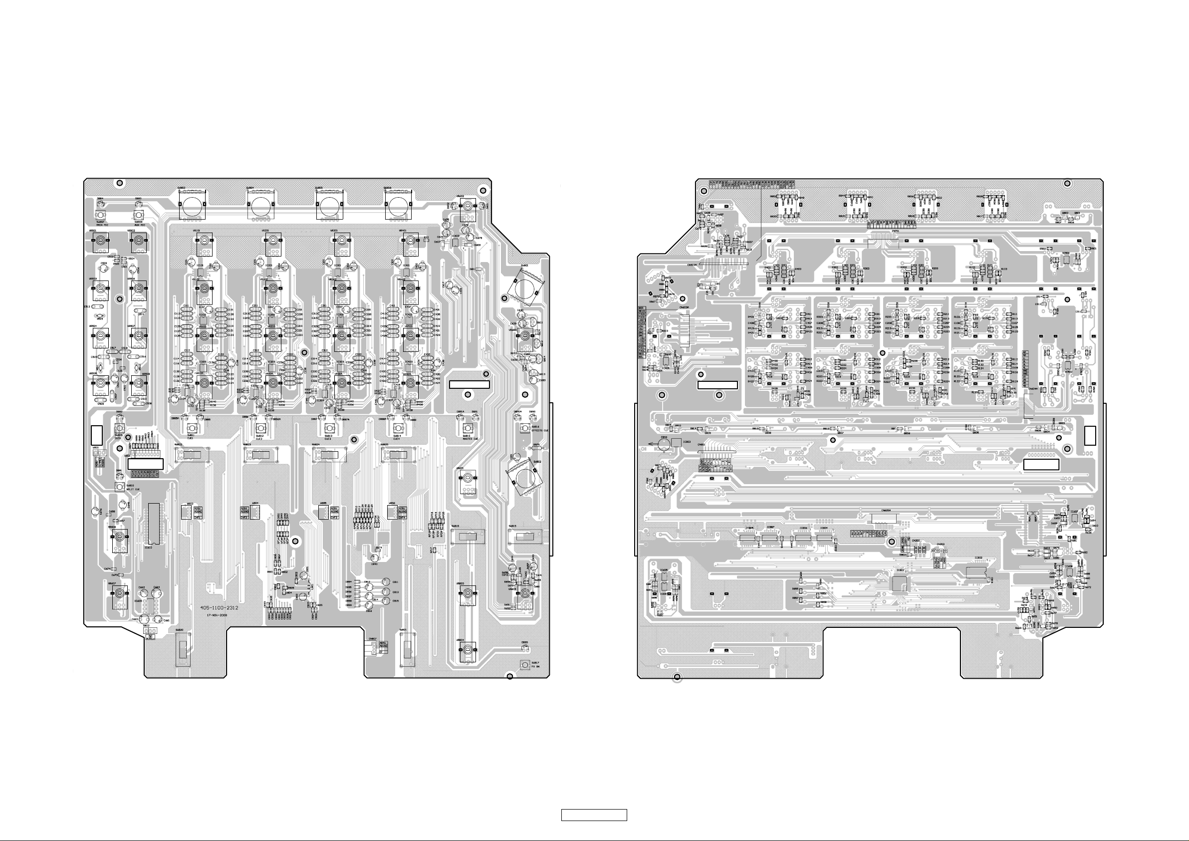
PRINTED WIRING BOARDS
MIXER P.W.B. UNIT
COMPONENT SIDE
FOIL SIDE
13
DN-X1100

TRANSFER P.W.B. UNIT
COMPONENT SIDE
14
DN-X1100
FOIL SIDE

IO P.W.B. UNIT
COMPONENT SIDE
15
DN-X1100
FOIL SIDE

POWER/PHONE P.W.B. UNIT
COMPONENT SIDE
16
DN-X1100
FOIL SIDE

LEVEL METER P.W.B. UNIT
COMPONENT SIDE
17
DN-X1100
FOIL SIDE

CH FADER P.W.B. UNIT AC P.W.B. UNIT
COMPONENT SIDE
FOIL SIDECOMPONENT SIDE
18
DN-X1100

NOTE FOR PARTS LIST
1.
Parts for which "nsp" is indicated on this table cannot be supplied.
When ordering of part, clearly indicate "1" and "I" (i) to avoid mis-supplying.
2.
Ordering part without stating its part number can not be supplied.
3.
Part indicated with the mark "★" is not illustrated in the exploded view.
4.
Not including General-purpose Carbon Film Resistor in the P.W.Board parts list. (Refer to the Schematic Diagram for those parts.)
5.
Not including General-purpose Carbon Chip Resistor in the P.W.Board parts list. (Refer to the Schematic Diagram for those parts.)
6.
WARNING:
Parts marked with this symbol z have critical characteristics.
Use ONLY replacement parts recommended by the manufacturer.
● Resistors
Ex.: RN
Type
RD : Carbon
RC : Composition
RS : Metal oxide film
RW: winding
RN : Metal film
RK : Metal mixture
* Resistance
2
14K
Shape
and performance
Indicates number of zeros after effective number.
2-digit effective number.
2E
Power
2B : 1/8 W
2E : 1/4 W
2H : 1/2 W
3A : 1 W
3D : 2 W
3F : 3 W
3H : 5 W
1800ohm=1.8kohm18
182
Resistance
F:±1%
G:±2%
J:±5%
K:±10%
M:±20%
G
Allowable
error
P : Pulse-resistant type
NL : Low noise type
NB : Non-burning type
FR : Fuse-resistor
F : Lead wire forming
FR
Others
: Units: ohm
● Capacitors
Ex.: CE
Type
CE : Aluminum foil
electrolytic
CA : Aluminium solid
electrolytic
CS : Tantalum electrolytic
CQ : Film
CK : Ceramic
CC : Ceramic
CP : Oil
CM: Mica
CF : Metallized
CH : Metallized
* Capacity (electrolyte only)
2
Indicates number of zeros after effective number.
・ Units:μF.
2-digit effective number.
1.2ohm1R 2
1-digit effective number.
2-digit effective number, decimal point indicated by R.
04W
Shape
and performance
2200μF22
1H
Dielectric
strength
0J : 6.3 V
1A : 10 V
1C : 16 V
1E : 25 V
1V : 35 V
1H : 50 V
2A : 100 V
2B : 125 V
2C : 160 V
2D : 200 V
2E : 250 V
2H : 500 V
2J : 630 V
3R2
CapacityMAllowable
error
F:±1%
G:±2%
J:±5%
K:±10%
M:±20%
Z:±80%
: - 20%
P : +100%
C:±0.25pF
D:±0.5pF
= : Others
Others
BP
HS : High stability type
BP : Non-polar type
HR : Ripple-resistant type
DL : For change and discharge
HF : For assuring high requency
U : UL part
C : CSA part
W : UL-CSA part
F : Lead wire forming
2
・ Units:μF.
2.2μF2R
1-digit effective number.
2-digit effective number, decimal point indicated by R
* Capacity (except electrolyte)
2
・ Units:pF
・ When the dielectric strength is indicated in AC,"AC" is included after the dieelectric strength value.
2200pF=0.0022μF22
Indicates number of zeros after efective number.
(More than 2)
2-digit effective number.
1
・ Units:pF
Indicates number of zeros after effective numver.
(0 or 1)
2-digit effective number.
19
DN-X1100
220pF22

PARTS LIST OF P.W.B. UNIT
* Parts for which "nsp" is indicated on this table cannot be supplied.
* The parts listed below are for maintenance only, might differ from the parts used in the unit in appearances or dimensions.
Note: The symbols in the column "Remarks" indicate the following destinations.
E3: U.S.A. & Canada model E2: Europe model
MIXER & TRANSFER P.W.B. UNIT ASS'Y
Ref. No. Part No. Part Name Remarks Q'ty New
SEMICONDUCTORS GROUP
IC101 00D9587059407 IC(BA15218F/BA15218FE2)
IC102,103 00D9587035900 IC(NJM-2060V-TE1)
IC104 00D9587059407 IC(BA15218F/BA15218FE2)
IC105 00D9587036103 IC(M51132L)
IC107 00D9587059407 IC(BA15218F/BA15218FE2)
IC11 00D9410022103 IC(7812)
IC110 00D9587059106 IC(NJM-4558M)
IC112 00D9587059106 IC(NJM-4558M)
IC201 00D9587059407 IC(BA15218F/BA15218FE2)
IC202,203 00D9587035900 IC(NJM-2060V-TE1)
IC204 00D9587059407 IC(BA15218F/BA15218FE2)
IC205 00D9587059601 IC(M51132L)
IC207 00D9587059407 IC(BA15218F/BA15218FE2)
IC212 00D9587059106 IC(NJM-4558M)
IC301 00D9587059407 IC(BA15218F/BA15218FE2)
IC302,303 00D9587035900 IC(NJM-2060V-TE1)
IC304 00D9587059407 IC(BA15218F/BA15218FE2)
IC305 00D9587059601 IC(M51132L)
IC307 00D9587059407 IC(BA15218F/BA15218FE2)
IC310 00D9587059106 IC(NJM-4558M)
IC312 00D9587059106 IC(NJM-4558M)
IC401 00D9587059407 IC(BA15218F/BA15218FE2)
IC402,403 00D9587035900 IC(NJM-2060V-TE1)
IC404 00D9587059407 IC(BA15218F/BA15218FE2)
IC405 00D9587059601 IC(M51132L)
IC407 00D9587059407 IC(BA15218F/BA15218FE2)
IC412 00D9587059106 IC(NJM-4558M)
IC501 00D9587058903 IC(NJM-2068M)
IC502 00D9587059407 IC(BA15218F/BA15218FE2)
IC601-608 00D9587059407 IC(BA15218F/BA15218FE2)
IC609 00D9580073804 INTEGRATED CIRCUIT(NJM-4556AD)
IC610-612 00D9587058806 IC(LC78212)
IC613,614 00D9587058408 IC(LC78213)
IC615 00D9587058806 IC(LC78212)
IC616,617 00D9587058408 IC(LC78213)
IC618 00D9587059407 IC(BA15218F/BA15218FE2)
IC801 941243001180S CONTROL IC ASS'Y
IC(MC9S08AW32CPUE)
IC802 00D9587058000 IC(ADC0838CCWM)
IC803 00D9587058204 IC(BA033FP)
IC804-807 00D9587058709 IC(74HC595D/74AHC595D/74AHC595DR)
417-QMX2-167
417-PRO1000-502
417-QMX2-167
417-SA12-487
417-QMX2-167
417-BJ1900L-231
417-PS2-577
417-PS2-577
417-QMX2-167
417-PRO1000-502
417-QMX2-167
417-SA12-487
417-QMX2-167
417-PS2-577
417-QMX2-167
417-PRO1000-502
417-QMX2-167
417-SA12-487
417-QMX2-167
417-PS2-577
417-PS2-577
417-QMX2-167
417-PRO1000-502
417-QMX2-167
417-SA12-487
417-QMX2-167
417-PS2-577
417-M5-582
417-QMX2-167
417-QMX2-167
417-3113-018
417-HMA2200-5030
417-DRM120-510
417-HMA2200-5030
417-DRM120-510
417-QMX2-167
704-X1100-8186 *
417-900-747
417-CTB200-500
417-HDJ9800-643
Q11 00D9587057506 TRANSISTOR(DTA124EKA)
Q12 00D9587057700 TRANSISTOR(DTC114EKAT146)
Q605-610 00D9410046406 TRANSISTOR(2SC4695-TB-E)
Q611,612 00D9587034707 TRANSISTOR(2SC2878-B)
Q613 941219001170S TRANSISTOR(2SB892S(T))
Q614 90M-HT400500R TRANSISTOR(2SD1207/2SD1207S(T))
20
DN-X1100
416-CTB200-178
416-HDJ2460-234
416-DAIA-273
416-AMC110A-5017
416-1360S-017A
416-1360S-016
*

Ref. No. Part No. Part Name Remarks Q'ty New
Q801-810 00D9587057700 TRANSISTOR(DTC114EKAT146)
416-HDJ2460-234
D101,102 00D9587056701 DIODE(RB160M-30)
D201,202 00D9587056701 DIODE(RB160M-30)
D301,302 00D9587056701 DIODE(RB160M-30)
D401,402 00D9587056701 DIODE(RB160M-30)
D601,602 00D9587051706 LED(RED,LTL-16KE)
D603,604 00D9587056701 DIODE(RB160M-30)
D607-610 00D9587056701 DIODE(RB160M-30)
D611 00D9410046901 SWITCHING DIODE(1SS355)
D881 00D9587052006 LED ( LTL1CHJSDNN,YELLOW )
D882 941263001070S LED(LTL1CHKGKNN,GREEN)
D883,884 941263001060S LED(LTL1CHJEDNN,RED)
D885-888 00D9587052006 LED ( LTL1CHJSDNN,YELLOW )
D885A-888A 00D9587052006 LED ( LTL1CHJSDNN,YELLOW )
D889-891 00D9587052006 LED ( LTL1CHJSDNN,YELLOW )
D890A,891A 00D9587052006 LED ( LTL1CHJSDNN,YELLOW )
D894-899 00D9410046901 SWITCHING DIODE(1SS355)
RESISTORS GROUP
R13 nsp CARBON FILM RESISTOR(1.5 OHM)
RB601,602 nsp
THICK FILM RESISTOR NETWORKS(47K OHM,J)
414-900-208
414-900-208
414-900-208
414-900-208
410-CD6000-122
414-900-208
414-900-208
414-CD1000-075
410-HDJ2000-162
410-TT2A3SL-250
410-DJ5000-253
410-HDJ2000-162
410-HDJ2000-162
410-HDJ2000-162
410-HDJ2000-162
414-CD1000-075
412-U101-1179
412-X1100-1338
*
*
CAPACITORS GROUP
C21 nsp CHIP CAPACITOR(0.1uF/50V,Z)
C25 nsp CHIP CAPACITOR(0.1uF/50V,Z)
C26 941134001250S ELEC. CAPACITOR(220uF/25V)
C101,102 00D9587056303 ELEC. CAPACITOR(10uF/25V,M)
C103,104 nsp CHIP CAPACITOR(1000pF/50V,K)
C105,106 nsp CHIP CAPACITOR(15pF/50V,J)
C107-110 nsp CHIP CAPACITOR(1000pF/50V,K)
C111,112 00D9587054208 POLYESTER CAPACITOR(0.0082uF/100V,J)
C113-116 00D9587053801 POLYESTER CAPACITOR(0.0018uF/100V,J)
C117,118 nsp CHIP CAPACITOR(1000pF/50V,K)
C119,120 00D9587054208 POLYESTER CAPACITOR(0.0082uF/100V,J)
C121,122 00D9587054703 POLYESTER CAPACITOR(820pF/50V,J)
C123,124 nsp POLYESTER CAPACITOR(0.0047uF/100V,J)
C125,126 00D9587056109 POLYESTER CAPACITOR(0.1uF/63V,J)
C127-130 00D9587054402 POLYESTER CAPACITOR(0.022uF/100V,J)
C131,132 00D9587056109 POLYESTER CAPACITOR(0.1uF/63V,J)
C133,134 00D9587054305 POLYESTER CAPACITOR(0.01uF/100V,J)
C135,136 00D9587054606 POLYESTER CAPACITOR(0.056uF/100V,J)
C137,138 00D9587056303 ELEC. CAPACITOR(10uF/25V,M)
C139,140 nsp CHIP CAPACITOR(33pF/50V,J)
C141,142 00D9587056400 ELEC. CAPACITOR(22uF/16V,M)
C143,144 nsp CHIP CAPACITOR(1000pF/50V,K)
C145,146 00D9587056206 ELEC. CAPACITOR(1uF/50V,M)
C147 00D9587056400 ELEC. CAPACITOR(22uF/16V,M)
C149 nsp CHIP CAPACITOR(0.1uF/50V,Z)
C150 nsp CHIP CAPACITOR(1000pF/50V,K)
C151 nsp CHIP CAPACITOR(0.33uF/16V,Z)
C152 nsp CHIP CAPACITOR(0.22uF/50V,J)
C153,154 00D9587056206 ELEC. CAPACITOR(1uF/50V,M)
413-DCM280-773
413-DCM280-773
413-X1100-1123
413-SPPW3-235
413-DCM280-768
413-007USB-781
413-DCM280-768
413-900-937
413-900-932
413-DCM280-768
413-900-937
413-EFX2-886
413-HT8015-159
413-SPPW3-083
413-900-939
413-SPPW3-083
413-900-938
413-900-941
413-SPPW3-235
413-900-926
413-SPPW3-236
413-DCM280-768
413-SPPW3-234
413-SPPW3-236
413-DCM280-773
413-DCM280-768
413-007USB-782
413-900-942
413-SPPW3-234
*
21
DN-X1100

Ref. No. Part No. Part Name Remarks Q'ty New
C155,156 nsp CHIP CAPACITOR(1000pF/50V,K)
C157,158 nsp CHIP CAPACITOR(33pF/50V,J)
C159,160 00D9587055304 ELEC. CAPACITOR(4.7uF/50V,M)
C177,178 nsp CHIP CAPACITOR(1000pF/50V,K)
C201,202 00D9587056303 ELEC. CAPACITOR(10uF/25V,M)
C203,204 nsp CHIP CAPACITOR(1000pF/50V,K)
C205,206 nsp CHIP CAPACITOR(15pF/50V,J)
C207-210 nsp CHIP CAPACITOR(1000pF/50V,K)
C211,212 00D9587054208 POLYESTER CAPACITOR(0.0082uF/100V,J)
C213 00D9587053801 POLYESTER CAPACITOR(0.0018uF/100V,J)
C214-216 00D9587053801 POLYESTER CAPACITOR(0.0018uF/100V,J)
C217,218 nsp CHIP CAPACITOR(1000pF/50V,K)
C219,220 00D9587054208 POLYESTER CAPACITOR(0.0082uF/100V,J)
C221,222 00D9587054703 POLYESTER CAPACITOR(820pF/50V,J)
C223,224 nsp POLYESTER CAPACITOR(0.0047uF/100V,J)
C225,226 00D9587056109 POLYESTER CAPACITOR(0.1uF/63V,J)
C227-230 00D9587054402 POLYESTER CAPACITOR(0.022uF/100V,J)
C231,232 00D9587056109 POLYESTER CAPACITOR(0.1uF/63V,J)
C233,234 00D9587054305 POLYESTER CAPACITOR(0.01uF/100V,J)
C235,236 00D9587054606 POLYESTER CAPACITOR(0.056uF/100V,J)
C237,238 00D9587056303 ELEC. CAPACITOR(10uF/25V,M)
C239,240 nsp CHIP CAPACITOR(33pF/50V,J)
C241,242 00D9587056400 ELEC. CAPACITOR(22uF/16V,M)
C243,244 nsp CHIP CAPACITOR(1000pF/50V,K)
C245,246 00D9587056206 ELEC. CAPACITOR(1uF/50V,M)
C247 00D9587056400 ELEC. CAPACITOR(22uF/16V,M)
C249 nsp CHIP CAPACITOR(0.1uF/50V,Z)
C250 nsp CHIP CAPACITOR(1000pF/50V,K)
C251 nsp CHIP CAPACITOR(0.33uF/16V,Z)
C252 nsp CHIP CAPACITOR(0.22uF/50V,J)
C253,254 00D9587056206 ELEC. CAPACITOR(1uF/50V,M)
C255,256 nsp CHIP CAPACITOR(1000pF/50V,K)
C257,258 nsp CHIP CAPACITOR(33pF/50V,J)
C259,260 00D9587055304 ELEC. CAPACITOR(4.7uF/50V,M)
C301,302 00D9587056303 ELEC. CAPACITOR(10uF/25V,M)
C303,304 nsp CHIP CAPACITOR(1000pF/50V,K)
C305,306 nsp CHIP CAPACITOR(15pF/50V,J)
C307-310 nsp CHIP CAPACITOR(1000pF/50V,K)
C311,312 00D9587054208 POLYESTER CAPACITOR(0.0082uF/100V,J)
C313-316 00D9587053801 POLYESTER CAPACITOR(0.0018uF/100V,J)
C317,318 nsp CHIP CAPACITOR(1000pF/50V,K)
C319,320 00D9587054208 POLYESTER CAPACITOR(0.0082uF/100V,J)
C321,322 00D9587054703 POLYESTER CAPACITOR(820pF/50V,J)
C323,324 nsp POLYESTER CAPACITOR(0.0047uF/100V,J)
C325,326 00D9587056109 POLYESTER CAPACITOR(0.1uF/63V,J)
C327-330 00D9587054402 POLYESTER CAPACITOR(0.022uF/100V,J)
C331,332 00D9587056109 POLYESTER CAPACITOR(0.1uF/63V,J)
C333,334 00D9587054305 POLYESTER CAPACITOR(0.01uF/100V,J)
C335,336 00D9587054606 POLYESTER CAPACITOR(0.056uF/100V,J)
C337,338 00D9587056303 ELEC. CAPACITOR(10uF/25V,M)
C339,340 nsp CHIP CAPACITOR(33pF/50V,J)
C341,342 00D9587056400 ELEC. CAPACITOR(22uF/16V,M)
C343,344 nsp CHIP CAPACITOR(1000pF/50V,K)
C345,346 00D9587056206 ELEC. CAPACITOR(1uF/50V,M)
C347 00D9587056400 ELEC. CAPACITOR(22uF/16V,M)
C349 nsp CHIP CAPACITOR(0.1uF/50V,Z)
413-DCM280-768
413-900-926
413-HT801K-191
413-DCM280-768
413-SPPW3-235
413-DCM280-768
413-007USB-781
413-DCM280-768
413-900-937
413-900-932
413-900-932
413-DCM280-768
413-900-937
413-EFX2-886
413-HT8015-159
413-SPPW3-083
413-900-939
413-SPPW3-083
413-900-938
413-900-941
413-SPPW3-235
413-900-926
413-SPPW3-236
413-DCM280-768
413-SPPW3-234
413-SPPW3-236
413-DCM280-773
413-DCM280-768
413-007USB-782
413-900-942
413-SPPW3-234
413-DCM280-768
413-900-926
413-HT801K-191
413-SPPW3-235
413-DCM280-768
413-007USB-781
413-DCM280-768
413-900-937
413-900-932
413-DCM280-768
413-900-937
413-EFX2-886
413-HT8015-159
413-SPPW3-083
413-900-939
413-SPPW3-083
413-900-938
413-900-941
413-SPPW3-235
413-900-926
413-SPPW3-236
413-DCM280-768
413-SPPW3-234
413-SPPW3-236
413-DCM280-773
22
DN-X1100

Ref. No. Part No. Part Name Remarks Q'ty New
C350 nsp CHIP CAPACITOR(1000pF/50V,K)
C351 nsp CHIP CAPACITOR(0.33uF/16V,Z)
C352 nsp CHIP CAPACITOR(0.22uF/50V,J)
C353,354 00D9587056206 ELEC. CAPACITOR(1uF/50V,M)
C355,356 nsp CHIP CAPACITOR(1000pF/50V,K)
C357,358 nsp CHIP CAPACITOR(33pF/50V,J)
C359,360 00D9587055304 ELEC. CAPACITOR(4.7uF/50V,M)
C377,378 nsp CHIP CAPACITOR(1000pF/50V,K)
C401,402 00D9587056303 ELEC. CAPACITOR(10uF/25V,M)
C403,404 nsp CHIP CAPACITOR(1000pF/50V,K)
C405,406 nsp CHIP CAPACITOR(15pF/50V,J)
C407-410 nsp CHIP CAPACITOR(1000pF/50V,K)
C411,412 00D9587054208 POLYESTER CAPACITOR(0.0082uF/100V,J)
C413-416 00D9587053801 POLYESTER CAPACITOR(0.0018uF/100V,J)
C417,418 nsp CHIP CAPACITOR(1000pF/50V,K)
C419,420 00D9587054208 POLYESTER CAPACITOR(0.0082uF/100V,J)
C421,422 00D9587054703 POLYESTER CAPACITOR(820pF/50V,J)
C423,424 nsp POLYESTER CAPACITOR(0.0047uF/100V,J)
C425,426 00D9587056109 POLYESTER CAPACITOR(0.1uF/63V,J)
C427-430 00D9587054402 POLYESTER CAPACITOR(0.022uF/100V,J)
C431,432 00D9587056109 POLYESTER CAPACITOR(0.1uF/63V,J)
C433,434 00D9587054305 POLYESTER CAPACITOR(0.01uF/100V,J)
C435,436 00D9587054606 POLYESTER CAPACITOR(0.056uF/100V,J)
C437,438 00D9587056303 ELEC. CAPACITOR(10uF/25V,M)
C439,440 nsp CHIP CAPACITOR(33pF/50V,J)
C441,442 00D9587056400 ELEC. CAPACITOR(22uF/16V,M)
C443,444 nsp CHIP CAPACITOR(1000pF/50V,K)
C445,446 00D9587056206 ELEC. CAPACITOR(1uF/50V,M)
C447 00D9587056400 ELEC. CAPACITOR(22uF/16V,M)
C449 nsp CHIP CAPACITOR(0.1uF/50V,Z)
C450 nsp CHIP CAPACITOR(1000pF/50V,K)
C451 nsp CHIP CAPACITOR(0.33uF/16V,Z)
C452 nsp CHIP CAPACITOR(0.22uF/50V,J)
C453,454 00D9587056206 ELEC. CAPACITOR(1uF/50V,M)
C455,456 nsp CHIP CAPACITOR(1000pF/50V,K)
C457,458 nsp CHIP CAPACITOR(33pF/50V,J)
C459,460 00D9587055304 ELEC. CAPACITOR(4.7uF/50V,M)
C501,502 nsp CHIP CAPACITOR(1000pF/50V,K)
C503 00D9587056400 ELEC. CAPACITOR(22uF/16V,M)
C504 nsp CHIP CAPACITOR(12pF/50V J)
C505 nsp CHIP CAPACITOR(15pF/50V,J)
C506 00D9587056400 ELEC. CAPACITOR(22uF/16V,M)
C507-510 00D9587054509 POLYESTER CAPACITOR(0.039uF/100V,J)
C511,512 nsp CHIP CAPACITOR(270pF/50V,J)
C513,514 00D9587053908 POLYESTER CAPACITOR(0.0033uF/100V,J)
C515-518 00D9587054101 POLYESTER CAPACITOR(0.0056uF/100V,J)
C519,520 nsp CHIP CAPACITOR(22pF/50V,J)
C521,522 00D9587056303 ELEC. CAPACITOR(10uF/25V,M)
C525-628 nsp CHIP CAPACITOR(1000pF/50V,K)
C601-616 nsp CHIP CAPACITOR(1000pF/50V,K)
C617,618 00D9587056303 ELEC. CAPACITOR(10uF/25V,M)
C619,620 nsp CHIP CAPACITOR(1000pF/50V,K)
C621,622 nsp CHIP CAPACITOR(33pF/50V,J)
C623,624 nsp CHIP CAPACITOR(47pF/50V,J)
C629,630 00D9587055304 ELEC. CAPACITOR(4.7uF/50V,M)
C631,632 nsp CHIP CAPACITOR(1000pF/50V,K)
413-DCM280-768
413-007USB-782
413-900-942
413-SPPW3-234
413-DCM280-768
413-900-926
413-HT801K-191
413-DCM280-768
413-SPPW3-235
413-DCM280-768
413-007USB-781
413-DCM280-768
413-900-937
413-900-932
413-DCM280-768
413-900-937
413-EFX2-886
413-HT8015-159
413-SPPW3-083
413-900-939
413-SPPW3-083
413-900-938
413-900-941
413-SPPW3-235
413-900-926
413-SPPW3-236
413-DCM280-768
413-SPPW3-234
413-SPPW3-236
413-DCM280-773
413-DCM280-768
413-007USB-782
413-900-942
413-SPPW3-234
413-DCM280-768
413-900-926
413-HT801K-191
413-DCM280-768
413-SPPW3-236
413-DCM280-809
413-007USB-781
413-SPPW3-236
413-900-940
413-U5000-1004
413-900-934
413-900-936
413-CR701-5161
413-SPPW3-235
413-DCM280-768
413-DCM280-768
413-SPPW3-235
413-DCM280-768
413-900-926
413-007USB-784
413-HT801K-191
413-DCM280-768
23
DN-X1100

Ref. No. Part No. Part Name Remarks Q'ty New
C633,634 nsp CHIP CAPACITOR(120pF/50V,J)
C639,640 nsp CHIP CAPACITOR(1000pF/50V,K)
C641,642 nsp CHIP CAPACITOR(22pF/50V,J)
C643,644 00D9587056400 ELEC. CAPACITOR(22uF/16V,M)
C645,646 00D9587055304 ELEC. CAPACITOR(4.7uF/50V,M)
C647,648 nsp CHIP CAPACITOR(22pF/50V,J)
C649,650 nsp CHIP CAPACITOR(1000pF/50V,K)
C651,652 00D9587056400 ELEC. CAPACITOR(22uF/16V,M)
C653,654 nsp CHIP CAPACITOR(22pF/50V,J)
C655-658 nsp CHIP CAPACITOR(1000pF/50V,K)
C659,660 nsp CHIP CAPACITOR(22pF/50V,J)
C661,662 00D9587055304 ELEC. CAPACITOR(4.7uF/50V,M)
C663,664 941134001280S ELEC. CAPACITOR(100uF/25V,M)
C665,666 nsp CHIP CAPACITOR(47pF/50V,J)
C669,670 00D9587056400 ELEC. CAPACITOR(22uF/16V,M)
C672 nsp CHIP CAPACITOR(0.01uF/50V,K)
C673,674 nsp CHIP CAPACITOR(1000pF/50V,K)
C675-678 941134001290S ELEC. CAPACITOR(0.22uF/50V,M)
C679,680 nsp CHIP CAPACITOR(1000pF/50V,K)
C681,682 nsp CHIP CAPACITOR(22pF/50V,J)
C683,684 941134001300S ELEC. CAPACITOR(22uF/25V,M)
C801 00D9587054907 ELEC. CAPACITOR(100uF/10V,M)
C802 nsp CHIP CAPACITOR(0.1uF/50V,Z)
C803 00D9587054907 ELEC. CAPACITOR(100uF/10V,M)
C804 nsp CHIP CAPACITOR(0.1uF/50V,Z)
C807-809 nsp CHIP CAPACITOR(0.1uF/50V,Z)
C811-814 00D9587056206 ELEC. CAPACITOR(1uF/50V,M)
C815,816 90M-EJ000100R ELEC. CAPACITOR(0.47uF/50V,M)
C819 nsp CHIP CAPACITOR(0.1uF/50V,Z)
C823-836 nsp CHIP CAPACITOR(0.01uF/50V,K)
C840 00D9587030701 ELEC. CAPACITOR(2.2uF/50V,M)
C842-845 nsp CHIP CAPACITOR(0.1uF/50V,Z)
C846 941134000530S ELEC. CAPACITOR(470uF/10V,M)
C847-850 nsp CHIP CAPACITOR(0.1uF/50V,Z)
C851 00D9587054907 ELEC. CAPACITOR(100uF/10V,M)
413-900-930
413-DCM280-768
413-CR701-5161
413-SPPW3-236
413-HT801K-191
413-CR701-5161
413-DCM280-768
413-SPPW3-236
413-CR701-5161
413-DCM280-768
413-CR701-5161
413-HT801K-191
413-X050-1068
413-007USB-784
413-SPPW3-236
413-DCM280-771
413-DCM280-768
413-SPPW3-305
413-DCM280-768
413-CR701-5161
413-CDMIX2-631
413-HMA2200-5017
413-DCM280-773
413-HMA2200-5017
413-DCM280-773
413-DCM280-773
413-SPPW3-234
413-SPPW3-233
413-DCM280-773
413-DCM280-771
413-DV300-5156
413-DCM280-773
413-HT8015-169
413-DCM280-773
413-HMA2200-5017
*
*
*
*
OTHER PARTS GROUP
CN202 nsp
CN203 nsp 4P 2.54 SERIES STRIP PIN HEADER(H=6mm)
CN603A,603B 00D9587049802 17P 1.0 FFC CONNECTOR(52207-1785)
CN604A,605A 90M-YJ003030R 12P 1.0 FFC CONNECTOR(52207-1285)
CN604B,605B 90M-YJ003030R 12P 1.0 FFC CONNECTOR(52207-1285)
CN701 00D9410047308 16P 1.0 FFC CONNECTOR(52207-1685)
CN801 941644001140S 21P 1.0 FFC CONNECTOR(52808-2170)
CN807 00D9587066306 4P SOCKET(CKM2001WR-4P)
CN903A 941644001150S 28P 1.0 FFC SOCKET(52808-2870)
L801 941115001080S INDUCTOR(10uH,AL0204ST-100K-S-A)
SW801 941663001050S ROATRY SW(SR1712F-0105-25F0A-N9-N)
SW802-806 941663001040S ROATRY SW(SR1712F-0108-25F0A-N9-N)
SW807-817 941662001160S TACT SW(SFKHVBE3525-HF
SW818-821 941664001020S SLIDE SW(SKA-12-12)
SW822-825 941664001030S SLIDE SW(SKA-13-12B)
2*3P 2.54 SERIES STRIP PIN HEADER(H=6mm) 424-SDJ2-142
24
DN-X1100
424-HDJ9700-069
404-900-2107
404-4001-2235
404-4001-2235
404-HV3423K-583
404-S300-2531
404-DCM270E3-878A
404-X1100-3059
415-HMD5000-097
403-X1100-347
403-X1100-346
403-DCM270X-101A
403-QMX1-063A
403-X1100-345
*
*
*
*
*
*
*
*

Ref. No. Part No. Part Name Remarks Q'ty New
VR101 00D9410059707 ROTARY VR(20K(A)*2)
VR102-104 941679001120S ROTARY VR(20K(3B)*2)
VR201 00D9410059707 ROTARY VR(20K(A)*2)
VR202-204 941679001120S ROTARY VR(20K(3B)*2)
VR301 00D9410059707 ROTARY VR(20K(A)*2)
VR302-304 941679001120S ROTARY VR(20K(3B)*2)
VR401 00D9410059707 ROTARY VR(20K(A)*2)
VR402-404 941679001120S ROTARY VR(20K(3B)*2)
VR501,502 941679001090S ROTARY VR(20K(A))
VR503-508 941679001110S ROTARY VR(50K(B))
VR601 00D9410059309 ROTARY VR(50K(MN)*2)
VR602 00D9587059805 ROTARY VR(20KA*2)
VR603 00D9410059707 ROTARY VR(20K(A)*2)
VR604 941679001130S ROTART VR(50K(3B)*2)
VR606 00D9410059202 ROTARY VR(50K(3B)*2)
VR607 00D9410059707 ROTARY VR(20K(A)*2)
VR803,804 941679001100S ROTARY VR(20K(B))
418-X050-446
418-X1100-530
418-X050-446
418-X1100-530
418-X050-446
418-X1100-530
418-X050-446
418-X1100-530
418-X1100-527
418-X1100-529
418-X050-332
418-900-284
418-X050-446
418-X1100-550
418-X050-252
418-X050-446
418-X1100-528
*
*
*
*
*
*
*
*
W501 nsp 3P 2.5 CONNECTOR WIRE(L=250mm)
W602 nsp 3P 2.5 CONNECTOR WIRE(L=60mm)
W702 nsp 4P 2.5 CONNECTOR WIRE(L=250mm)
W803-806 nsp 4P 2.0 CONNECTOR WIRE(L=55mm)
W901 nsp 9P 2.0 CONNECTOR WIRE(L=310mm)
941606000980S 12P 1.0 FFC CABLE(L=70mm) CN605A-605B
941606000990S 12P 1.0 FFC CABLE(L=70mm) CN604A-604B
941606001000S 17P 1.0 FFC CABLE(L=60mm) CN603A-603B
941606001010S 16P 1.0 FFC CABLE(L=150mm) CN701
00D9587062203 LED HOLDER D601,602
nsp SPACER SUPPORT(H-17)
nsp CUSHION
00D9410019501
SCREW(SAE1018,φ3*L8*P0.5)
404-MCX-2026
404-MU12-2661
404-X1100-3073
404-X1100-3079
404-X1100-3078
406-SDJ1F-968
406-X1100-1033
406-X1100-1034
406-X1100-1035
504-CDT1000-091
504-SPANDMK2-156
612-390-234
602-2002-085
*
*
*
*
25
DN-X1100

IO P.W.B. UNIT ASS'Y
Ref. No. Part No. Part Name Remarks Q'ty New
SEMICONDUCTORS GROUP
IC114,115 00D9410021609 IC(NJM-4580M-TE2)
IC116 00D9587059203 IC(LC78211-E)
IC214,215 00D9410021609 IC(NJM-4580M-TE2)
IC216 00D9587059203 IC(LC78211-E)
IC314,315 00D9410021609 IC(NJM-4580M-TE2)
IC316 00D9587059203 IC(LC78211-E)
IC414,415 00D9410021609 IC(NJM-4580M-TE2)
IC416 00D9587059203 IC(LC78211-E)
IC511 00D9587058903 IC(NJM-2068M)
RESISTORS GROUP
R07,08 nsp CARBON FILM RESISTOR(100 OHM,1/4W,J)
RB701,702 nsp
CAPACITORS GROUP
C005,006 nsp CHIP CAPACITOR( 220pF/50V)
C007-010 nsp CHIP CAPACITOR(100pF/50V,J)
C011,012 nsp CHIP CAPACITOR( 220pF/50V)
C013-024 nsp CHIP CAPACITOR(100pF/50V,J)
C031,032 nsp CHIP CAPACITOR(100pF/50V,J)
C17,18 00D9587030604 ELEC. CAPACITOR(220uF/25V,M)
C193,194 nsp CHIP CAPACITOR(100pF/50V,J)
C195,196 nsp CHIP CAPACITOR(1000pF/50V,K)
C197,198 00D9587056400 ELEC. CAPACITOR(22uF/16V,M)
C293,294 nsp CHIP CAPACITOR(100pF/50V,J)
C295,296 nsp CHIP CAPACITOR(1000pF/50V,K)
C297,298 00D9587056400 ELEC. CAPACITOR(22uF/16V,M)
C393,394 nsp CHIP CAPACITOR(100pF/50V,J)
C395,396 nsp CHIP CAPACITOR(1000pF/50V,K)
C397,398 00D9587056400 ELEC. CAPACITOR(22uF/16V,M)
C493,494 nsp CHIP CAPACITOR(100pF/50V,J)
C495,496 nsp CHIP CAPACITOR(1000pF/50V,K)
C497,498 00D9587056400 ELEC. CAPACITOR(22uF/16V,M)
C541,542 nsp CHIP CAPACITOR( 220pF/50V)
C543,544 00D9587056400 ELEC. CAPACITOR(22uF/16V,M)
C545,546 nsp CHIP CAPACITOR(22pF/50V,J)
C547,548 nsp CHIP CAPACITOR(1000pF/50V,K)
C549,565 00D9587056303 ELEC. CAPACITOR(10uF/25V,M)
C551,552 nsp CHIP CAPACITOR( 220pF/50V)
C555,556 00D9587056400 ELEC. CAPACITOR(22uF/16V,M)
C563,564 nsp CHIP CAPACITOR(22pF/50V,J)
C701,702 nsp CHIP CAPACITOR(100pF/50V,J)
C703,704 nsp E/C(47uF/16V,M)
C705,706 00D9587053607 POLYESTER CAPACITOR(0.012uF/50V,J)
C707,708 00D9587055401 POLYESTER CAPACITOR(0.0033uF/100V,J)
C709,710 00D9587056400 ELEC. CAPACITOR(22uF/16V,M)
C711,712 nsp CHIP CAPACITOR(1000pF/50V,K)
C713,714 nsp CHIP CAPACITOR(100pF/50V,J)
C715,716 nsp E/C(47uF/16V,M)
C717,718 00D9587053607 POLYESTER CAPACITOR(0.012uF/50V,J)
C719,720 00D9587055401 POLYESTER CAPACITOR(0.0033uF/100V,J)
C721,722 00D9587056400 ELEC. CAPACITOR(22uF/16V,M)
THICK FILM RESISTOR NETWORKS(10K OHM,J)
417-ST150-599
417-QFX19-629
417-ST150-599
417-QFX19-629
417-ST150-599
417-QFX19-629
417-ST150-599
417-QFX19-629
417-M5-582
412-PMSE1-279
412-900-978
413-007USB-787
413-DCM280-767
413-007USB-787
413-DCM280-767
413-DCM280-767
413-DV300-292
413-DCM280-767
413-DCM280-768
413-SPPW3-236
413-DCM280-767
413-DCM280-768
413-SPPW3-236
413-DCM280-767
413-DCM280-768
413-SPPW3-236
413-DCM280-767
413-DCM280-768
413-SPPW3-236
413-007USB-787
413-SPPW3-236
413-CR701-5161
413-DCM280-768
413-SPPW3-235
413-007USB-787
413-SPPW3-236
413-CR701-5161
413-DCM280-767
413-CDVD2001-265
413-3113-060
413-KT300-103
413-SPPW3-236
413-DCM280-768
413-DCM280-767
413-CDVD2001-265
413-3113-060
413-KT300-103
413-SPPW3-236
26
DN-X1100

Ref. No. Part No. Part Name Remarks Q'ty New
C723,724 nsp CHIP CAPACITOR(1000pF/50V,K)
C725,726 nsp CHIP CAPACITOR(100pF/50V,J)
C727,728 nsp E/C(47uF/16V,M)
C729,730 00D9587053607 POLYESTER CAPACITOR(0.012uF/50V,J)
C731,732 00D9587055401 POLYESTER CAPACITOR(0.0033uF/100V,J)
C733,734 00D9587056400 ELEC. CAPACITOR(22uF/16V,M)
C735,736 nsp CHIP CAPACITOR(1000pF/50V,K)
C737,738 nsp CHIP CAPACITOR(100pF/50V,J)
C739,740 nsp CHIP CAPACITOR(1000pF/50V,K)
C741,742 00D9587056400 ELEC. CAPACITOR(22uF/16V,M)
C777-784 nsp CHIP CAPACITOR(1000pF/50V,K)
OTHER PARTS GROUP
CN501 00D9587066403 3P SOCKET(CKM2501WV)
CN701A 00D9587048706 16P 1.0 FFC CONNECTOR(52808-1670)
CN702 941644000540S 4P SOCKET(CKM2501WV)
413-DCM280-768
413-DCM280-767
413-CDVD2001-265
413-3113-060
413-KT300-103
413-SPPW3-236
413-DCM280-768
413-DCM280-767
413-DCM280-768
413-SPPW3-236
413-DCM280-768
404-HV3500K-623A
404-900-2077
404-HV3500K-629A
*
JK101 00D9587067907 4P RCA JACK
JK201 00D9587067907 4P RCA JACK
JK301 00D9587067907 4P RCA JACK
JK401 941643001240S 4P RCA JACK
JK501 00D9587061408 7P MIC JACK
JK502 00D9587037607 4P PHONE JACK
SW101 00D9587048308 SLIDE SW(SSSF122NA1-HF,6PIN)
SW201 00D9587048308 SLIDE SW(SSSF122NA1-HF,6PIN)
SW301 00D9587048308 SLIDE SW(SSSF122NA1-HF,6PIN)
VR509 941679001190S ROTARY VR(10K(B))
W902 nsp 4P 2.5 CONNECTOR WIRE(L=50mm)
nsp JACK GROUND PLATE
nsp GROUND PLATE JK401
nsp BRACKET(L TYPE)
00D9580046103 SCREW(3*5 P=0.5)
420-900-213A
420-900-213A
420-900-213A
420-QMX1-094A
420-VPS1-187
420-Q3433-107
403-QMX1-060
403-QMX1-060
403-QMX1-060
418-X1100-526
404-HPR200-3061
300-300-1171
300-QFX19-811
300-HDJ7000-472
602-B300-041
*
*
27
DN-X1100

POWER P.W.B. UNIT ASS'Y
Ref. No. Part No. Part Name Remarks Q'ty New
SEMICONDUCTORS GROUP
IC04 00D9410045601 IC(BD4745G/BD4745G-TR)
IC701 00D9587059407 IC(BA15218F/BA15218FE2)
IC703 00D9587058602 IC(NJM4580D)
IC704 00D9587059407 IC(BA15218F/BA15218FE2)
IC705 00D9587058602 IC(NJM4580D)
IC907,908 00D9587059407 IC(BA15218F/BA15218FE2)
417-HDJ2000-503
417-QMX2-167
417-HDJ2400-318
417-QMX2-167
417-HDJ2400-318
417-QMX2-167
Q01 00D9587057603 TRANSISTORS(2SC3330U-AC)
Q02 00D9587057807
Q03 941219001170S TRANSISTOR(2SB892S(T),MP)
Q04 90M-HT400500R TRANSISTOR(2SD1207/2SD1207S(T))
Q701-708 00D9410046406 TRANSISTOR(2SC4695-TB-E,SOT23/CP)
Q709-712 00D9587034707 TRANSISTOR(2SC2878-B)
Q903,904 00D9587034707 TRANSISTOR(2SC2878-B)
Q909,910 00D9580040507 TRANSISTOR(2SC1740SRTP)
D103-106 00D9587034503 DIODE(1N4002(GW)-TP/1N4002TA)
D11-15 00D9410046901 SWITCHING DIODE(1SS355)
D203-206 00D9587034503 DIODE(1N4002(GW)-TP/1N4002TA)
D303-306 00D9587034503 DIODE(1N4002(GW)-TP/1N4002TA)
D403-406 00D9587034503 DIODE(1N4002(GW)-TP/1N4002TA)
ZD01 00D9580075501 ZENER DIODE(MTZJ10-B)
ZD02 00D9587057001 ZENER DIODE(MTZJ5.6-B)
CAPACITORS GROUP
C03,04 941134001210S ELEC. CAPACITOR(2200uF/35V)
C05 941134001220S ELEC. CAPACITOR(2200uF/16V)
C06 00D9587030701 ELEC. CAPACITOR(2.2uF/50V,M
C07,08 00D9587054907 ELEC. CAPACITOR(100uF/10V,M)
C09,10 00D9587056303 ELEC. CAPACITOR(10uF/25V,M)
C11 00D9587056400 ELEC. CAPACITOR(22uF/16V,M)
C12 00D9587054800 ELEC. CAPACITOR(1000uF/16V,M)
C027,028 nsp CHIP CAPACITOR(100pF/50V,J)
C187-189 nsp CHIP CAPACITOR(470pF/50V,J)
C190,191 nsp CHIP CAPACITOR(0.1uF/50V,Z)
C287-289 nsp CHIP CAPACITOR(470pF/50V,J)
C290,291 nsp CHIP CAPACITOR(0.1uF/50V,Z)
C387-389 nsp CHIP CAPACITOR(470pF/50V,J)
C390,391 nsp CHIP CAPACITOR(0.1uF/50V,Z)
C487-489 nsp CHIP CAPACITOR(470pF/50V,J)
C490,491 nsp CHIP CAPACITOR(0.1uF/50V,Z)
C743,744 nsp CHIP CAPACITOR(1000pF/50V,K)
C745,746 00D9587056303 ELEC. CAPACITOR(10uF/25V,M)
C747-750 nsp CHIP CAPACITOR(470pF/50V,J)
C751,752 nsp CHIP CAPACITOR(1000pF/50V,K)
C753,754 nsp CHIP CAPACITOR(33pF/50V,J)
C755,756 941134001230S ELEC. CAPACITOR(47uF/50V)
C757,758 nsp CHIP CAPACITOR(470pF/50V,J)
C761,762 941134001230S ELEC. CAPACITOR(47uF/50V)
C763,764 nsp CHIP CAPACITOR(470pF/50V,J)
C765,766 nsp CHIP CAPACITOR(1000pF/50V,K)
C767,768 nsp CHIP CAPACITOR(47pF/50V,J)
TRANSISTOR(DTA124TS/2SA1589/DTA124TSATP)
416-DJ1900-023
416-KE200S-024
416-1360S-017A
416-1360S-016
416-DAIA-273
416-AMC110A-5017
416-AMC110A-5017
416-3113-007
414-DV300-5014
414-CD1000-075
414-DV300-5014
414-DV300-5014
414-DV300-5014
414-SPPW3-061
414-HT8033-032
413-X1100-1124
413-X1100-1125
413-DV300-5156
413-HMA2200-5017
413-SPPW3-235
413-SPPW3-236
413-F202-001
413-DCM280-767
413-007USB-786
413-DCM280-773
413-007USB-786
413-DCM280-773
413-007USB-786
413-DCM280-773
413-007USB-786
413-DCM280-773
413-DCM280-768
413-SPPW3-235
413-007USB-786
413-DCM280-768
413-900-926
413-X1100-1126
413-007USB-786
413-X1100-1126
413-007USB-786
413-DCM280-768
413-007USB-784
*
*
*
*
*
28
DN-X1100

Ref. No. Part No. Part Name Remarks Q'ty New
C769,770 nsp E/C(47uF/16V,M)
C771,772 nsp CHIP CAPACITOR(470pF/50V,J)
C773,774 nsp E/C(47uF/16V,M)
C775,776 nsp CHIP CAPACITOR(470pF/50V,J)
C953,954 nsp CHIP CAPACITOR(330pF/50V,J)
C955-958 nsp CHIP CAPACITOR(1000pF/50V,K)
C959,960 00D9587056303 ELEC. CAPACITOR(10uF/25V,M)
C961,962 nsp CHIP CAPACITOR(470pF/50V,J)
C963,964 00D9587056303 ELEC. CAPACITOR(10uF/25V,M)
C965,966 CHIP CAPACITOR(22pF/50V,J)
OTHER PARTS GROUP
CN04 nsp 7P SOCKET(CKM2501WV-7P)
CN901 nsp 9P SOCKET(CKM2001WV-9P)
CN902 nsp 4P SOCKET(CKM2501WV-4P)
CN903A 941644000950S 28P 1.0 FFC SOCKET(52207-2885)
413-CDVD2001-265
413-007USB-786
413-CDVD2001-265
413-007USB-786
413-900-925
413-DCM280-768
413-SPPW3-235
413-007USB-786
413-SPPW3-235
413-CR701-5161
404-DV300-507A
404-CDMIX2-1200A
404-HV3500K-629A
404-X1100-3153
*
JK102 00D9587037306 3P HEADPHONE JACK
JK202 00D9587037306 3P HEADPHONE JACK
JK302 00D9587037306 3P HEADPHONE JACK
JK402 00D9587037306 3P HEADPHONE JACK
JK701 941643001240S 4P RCA JACK
JK703,704 00D9587067703 3P XLR JACK(94M-008P5-G)
JK707,708 00D9587060807 3P PHONE JACK
JK903-906 00D9587037607 4P PHONE JACK
L01 00D9587057108
SW701,702 00D9587048308 SLIDE SW(SSSF122NA1-HF,6PIN)
nsp GROUND PLATE JK701
nsp JACK GROUND PLATE
941606000960S 28P 1.0 FFC CABLE(L=200mm) CN903A
nsp SPACER SUPPORT(H-28)
00D9410019501
BEAD CORE(RH03506ST-B,65Ω/100MHz)
SCREW(SAE1018,φ3*L8*P0.5)
420-HDJ7100-063
420-HDJ7100-063
420-HDJ7100-063
420-HDJ7100-063
420-QMX1-094A
420-900-204
420-HMJ1001-5034
420-Q3433-107
415-HV3500K-090
403-QMX1-060
300-QFX19-811
300-300-1171
406-X1100-1036
504-X1100-240
602-2002-085
*
*
29
DN-X1100

LEVEL METER P.W.B. UNIT ASS'Y
Ref. No. Part No. Part Name Remarks Q'ty New
SEMICONDUCTORS GROUP
Q818-836 00D9587057302
TRANSISTOR(2SA1037AKT146R/2SA1037AKR) 416-CDN88-045
D801 00D9587052103 CHIP LED(RED,LTST-C190KRKT)
D802-806 00D9587052200 CHIP LED(YELLOW,LTST-C190KSKT6)
D807-812 00D9587051803 CHIP LED(LTST-C190KGKT)
D813 00D9587052103 CHIP LED(RED,LTST-C190KRKT)
D814-818 00D9587052200 CHIP LED(YELLOW,LTST-C190KSKT6)
D819-824 00D9587051803 CHIP LED(LTST-C190KGKT)
D825 00D9587052103 CHIP LED(RED,LTST-C190KRKT)
D826-830 00D9587052200 CHIP LED(YELLOW,LTST-C190KSKT6)
D831-836 00D9587051803 CHIP LED(LTST-C190KGKT)
D837 00D9587052103 CHIP LED(RED,LTST-C190KRKT)
D838-842 00D9587052200 CHIP LED(YELLOW,LTST-C190KSKT6)
D843-848 00D9587051803 CHIP LED(LTST-C190KGKT)
D849 00D9587052103 CHIP LED(RED,LTST-C190KRKT)
D850-854 00D9587052200 CHIP LED(YELLOW,LTST-C190KSKT6)
D855-860 00D9587051803 CHIP LED(LTST-C190KGKT)
D861 00D9587052103 CHIP LED(RED,LTST-C190KRKT)
D862-866 00D9587052200 CHIP LED(YELLOW,LTST-C190KSKT6)
D867-872 00D9587051803 CHIP LED(LTST-C190KGKT)
D901-906 00D9587051803 CHIP LED(LTST-C190KGKT)
CAPACITORS GROUP
C820,821 00D9587054907 ELEC. CAPACITOR(100uF/10V,M)
410-HDJ9700-214
410-HDJ9700-226
410-CD900-249
410-HDJ9700-214
410-HDJ9700-226
410-CD900-249
410-HDJ9700-214
410-HDJ9700-226
410-CD900-249
410-HDJ9700-214
410-HDJ9700-226
410-CD900-249
410-HDJ9700-214
410-HDJ9700-226
410-CD900-249
410-HDJ9700-214
410-HDJ9700-226
410-CD900-249
410-CD900-249
413-HMA2200-5017
OTHER PARTS GROUP
CN801A 941644001270S
941606001200S 21P 1.0 FFC CABLE(L=120mm) CN801A
941423001320P LED BASE ASS'Y
941423001340P TRANSPARENT MEDIA ADAPTER
21P 1.0 FFC SOCKET(52207-2185,SMD90°)
404-X1100-3060
406-X1100-1039
701-1100-4474
100-1100-2605
*
*
*
30
DN-X1100

PHONE P.W.B. UNIT ASS'Y
Ref. No. Part No. Part Name Remarks Q'ty New
CAPACITORS GROUP
C667,C668 nsp CHIP CAPACITOR(2200pF/50V,J)
OTHER PARTS GROUP
CN602 00D9587066403 3P SOCKET(CKM2501WV)
413-007USB-788
404-HV3500K-623A
JK601 00D9587037209 3P HEADPHONE JACK
nsp JACK GROUND PLATE JK601
420-CDMIX1-086
300-300-1171
CH FADER P.W.B. UNIT ASS'Y
Ref. No. Part No. Part Name Remarks Q'ty New
OTHER PARTS GROUP
CN803 00D9587066306
VR105 941674000970S SLIDE VR(50K(0B)*2)
4P SOCKET(CKM2001WR-4P,90°WHITE)
404-DCM270E3-878A
418-900-326
AC P.W.B. UNIT ASS'Y
Ref. No. Part No. Part Name Remarks Q'ty New
OTHER PARTS GROUP
CN02,03 00D9410022501
2P 3.96 SOCKET(8674S-02,90°,WHITE)
404-BEAT6-1598
*
AC1 00D9410050405
AC1 00D9410049801
nsp SPACER SUPPORT(TCBS-35)
AC SOCKET(SO-222-14P,2P,DIP90°)
AC SOCKET(SO-222-14RP,2P,DIP90°)
E2
E3
404-HDJ2200E-969
404-DJ2-021
504-X1100-246
31
DN-X1100

--MEMO--
32
DN-X1100

---MEMO---
33
DN-X1100

EXPLODED VIEW
Parts marked with this symbol have critical
characteristics.
Use ONLY replacement parts recommended by
the manufacturer.
WARNING:
印の部分は安全を維持するために重要
な部品です。従って交換時は必ず指定の
部品を使用してください。
34
DN-X1100

PARTS LIST OF EXPLODED VIEW
* Parts for which "nsp" is indicated on this table cannot be supplied.
P.W.B. ASS'Y for which "nsp" is indicated on this table cannot be supplied. When repairing the P.W.B. ASS'Y, check the board parts table and order replacement parts
*
* The parts listed below are for maintenance only, might differ from the parts used in the unit in appearances or dimensions.
Note: The symbols in the column "Remarks" indicate the following destinations.
E3: U.S.A. & Canada model E2: Europe mode
Ref. No. Part No. Part Name Remarks Q'ty New
1 nsp FRONT BOARD ASS'Y
2 nsp BASE ASS'Y
3 00D9587069303 CROSS FADER &CS FIXED PLATE ASS'Y
3-1 - CS TYPE FIXED PLATE
3-2 -
3-3 -
4 nsp POWER & DIXED PLATE ASS'Y
4-1 nsp FIXED COVER ASS'Y
z 4-2 941694000780P SWITCHING POWER(AC100/240V,47/63Hz)
4-3 nsp ISOLATION
4-4 nsp HOLDFAST(L=250mm)
4-5 nsp SCREW(3*5 P=0.5)
4-6 941612000930S 3N2P 3.96 CONNECTOR WIRE(L=290mm)
4-7 941612000940S 7P 2.5 CONNECTOR WIRE(L=120mm)
5 nsp IO PCB ASS'Y
6 nsp POWER PCB ASS'Y
7 nsp AC PCB ASS'Y E2
7 nsp AC PCB ASS'Y E3
8 nsp PHONE PCB ASS'Y
9 nsp LEVEL METER PCB ASS'Y
10 941674000830P CH VR FIXED PLATE & CH FADER PCBASS'Y
10-1 - CH FADER PCB ASS'Y
10-2 - CH FIXED PLATE
10-3 -
11 nsp MIXER & TRANSFER PCB ASS'Y
11-1 - MIXER PCB ASS'Y
11-2 - TRANSFER PCB ASS'Y
11- 3 -
12 00D9410057301 POWER KNOB
90M09CW259020
13
14 00D9587013401 PUSH KNOB
15 941412000790P SQUARE KNOB
16 00D9587046106 JACKET
17 00D9587046203 LARGE ROTARY KNOB(ABS)
18 941411000800P CUE BUTTON
19 941412000850P ROUND KNOB
20 941412000860P SMALL ROTARY KNOB(ABS)
21 412510032008P ROTARY KNOB(PP BLUE,TPR BLACK)
22 412510031005P ROTARY KNOB(PP BLUE,TPR BLACK)
23 nsp GROUND PIN
24 941402000820P FRONT PANEL
25 941406000900P BACK BOARD E2
25 941406000910P BACK BOARD E3
26 941409001310P VR BOARD
z 27 00D9580008303 POWER SW(SDDLB1017U-HF,L=18)
30 00D9587056002 AC SAFETY CAPACITOR(0.01uF/250V,M,BULK,Y5V)
31 00D9587037500 RCA ADAPTOR PLUG(A028)
32 nsp SHIPPING LABEL E2
32 nsp SHIPPING LABEL E3
CROSS FADER(LPA-4815LT-B50KΩ)
SCREW(SAE1018,ISOF,φ3*L4*P0.5)
SCREW(SAE1018,ISOF,φ3*L4*P0.5)
SCREW(SAE1018,φ3*L8*P0.5)
KNOB PROTECTOR
703-1100-1212
703-1100E2-1213
704-900-5730
300-900-1248
418-900-305
602-SA12-414
704-X1100-8292
703-TU3-1197B
411-TU3-702
501-1100-2207
504-X1100-243
602-B300-041
404-X1100-3108
404-X1100-3106
704-X1100-8163
704-X1100-8164
704-X1100-8311
704--X1100-8165
704-X1100-8166
704-X1100-8168
704-X1100-8170
704-X1100-8167
300-1100-1647
602-SA12-414
704-X1100-8185
704-X1100-8161
704-X1100-8162
602-2002-085
100-HDJ2000-1641
100-HDJ2000-1642
100-300-2231
100-1100-2301A
100-900-2302
100-900-2303
100-1100-2602
100-1100-2603
100-1100-2619
100-1100-2633
100-1100-2634
200-DJ100-231
300-1100-1643
300-1100E2-1644
300-1100E3-1644
300-1100-1646
403-A100-005
413-S250-747
420-Q3433-106
701-X1100E2-3655
701-X1100E3-3655
1
1
1
1
1
2
1
1
1*
1
1
4
1*
1*
1
1
1
1
1
1
4*
4
4
8
1
1
1
6
1
1
5
4*
1
1
6*
1*
6*
13
18
1
1*
1*
1*
1*
1
1
6
1
1
.
35
DN-X1100

Ref. No. Part No. Part Name Remarks Q'ty New
33 nsp ISOLATION(304*99*0.5t)
34 nsp WIRE MOUNT(FW-2-3M,WHITE)
35 nsp NUT(M3*P0.5)
36 nsp
37 nsp HIMILON
38 00D9587045107
39 nsp CUSHION(26*10mm,t=0.5mm)
40 nsp CUSHION(BLACK,30*37*0.3t)
41 nsp CUSHION(BLACK,30*16*0.3t)
42 nsp CUSHION(t=0.5mm)
43 nsp CUSHION(t=0.5mm)
44 nsp SCREW(3*5 P=0.5)
45 nsp
46 nsp SCREW(SAE1018,PTP,M3*10)
47 nsp
48 nsp
49 nsp
50 nsp SCREW(JMP,2.6*5,ZB)
51 nsp SCREW(STN,3*8,ZB)
52 nsp
53 nsp SCREW(CTF,3*7)
54 nsp
55 nsp
56 nsp SCREW(BTK,3*5)
57 941612000920S 3N2P 3.96 CONNECTOR WIRE(L=120mm)
58 nsp MUTE SHEET
WASHER(φ8*3.2*1t,NI)
FOOT(PORON,BLACK,φ15*3t)
SCREW(SAE1018,φ3*L8*P0.5)
SCREW(SAE1018,JMP,φ2.6*L3*P0.45)
SCREW(SAE1018,ISOB,φ3*L8*P0.5)
SCREW(SAE1018,BTB,φ3*L5)
SCREW(SAE1018,PTB,φ3*L8)
SCREW(SAE1018,WBTP,φ3*L5,CAP=φ7)
SCREW(SAE1018,WBTP,φ2.6*L8,CAP=φ6)
501-1100-2180
504-ST100-118
601-A100-004
606-Q2221-122
612-HDJ100-045
612-HV3500K-055
612-Q2422-103
612-1100-313
612-1100-314
612-1100-317
612-1100-318
602-B300-041
602-2002-085
602-MK7-131
602-KM500-155
602-HP1010K-178
602-QMX2BPM-322
602-HDJ9700-425
602-BEAT4-449
602-DJ5500-452
602-AKS4-496A
602-900-564
602-900-565
602-BTK3005-666B
404-X1100-3107
604-900-361
1
1
1
1
4
4
8
4
2
1
4
10
3
6
16
3
18
11
4
5
17
10
21
3
1*
1
36
DN-X1100

PACKING VIEW
z
z
PARTS LIST OF PACKING & ACCESSORIES
* Parts for which "nsp" is indicated on this table cannot be supplied.
* The parts listed below are for maintenance only, might differ from the parts used in the unit in appearances or dimensions.
Note: The symbols in the column "Remarks" indicate the following destinations.
E3 : U.S.A. & Canada model E2 : Europe mode
Ref. No. Part No. Part Name Remarks Q'ty New
1 941533000750P POLYFOAM F
2 941533000810P POLYFOAM B
3 941535000840P SOFT BAG(450*460+120mm)
4 nsp I/B ASS'Y E2
4 nsp I/B ASS'Y E3
4-1 nsp SERVICE SHEET(515-0923-401)
4-2 941541000050P I/B
4-3 nsp WARRANTY CARD(515-0966-109) E3
4-4 nsp PE BAG(240*340mm)
5 00D9587051308 2P RCA CORD(L=1000mm)
z 6 00D9587051201 3.5mm STEREO CORD-NI
7 nsp POLYBAG(120*250mm)
z 8 00D9410044204 AC POWER CORD(L=1900mm+/-50mm,VDE,TYPE) E2
z 8 00D9410044107 AC CORD(L=1900+/-50mm,UL) E3
10 941531000770P GIFT BOX
11 nsp SHIPPING LABEL E2
11 nsp SHIPPING LABEL E3
506-1100-501F
506-1100-501B
509-RMX40-164A
701-DX1100E2-4483
701-DX1100E3-4484
502-300E2-1771A
502-DX1100E-2672
502-100E3-1772
505-DJ2500H-014
408-DV300-5001
408-900-065
505-HM500A-049
409-DJ2-070A
409-DJ2-069A
507-1100-3022
701-X1100E2-3655
701-X1100E3-3655
1*
1*
1*
1
1
1
1*
1
1
2
2
1
1
1
1*
1
1
37
DN-X1100

WIRING DIAGRAM
CROSS FADER PCB
PHONE PCB
CN602
W501
W602
CN604B
W803
W901
CN604A
TRANSFER PCB
CN803
W804
CN803
CN605A
CN605B
CN701
W805
W702
CN803
W806
CN807
MIXER PCB
CH FADER PCB * 4
CN803
CN801
TO LED PCB CN801A
CN603B
CN603A
CN903A
POWER SW
CN501
I/O PCB
CN901
CN701A
POWER PCB
CN702
W902
CN902
CN03
CN2
CN1
CN02
CN903A
AC PCB
CN04
POWER & DIXED PLATE ASS'Y
38
DN-X1100

--MEMO--
39
DN-X1100

NOTE FOR SCHEMATIC DIAGRAM
WARNING:
Parts marked with this symbol z have critical characteristics.
Use ONLY replacement parts recommended by the manufacturer.
CAUTION:
Before returning the unit to the customer, make sure you
make either (1) a leakage current check or (2) a line to chassis
resistance check. If the leakage current exceeds 0.5 milliamps,
or if the resistance from chassis to either side of the
power cord is less than 460 kohms, the unit is defective.
WARNING:
DO NOT return the unit to the customer until the problem is
located and corrected.
NOTICE:
ALL RESISTANCE VALUES IN OHM. k=1,000 OHM
M=1,000,000 OHM
ALL CAPACITANCE VALUES IN MICRO FARAD.
P=MICRO-MICRO FARAD
EACH VOLTAGE AND CURRENT ARE MEASURED AT
NO SIGNAL INPUT CONDITION.
CIRCUIT AND PARTS ARE SUBJECT TO CHANGE
WITHOUT PRIOR NOTICE.
40
DN-X1100

C541
JK502
220P
3
L
4
S
2
R
1
G
AUX MIC
CHASSIS
JK501
MAIN MIC (COMPO)
3
L
2
R
1
G
3
1
JK101A
PH1
JK101B
LINE2
JK201A
PH2
JK201B
LINE4
JK301A
PH3
JK301B
LINE6
JK401A
LINE7
JK401B
LINE8
C542
220P
C551
C552
220P
2
CHASSIS
CHASSIS
CHASSIS
CHASSIS
CHASSIS
87654321
15V1
R567
22/16
C009
100P
C547
0.001
IC511B
1K
R569
100K
R193
51K
LN
R194
51K
R191
100
R189
51K
R190
51K
100
R291
100
R289
51K
R290
51K
LN
100
R391
100
R389
51K
R390
51K
R392
R491
100
R489
51K
R490
51K
100
R493
51K
R494
51K
5
C712
0.001
C195
0.001
C196
C724
0.001
0.001
C296
0.001
C736
0.001
C395
0.001
0.001
C739
0.001
C740
0.001
C495
0.001
C496
0.001
0.001
C295
C396
C548
C006
220P
R179
453
R180
453
R279
453
R280
453
C017
100P
R379
453
R380
453
2068
6
4 8
C563
22P
3
2
C711
0.001
R181
C702
C005
100P
R182
C706 .012
5
6
3 IC114A
2
C723
C011
220P
R281
C012
220P
R282
5
6
3
2
C735
0.001
R381
C018
100P
5
6
3
2
5
6
3
2
5
6
3
2
C546
270K
220P
270K
0.001
270K
270K
270K
C730
.012
22P
2068
C564
5
6
C705
.012
3
2
5
6
C717
.012
3
2
5
6
C729
.012
3
2
-15V1
22P
4580
4 8
4580
4580
4 8
IC214A
4580
4580
4 8
IC314A
4580
4580
4 8
IC414A
4580
8
4580
4
IC415A
4580
IC511A
15V1
4580
4 8
4580
15V1
8
4580
4
4580
15V1
8
4580
4
4580
270K
IC415B
15V
IC114B
-15V
C718
.012
15V
IC214B
-15V
R382
15V
IC314B
-15V
15V
IC414B
-15V
15V
-15V
7
R570
100K
IC115B
-15V1
IC115A
-15V1
IC215A
IC315B
-15V1
IC315A
1
R564
100K
7
R183
22K
C707
C709
22/16
.0033
C710
1
R184
22/16
22K
C708
.0033
C197
7
22/16
C198
1
22/16
IC215B
C721
7
22/16
R283
22K
C719
.0033
C722
1
R284
22/16
22K
C720
.0033
C297
7
22/16
C298
1
22/16
C733
7
22/16
R383
22K
C731
.0033
C734
1
22/16
R384
22K
C732
.0033
C397
7
22/16
C398
1
22/16
C741
7
22/16
C742
1
22/16
C497
7
22/16
C498
1
22/16
C545
22P
0.001
R568
1K
R563
100K
R561
1K
R562
1K
C556
22/16
R195
100
C701
100P
C11
2
C703
47/16
SW101
LN/PH
3
4
C2
R196
100
C704
47/16
C193
100P
C194
100P
R192
100
R295
100
C713
100P
R293
51K
2C11
C715
47/16
LN
SW201
LN/PH
C714
4
3
C2
100P
C716
47/16
C293
100P
C294
100P
R292
100
R395
100
C725
R393
100P
51K
2C11
C727
47/16
SW301
LN/PH
C726
4C23
100P
C728
47/16
C393
100P
C394
100P
100
C737
100P
C738
100P
R492
100
R495
C493
100P
C494
100P
R496
100
C549
10/25
C565
10/25
IC116
L1
L2
L3
L4
LCOM1
RCOM1
L5
L6
LCOM2
RCOM2
L7
L8
LCOM3
RCOM3
VEE
VDD
CE
DI
CL15VSS
C778
0.001
L1
L2
L3
L4
LCOM1
RCOM1
L5
L6
LCOM2
RCOM2
L7
L8
LCOM3
RCOM3
VEE
VDD
CE
DI
CL15VSS
C780
0.001
L1
L2
L3
L4
LCOM1
RCOM1
L5
L6
LCOM2
RCOM2
L7
L8
LCOM3
RCOM3
VEE
VDD
CE
DI
CL15VSS
C782
0.001
L1
L2
L3
L4
LCOM1
RCOM1
L5
L6
LCOM2
RCOM2
L7
L8
LCOM3
RCOM3
VEE
VDD
CE
DI
CL15VSS
C784
RB702
47KX8
30
R1
29
R2
28
R3
27
R4
26
25
R5
24
R6
23
22
R7
21
R8
20
19
18
/RES
17
S
16
30
R1
29
R2
28
R3
27
R4
26
25
R5
24
R6
23
22
R7
21
R8
20
19
18
/RES
17
S
16
30
R1
29
R2
28
R3
27
R4
26
25
R5
24
R6
23
22
R7
21
R8
20
19
18
/RES
17
S
16
30
R1
29
R2
28
R3
27
R4
26
25
R5
24
R6
23
22
R7
21
R8
20
15V-15V
19
18
/RES
C783
17
S
0.001
16
0.001
15V-15V
C777
0.001
15V
C779
0.001
15V-15V
RB701
47KX8
LC78211
1
2
3
4
5
6
7
8
9
10
11
12
CE1
DI
CL
-15V
CE1
DI
CL
CE2
DI
CL
13
14
IC216
1
2
3
4
5
6
7
8
9
10
11
12
13
14
LC78211
IC316
1
2
3
4
5
6
7
8
9
10
11
12
13
14
LC78211
IC416
1
2
3
4
5
6
7
8
9
10
11
12
13
CE2
14
DI
CL
LC78211
C781
0.001
10KB
3
CN501
2VR509
AD5V
1
DIMMER
2
ADGND
1
3
3P
CN701
AMIC
1
2
MMIC
3
4
1L
5
1R
6
7
2L
TO MIX PCB
8
2R
9
10
3L
11
3R
12
13
4L
14
4R
15
/RST2
16
16P
CN702
CE1
1
CE1
CE2
2
CE2
15V1
R07
100/.25W
0/25
2
C17
2
100/.25W
C18
220/25
-15V1
TO 405-1100-2313
DI
3
DI
CL
4
CL
15V
4P
W902
15V
1
PGND
2
TO POWER PCB
3
R08
-15V
4
-15V
4P
405-1100-2315405-1100-2314
RET L(MONO)
SEND L(MONO)
JK903
RET R
JK905
JK906
SEND R
JK707
BOOTH L
JK708
BOOTH R
L CH
R CH
L CH
R CH
MASTER L
MASTER R
AC CORD
PLAY CONTROL1
PLAY CONTROL1
Q909
C1740
CHASSIS
CHASSIS
Q910
C1740
CHASSIS
CHASSIS
CHASSIS
CHASSIS
JK701A
REC OUT
JK701B
MASTER OUT
JK703
CHASSIS
JK704
CHASSIS
JK102
3
L
2
R
1
G
C187
470P
JK302
3
L
2
R
1
G
C387
470P
3
L
4
S
2
R
1
G
3
L
4JK904
S
2
R
1
G
3
L
4
S
2
R
1
G
3
L
4
S
2
R
1
G
3
L
2
R
1
G
3
L
2
R
1
G
3
1
2
6
4
5
2
3
1
2
3
1
405-1100-2316
AC1
N
L
2P
C188
470P
C388
470P
C027
R952
2.2M
470P
JDET
R951
2.2M
100P
C028
100P
C961
C962
470P
C776
CHASSIS
CHASSIS
C189
470P
C389
470P
R929
51K
R930
51K
15V
C771
470P
C772
470P
C775
470P
470P
C747
470P
C748
470P
C749
470P
C750
470P
C757
470P
C758
470P
C763
470P
C764
470P
0.01/250V
Q903
CN02
15V
C2878
C2878
W02
R185
R186
R385
R386
Q904
C2878
1K
1K
1K
1K
R931
100
C953
330P
Q703
C2878
R943
13K
R932
100
C954
330P
Q706
C2878
C190
C390
Q709
C2878
C2878
C2878
0.1
0.1
R944
13K
Q711
C2878
C2878
Q701
C2878
C2878
Q705
C2878
Q707
C2878
123
123
C001
1N4002
1N4002
-15V
R941
2.7K
R942
2.7K
5V
D103
C191
D104
0.1
1N4002
5V
D303
C391
D304
0.1
1N4002
15V
3
15218
2
4 8
C965
5 IC907B
15218
6
30K
R785
300
R787
2.7K
Q710
R788
2.7K
R786
300
R793
300
R799
2.7K
Q712
R800
R794
300
R755
1K
R757
2.7K
Q702
R758
2.7K
R756
1K
R759
1K
R761
2.7K
Q704
R762
2.7K
R760
1K
R775
300
R777
2.7K
R778
2.7K
R776
300
R781
300
R783
2.7K
Q708
R784
2.7K
R782
300
CN03
1
2
3
2P
2P
2P
SW01
POWER SW
D105
1N4002
PC1A
PC1B
D106
1N4002
D305
1N4002
PC3A
PC3B
D306
1N4002
C955
0.001
IC907A
1
C956
0.001
R945
30K
22P
C964
7
10/25
R946
C966
22P
R937
C959
1K
10/25
R939
100K
R940
100K
C960
R938
1K
10/25
C769
47/16
R789
22K
R790
22K
47/16
C773
R791
22K
R792
22K
2.7K
C774
R753
100K
R754
100K
R773
22K
R774
22K
C756
47/50(RA2)
47/50(RA2)
R779
22K
R780
22K
C762
47/50(RA2)
INPUT: 100-240V,50/60Hz
DC+/-15V, 0.5A
C963
10/25
IC908B
7
15V2
IC908A
1
-15V2
7
R797
C770
C767
47P
47/16
IC704A
1
47/16
C745
10/25
C746
10/25
C755
47/50(RA2)
IC705A
1
R771
22K
C761
7
OUTPUT:
DC 5V, 1.5A
JK202
PLAY CONTROL1
L
R
G
C287
470P
JK402
PLAY CONTROL1
L
R
G
C487
470P
RETL
SRG
RETR
5
15218
6
C957
0.001
3
15218
2
4 8
15V2
IC704B
15218
-15V2
4 8
15K
15218
R798
15K
C768
47P
R769
18K
3
4580D
2
4 8
C753
33P
IC705B
4580D
R772
22K
C754
33P
5V
D205
D203
1N4002
1N4002
R285
1K
3
2
R286
1
1K
C289
470P
C288
470P
3
2
1
C488
C291
C290
0.1
D403
1N4002
R485
1K
R486
1K
470P
C489
470P
C491
C490
0.1
PC2A
PC2B
D206
1N4002
D204
1N4002
0.1
5V
D405
1N4002
PC4A
PC4B
D406
1N4002
D404
1N4002
0.1
PC1A
PC1B
PC2A
PC2B
PC3A
PC3B
PC4A
PC4B
JDET
PC1A
PC1B
PC2A
PC2B
PC3A
PC3B
PC4A
PC4B
JDET
1
2
3
4
5
6
7
8
9
9P
CN901
TO MIXER PCB
A
B
SENDL
R933
30K
R935
13K
R936
13K
R934
SENDR
30K
C958
0.001
C765
5
0.001
6
C766
0.001
R795
15K
3
R796
2
15K
15V2
C743
0.001
IC701B
7
15218
C744
0.001
4 8
-15V2
IC701A
1
15218
IC703A
1
IC703B
7
5
R770
18K
6
CN04
15V
1
2
3
5V
4
GND
5
GND
6
-15V
7
7P
4580D
5
6
3
2
15V2
-15V2
4580D
BOL
BOG
BOR
R749
RECL
13K
R751
12K
RECG
R752
12K
R750
RECR
13K
C
D
R763
C751
0.001
C752
SW702
-10
0
R766
2.2K
CHASSIS
SW701
ST/MONO
R765
2.2K
4
C23
-10 MONO
2C11
3
2
4 8
0.001
5
6
C01
NC
C02
NC
MAL
4.7K
MAGND
4C23
ST
2C11
R764
4.7K
2200/35(RA2)
2200/35(RA2)
MAR
15V
C03
C04
-15V
100/10
C08
100/10
R06
1K
D14
C13
1SS132
C12
NC
1000/16
C14
NC
L01
5V
FB
C16
NC
C05
2200/16(RA2)
Q03
15V
C07
-15V
D13
1SS132
1
2
1SS132
15V
10V
IC04
BD4745G
R09
1.2K
R11
5.6K
R12
5.6K
R10
1.2K
D15
ZD01
R02
2.2K
NC
SUB
GND3VO
15V2
B1010
C09
10/25
C10
10/25
Q04
D1384
Q01
C1815
R03
6.8K
ZD02
5.6B
1SS132
5
VCC
4
Q02
-15V2
A124TS
R13
R05
120K
100K
R04
2.2K
-15V
C11
22/16
D12
D11
1SS132
R01
10K
C06
2.2/50
15V
-15V
15V
PGND
-15V
RETL
RETR
SRG
SENDL
SENDR
BOG
BOL
BOR
RECG
RECL
RECR
MAG
MAL
MAR
MUTE
/RST
15V
PGND
-15V
DGND
5V
CN902
1
2
TO INPUT PCB
3
4
4P
CN903A
1
2
3
4
5
6
7
8
9
10
11
12
13
14
TO MIX PCB
15
16
17
18
19
20
21
22
23
24
25
26
27
28
VCC
VCC
28P
E
SCHEMATIC DIAGRAMS (1/3)
Signal Line
IO UNIT
POWER UNIT
AC UNIT
DN-X1100
F
C543
22/16
R565
11K
R566
11K
C544
C555
22/16
R551
11K
220P
R552
11K
C031
3
100P
1
2
C032
100P
C007
100P
6
4
5
C008
100P
3
1
2
R294
0
01
C
100P
51K
R296
C013
100P
6
4
5
C014
100P
C015
100P
3
1
2
R394
51K
C016
100P
R396
C019
100P
6
4
5
C020
100P
C021
3
1
100P
2
C022
100P
C023
100P
6
4
5
C024
100P

LM1
LM2
LM3
LM4
LML
LMR
405-1100-2324
CH F ADER
VR801
3
2
1
50KB
4P
TO 405-1100-2324
TO 405-1100-2324
TO 405-1100-2324
418-900-305
CROSSFADER
VR802
3
2
1
50KB
4P
CN803
1
2
3
4
CN807
1
2
3
4
D894
1SS132
C811
1/50
D895
1SS132
C812
1/50
D896
1SS132
C813
1/50
D897
1SS132
C814
1/50
D898
1SS132
C815
0.47/50
D899
1SS132
C816
0.47/50
W803
4P
W804
4P
W805
4P
W806
4P
W807
4P
W501
3P
87654321
/OE
P
CP
S
HC
LM1
R853
1M
LM2
LM3
LM4
LML
LMR
CHF1
CHF2
CHF3
CHF4
CF
DIMMER
R879
2.7K
R880
2.7K
R884
1.5K
1.5K
MAIN MIC
Q801
C114ES
Q806
C114ES
R854
1M
R855
1M
R856
1M
R857
1M
R858
1M
1
2
3
4
1
2
3
4
1
2
3
4
1
2
3
4
1
2
3
4
1
2
3
1.5K
R885
R886
R823
1.2K
R824
1.2K
R825
1.2K
SW807
SW812
CUE2
R839
1.2K
R840
1.2K
R841
1.2K
2.7K
R883
1.5K
R887
1.5K
3
4
5
6
R826
1.2K
R878
R881
2.7K
R822
1.2K
3
4
5
6
2
3
4
3
4
5
6
R838
1.2K
R842
1.2K
R806
Q802
R811
Q807
1
5
R872
2.7K
R882
1.5K
FX IN. SEL.
R888
1.5K
R821
1.2K
2
C1
7
R827
1.2K
R837
1.2K
2
7
3
R84
9.1K
SW808
AUX MIC
C114ES
9.1K
SW813
CUE3
C114ES
SW801A
C1
BOOTH
2
C1
7
1
SW803A
IN SEL
8
R828
1.2K
1
SW805A
C1
IN SEL
2K
8
.
1
BO SEL
R867
47K
1
SW802A
FX SEL
R816
47K
8
R807
R812
Q808
R873
1.5K
4
4
8
R
Q803
K
.2
1
SW809
DUCK
C114ES
SW814
CUE4
CHF CURVE
R831
1.2K
INSEL1 INSEL2
R832
1.2K
R817
47K
R833
1.2K
R847
1.2K
INSEL3 INSEL4
R848
1.2K
R819
47K
R849
1.2K
R808
3K
SPLIT CUE
Q804
R813
3K
MASTER CUE
Q809
C114ES
BO SEL
FX SEL
INSEL1
INSEL2
INSEL3
INSEL4
CHC
CFC
3
1
1.5K
SW810
C114ES
1.5K
SW815
C114ES
VR803
20KB
R830
1.2K
3
4
5
6
R834
1.2K
R846
1.2K
3
4
5
6
R850
1.2K
1
2
3
4
5
6
7
8
9
2
R845
1.2K
R809
Q805
R814
Q810
CH0
CH1
CH2
CH3
CH4
CH5
CH6
CH7
COM
DGND10AGND
TLC0838
CF CURVE
R829
1.2K
2
1
SW804A
C1
IN SEL
K
8
7
2
R836
.
1
5
1.2K
R83
2
1
SW806A
C1
IC SEL
K
8
7
.2
1
1
5
R8
910
SW811
CUE1
C114ES
910
SW816
EFFECTS CUE
C114ES
IC802
SARS
VREF
3
1
2
5
8
R
VCC
CLK
DO
+V
CS
DI
SE
VR804
2
20KB
K
2
.
1
R810
3.6K
KEY1
R815
3.6K
KEY2
20
19
18
17
16
15
14
13
12
11
CHC
CFC
R818
47K
R820
47K
ADGND
5V
C819
0.1
D
/CSAD
CDIN'
CCLK'
CDOUT'
AD5V
PC1A'
PC1B'
PC2A'
PC2B'
PC3A'
PC3B'
PC4A'
PC4B'
JDET
PC1A'
PC1B'
PC2A'
PC2B'
PC3A'
PC3B'
PC4A'
PC4B'
PWM1'
PWM2'
PWM3'
PWM4'
C808
220
R862
R864
220
R801
10K
0.1
CHFS
PRE/POST
CFSA/TX
CFSB/RX
KFXON
R860
220
Q
R
I
PWM1'
PWM2'
PWM3'
PWM4'
5V
SPLIT CUE
R877
220
JDET
R734
10K
10K
C847
5V
R802
10K
C807
0.1
5V
0
47
9
R70
1
8
D8
0.1
1
2
3
4
5
6
7
8
9
10
11
12
13
14
15
16
D
0
7
4
0
R71
82
8
D
AUX MIC
DUCK
R859
220
R861
220
R863
220
R865
220
R735
10KR736
R737
10K
C848
0.1
CN203 4P
1
PTC4
IRQ
/RST
PTF0
PTF1
PTF2
PTF3
PTF4
PTC6
PTF7
PTF5
PTF6
PTE0/TXD1
PTE1/RXD1
PTE2
PTE3
C801
100/10
0
47
1
1
R7
4
83
8
8
8
D
D
MAIN MIC
PC1A
PC1B
PC2A
PC2B
PC3A
PC3B
PC4A
PC4B
C849
234
X
B/R
RQ
S
I
CF
3
4
6
6
D2
XD2
/TX
/R
5
C3
T
TC
P
P
4
5
E
T
TE
P
P
7
8
1
1
1CE2
CE
IC804
74595
0
7
4
12
R7
0.1
X
/T
A
S
CF
2
6
C2
T
P
TE6
P
9
1
DI
470
13
R7
5
8
8
D
CUE1
W901
1
0
6
6
C1
T
P
TE7
P
0
21
2
CL
C802
0.1
9P
D
4
5
3
1
1
16
Q0
DS
CC
V
Q1
Q3
3
1Q22
4
0
7
0
4
7
4
A
3
4
1
R7
R71
6
5A
8
8
D8
D8
Comment: CUE1
CUE2
1
2
3
4
TO POWER PCB
5
6
7
8
9
PWM1
PWM2
PWM3
PWM4
C850
0.1
5V
R803
10K
D
G
BK
7
9
5
58
56
5
0
S
L
C
T
VS
P
5/XTA
6/EXTA L
G
G
T
P
T
P
MC9S08AW32
1
D
S
G0
S
T
VD
P
V
PTG
3
4
5
2
2
2
2
2
P
C
CP
S
T
S
D
SH
T
S
S
1
10
12OE1
9
1
MR
TCP
HCP
S
S
4
7
Q
Q55Q66Q
7
8
470
0
5
7
1
4
A
R7
4
1
R7
A
87
8
886
D
D
CUE2
CUE3
CN202
1 2
3 4
5 6
HEADER 3X2
9
0.1
0
'
D
N
A
I
C8
CD
/CS
5
3
4
2
5
5
5
5
5
S
1
FL
D
EFH
RE
/A
V
GD/M
VR
BK
PTD7
0
2
A
A
A1
TG2
T
PT
P
P
PT
6
7
9
2
2
28
2
A
A
1
1B2B2
O
S
D
D
GN
4
1
D
6/A
D
T
P
PTA3
CUE3
1
5
3
1
D
/A
5
D
T
P
4
A
T
P
0
3
3A3
C840
2.2/50
C842
0.1
A
5
1
470
R7
87A
D8
CUE4
CHFS
PRE/POST
CFSB/RX
CFSA/TX
'
K
CCL
50
49
12
D
PTG3
AD11
TD4/A
AD10
P
VSSAD
VDDAD
PTA7
5
A
T
P
1
3
32
B
A
4
8
8
8
D
G4
T
P
PTA6
0
7
16 4
R7
/URST
IC801
AD9
AD8
AD7
AD6
AD5
AD4
AD3
AD2
AD1
AD0
4B
CUE4
5V
16A
R7
A
8
8
D8
C1
R874
R805
10K
70
4
FX ON
SW818
CH FS
2
2
1
UT'
O
CD
48
47
46
45
44
43
42
41
40
39
38
37
36
35
34
33
0
889
D
CF FS A
0
0
0
7
47
47
4
8
A
17
1
8
7
R7
R
R71
A
D890
D890
EFFECTS CUE
CE1
CE2
DI
CL
CE1
CE2
DI
CL
1
C1
SW820
CHF4
CHF3
CHF2
CHF1
C804
DIMMER
KEY1
KEY2
LMR
LML
LM4
LM3
LM2
LM1
C803
100/10
L801
10uH
IC805
74595
9
70
4
R71
1A
91
8
D89
D
MASTER CUE
1
2
3
4
PRE/POST
2
SW821
2
C1
1
CF FS B
SW817
FX ON
KFXON
0.1
CF
16
1Q22
A
9
0
1
7
4
R7
1
C1
CC
V
1
Q
15
Q0
2
R72
SW819
4
1
3
CLM1
3
1
S
D
3
Q
4Q55
C835
0.01
C833
0.01
C831
0.01
C829
0.01
C827
0.01
C825
0.01
C823
0.01
E
O
4
Q
0
6
5
C836
C834
0.01
HCP
TCP
S
S
0
11
9MR1
12
TCP
HCP
DSO
S
S
D
7
Q
GN
Q6
7
8
0
56
10/.25W
470/10
0.01
R724
R875
C846
C832
0.01
C830
0.01
C828
0.01
C826
0.01
C824
0.01
C843
0.1
25
R7
0
6
5
M4
M3
CL
CL
VCC
0
6
5
IC803
BA33
I
1A
1B
2A
2B
3A
3B
4A
4B
0
26
56
R7
ML
CL
O
COM
1
2
3
1
2
3
1
2
3
1
2
3
6
R723
M2
CL
16
IC806
VCC
74595
Q11Q2
7
R72
CLMR
C851
100/10
CN801
CLM1
CLM2
CLM3
CLM4
CLML
CLMR
12
8
5
3
1
0
-1
-3
-5
-7
-10
-15 -15
-24
21P
SW822A
CF ASSIGN1
C1
SW823A
C1
CF ASSIGN2
C1
SW824A
CF ASSIGN3
SW825A
C1
CF ASSIGN4
15
2Q33
1
2
3
4
5
6
7
8
9
10
11
12
13
14
15
16
17
18
19
20
21
CP
H
STCP
S
0
4
1
11
12OE13
1
Q0
0
56
2
1
9
P
S
R
O
C
CP
D
M
T
H
DS
S
S
D
Q4
Q6
GN
Q5
5
4
6Q77
8
5
3
C844
8
0.1
1
0
IC807
74595
16
1
1
-
LEVEL METER P CB
Q830
C821
100/10
Q818
A933
Q819
A933
Q820
A933
Q821
A933
Q822
A933
Q823
A933
Q824
A933
Q825
A933
Q826
A933
Q827
A933
Q828
A933
Q829
A933
Q836
A933
R728
47K
A933
1
2
3
4
5
6
7
8
9
10
11
12
13
14
15
16
17
18
19
20
21
C820
100/10
CN801A
3.3V
DGND
CLM1
CLM2
CLM3
CLM4
CLML
CLMR
12
8
5
3
1
0
-1
-3
-5
-7
-10
-24
21P
CLM1D
CLM2
CLM3
CLM4
CLML
CLMR
12
8
5
3
1
0
-1
-3
-5
-7
-10
-15
-24
CC
V
Q1
15
Q0
Q22Q33Q
3
-
4
1
-5
R889
R890
47
R891
47
R892
47
R893
47
R894
22
R895
22
R896
22
R897
22
R898
22
R899
22
R900
22
R866
DS
47
P
C
H
STCP
S
1
10
13
9
1
12
E
R
O
M
TCP
DSO
S
SHCP
D
4
Q7
GN
Q6
7
6
8
4Q55
0
1
15
-7
-
-24
-
405-1100-2311
Q831
A933
R729
47K
D801
D802
D803
D804
D805
D806
D807
D808
D809
D810
D811
D812
D901
22
R730
47K
12
8
5
3
1
0
-1
-3
-5
-7
-10
-24
-24
Q832
A933
C845
0.1
D813
D814
D815
D816
D817
D818
D819
D820
D821
D822
D823
D824
D902
A
B
C
D
E
D825
D826
D827
D828
D829
D830
D831
D832
D833
D834
D835
D836
D903
Q834
A933
R732
47K
12
8
5
3
1
0
-1
-3
-5
-7
-10
-24
-24
D837
D838
D839
D840
D841
D842
D843
D844
D845
D846
D847
D848
D904
Q835
A933
R733
47K
D849
D861
12
12
12
D862
D850
8
8
8
D863
D851
5
5
5
D852
D864
3
3
3
D853
D865
1
1
1
D854
D866
0
0
0
D855
D867
-1
-1
-1
D856
D868
-3
-3
-3
D869
D857
-5
-5
-5
D870
D858
-7
-7
-7
D871
D859
-10
-10
-10
D860
D872
-24
-24
-24
D905
D906
-24
-24
-24
Q833
A933
R731
47K
12
8
5
3
1
0
-1
-3
-5
-7
-10
-24
-24
SCHEMATIC DIAGRAMS (2/3)
MIXER(CPU) UNIT
LEVEL METER UNIT
CH FADER UNIT
DN-X1100
F

87654321
7
4 8
4 8
C503
C506
22/16
R508
C178
C378
0.001
22/16
10K
C177
IC110A
0.001
IC310A
IC110B
C377
IC310B
13
11
9
7
5
3
1
13
11
9
7
5
3
1
13
11
9
7
5
3
1
13
11
9
7
5
3
C450
1
R507
10K
TREBLE
R513
2.7K
R514
2.7K
C508
.039
C147
22/16
C150
0.001
C247
22/16
C250
0.001
220/25(RA2)
GND
C347
22/16
C350
0.001
C447
22/16
0.001
0.001
1
7
0.001
1
7
C507
.039
C512
270P
C26
3 1
BASS
C511
270P
3 1
50KB
VR506
3 1
3 1
C153
1/50
R151
47K
R152
47K
C154
1/50
C253
1/50
R251
47K
R252
47K
C254
C353
1/50
R351
47K
R352
47K
C354
1/50
C453
1/50
R451
47K
R452
47K
C454
1/50
VR505
50KB
VR503
50KB
VR504
MID
MID
VR507
50KB
50KB
VR508
50KB
C1
C2
C3
C4
2
2
R521
2
20K
R522
2
TREBLE
2
2
1/50
IC11
NJM7812FA
R509
10K
C509
.039
R511
4.7K
C519
R515
22P
2.7K
C513
.0033
31
C515
.0056
C516
20K
.0056
31
.0033
R516
2.7K
C510
.039
BASS
R510
10K
R153
10K
R154
10K
R253
10K
R254
10K
R353
10K
R354
10K
R453
10K
R454
10K
C514
R512
4.7K
0.001
C255
0.001
R13
1.5/0.25W
C25
0.1
C455
0.001
15V
C525
0.001
IC502A
3
C521
1
15218
2
R523
36K
C526
C517
0.001
.0056
C518
R524
.0056
36K
5
15218
6
C520
22P
15V
C155
IC107B
5
15218
6
-15V
C156
4 8
R167
0.001
20K
C157 33P
IC107A
3
15218
2
R168
20K
C158
15V
IC207B
5
15218
6
-15V
C256
4 8
0.001
C257
33P
IC207A
3
15218
2
R268
20K
15V12V
15V
C355
0.001
IC307B
5
15218
6
-15V
C356
4 8
R367
0.001
20K
C357 33P
IC307A
3
15218
2
R368
20K
C358
33P
8
15V
IC407B
5
15218
6
-15V
C456
4
0.001
C457
33P
IC407A
3
15218
2
R468
20K
MM
10/25
4 8
-15V
IC502B
C522
7
AM
10/25
CN604A
12P
C159
7
1PL
4.7/50
C160
1
1PR
4.7/50
33P
C259
7
4.7/50
R267
20K
C260
1
4.7/50
C258
33P
C359
7
4.7/50
C360
1
4.7/50
C459
7
4.7/50
R467
20K
C460
1
4.7/50
C458
33P
1POL
2PL
2POL
3POL
4POL
2PR
MMOL
AMOL
1POR
2POR
3POR
3PL
4POR
MMOR
AMOR
3PR
4PL
1OL
1OR
4PR
2OL
2OR
3OL
3OR
4OL
4OR
405-1100-2313
IC611
1
C619
15V
0.001
3
1
R623
15218
2
C620
15K
0.001
5
15218
R624
6
15K
15K
R149
10K
LM1
R150
10K
R249
10K
LM2
R250
10K
R349
10K
LM3
R350
10K
R449
10K
LM4
R450
10K
1L
2
2L
3
3L
4
5
4L
6
1PL
7
2PL
8
9
3PL
10
4PL
11
FXIL FXIR
12
-15V
13
CE1
14
DI
CL
C604
0.001
IC602A
C669
1
22/16
4 8
-15V
R625
15K
C623
47P
IC602B
C670
7
22/16
R626
C624
47P
R659
CUFXL
24K
R161
CU1L
24k
R261
CU2L
24K
R361
CU3L
24K
R461
CU4L
24K
R660
CUFXR
24K
R162
CU1R
24K
R262
CU2R
24K
R362
CU3R
24K
R462
CU4R
24K
1L 1R
2L 2R
3L 3R
4L 4R
2PL
3PL
4PL
FXIL
RB601
47KX9
CN604B
MA
1
1
MM
2
2
1L
3
3
2L
4
4
3L
5
5
4L
6
6
GND
7
7
GND
8
8
1R
9
9
2R
10
10
3R
11
11
4R
12
12
12P
R157
1POL
27K
R257
2POL
27K
C601
15V
0.001
R357
3POL
27K
IC601A
3
R457
4POL
MMOL
AMOL
1POR
2POR
3POR
4POR
MMOR
AMOR
C144
0.001
R163
62K
R164
62K
0.001
C244
0.001
R263
62K
R264
62K
C344
0.001
R363
62K
R364
62K
C444
0.001
R463
62K
R464
62K
C243
C343
0.001
C443
0.001
27K
R517
27K
R519
27K
R158
27K
R258
27K
R358
27K
R458
27K
R518
27K
R520
27K
C143
0.001
3
4558
2
4 8
R165
5
4558
6
3
4558
2
4 8
R265
91K
5
4558
6
3
4558
2
4 8
R365 91K
5
4558
6
8
3
4558
2
4
R465
5
4558
6
C602
5
6
15V
IC112A
-15V
91K
IC112B
15V
IC212A
-15V
IC212B
15V
IC312A
-15V
IC312B
R366
15V
IC412A
-15V
91K
IC412B
15218
2
-15V
4 8
R601
0.001
27K
C621
33P
IC601B
7
15218
R602
27K
C622
33P
D101
RB160M-30
1
D102
7
RB160M-30
R166
91K
D201
RB160M-30
1
7
D202
RB160M-30
R266
91K
D301
RB160M-30
1
7
D302
RB160M-30
91K
D401
RB160M-30
1
D402
7
RB160M-30
R466
91K
L1
L2
L3
LC0M1
L4
L5
L6
LCOM2
L7
L8
LCOM3
VEE
CE
DI
CL15VSS
LC78212
PGML
PGMR
C651
22/16
C652
22/16
30
1R MM
R1
29
2R
R2
28
3R
R3
27
RCOM1
26
4R
R4
25
1PR
R5
24
2PR
R6
23
RCOM2
22
3PR
R7
21
4PR
R8
20
RCOM3
19
VDD
15V
18
/RES
17
S
16
C603
0.001
/RST1
C649
15V
0.001
IC606A
3
1
15218
CUEL
2
C650
4 8
-15V
0.001
R663
36K
C647
22P
AV=3.52dB
IC606B
5
7
CUER
15218
6
C648
22P
R664
36K
CN603B
1
2
3
4
5
6
7
8
9
10
11
12
13
14
15
16
17
17P
CN605B
1
2
3
4
5
6
7
8
9
10
11
12
12P
BOR
RECR
FXOR
FXIR
/RST1
CUER
15V
15V
GND
GND
-15V
-15V
CUEL
FXIL
FXOL
RECL
BOL
LM4
LM3
LM2
LM1
CL
DI
CE2
CE1
PWM4
PWM3
PWM2
PWM1
RB602
47KX9
1PR1PL
2PR
3PR
4PR
FXIR
MMOL
FXOL FXOR
1POL
CN603A
1
2
3
4
5
6
7
8
9
10
11
12
13
14
15
16
17
17P
CN605A
1
2
3
4
5
6
7
8
9
10
11
12
12P
AM
MM
IC612
AM
1
2
3
4
5
6
7
8
AMOL
9
1L
10
11
12
13
CE1
14
-15V
DI
CL
C606
0.001
R665
100K
1
2L
2
3
4
3L
5
6
3OL
7
8
9
4OL 4OR
10
1PL
11
1POL 1POR FXIL FXIR
12
13
CE1
14
-15V
DI
CL
C608
0.001
1
2PL
2
3
2POL
4
3PL
5
6
3POL
7
4PL
8
9
4POL
10
11
12
13
CE2
14
-15V
DI
CL
C610
0.001
MASTER BAL. MASTER VOL.
RECL
50KMN
3 1
VR601B
50KMN
6 4
RECR
CUEL
D603
RB160M-30
R633
10K
R634
10K
D604
RB160M-30
CUER
C657
0.001
5
6
C658
R673
0.001
24K
C645
4.7/50
3
2
R674
24K
C646
4.7/50
L1
L2
L3
LC0M1
L4
L5
L6
LCOM2
L7
L8
LCOM3
VEE
CE
DI
CL15VSS
LC78212
IC613
L1
L2
LCOM1
L3
L4
LCOM2
L5
L6
LCOM3
L7
LCOM4
VEE
CE
DI
CL15VSS
LC78213
IC614
L1
L2
LCOM1
L3
L4
LCOM2
L5
L6
LCOM3
L7
LCOM4
VEE
CE
DI
CL15VSS
LC78213
R609
2VR601A
4.7K
C672
5
CUEL
CUER
15V
8
IC607B
15218
-15V
4
C653
22P
AV=3.52dB
IC607A
15218
C654
22P
R676
36K
30
R1
29
R2
28
R3
27
RCOM1
MMOR
26
R4
25
R5
24
R6
23
RCOM2
AMOR
22
R7
1R
21
R8
20
RCOM3
1OR1OL
19
VDD
15V
18
/RES
/RST1
17
S
16
C605
0.001
R666
100K
30
R1
2R
29
FXORFXOL
R2
28
RCOM1
2OR2OL
27
R3
3R
26
R4
25
RCOM2
3OR
24
R5
4R4L
23
R6
22
RCOM3
21
R7
1PR
20
RCOM4
19
VDD
15V
18
/RES
/RST1
17
S
16
C607
0.001
30
R1
2PR
29
R2
28
RCOM1
2POR
27
R3
3PR
26
R4
25
RCOM2
3POR
24
R5
4PR
23
R6
22
RCOM3
4POR
21
R7
20
RCOM4
19
VDD
15V
18
/RES
/RST1
17
S
16
C609
0.001
R607
220
0.01
R610
4.7K
R608
220
R675
36K
C675
VR602A
31
Q605
0.22/50
2
20KA
C2878
Q606
5
C676
6 4
C2878
VR602B
0.22/50
20KA
R679
CUE PAN
31
15K
2
VR606A
50KB
R681
15K
CUE PAN
R680
64
15K
5VR606B
50KB
R682
15K
7
D609
RB160M-30
R635
LMCUE LMPGM
10K
CUMAL
R636
1
10K
D610
RB160M-30
CUMAR
P
1POR
FXIL
PGML
R637
15V
C627
47K
0.001
IC603B
5
15218
6
-15V
C628
0.001
4 8
C677
R631
10K
0.22/50
R627
R629
43K
8.2k
R628
R630
43K
8.2k
C678
R632
10K
0.22/50
IC603A
2
15218
3
R638
47K
LC78212
1
L1
2
L2
3
L3
4
LC0M1
5
L4
LMMAL
6
L5
7
L6
8
LCOM2
LML LMR
9
L7
10
L8
RECL RECR
11
LCOM3
12
VEE
13
CE
CE2
14
-15V
DI
DI
C656
CL15VSS
CL
0.001
IC616
1
L1
PGML
RECL
1OL
CU1L CU1 R
2OL
CU2L CU2 R
CE1
-15V
C614
0.001
3OL
CU3L CU3 R
CU4L CU4 R
CE2
-15V
C616
0.001
R603
100K
MM
AM
1OL
2OL
3OL
4OL 4OR
RECL
BOL
CE2
-15V
C612
0.001
7
MAL
D607
RB160M-30
R619
10K
MAG
MAR
D608
RB160M-30
1
R620
10K
C673
0.001
R683
20K
C674
R685
0.001
20K
R684
20K
R686
20K
IC610
R1
R2
R3
RCOM1
R4
R5
R6
RCOM2
R7
R8
RCOM3
VDD
/RES
S
R1
2
L2
R2
3
LCOM1
RCOM1
4
L3
R3
5
L4
R4
6
LCOM2
RCOM2
7
L5
R5
8
L6
R6
9
LCOM3
RCOM3
10
L7
R7
11
LCOM4
RCOM4
12
VEE
VDD
13
CE
/RES
14
DI
DI
CL
CL15VSS
LC78213
IC617
1
L1
R1
2
L2
R2
3
LCOM1
RCOM1
4
L3
R3
5
L4
R4
4OL 4OR
6
LCOM2
RCOM2
7
L5
R5
8
L6
R6
9
LCOM3
RCOM3
10
L7
R7
11
LCOM4
RCOM4
12
VEE
VDD
13
CE
/RES
14
DI
DI
CL15VSS
CL
LC78213
R526
R525
47K
IC615
1
L1
R1
2
L2
R2
3
L3
R3
4
LC0M1
RCOM1
5
L4
R4
6
L5
R5
7
L6
R6
8
LCOM2
RCOM2
9
L7
R7
10
L8
R8
11
LCOM3
RCOM3
12
VEE
VDD
13
CE
/RES
14
DI
DI
CL
CL15VSS
LC78212
FXOL
FXOR
MAL
LMMAL
BOL
MAG
R611
4.7K
MAR
R612
4.7K
BOR
LMMAR
15V
IC608B
5
7
15218
6
-15V
4 8
R687
39K
R667
C659
22P
4.7K
R668
IC608A
3
4.7K
1
15218
2
R688
39K
C660
22P
30
29
28
27
26
LMMAR
25
24
23
22
21
20
19
15V
18
C655
17
0.001
16
/RST1
30
29
28
27
26
25
24
23
22
21
20
19
18
17
S
16
30
29
28
27
26
25
24
23
22
21
20
19
18
17
S
16
47K
30
29
28
27
26
25
24
23
22
21
20
19
18
17
S
16
C629
4.7/50
C2878
C630
4.7/50
R671
1K
R672
1K
PGMR
RECR
1OR
2OR
3OR
FXORFXOL
CUFXRCUFXL
C615
1OR
2OR
3OR
C611
C643
22/16
C644
22/16
15V
C683
22/25
C684
22/25
-15V
Q611
C2878
Q612
CUE LEVEL
Q607
C2878
Q608
C2878
15V
C613
0.001
15V
0.001
R604
100K
15V
0.001
R613
R614
220
/RST1
/RST1
PGMR
RECR
BOR
/RST1
IC605A
1
-15V
R657
IC605B
7
R658
33K
220
VR607A
20KA
VR607B
CUE LEVEL
A
FXIR
W702
CE1
1
CE1
CE2
2
CE2
TO 405-1100-2314
DI
3
DI
INPUT PCB
CL
4
CL
4P
15V
3
15218
2
4 8
33K
C641
22P
5
15218
6
C642
22P
Q613
2SB892T
R615
10K
R616
10K
Q614
D1207S
BOOTH
VR603A
20KA
31
2
5
6 4
VR603B
20KA
R645
100K
R647
15K
31
2
4
R646
5
6
100K
20KA
R648
15K
15V
C639
C679
0.001
C640
0.001
R655
33K
R656
33K
K
0
2
2
R639
R640
220K
C663
100/25
C664
100/25
C661
IC618A
0.001
1
C680
0.001
39K
C681
IC618B
7
R698
39K
C682
22P
C631
0.001
IC604A
3
15218
2
C632
0.001
4 8
R643
R641
6.8K
C633
9.1K
R642
R644
9.1K
6.8K
IC604B
6
15218
5
R677
100
8
IC609A
3
4556D
2
4
R678
100
C665
47P
4.7/50
C662
4.7/50
IC609B
5
4556D
6
C666
47P
R650
15K
FX PAN
3
R689
R693
15218
2
15K
18K
31
2 VR604A
4 8
-15VR697
22P
15218
1
120P
C634
120P
7
15V
1
-15V
R649
15K
R670
1.2K
7
R669
1.2K
Q610
C2878
50KB
R691
R695
15K
18K
FX PAN
5
R690
R694
6
15K
18K
64
5 VR604B
50KB
R692
R696
15K
18K
C617
FXIL
10/25
FXIR
/OE
D611
1SS132
15V
R21
15K
Q12
/RST1
C21
0.1
C114ES
R662
330
D601
LEVEL
D602
LEVEL
R651
33
W602
Q609
L
3
C2878
2
R
1
3P
R652
33
P
C618
10/25
RECL
RECR
MAG
MAL
MAR
5V
Q11
A124ES
CN602
3
2
1
3P
RETL
RETR
SRG
SENDL
SENDR
BOG
BOL'
BOR'
RECG
RECL
RECR
MAG
MAL
MAR
MUTE
/RST
15V
PGND
-15V
DGND
D
5V
VCC
R22
10
P
405-1100-2317
PHONES P CB
C667
2200P
L
L
G
R
R
C668
2200P
P
10
11
12
13
14
15
16
17
18
19
20
21
22
23
24
25
26
27
28
CN903A
1
2
3
4
5
6
7
8
9
3
2
1
28P
CHASSIS
JK601
PHONES
L
R
G
CHASSIS
TO POWER PCB
B
C
D
E
SCHEMATIC DIAGRAMS (3/3)
Signal Line
MIXER UNIT
TRANSFER UNIT
PHONE UNIT
DN-X1100
F
R115
15V
C107
9.31K
C111
.0082
R111
4.87K
R117
4.87K
R119
R105
62K
IC101A
-15V
R205
62K
-15V
R305
62K
-15V
R405
62K
-15V
IC401A
20.5K
C119
.0082
7
R129
6.2K
R131
27K
C131
0.1
C112
1
.0082
R112
4.87K
R118
R120
20.5K
4.87K
C120
.0082
R130
6.2K
R132
27K
C132
0.1
C211
.0082
R211
4.87K
R217
4.87K
R219
20.5K
C219
.0082
7
R229
6.2K
R231
27K
C231
0.1
C212
1
.0082
R212
4.87K
R218
R220
20.5K
4.87K
C220
.0082
R230
6.2K
R232
27K
C232
0.1
C311
.0082
R311
4.87K
R317
4.87K
R319
20.5K
C319
.0082
7
R329
6.2K
R331
27K
C331
0.1
C312
1
.0082
R312
4.87K
R318
R320
20.5K
4.87K
C320
.0082
R330
6.2K
R332
27K
C332
0.1
C411
.0082
R411
4.87K
R417
4.87K
R419
20.5K
C419
.0082
7
R429
6.2K
R431
27K
C431
0.1
C412
1
.0082
R412
4.87K
R418
R420
20.5K
4.87K
C420
.0082
R430
6.2K
R432
27K
C432
0.1
IC101B
5
15218
6
R103
15.4K
VR101A
20KA
C101
1L'
31
2
5
1R'
6 4
VR101B
20KA
VR201A
20KA
2L'
3
2
1
5
2R'
6 4
VR201B
20KA
CN701
AMIC
1
GND
2
MMIC
3
GND
4
1L'
5
1R'
6
GND
T PCB
7
2L'
U
8
2R'
9
GND
10
TO INP
3L'
11
3R'
12
GND
13
4L'
14
4R'
15
16
16P
P
/RST1
/RST1
VR301A
20KA
3L'
3
2
1
5
3R'
6 4
VR301B
20KA
VR401A
20KA
4L'
31
2
5
4R'
6 4
VR401B
20KA
C105
10/25
15P
15V
C103
0.001
3
15218
2
C104
0.001
4 8
C102
R104
R106
15.4K
62K
10/25
C106
15P
IC201B
5
15218
6
R203
15.4K
C201
C205
10/25
15P
15V
C203
0.001
IC201A
3
15218
2
C204
0.001
4 8
C202
R206
R204
15.4K
62K
10/25
C206
15P
IC301B
5
R303
15.4K
15218
6
C301
10/25
C305
15P
15V
C303
IC301A
0.001
3
15218
2
C304
0.001
4 8
C302
R304
R306
15.4K
62K
10/25
C306
15P
IC401B
5
15218
6
R403
15.4K
C405
C401
10/25
15P
15V
C403
8
0.001
3
15218
2
C404
0.001
4
C402
R404
R406
15.4K
62K
10/25
C406
15P
4
C113
C115
IC102A
3
.0018
.0018
2
R113
48.7K
C123
R121
.0047
10
20.5K
9
C121
820P
C135
.056
R133
12
27K
13
C133
.01
15V
C114
C116
3
.0018
.0018
2
R114
48.7K
C124
.0047
R122
10
20.5K
9
C122
820P
C136
.056
R134
12
27K
13
C134
.01
C213
C215
3
.0018
.0018
2
R213
48.7K
C223
R221
.0047
10
20.5K
9
C221
820P
C235
.056
R233
12
27K
13
C233
.01
C214
C216
3
.0018
.0018
2
R214
48.7K
C224
.0047
R222
10
20.5K
9
C222
820P
C236
.056
R234
12
27K
13
C234
.01
C313
C315
3
.0018
.0018
2
R313
48.7K
C323
R321
.0047
10
20.5K
9
C321
820P
C335
.056
R333
12
27K
13
C333
.01
C314
C316
3
.0018
.0018
2
R314
48.7K
C324
.0047
R322
10
20.5K
9
C322
820P
C336
.056
R334
12
27K
13
C334
.01
C413
C415
3
.0018
.0018
2
R413
48.7K
C423
R421
.0047
10
20.5K
9
C421
820P
C435
.056
R433
12
27K
13
C433
.01
C414
C416
3
.0018
.0018
2
R414
48.7K
C424
.0047
R422
10
20.5K
9
C422
820P
C436
.056
R434
12
27K
13
C434
.01
0.001
1
2060
-15V
C108
1
1
0.001
IC102C
C125
8
2060
2060
R116
9.31K
411
2060
2060
2060
R215
9.31K
411
2060
2060
2060
R216
9.31K
411
2060
2060
2060
R315
9.31K
411
2060
2060
2060
R316
9.31K
4
2060
1
1
2060
2060
R415
9.31K
4
2060
11
2060
2060
R416
9.31K
411
2060
2060
2060
IC103A
IC202A
-15V
IC202C
IC203A
-15V
IC302A
-15V
IC302C
IC303A
IC402A
IC402C
IC403A
-15V
IC102D
IC103C
IC103D
IC202D
IC203C
IC203D
IC302D
IC303C
IC303D
IC402D
IC403C
IC403D
0.1
R123
6.2K
C137
14
10/25
C109
0.001
1
-15V
C110
0.001
C126
8
0.1
R124
6.2K
C138
14
10/25
15V
C207
0.001
1
C208
0.001
C225
8
0.1
R223
6.2K
C237
14
10/25
15V
C209
0.001
1
C210
0.001
C226
8
0.1
R224
6.2K
C238
14
10/25
15V
C307
0.001
1
C308
0.001
C325
8
0.1
R323
6.2K
C337
14
10/25
15V
C309
0.001
1
-15V
C310
0.001
C326
8
0.1
R324
6.2K
C338
14
10/25
15V
C407
0.001
1
-15V
C408
0.001
C425
8
0.1
R423
6.2K
C437
14
10/25
15V
C409
0.001
1
C410
0.001
C426
8
0.1
R424
6.2K
C438
14
10/25
R127
12K
C127
C129
5
2060
.022
.022
6
R125
62K
R128
12K
C128
C130
5
2060
.022
.022
6
R126
62K
R227
12K
C227
C229
5
2060
.022
.022
6
R225
62K
R228
12K
C228
C230
5
2060
.022
.022
6
R226
62K
R327
12K
C329
C327
5
2060
.022
.022
6
R325
62K
R328
12K
C328
C330
5
2060
.022
.022
6
R326
62K
R427
12K
C427
C429
5
2060
.022
.022
6
R425
62K
R428
12K
C428
C430
5
2060
.022
.022
6
R426
62K
IC102B
IC103B
IC202B
IC203B
IC302B
IC303B
IC402B
IC403B
31
HI
R135
2
VR102A
20KB
MID
7
VR103A
20KB
LOW
VR104A
20KB
VR102B
20KB
7
20KB
VR104B
20KB
HI
VR202A
20KB
MID
7
VR203A
20KB
LOW
VR204A
20KB
VR202B
20KB
7
20KB
VR204B
20KB
HI
VR302A
20KB
MID
7
VR303A
20KB
LOW
VR304A
20KB
VR302B
20KB
7
20KB
VR304B
20KB
HI
VR402A
20KB
MID
7
VR403A
20KB
LOW
VR404A
20KB
VR402B
20KB
7
20KB
VR404B
20KB
C117
8.2K
15V
0.001
31
2
31
2
64
5
6
5VR103B
4
64
5
3
2
1
31
2
31
2
64
5
64
5VR203B
6
5
4
3
2
1
31
2
3
2
1
64
5
64
5VR303B
64
5
3
2
1
31
2
3
2
1
64
5
64
5VR403B
64
5
IC104B
5
R137
8.2K
R139
13.3K
R141
13.3K
R136
8.2K
R138
8.2K
R140
13.3K
R142
13.3K
R235
8.2K
R237
8.2K
R239
13.3K
R241
13.3K
R236
8.2K
R238
8.2K
R240
13.3K
R242
13.3K
R335
8.2K
R337
8.2K
R339
13.3K
R341
13.3K
R336
8.2K
R338
8.2K
R340
13.3K
R342
13.3K
R435
8.2K
R437
8.2K
R439
13.3K
R441
13.3K
R436
8.2K
R438
8.2K
R440
13.3K
R442
13.3K
7
15218
6
C118
0.001
R143
27K
C139
33P
3
2
C217
0.001
5
15218
6
C218
0.001
C239
33P
3
2
C317
0.001
5
15218
6
C318
0.001
C339
33P
3
2
C417
0.001
5
15218
6
C418
0.001
C439
33P
3
2
1L
C141
22/16
4 8
-15V
IC104A
1
15218
1R
C142
22/16
R144
27K
C140
33P
15V
IC204B
C241
7
2L
22/16
-15V
4 8
R243
27K
IC204A
1
15218
2R
C242
R244
22/16
27K
C240
33P
15V
IC304B
7
3L
C341
-15V
22/16
4 8
R343
27K
IC304A
1
15218
3R
C342
R344
22/16
27K
C340
33P
15V
IC404B
7
4L
C441
-15V
22/16
4 8
R443
27K
IC404A
C442
1
15218
4R
22/16
R444
27K
C440
33P
MAIN MIC VOL.
MMIC
VR501
20KA
VR502
20KA
AMIC
AUX MIC VOL.
1OL
C1
1OR
2OL
C2
2OR
3OL
C3
3OR
4OL
C4
4OR
31
3 1
ATT=-6.44dB
R155
10K
R255
10K
10K
R355
10K
R455
10K
PWM1
PWM2
PWM3
PWM4
15V
C501
0.001
IC501A
3
1
2068
2
C502
0.001
R505
4 8
62K
-15V
C505
R503
2
2
R504
10K
C145
R145
10K
1/50
R147
9.1K
R148
9.1K
C146
R146
1/50
10K
C245
R245
10K
1/50
R247
9.1K
R248
9.1K
C246
R246
1/50
10K
C345
R345
1/50
R347
9.1K
R348
9.1K
C346
R346
1/50
10K
C445
R445
10K
1/50
R447
9.1K
C449
R448
9.1K
C446
R446
1/50
10K
R159
18K
R259
18K
R359
18K
R459
18K
C149
0.1
C249
0.1
C349
0.1
0.1
15K
5
2068
6
R506
84.5K
14
IN2
12
CMODE
10
BALC
8
VOLC
6
NC
4
REFO
2
IN1
M51132L
14
IN2
12
CMODE
10
BALC
8
VOLC
6
NC
4
REFO
2
IN1
M51132L
14
IN2
12
CMODE
10
BALC
8
VOLC
6
NC
4
REFO
2
IN1
M51132L
14
IN2
12
CMODE
10
BALC
8
VOLC
6
NC
4
REFO
2
IN1
M51132L
C151
0.33
R160
18K
C152
0.22
C252
0.22
R260
18K
C251
0.33
C351
0.33
R360
18K
C352
0.22
C452
0.22
R460
18K
C451
0.33
15P
IC501B
C504
12P
IC105
OU2
PS/VCA
SNREDU
GND
FILTER
OU1
VCC
12V
IC205
OU2
PS/VCA
SNREDU
GND
FILTER
OU1
VCC
12V IGO
IC305
OU2
PS/VCA
SNREDU
GND
FILTER
OU1
VCC
12V
IC405
OU2
PS/VCA
SNREDU
GND
FILTER
OU1
VCC
12V
15V
3
4558
2
-15V
5
4558
6
15V
3
4558
2
-15V
5
4558
6
 Loading...