

Page 1
Ver. 1
SERVICE MANUAL
MODEL JP E3 E2 EK EA E1 E1K E1C
DN-SC2000
33
USB MIDI CONTROLLER
For purposes of improvement, specifi cations and design are subject to change without notice.
•
Please use this service manual with referring to the operating instructions without fail.
•
Some illustrations using in this service manual are slightly different from the actual set.
•
D&M Holdings Inc.
S0102-1V01DM/DG1009
Copyright 2010 D&M Holdings Inc. All rights reserved.
WARNING: Violators will be prosecuted to the maximum extent possible.
Page 2

SAFETY PRECAUTIONS
The following check should be performed for the continued protection of the customer and service technician.
LEAKAGE CURRENT CHECK
Before returning the unit to the customer, make sure you make either (1) a leakage current check or (2) a line to chassis
resistance check. if the leakage current exceeds 0.5 milliamps, or if the resistance from chassis to either side of the
power cord is less than 460 kohms, the unit is defective.
Be sure to test for leakage current with the AC plug in both polarities, in addition, in each power ON, OFF and STANDBY
mode, if applicable.
CAUTION
Please heed the points listed below during servicing and inspection.
◎Heed the cautions!
Spots requiring particular attention when servicing, such
as the cabinet, parts, chassis,etc., have cautions indicated
on labels. be sure to heed these causions and the
cautions indicated in the handling instructions.
◎Caution concerning electric shock!
(1) An AC voltage is impressed on this set, so touching
internal metal parts when the set is energized could
cause electric shock. Take care to avoid electric
shock, by for example using an isolating transformer
and gloves when servicing while the set is energized,
unplugging the power cord when replacing parts, etc.
(2) Tere are high voltage parts inside. Handle with extra
care when the set is energized.
◎ Caution concerning disassembly and
assembly!
Through great care is taken when manufacturing parts
from sheet metal, there may in some rare cases be burrs
on the edges of parts which could cause injury if fi ngers
are moved across them. Use gloves to protect your hands.
◎Only use designated parts!
The set's parts have specific safety properties (fire
resistance, voltage resistance, etc.). For replacement
parts, be sure to use parts which have the same
poroperties. In particular, for the important safety parts
that are marked z on wiring diagrams and parts lists, be
sure to use the designated parts.
◎ Be sure to mount parts and arrange the wires
as they were originally!
For safety seasons, some parts use tape, tubes or other
insulating materials, and some parts are mounted away
from the surface of printed circuit boards. Care is also
taken with the positions of the wores omsode amd clamps
are used to keep wires away from heating and high
voltage parts, so be sure to set everything back as it was
originally.
◎Inspect for safety after servicing!
Check that all screws, parts and wires removed or
disconnected for servicing have been put back in their
original positions, inspect that no parts around the area
that has been serviced have been negatively affected,
conduct an inslation check on the external metal
connectors and between the blades of the power plug,
and otherwise check that safety is ensured.
(Insulation check procedure)
Unplug the power cord from the power outlet, disconnect
the antenna, plugs, etc., and turn the power switch on.
Using a 500V insulation resistance tester, check that the
inplug and the externally exposed metal parts (antenna
terminal, headphones terminal, input terminal, etc.) is
1MΩ or greater. If it is less, the set must be inspected and
repaired.
CAUTION
Concerning important safety
parts
Many of the electric and structural parts used in the set
have special safety properties. In most cases these
properties are difficult to distinguish by sight, and using
replacement parts with higher ratings (rated power and
withstand voltage) does not necessarily guarantee that
safety performance will be poreserved. Parts with safety
properties are indicated as shown below on the wiring
diagrams and parts lists is this service manual. Be sure to
replace them with parts with the designated part number.
(1) Schematic diagrams ......Indicated by the z mark.
(2) Parts lists ......Indicated by the z mark.
Using parts other than the designated
parts could result in electric shock, fi res
or other dangerous situations.
2
Page 3
NOTE FOR SCHEMATIC DIAGRAM
WARNING:
Parts marked with this symbol z have critical characteristics. Use ONLY replacement parts recommended by the manufacture
CAUTION:
Before returning the unit to the customer, make sure you make either (1) a leakage current check or (2) a line to chassis resistance check. If the
leakage current exceeds 0.5 milliamps, or if the resistance from chassis to either side of the power cord is less than 460 kohms, the unit is defective.
WARNING:
DO NOT return the unit to the customer until the problem is located and corrected.
NOTICE:
ALL RESISTANCE VALUES IN OHM. k=1,000 OHM / M=1,000,000 OHM
ALL CAPACITANCE VALUES IN MICRO FARAD. P=MICRO-MICRO FARAD EACH VOLTAGE AND CURRENT ARE MEASURED AT NO SIGNAL
INPUT CONDITION. CIRCUIT AND PARTS ARE SUBJECT TO CHANGE WITHOUT PRIOR NOTICE.
r.
NOTE FOR PARTS LIST
Parts for which "nsp" is indicated on this table cannot be supplied.
1.
When ordering of part, clearly indicate "1" and "I" (i) to avoid mis-supplying.
2.
3.
Ordering part without stating its part number can not be supplied.
4.
Part indicated with the mark "★" is not illustrated in the exploded view.
5.
Not including General-purpose Carbon Film Resistor in the P.W.Board parts list. (Refer to the Schematic Diagram for those parts.)
6.
Not including General-purpose Carbon Chip Resistor in the P.W.Board parts list. (Refer to the Schematic Diagram for those parts.)
WARNING:
● Resistors
Ex.: RN
* Resistance
● Capacitors
Ex.: CE
* Capacity (electrolyte only)
* Capacity (except electrolyte)
・ When the dielectric strength is indicated in AC,"AC" is included after the dieelectric strength value.
Parts marked with this symbol z have critical characteristics. Use ONLY replacement parts recommended by the manufacturer.
14K
Type
RD : Carbon
RC : Composition
RS : Metal oxide film
RW: winding
RN : Metal film
RK : Metal mixture
: Units: ohm
Type
CE : Aluminum foil
electrolytic
CA : Aluminium solid
electrolytic
CS : Tantalum electrolytic
CQ : Film
CK : Ceramic
CC : Ceramic
CP : Oil
CM: Mica
CF : Metallized
CH : Metallized
・ Units:μF.
・ Units:pF
Shape
and performance
2
Indicates number of zeros after effective number.
2-digit effective number.
1-digit effective number.
2-digit effective number, decimal point indicated by R.
04W
Shape
and performance
2
Indicates number of zeros after effective number.
2-digit effective number.
2
Indicates number of zeros after efective number. (More than 2)
2-digit effective number.
2E
Power
2B : 1/8 W
2E : 1/4 W
2H : 1/2 W
3A : 1 W
3D : 2 W
3F : 3 W
3H : 5 W
1800ohm=1.8kohm1 8
1.2ohm1 R 2
1H
Dielectric
strength
0J : 6.3 V
1A : 10 V
1C : 16 V
1E : 25 V
1V : 35 V
1H : 50 V
2A : 100 V
2B : 125 V
2C : 160 V
2D : 200 V
2E : 250 V
2H : 500 V
2J : 630 V
2200μF2 2
2200pF=0.0022μF2 2
182
Resistance
F:±1%
G:±2%
J:±5%
K:±10%
M:±20%
3R2
CapacityMAllowable
G
Allowable
error
P : Pulse-resistant type
NL : Low noise type
NB : Non-burning type
FR : Fuse-resistor
F : Lead wire forming
error
F:±1%
G:±2%
J:±5%
K:±10%
M:±20%
Z:±80%
: - 20%
P : +100%
C:±0.25pF
D:±0.5pF
= : Others
FR
Others
BP
Others
HS : High stability type
BP : Non-polar type
HR : Ripple-resistant type
DL : For change and discharge
HF : For assuring high requency
U : UL part
C : CSA part
W : UL-CSA part
F : Lead wire forming
2
・ Units:μF.
1
・ Units:pF
2.2μF2 R
1-digit effective number.
2-digit effective number, decimal point indicated by R
220pF2 2
Indicates number of zeros after effective numver. (0 or 1)
2-digit effective number.
3
Page 4
TECHNICAL SPECIFICATIONS
General
n
Type: USB MIDI Controller
Dimensions: 170 (W) x 30 (H) x 220 (D) mm
(6-11/16” x 1-3/16” x 8-21/32”)
Weight: 1.3 kg (2 Ibs 13.86 oz)
Power supply: 5 V (USB Bus Power)
Current consumption: 450 mA
Operational temperature: 5 – 35 °C
Operational humidity: 25 – 85 %
Storage temperature: –20 – 60 °C
USB I/F
n
USB connector: USB 2.0 (Full Speed)
USB MIDI I/O 1 port
DIMENSION
30
220
170
φ91
φ103.3
15
4
Page 5
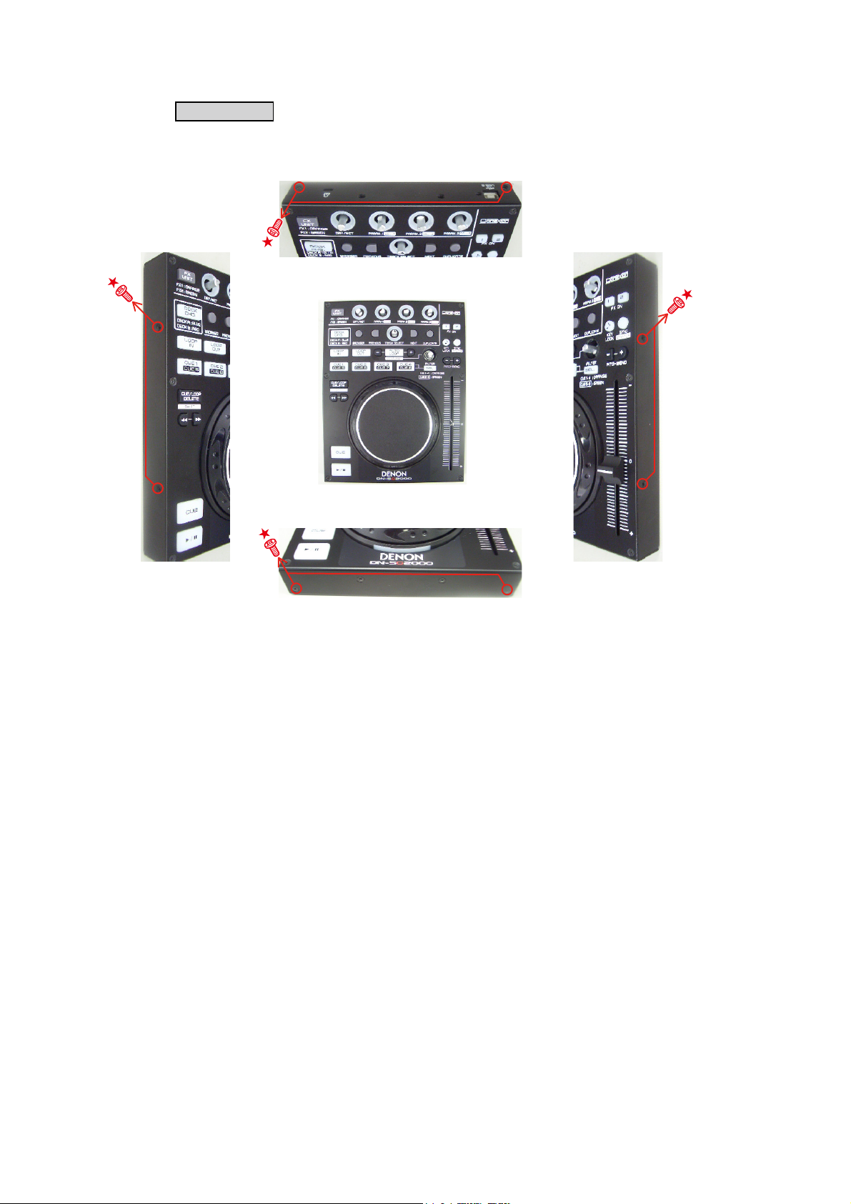
DISASSEMBLY
• Disassemble in order of the arrow of the fi gure of following fl ow.
• In the case of the re-assembling, assemble it in order of the reverse of the following fl ow.
• In the case of the re-assembling, observe "attention of assembling" it.
• If wire bundles are untied or moved to perform adjustment or parts replacement etc., be sure to rearrange them neatly
as they were originally bundled or placed afterward.
Otherwise, incorrect arrangement can be a cause of noise generation.
TOP PANEL
Refer to "DISASSEMBLY
1. TOP PANEL"
and "EXPLODED VIEW"
INNER PANEL
Refer to "DISASSEMBLY
2. INNER PANEL"
and "EXPLODED VIEW"
CONTROL PCB ASS'Y
Refer to "DISASSEMBLY
3. CONTROL PCB ASS'Y
and "EXPLODED VIEW"
CONTROL PCB ASS'Y
(Ref. No. of EXPLODED VIEW : 3)
RUBBER BUTTON
Refer to "DISASSEMBLY
and "EXPLODED VIEW"
SENSOR PCB ASS'Y
(Ref. No. of EXPLODED VIEW : 4)
WHEEL ASS'Y
Refer to "DISASSEMBLY
4. WHEEL ASS'Y"
and "EXPLODED VIEW"
About the photos used for descriptions in the DISASSEMBLY" section.
• The direction from which the photographs used herein were photographed is indicated at "Direction of photograph: ***"
at the left of the respective photographs.
• Refer to the table below for a description of the direction in which the photos were taken.
• Photographs for which no direction is indicated were taken from above the product.
The viewpoint of each photograph
(Photografy direction)
[View from above]
Direction of photograph: B
Front side
Direction of photograph: C
Direction of photograph: D
Direction of photograph: A
5
Page 6
1. TOP PANEL
(1) Remove the screws.
TOP PANELProceeding :
Direction of photograph: B
Direction of
photograph: C
Direction of
photograph: D
Direction of photograph: A
6
Page 7
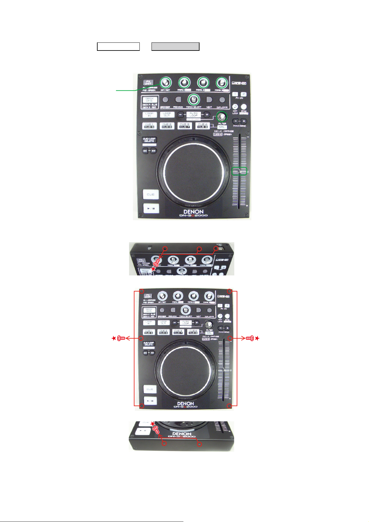
2. INNER PANEL
TOP PANELProceeding :
(1) Remove the knobs.
KNOB
INNER PANEL
→
(2) Remove the screws.
Direction of photograph: B
Direction of photograph: A
7
Page 8
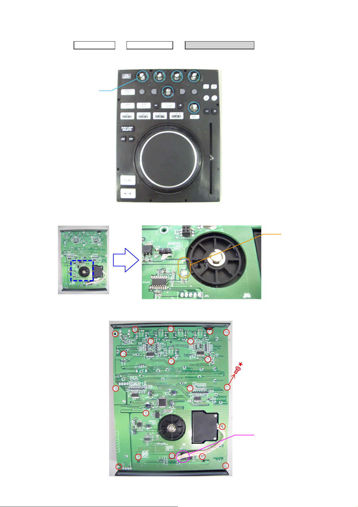
3. CONTROL PCB ASS'Y
TOP PANELProceeding :
(1) Remove the Nuts.
(2) Remove the solder.
NUT
INNER PANEL
→
CONTROL PCB ASS'Y
→
(3) Disconnect the connector wire, then remove the screws.
Solder
CN102
8
Page 9
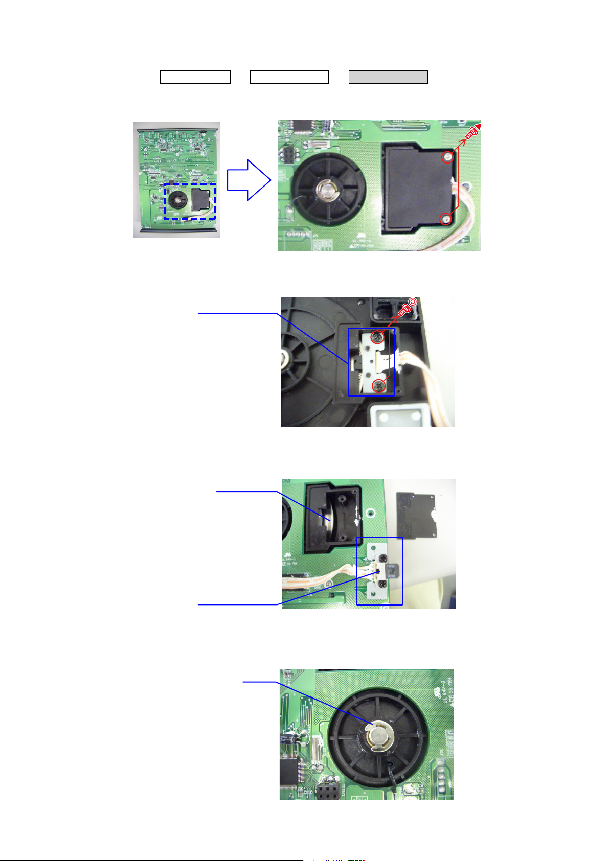
4. WHEEL ASS'Y
TOP PANELProceeding :
(1) Remove the screws.
(2) Remove the screws.
INNER PANEL
→
SENSOR PCB ASS'Y
WHEEL ASS'Y
→
(3) Remove the SENSOR PCB ASS'Y.
Note:
(4) Remove the E RING.
Note:
Donotcomeoutofthebearingwhenyoutransformashaft.
DonotdamagetheWHEELPLATE.
WHEEL PLATE
SENSOR PCB ASS'Y
Donotholddownthecircumferenceoftheshaftwithatool.
E RING
9
Page 10
SPECIAL MODE
1. Special mode setting
Connect to PC while pressing buttons A, B and C.
Mode A B C
Version Up Mode 1 2 3 Firmware Upgrade
Version Display 1 3 4 Firmware version display
Test Mode 1 2 4 LED(Button) Check
1 2 3 4
Contents
2. Version Up Mode
(1) Pressing (SHIFT+NEXT+PREVIOUS) at the same time, then connect SC2000 to PC for F/W version processing.
(2) DN-SC2000 will enter updating mold. CUE-1 will light to indicate “Update Ready.”
(3) PC Operation System will pop-up a new hard disc, named DN-SC2000.
(4) Copy updated fi le (EX: DN-SC2000_v1.13.bin), and paste on “DN-SC2000” hard disc.
(5) It will start updating. After updating successfully, DN-SC2000 will switch to Midi Controller automatically.
(6) Firmware updating State
CUE-1: Update Ready, CUE-2: Update Data(0%), CUE-3: Update Data(50%), CUE-4: Update Data(100%)
FX UNIT: Update Success (* If it doesn’t light, it means “Updating Error”)
(7) Upon completion of the upgrade, it automatically restarts, start in Normal mode.
Upgrade will end in about 10 seconds.
Note:
Please do not switch off the PC during update of Firmware. In addition, please do not take off a USB cable.
10
Page 11

3. Version Display
Press (SHIFT+NEXT+SYNC) at the same time, then connect SC2000 to PC to check the light buttons that represent F/W
version.
Press (Shift) to retrurn to Normal Mode.
How to read the version number
Firmware Version Leds (Ver X .YZ)
X:The first digit numeric display.
1
234
1
2
1
34
2
3
4
56 7 8 9
For example, Ver 1.13
DRY/WET(1) knob
FX ON 1(1) button
DECK CHG.(1), LOOP IN(2), LOOP OUT(3) button
Five places of LED turns on
Y:The second digit numeric display.
Z:The third digit numeric display.
11
Page 12

4. Test Mode
(1) Press ing (SHIFT+PREVIOUS+SYNC) at the same time, then connect SC2000 to PC to start Test Moe.
(2) When you enter the test mode LED lights. The combination of LED A and B in two ways for each combination,
→i are lit and blinking patterns.
q
A pattern lit
q
A pattern blink
e
(A pattern of fl ashing lights part)
A pattern dimmer
t
B pattern lit
w
B pattern blink
r
B pattern of fl ashing lights part
(
B pattern dimmer
y
)
A pattern dimmer blink
u
(A dimmer part fl ashing)
(3) (PREVIOUS) button is pressed, the above
Recconnect SC2000 to PC to retrurn to Normal Mode.
q
B pattern dimmer blink
i
(B dimmer part fl ashing)
→i repeat the pattern.
12
Page 13

ABOUT REPLACE THE MICROPROCESSOR WITH A NEW ONE
When replaced of the U-PRO (Microprocessor) or the Flash ROM, confi rm contents of the following.
PWB Name Ref. No. Description
MAIN IC101 MC9S08JM32CLH B P/N : 941243004230P
After replaced
A : Mask ROM (With software). No need write-in of software to the microprocessor.
B : Flash ROM (With software). Usually, no need write-in of software. But, when the software was updated, you should be
write-in of the new software to the microprocessor or fl ash ROM. Please check the software version.
C : Empty Flash ROM (Without software). You should be write-in of the software to the microprocessor or fl ash ROM.
Refer to "Update procedure" or "writing procedure", when you should be write-in the software.
Refer to "SPECIAL MODE : 2.Version Up Mode" for the procedure of the fi rmware update.
b
After
replaced
Remark
13
Page 14

TROUBLE SHOOTING
FLOW CHART NO.1 (MAIN UNIT)
The power cannot be turned on.
YES
Is the USB cable or the USB terminal of the PC side normal?
YES
Check JK101 and the periphery circuit, and replace it if defective.
FLOW CHART No.2 (MAIN UNIT)
+3.3V is not outputted.
YES
Is the +5V line voltage normal?
YES
Check JK101 and the periphery circuit, and replace it if defective.
FLOW CHART No.3 (MAIN UNIT)
NO
NO
Reconnect normally.
Refer to FLOW CHART NO.1 [The
power cannot be turned on.]
The key operation is not functioning.
YES
Are the contact point and the installation state of the key
switches(SW101~SW134) normal?
YES
Does LED (D153A~D183A/D153B~D183B) light correctly ?
YES
When pressing each key switches, do the voltage of each pin of
IC101(shown below) decrease?
SW133, SW125, SW119, SW113, SW107, SW101 : IC101 61 pin
SW134, SW126, SW120, SW114, SW108, SW102 : IC101 1 pin
SW131, SW127, SW121, SW115, SW109, SW103 : IC101 63 pin
SW132, SW122, SW116, SW110, SW104 : IC101 64 pin
SW129, SW123, SW117, SW111, SW105 : IC101 62 pin
SW130, SW124, SW118, SW112, SW106 : IC101 60 pin
YES
NO
NO
NO
Re-install the switches
(SW101~SW134)
Check Q105~Q108 and the periphery
circuit,and replace it if defective.
Check the key switches
(SW101~SW134) and their periphery,
and service it if detective
Replace IC101.
14
Page 15

FLOW CHART No.4 (MAIN UNIT)
The key operation is not Touch sence functioning.
YES
Are the contact point and the installation state of the JOG Wheel
Top panel normal?
YES
Is signal output from IC104 pin No.5?
Doesn't Touch : 0V / Touch : 5V
YES
Replace IC101.
NO
Replace the JOG wheel.
NO
Replace IC104
15
Page 16

BLOCK DIAGRAM
KEY
LED
PIC16F616
WHEEL
(P.I.)
74595
LED DRIVER
MC9S08JM32
MCU
USB JACK
2
3 1
PITCH VR
ENCODER
1 2
16
Page 17

17
CONTROL UNIT (COMPONENT SIDE) SENSOR UNIT (COMPONENT SIDE)
鉛フリー半田
半田付けには、鉛フリー半田 (Sn-Ag-Cu) を使用してください。
Lead-free Solder
When soldering, use the Lead-free Solder (Sn-Ag-Cu).
987654321
L
K
J
I
H
G
F
E
D
C
B
A
PRINTED WIRING BOARDS
21
A
B
Page 18

18
CONTROL UNIT (FOIL SIDE)
鉛フリー半田
半田付けには、鉛フリー半田 (Sn-Ag-Cu) を使用してください。
Lead-free Solder
When soldering, use the Lead-free Solder (Sn-Ag-Cu).
123454789
L
K
J
I
H
G
F
E
D
C
B
A
Page 19

19
DB5
DB3
DB2
DB1
KR5
KR4
DB0
D156A
CUE1/5
Q11Q22Q33Q44Q55Q66Q77GND
8
DSO
9
MR
10
SHCP
11
STCP
12
OE13DS
14
Q0
15
VCC
16
IC105
74595
R113A
270
C122
0.1
D154A
CUE
D155A
CUE1/5
/OE
STCP
SHCP
DS
C109
0.1
C110
0.1
C126
100/10
R107
1M
X101
12M
C112
33P
C113
33P
R108
10K
C107
0.1
R106
0
L103
10uH
R105
NC
R104
NC
C111
100/10
BKGD
1 2
3 4
5 6
CN101
HEADER 3X2(LPP->NC)
/URST
AD
R114A
110
R115A
110
DB4
SW113
FAST SEARCH-
SW114
LOOP OUT
SW115
PREVIOUS
SW116
+
SW107
PLAY
SW108
DELETE/SHIFT
SW109
SW110
AUTO LOOP
SW111
SEL
SW112
KEY LOCK
SW101
CUE
SW102
FAST SEARCH+
SW103
CUE2/6
D
SW117
CUE4/8
SW118
PITCH+
VBUS
SW104
CUE3/7
SW105
PITCH-
Q11Q22Q33Q44Q55Q66Q77GND
8
DSO
9
MR
10
SHCP
11
STCP
12
OE13DS
14
Q0
15
VCC
16
IC106
74595
R117A
110
C123
0.1
/OE
STCP
SHCP
D158A
CUE2/6
R116A
110
D157A
CUE2/6
C106
0.47
C105
4.7/10
R102
30
R101
30
CHASSIS
PTC4
1
IRQ/TPMCLK
2
RESET
3
PTF0/TPM1CH2
4
PTF1/TPM1CH3
5
PTF2/TPM1CH4
6
PTF3/TPM1CH5
7
PTF4/TPM2CH0
8
PTC6
9
PTF7
10
PTF5/TPM2CH1
11
PIF6
12
PTE0/TxD1
13
PTE1/RxD1
14
PTE2/TPM1CH0
15
PTE3/TPM1CH1
16
PTE4/MISO117PTE5/MOSI118PTE6/SPSCK119PTE7/SS120VDD21VSS22USBDN23USBDP24VUSB3325PTG0/KBIP026PTG1/KBIP127PTA028PTA129PTA230PTA331PTA4
32
PTA5
33
PTB0/MISO2/ADP0
34
PTB1/MOSI2/ADP1
35
PTB2/SPSCK2/ADP2
36
PTB3/SS2/ADP3
37
PTB4/KBIP4/ADP4
38
PTB5/KBIP5/ADP5
39
PTB6/ADP6
40
PTB7/ADP7
41
PTD0/ADP8/ACMP+
42
PTD1/ADP9/ACMP–
43
VDDAD
44
VREFH
45
VREFL
46
VSSAD
47
PTD2/KBIP2/ACMPO
48
PTD3/KBIP3/ADP10
49
PTD4/ADP11
50
PTD551PTD652PTD7
53
PTG2/KBIP654PTG3/KBIP7
55
BKGD/MS
56
PTG4/XTAL
57
PTG5/EXTAL
58
VSSOSC
59
PTC0/SCL
60
PTC1/SDA
61
PTC2
62
PTC3/TxD263PTC5/RxD2
64
IC101
MC9S08JM32
1
2 3
4
L101
ACM2012
L102
BEAD
C102
0.1
C101
10/16
KR3
KR2
SW125
FX UNIT
SW126
DECK CHG.
SW119
CUE1/5
SW120
LOOP IN
SW121
BROWSER
SW122
NEXT
SW123
DUPLICATE
SW124
FX ON1
KR1
KR0
SW106
SYNC
EN2B
EN2A
C1300.01
C1290.01
1234
5
SW130
FIL TER
D172A
PRA2
Q11Q22Q33Q44Q55Q66Q77GND
8
DSO
9
MR
10
SHCP
11
STCP
12
OE13DS
14
Q0
15
VCC
16
IC107
74595
R129A
270
C124
0.1
D170A
TRACK SEL.
D171A
PRA2
/OE
STCP
SHCP
R130A
110
R131A
110
D172B
PRA2
D170B
TRACK SEL.
D171B
PRA2
D156B
CUE1/5
D154B
CUE
D155B
CUE1/5
D158B
CUE2/6
D157B
CUE2/6
3.3V
C103
10/16
IGO
IC103
BA33T
C104
0.1
VBUS
R113B
270
R114B
110
R115B
110
R129B
270
R130B
110
R131B
110
R116B
110
R117B
110
DB5
DB0
DB4
DB2
DB3
DB1
EN2A
EN6A
STCPDSSHCP
/OE
R103
10K
C108 0.1
D101
EDZC6.8B
D102
EDZC6.8B
D103
EDZC6.8B
D104
EDZC6.8B
C114
2.2/50
NC
1
SUB
2
GND
3
VO
4
VCC
5
IC102
BD4740G
R110
10K
Q102
C114ES
Q104
C114ES
Q103
C114ES
Q105
C114ES
Q106
C114ES
Q118
C114ES
Q119
C114ES
Q120
C114ES
R146
100
R147
100
R148
100
R149
100
D152
SMAJ-6.0A
D141
1SS355
D142
1SS355
D143
1SS355
D144
1SS355
R109
10K(LPP->0)
D111
1SS355
D105
1SS355
D117
1SS355
D123
1SS355
D129
1SS355
D135
1SS355
D106
1SS355
D112
1SS355
D118
1SS355
D124
1SS355
D130
1SS355
D136
1SS355
D107
1SS355
D113
1SS355
D119
1SS355
D125
1SS355
D131
1SS355
D132
1SS355
D126
1SS355
D120
1SS355
D114
1SS355
D108
1SS355
D133
1SS355
D127
1SS355
D121
1SS355
D115
1SS355
D109
1SS355
D128
1SS355
D122
1SS355
D116
1SS355
D110
1SS355
D134
1SS355
Q11Q22Q33Q44Q55Q66Q77GND
8
DSO
9
MR
10
SHCP
11
STCP
12
OE13DS
14
Q0
15
VCC
16
IC108
74595
C125
0.1
/OE
STCP
SHCP
DSO
DSO
DSO
DSO
D174A
PRA3
R132A
110
R133A
110
D174B
PRA3
D173B
PRA3
R132B
110
R133B
110
Q121
C114ES
Q122
C114ES
D173A
PRA3
VCC
1
RA5
2
RA4
3
RA3
4
RC5
5
RC4
6
RC37RC2
8
RC1
9
RC0
10
RA2
11
RA1
12
RA0
13
GND
14
IC104
PIC16F616
C1
0.1
R1
2.4K
R2
1K
R5
20K
R7
51K
C3
1u/16V
WHEEL
WHEEL
1
2
3
4
5
JP1
IC
MCLR
VBUS
ISCPDAT
ICSPCLK
DGND
WHEEL
D
VBUS
C8
1/16
IN
1
2
3
4
CN102
4P
VBUS
JW2
JW1
CHB
1
VCC
2
CHA
3
GND
4
M301
WHEEL ENCODER
1
2
3
4
W102
4P
D166A
DRY/WET
R119A
110
R123A
270
R122A
330
R121A
110
R120A
110
D161A
LOOP OUT
D162A
LOOP IN
D163A
DECK CHG.
D164A
DECK CHG.
D165A
DRY/WET
D160A
CUE3/7
R118A
110
R124A
110
R125A
110
D159A
CUE3/7
R127A
110
D168A
PRA1
R126A
110
D167A
PRA1
D182A
SYNC
R135A
110
R139A
110
R138A
110
R137A
110
R136A
270
D177A
AUTO LOOP
D178A
CUE4/8
D179A
FX UNIT
D180A
FX UNIT
D181A
KEY LOOK
D176A
FX ON2
R134A
110
R140A
110
R141A
330
D175A
FX ON1
D177B
AUTO LOOP
D179B
FX UNIT
D180B
FX UNIT
D166B
DRY/WET
D161B
LOOP OUT
D162B
LOOP IN
D165B
DRY/WET
D160B
CUE3/7
D159B
CUE3/7
D168B
PRA1
D167B
PRA1
R118B
110
R119B
110
R120B
110
R121B
110
R124B
110
R125B
110
R136B
270
R138B
110
R139B
110
R126B
110
R127B
110
Q107
C114ES
Q108
C114ES
Q109
C114ES
Q110
C114ES
Q111
C114ES
Q112
C114ES
Q114
C114ES
Q113
C114ES
Q115
C114ES
Q116
C114ES
Q123
C114ES
Q124
C114ES
Q125
C114ES
Q126
C114ES
Q127
C114ES
Q128
C114ES
Q129
C114ES
Q130
C114ES
R151
100
R152
100
R154
100
D146
1SS355
D147
1SS355
D149
1SS355
R150
100
D145
1SS355
R153
100
D148
1SS355
R145
100
D140
1SS355
LED1
LED2
LED3
LED4
LED5
LED6
LED7
LED8
LED9
LED10
LED11
LED12
LED13
LED14
LED15
LED16
LED17
LED18
LED19
LED20
LED21
LED22
LED23
LED24
LED25
LED26
LED27
LED28
LED29
LED30
VB
1
D-
2
D+
3
DGND
4
CHASSIS
5
CHASSIS
6
JK101
MIDI USB(B Type)
R112A
110
D153A
PLAY
R128A
330
D169A
TRACK SEL.
D169B
TRACK SEL.
D153B
PLAY
R112B
110
R128B
330
Q101
C114ES
Q117
C114ES
R144
100
D139
1SS355
LED1
LED2
LED3
LED4
LED5
LED6
LED7
LED8
LED9
LED10
LED11
LED12
LED13
LED14
LED15
LED16
LED17
LED18
LED19
LED20
LED21
LED22
LED23
LED24
LED25
LED26
LED27
LED28
LED29
LED30
R111
10K
A3A1
A2A4
B3B1
B2B4
VR101
10KBX2
PITCH
AD5V
C115
3300P
C116
3300P
AD VR0
AD VR1
JW1
JW2
KR0
KR1
KR2
KR3
KR4
AD VR1
AD VR0
WHEEL
KR5
3.3V
CLED1
CLED2
CLED3
CLED4
CLED9
CLED10
CLED11
CLED5
CLED8
CLED7
CLED6
CLED1
CLED2
CLED3
CLED4
CLED5
CLED6
CLED7
CLED8
CLED9
CLED10
CLED11
VBUS
EN1B
EN1A
C1280.01
C1270.01
1234
5
SW129
TRACK SEL.
EN4B
EN4A
C138 0.01
C137 0.01
1234
5
SW134
PRA1
EN3B
EN3A
C1360.01
C1350.01
1234
5
SW133
DRY/WET
EN6B
EN6A
C134 0.01
C133 0.01
1234
5
SW132
PRA3
EN5B
EN5A
C132 0.01
C131 0.01
1234
5
SW131
PRA2
EN5A
EN1A
EN4A
EN3A
EN4B
EN3B EN1B
EN2B
EN5B
EN6B
405-HDJ9800-1020
R143A
330
D184A
JOG WHEEL
D184B
JOG WHEEL
R143B
330
Q132
C114ES
R155A
270
D186A
JOG WHEEL
D186B
JOG WHEEL
R155B
270
Q134
C114ES
JOG WHEEL LED1
JOG WHEEL LED2
JOG WHEEL LED1
JOG WHEEL LED2
R142A
110
D183A
CUE4/8
D183B
CUE4/8
R142B
110
Q131
C114ES
LED31
LED31
D137
1SS355
SW127
FX ON2
R123B
270
R122B
330
D163B
DECK CHG.
D164B
DECK CHG.
R137B
110
D178B
CUE4/8
R134B
110
D175B
FX ON1
R135B
110
D176B
FX ON2
D182B
SYNC
D181B
KEY LOOK
R140B
110
R141B
330
D150
EDZC6.8B
FU1 1A
EN2B
EN2A
EN1B
EN1A
EN4B
EN4A
EN3B
EN3A
EN6B
EN6A
EN5B
EN5A
R158
5.6K
R156
5.6K
R166
5.6K
R164
5.6K
R162
5.6K
R160
5.6K
R159
5.6K
R157
5.6K
R167
5.6K
R165
5.6K
R163
5.6K
R161
5.6K
GND POWER + POWER -
87654321
A
B
C
D
E
F
SCHEMATIC DIAGRAMS (1/1)
Page 20

Grease:
Product name : RS Paste
Maker : DAIZO corporation(Nichimoly)
Parts marked with this symbol have critical
characteristics.
Use ONLY replacement parts recommended by
the manufacturer.
WARNING:
EXPLODED VIEW & POINTS OF
GREASING
20
Page 21

PARTS LIST OF EXPLODED VIEW
zParts for which "nsp" is indicated on this table cannot be supplied.
z
P.W.B. ASS'Y for which "nsp" is indicated on this table cannot be supplied. When repairing the P.W.B. ASS'Y, check the board parts table and order replacement parts.
zPart indicated with the mark " ★ " is not illustrated in the exploded view.
zThe parts listed below are for maintenance only, might differ from the parts used in the unit in appearances or dimensions.
Note: The symbols in the column "Remarks" indicate the following destinations.
E3 : U.S.A. & Canada model E2 : Europe model EA : Australia model
Ref. No. Part No. Part Name Remarks Q'ty New
1 nsp FRAME COVER ASS'Y 701-2000-4921 1
1-1 941443004100P FRAME PLASTIC ASS'Y 701-2000-4816 1 *
1-2 nsp JACKET COVER 100-2000-2775 1
1-3 nsp PULLEY SPRING 603-PROS2-256A 1
2 nsp WHEEL ASS'Y 701-2000-4922 1
2-1 941412004120P WHEEL & PLATE ASS'Y 701-2000-4815 1 *
2-1-1 nsp WHEEL & SHAFT ASS'Y 701-2000-4815 1
2-1-2 nsp WHEEL PLATE 300-2000-1833 1
2-1-3 nsp SPRING(SUS304,Φ0.3,L=6) 603-M1-384 1
2-1-4 nsp SCWER(SAE1018,STS,2.0*3) 602-STS2003-677 1
2-2 941483004110P ENCODER PLATE 300-PROS2-848 1 *
2-3 nsp ENCODER FIXED PLATE 300-PROS2-851 1
2-4 nsp SCREW(PTBΦ2*L6) 602-PROS2-363 6
3 nsp CONTROL PCB ASS'Y 704-SC2000-9495 1
4 nsp SENSOR PCB ASS'Y 704-CDI600-7990 1
5 nsp PUSH BUTTON 100-700-2679 1
6 nsp JOG TUNING KNOB 100-1000S-2736 6
7 941483004110P JACKET RING 100-2000-2774 5 *
8 nsp SENSOR FIXED PLATE(SECC,1.2t) 300-HDJ9800-981 1
9 941402004030P TOP COVER 300-2000-1830 1 *
10 nsp BASE 300-2000-1831 1
11 nsp USB CABLE(L=1000mm) 408-IM-081 1
12 nsp DUST-PROOF SLICE 501-HDJ9800-1648 1
13 941411003840P SOFT KNOB 604-2000-549 1 *
14 941411003850P 6 KEY SOFT KNOB 604-2000-550 1 *
15 941411003860P 2 KEY SOFT KNOB 604-2000-551 1 *
16 nsp PULLEY WASHER(Φ1.6*6*0.25t) 606-F200-003 1
17 nsp E RING 606-DJ3000-105 1
18 nsp F00T(PORON,BLACK,Φ15*3t) 612-HV3500K-055 4
19 nsp FIBROUS(Φ4.6*6.2*0.3t) 612-1000S-348 1
20 nsp SCREW(SAE1018,PTP,M2.6*L8) 602-SL24F-099 20
21 nsp SCREW(Φ5,L=8) 602-HP1010K-182 18
22 nsp SCREW(SAE1018,ISOP,M3*5L*P0.5) 602-MP3-324 2
23 nsp SCREW(PTBΦ2*L6) 602-PROS2-363 2
24 nsp SCREW(SAE1018,PTBΦ3*L8) 602-DJ5500-452 2
25 nsp SCREW(C1018,ISOF,M2*5) 602-ISOF2005-686B 1
26-1 nsp BAR CODE-MAKE DATE(24*8mm,t=0.1mm) 701-SC2000-4916 1
26-2 nsp BAR CODE-SERIAL NO.(46*8mm,t=0.1mm)
21
Page 22

PACKING VIEW
6
5
2
4
7
8
3
8
PARTS LIST OF PACKING & ACCESSORIES
zParts for which "nsp" is indicated on this table cannot be supplied.
zPart indicated with the mark " ★ " is not illustrated in the exploded view.
zThe parts listed below are for maintenance only, might differ from the parts used in the unit in appearances or dimensions.
Note: The symbols in the column "Remarks" indicate the following destinations.
Note: The symbols in the column "Remarks" indicate the following destinations.
E3 : U.S.A. & Canada model E2 : Europe model EA : Australia model
Ref. No. Part No. Part Name Remarks Q'ty New
1 941533004050P POLYFOAM D 506-2000-589D 1 *
2 941533004060P POLYFOAM U 506-2000-589U 1 *
3 941535004070P SOFT BAG 509-2000-284 1 *
4 nsp USB CABLE(L=1000mm) 408-IM-081 1
4 nsp POLYBAG(120*250mm) 505-HM500A-049 1
5 941541004080P I/B 502-DSC2000-3008 1 *
5 941543004250P QUICK GUIDE 502-DSC2000-3019 1 *
6 941531004090S GIFT BOX 507-SC2000-3206 1 *
7 nsp BAR CODE(86'*209mm,t=0.1mm) 701-SC2000EM-4916 1
7-1 - BAR CODE-SERIAL NO.(FOR GIFT BOX) - -
7-2 - BAR CODE-SERIAL NO.(FOR OUT CARTON) - -
22
Page 23

SEMICONDUCTORS
PTF2/TPM1CH4
1
2
3
4
5
6
7
8
RESET
PTF0/TPM1CH2
PTF3/TPM1CH5
PTF4/TPM2CH0
PTC6
PTF7
V
USB33
USBDP
USBDN
V
SS
V
DD
PTE7/SS1
PTE6/SPSCK1
PTB7/ADP7
PTD0/ADP8/ACMP+
PTD1/ADP9/ACMP–
V
DDAD
V
REFH
PTB1/MOSI2/ADP1
PTB6/ADP6
PTD5
PTG2/KBIP6
PTC5/RxD2
PTG4/XTAL
BKGD/MS
PTG3/KBIP7
PTD2/KBIP2/ACMPO
PTD6
PTD7
43
42
41
40
39
38
18 19 20 21 22
23
505152535455
17
32
33
49
48
64
9
PTF5/TPM2CH1
10
PTF6
11
PTE0/TxD1
16
PTE3/TPM1CH1
PTG0/KBIP024PTG1/KBIP1
25
PTA0
26
PTA1
27
PTB5/KBIP5/ADP5
37
PTB4/KBIP4/ADP4
36
PTB3/SS2/ADP3
35
PTB2/SPSCK2/ADP2
34
PTG5/EXTAL
56
V
SSOSC
57
PTC0/SCL
58
PTC1/SDA
59
PTF1/TPM1CH3
12
PTE1/RxD1
13
14
15
PTE2/TPM1CH0
PTA2
28 29 30 31
V
REFL
44
45
46
V
SSAD
47
PTC3/TxD2
63 62 61
PTC2
60
PTC4
IRQ/TPMCLK
PTE4/MISO1
PTE5/MOSI1
PTA3
PTA4
PTB0/MISO2/ADP0
PTA5
PTD4/ADP11
PTD3/KBIP3/ADP10
64-Pin QFP/LQFP
Only major semiconductors are shown, general semiconductors etc. are omitted to list.
The semiconductor which described a detailed drawing in a schematic diagram are omitted to list.
1. IC's
MC9S08JM32 (IC101)
23
Page 24

MC9S08JM32 Block Diagram
PTD4/ADP11
PTD5
PTD6
PTC1/SDA
PTC0/SCL
V
SS
V
DD
PTE3/TPM1CH1
PTE2/TPM1CH0
PTA5– PTA0
PTE0/TxD1
PTE1/RxD1
PTD1/ADP9/ACMP–
PTD0/ADP8/ACMP+
PTC6
PTC5/RxD2
PTC4
PTC3/TxD2
PTC2
PORT A
PORT C
PORT D
PORT E
8-BIT KEYBOARD
INTERRUPT MODULE (KBI)
IIC MODULE (IIC)
8-/16-BIT SERIAL PERIPHERAL
INTERFACE MODULE (SPI1)
USER Flash (IN BYTES)
USER RAM (IN BYTES)
ON-CHIP ICE AND
DEBUG MODULE (DBG)
MC9S08JM60 = 60,912
HCS08 CORE
CPUBDC
NOTES:
1. Port pins are software configurable with pullup device if input port.
2. Pin contains software configurable pullup/pull-down device if IRQ is enabled
(IRQPE = 1). Pull-down is enabled if rising edge detect is selected (IRQEDG = 1)
3. IRQ does not have a clamp diode to V
DD
. IRQ must not be driven above VDD.
4. Pin contains integrated pullup device.
5. When pin functions as KBI (KBIPEn = 1) and associated pin is configured to enable the
pullup device, KBEDGn can be used to reconfigure the pullup as a pull-down device.
2-CHANNEL TIMER/PWM
MODULE (TPM2)
PTB5/KBIP5/ADP5
PORT B
PTE5/MOSI1
PTE4/MISO1
PTE6/SPSCK1
PTE7/SS1
HCS08 SYSTEM CONTROL
RESETS AND INTERRUPTS
MODES OF OPERATION
POWER MANAGEMENT
VOLTAGE
REGULATOR
COP IRQ LVD
LOW-POWER OSCILLATOR
MULTI-PURPOSE CLOCK
GENERATOR (MCG)
RESET
V
SSAD
V
DDAD
V
REFH
ANALOG-TO-DIGITAL
CONVERTER (ADC)
6-CHANNEL TIMER/PWM
MODULE (TPM1)
PTD7
6
PTB4/KBIP4/ADP4
PTG3/KBIP7
PTG2/KBIP6
PORT G
12-CHANNEL, 12-BIT
BKGD/MS
PTF3/TPM1CH5
PTF2/TPM1CH4
PTF0/TPM1CH2
PTF1/TPM1CH3
PORT F
PTF5/TPM2CH1
PTF4/TPM2CH0
PTF6
PTF7
INTERFACE MODULE (SCI1)
SERIAL COMMUNICATIONS
INTERFACE MODULE (SCI2)
SERIAL COMMUNICATIONS
PTG0/KBIP0
PTG1/KBIP1
MC9S08JM32 = 32,768
V
REFL
PTG4/XTAL
PTG5/EXTAL
IRQ/TPMCLK
RxD2
TxD2
SDA
SCL
8
KBIPx
KBIPx
TPMCLK
SPSCK1
SS1
MISO1
MOSI1
TPMCLK
TPM1CH1
TPM1CH0
RxD1
TxD1
EXTAL
XTAL
4
4
USB SIE
USB ENDPOINT
RAM
FULL SPEED
USB
TRANSCEIVER
USBDP
USBDN
MISO2
SS2
SPSCK2
MOSI2
PTB1/MOSI2/ADP1
PTB0/MISO2/ADP0
PTB7/ADP7
PTB6/ADP6
8-/16-BIT SERIAL PERIPHERAL
INTERFACE MODULE (SPI2)
REAL-TIME COUNTER
(RTC)
PTB3/SS2/ADP3
PTB2/SPSCK2/ADP2
TPM1CHx
4
TPM2CH1
TPM2CH0
4
ANALOG COMPARATOR
(ACMP)
SYSTEM
USB 3.3-V VOLTAGE REGULATOR
V
USB33
MC9S08JM60 = 4096
MC9S08JM32 = 2048
ACMPO
ACMP+
ACMP–
PTD3/KBIP3/ADP10
PTD2/KBIP2/ACMPO
V
SSOSC
24
Page 25

MC9S08JM32 Device Pin Assignment
No Name Symbol I/O Function
1 PTC4 PTC4 O Port C I/O
2 IRQ/TPMCLK NC NC External Interrupt Pin
3 RESET RESET Development system can directly reset the MCU system
4 PTF0/TPM1CH2 PTF0 I Port F I/O
5 PTF1/TPM1CH3 PTF1 I Port F I/O
6 PTF2/TPM1CH4 PTF2 I Port F I/O
7 PTF3/TPM1CH5 PTF3 I Port F I/O
8 PTF4/TPM2CH0 PTF4 I Port F I/O
9 PTC6 NC NC Port C I/O
10 PTF7 PTF7 O Port F I/O
11 PTF5/TPM2CH1 PTF5 I Port F I/O
12 PTF6 PTF6 O Port F I/O
13 PTE0/TxD1 NC NC Port E I/O
14 PTE1/RxD1 NC NC Port E I/O
15 PTE2/TPM1CH0 TPM1CH0 I TIMER/PWM MODULE (TPM1)
16 PTE3/TPM1CH1 TPM1CH1 I TIMER/PWM MODULE (TPM1)
17 PTE4/MISO1 PTE4 O Port E I/O
18 PTE5/MOSI1 PTE5 O Port E I/O
19 PTE6/SPSCK1 PTE6 O Port E I/O
20 PTE7/SS1 PTE7 O Port E I/O
21 VDD VDD The primary power supply pins for the MCU
22 VSS VSS The primary power supply pins for the MCU
23 USBDN USBDN I/O Differential USB signaling
24 USBDP USBDP I/O Differential USB signaling
25 VUSB33 VUSB33 3.3V USB voltage regulator output or 3.3V USB transceiver/resistor
26 PTG0/KBIP0 PTG0 I Port G I/O
27 PTG1/KBIP1 PTG1 I Port G I/O
28 PTA0 PTA0 O Port A I/O
29 PTA1 PTA1 O Port A I/O
30 PTA2 PTA2 O Port A I/O
31 PTA3 PTA3 O Port A I/O
32 PTA4 PTA4 O Port A I/O
33 PTA5 PTA5 O Port A I/O
34 PTB0/MISO2/ADP0 PTB0 I Port B I/O
35 PTB1/MOSI2/ADP1 PTB1 I Port B I/O
36 PTB2/SPSCK2/ADP2 PTB2 I Port B I/O
37 PTB3/SS2/ADP3 PTB3 I Port B I/O
38 PTB4/KBIP4/ADP4 PTB4 I Port B I/O
39 PTB5/KBIP5/ADP5 PTB5 I Port B I/O
40 PTB6/ADP6 ADP6 I 12-Bit Analog-To-Digital Converter(ADC)
41 PTB7/ADP7 ADP7 I 12-Bit Analog-To-Digital Converter(ADC)
42 PTD0/ADP8/ACMP+ PTD0 I Port D I/O
43 PTD1/ADP9/ACMP– PTD1 I Port D I/O
44 VDDAD VDDAD The analog power supply pins for the MCU
45 VREFH VREFH The voltage reference high inputs respectively for the ADC module
46 VREFL VREFL The voltage reference low inputs respectively for the ADC module
47 VSSAD VSSAD The analog power supply pins for the MCU
48 PTD2/KBIP2/ACMPO PTD2 O Port D I/O
49 PTD3/KBIP3/ADP10 ADP10 I 12-Bit Analog-To-Digital Converter(ADC)
50 PTD4/ADP11 PTD4 O Port D I/O
51 PTD5 PTD5 O Port D I/O
52 PTD6 PTD6 O Port D I/O
25
Page 26

No Name Symbol I/O Function
53 PTD7 PTD7 O Port D I/O
54 PTG2/KBIP6 PTG2 I Port G I/O
55 PTG3/KBIP7 PTG3 I Port G I/O
56 BKGD/MS BKGD Background/Mode Select
57 PTG4/XTAL XTAL External Oscillator
58 PTG5/EXTAL EXTAL External Oscillator
59 VSSOSC VSSOSC Low-Power Oscillator
60 PTC0/SCL PTC0 O Port C I/O
61 PTC1/SDA PTC1 O Port C I/O
62 PTC2 PTC2 O Port C I/O
63 PTC3/TxD2 PTC3 O Port C I/O
64 PTC5/RxD2 PTC5 O Port C I/O
26
Page 27

PIC16F616 (IC104)
RA5/T1CKI/OSC1/CLKIN
RA4/AN3/T1G
/OSC2/CLKOUT
RA3/MCLR
RC5/CCP1/P1A
RC4/C2OUT/P1B
RC3/AN7/C12IN3-/P1C
VDD
/VPP
1
2
3
4
5
6
7
14
13
12
11
10
9
PIC16F616/16HV616
8
VSS
RA0/AN0/C1IN+/ICSPDAT
RA1/AN1/C12IN0-/V
RA2/AN2/T0CKI/INT/C1OUT
RC0/AN4/C2IN+
RC1/AN5/C12IN1-
RC2/AN6/C12IN2-/P1D
REF/ICSPCLK
PIC16F616 Poin Summary
I/O Pin Analog Comparators Timer CCP Interrupts Pull-ups Basic
RA0 13 AN0 C1IN+ — — IOC Y ICSPDAT
RA1 12 AN1/V
REF
RA2 11 AN2 C1OUT T0CKI — INT/IOC Y —
(1)
RA3
4— — — — IOCY
RA4 3 AN3 — T1G — IOC Y OSC2/CLKOUT
RA5 2 — — T1CKI — IOC Y OSC1/CLKIN
RC0 10 AN4 C2IN+ — — — — —
RC1 9 AN5 C12IN1- — — — — —
RC2 8 AN6 C12IN2- — P1D — — —
RC3 7 AN7 C12IN3- — P1C — — —
RC4 6 — C2OUT — P1B — — —
RC5 5 — — — CCP1/P1A — — —
— 1 — — — — — — V
—14 — — — — — — V
Note 1: Input only.
2: Only when pin is configured for external MCLR
C12IN0- — — IOC Y ICSPCLK
(2)
MCLR/V
DD
SS
PP
.
PIC16F616 Device Pin Assignment
Pin No Pin NAME Symbol I/O FUNCTION
1 VDD VBAS POWER
2 RA5 RA5 I Timer1 clock input
3 RA4 RA4 O NC
4 RA3 MCLR I BACKGROUND HEADER
5 RC5 RC5 O PWM output
6 RC4 RC4 O Comparator C2 output
7 RC3 RC3 O NC
8 RC2 RC2 O NC
9 RC1 RC1 O NC
10 RC0 RC0 I Comparator C2 non-inverting input
11 RA2 PA2 O NC
12 RA1 ICSPCLK I Comparators C1 and C2 inverting input/BACKGROUND HEADER
13 RA0 ISCPDAT O BACKGROUND HEADER
14 VSS DGND POWER
27
Page 28

PIC16F616 Block Diagram
OSC1/CLKIN
OSC2/CLKOUT
T1G
Program
Bus
Internal
Oscillator
Block
Configuration
Flash
2K X 14
Program
Memory
14
Instruction Reg
Instruction
Decode &
Control
Timing
Generation
13
Program Counter
Direct Addr
8
Start-up Timer
MCLR
INT
8-Level Stack
(13-Bit)
Power-up
Timer
Oscillator
Power-on
Reset
Watchdog
Timer
Brown-out
Reset
VDD
VSS
RAM Addr
7
Data Bus
RAM
128 Bytes
File
Registers
9
Addr MUX
8
FSR Reg
STATUS Reg
3
8
Shunt Regulator
(PIC16HV616 only)
MUX
ALU
W Reg
Indirect
Addr
8
PORTA
RA0
RA1
RA2
RA3
RA4
RA5
PORTC
RC0
RC1
RC2
RC3
RC4
RC5
T1CKI
T0CKI
Analog-To-Digital Converter
AN4
AN5
AN6
VREF
AN7
Timer0
Comparator Voltage Reference
Absolute Voltage Reference
AN0
AN1
AN2
AN3
Timer1
Timer2
2 Analog Comparators
and Reference
C2IN+
C2OUT
C1OUT
ECCP
C1IN+
C12IN0-
C12IN1-
C12IN2-
C12IN3-
CCP1/P1A
P1B
P1C
P1D
28
Page 29

PARTS LIST OF P.W.B. UNIT
zParts for which "nsp" is indicated on this table cannot be supplied.
zThe parts listed below are for maintenance only, might differ from the parts used in the unit in appearances or dimensions.
Note: The symbols in the column "Remarks" indicate the following destinations.
E3 : U.S.A. & Canada model E2 : Europe model EA : Australia model
CONTROL P.W.B. UNIT ASS'Y
Ref. No. Part No. Part Name Remarks Q'ty New
SEMICONDUCTORS GROUP
IC101 941243004230P
IC102 941239003100S IC(BD4740G-TR,SMP5) 417-9000-740
IC103 00D9587058204 IC(BA033FP-E2,TO-252-3) 417-CTB200-500
IC104 941243004220P IC(PIC16F616-|/SL,SOIC-16) 417-RMP3-936 *
IC105-108 00D9587058709
Q101-132 00D9587057700 TRANSIST0R(DTC114EKAT146,SMT3) 416-HDJ2460-234
Q134 00D9587057700 TRANSIST0R(DTC114EKAT146,SMT3) 416-HDJ2460-234
D101-104 nsp ESD DIODE(EDZCTE616.8B,150MW/,6.93V,EMD2) 414-RMP3-285
D105-137 nsp
D139-149 nsp
D150 nsp ESD DIODE(EDZCTE616.8B,150MW/,6.93V,EMD2) 414-RMP3-285
D152 nsp TVS DIODE(SMAJ6.0A,400W,6.0V,DO-214AC) 414-UDJ200-284
CONTROL IC ASS'Y
(MC9S08JM32CLH,LQFP-64)
IC(74HC595D/74AHC595D/74AHC595DR
/74HC595D@118,SO-16)
SWITCHING DIODE
(ISS355,TE-17,100mA,90V,UMD2)
SWITCHING DIODE
(ISS355,TE-17,100mA,90V,UMD2)
NOTE :
When update Firmware,
please confi rm a last
version in SDI.
Use the service board
after updating it.
704-SC2000-9496 *
417-HDJ9800-643
414-CD1000-075
414-CD1000-075
D169A 941263004170P LED(LTL-1 CHTBK4,3.1Φ,BLUE) 410-CDI600-357 *
D169B 941263004170P LED(LTL-1 CHTBK4,3.1Φ,BLUE) 410-CDI600-357 *
D184A 941263004170P LED(LTL-1 CHTBK4,3.1Φ,BLUE) 410-CDI600-357 *
D184B 941263004170P LED(LTL-1 CHTBK4,3.1Φ,BLUE) 410-CDI600-357 *
D166A 941263004180P LED(YELLOW GREEN,LTL1CHJGDNN) 410-DJ5000-252 *
D166B 941263004180P LED(YELLOW GREEN,LTL1CHJGDNN) 410-DJ5000-252 *
D168A 941263004180P LED(YELLOW GREEN,LTL1CHJGDNN) 410-DJ5000-252 *
D168B 941263004180P LED(YELLOW GREEN,LTL1CHJGDNN) 410-DJ5000-252 *
D172A 941263004180P LED(YELLOW GREEN,LTL1CHJGDNN) 410-DJ5000-252 *
D172B 941263004180P LED(YELLOW GREEN,LTL1CHJGDNN) 410-DJ5000-252 *
D174A 941263004180P LED(YELLOW GREEN,LTL1CHJGDNN) 410-DJ5000-252 *
D174B 941263004180P LED(YELLOW GREEN,LTL1CHJGDNN) 410-DJ5000-252 *
D170A 941263001060S LED(LTL1CHJEDNN,RED) 410-DJ5000-253
D170B 941263001060S LED(LTL1CHJEDNN,RED) 410-DJ5000-253
D186A 941263001060S LED(LTL1CHJEDNN,RED) 410-DJ5000-253
D186B 941263001060S LED(LTL1CHJEDNN,RED) 410-DJ5000-253
D165A 941263004190P LED(LTL1CHJSDNN,YELLOW) 410-HDJ2000-162 *
D165B 941263004190P LED(LTL1CHJSDNN,YELLOW) 410-HDJ2000-162 *
D167A 941263004190P LED(LTL1CHJSDNN,YELLOW) 410-HDJ2000-162 *
D167B 941263004190P LED(LTL1CHJSDNN,YELLOW) 410-HDJ2000-162 *
D171A 941263004190P LED(LTL1CHJSDNN,YELLOW) 410-HDJ2000-162 *
D171B 941263004190P LED(LTL1CHJSDNN,YELLOW) 410-HDJ2000-162 *
D173A 941263004190P LED(LTL1CHJSDNN,YELLOW) 410-HDJ2000-162 *
D173B 941263004190P LED(LTL1CHJSDNN,YELLOW) 410-HDJ2000-162 *
D169A nsp LED HOLDER(LED3-1A-B,H=1.5mm,BLACK) 504-HDJ2000-097 *
D169B nsp LED HOLDER(LED3-1A-B,H=1.5mm,BLACK) 504-HDJ2000-097 *
29
Page 30

Ref. No. Part No. Part Name Remarks Q'ty New
D184A nsp LED HOLDER(LED3-1A-B,H=1.5mm,BLACK) 504-HDJ2000-097 *
D184B nsp LED HOLDER(LED3-1A-B,H=1.5mm,BLACK) 504-HDJ2000-097 *
D170A nsp LED HOLDER(LED3-1A-B,H=1.5mm,BLACK) 504-HDJ2000-097 *
D170B nsp LED HOLDER(LED3-1A-B,H=1.5mm,BLACK) 504-HDJ2000-097 *
D186A nsp LED HOLDER(LED3-1A-B,H=1.5mm,BLACK) 504-HDJ2000-097 *
D186B nsp LED HOLDER(LED3-1A-B,H=1.5mm,BLACK) 504-HDJ2000-097 *
D166A nsp LED HOLDER(LED3-1A-B,H=1.5mm,BLACK) 504-HDJ2000-097 *
D166B nsp LED HOLDER(LED3-1A-B,H=1.5mm,BLACK) 504-HDJ2000-097 *
D168A nsp LED HOLDER(LED3-1A-B,H=1.5mm,BLACK) 504-HDJ2000-097 *
D168B nsp LED HOLDER(LED3-1A-B,H=1.5mm,BLACK) 504-HDJ2000-097 *
D172A nsp LED HOLDER(LED3-1A-B,H=1.5mm,BLACK) 504-HDJ2000-097 *
D172B nsp LED HOLDER(LED3-1A-B,H=1.5mm,BLACK) 504-HDJ2000-097 *
D174A nsp LED HOLDER(LED3-1A-B,H=1.5mm,BLACK) 504-HDJ2000-097 *
D174B nsp LED HOLDER(LED3-1A-B,H=1.5mm,BLACK) 504-HDJ2000-097 *
D165A nsp LED HOLDER(LED3-1A-B,H=1.5mm,BLACK) 504-HDJ2000-097 *
D165B nsp LED HOLDER(LED3-1A-B,H=1.5mm,BLACK) 504-HDJ2000-097 *
D167A nsp LED HOLDER(LED3-1A-B,H=1.5mm,BLACK) 504-HDJ2000-097 *
D167B nsp LED HOLDER(LED3-1A-B,H=1.5mm,BLACK) 504-HDJ2000-097 *
D171A nsp LED HOLDER(LED3-1A-B,H=1.5mm,BLACK) 504-HDJ2000-097 *
D171B nsp LED HOLDER(LED3-1A-B,H=1.5mm,BLACK) 504-HDJ2000-097 *
D173A nsp LED HOLDER(LED3-1A-B,H=1.5mm,BLACK) 504-HDJ2000-097 *
D173B nsp LED HOLDER(LED3-1A-B,H=1.5mm,BLACK) 504-HDJ2000-097 *
D155A 941263002610S CHIP LED(YELLOW,JA-3020Y,3*2) 410-F300-377
D155B 941263002610S CHIP LED(YELLOW,JA-3020Y,3*2) 410-F300-377
D158A 941263002610S CHIP LED(YELLOW,JA-3020Y,3*2) 410-F300-377
D158B 941263002610S CHIP LED(YELLOW,JA-3020Y,3*2) 410-F300-377
D160A 941263002610S CHIP LED(YELLOW,JA-3020Y,3*2) 410-F300-377
D160B 941263002610S CHIP LED(YELLOW,JA-3020Y,3*2) 410-F300-377
D178A 941263002610S CHIP LED(YELLOW,JA-3020Y,3*2) 410-F300-377
D178B 941263002610S CHIP LED(YELLOW,JA-3020Y,3*2) 410-F300-377
D161A 941263002610S CHIP LED(YELLOW,JA-3020Y,3*2) 410-F300-377
D161B 941263002610S CHIP LED(YELLOW,JA-3020Y,3*2) 410-F300-377
D162A 941263002610S CHIP LED(YELLOW,JA-3020Y,3*2) 410-F300-377
D162B 941263002610S CHIP LED(YELLOW,JA-3020Y,3*2) 410-F300-377
D175A 941263002610S CHIP LED(YELLOW,JA-3020Y,3*2) 410-F300-377
D175B 941263002610S CHIP LED(YELLOW,JA-3020Y,3*2) 410-F300-377
D180A 941263002610S CHIP LED(YELLOW,JA-3020Y,3*2) 410-F300-377
D180B 941263002610S CHIP LED(YELLOW,JA-3020Y,3*2) 410-F300-377
D181A 941263002610S CHIP LED(YELLOW,JA-3020Y,3*2) 410-F300-377
D181B 941263002610S CHIP LED(YELLOW,JA-3020Y,3*2) 410-F300-377
D154A 941263003110S CHIP LED(JA-3020R,3*2,RED) 410-MIX101-373
D154B 941263003110S CHIP LED(JA-3020R,3*2,RED) 410-MIX101-373
D164A 941263003110S CHIP LED(JA-3020R,3*2,RED) 410-MIX101-373
D164B 941263003110S CHIP LED(JA-3020R,3*2,RED) 410-MIX101-373
D177A 941263003110S CHIP LED(JA-3020R,3*2,RED) 410-MIX101-373
D177B 941263003110S CHIP LED(JA-3020R,3*2,RED) 410-MIX101-373
D153A 941263002620S CHIP LED(JA-3020YG,3'2,YELLOW/GREEN) 410-MIX101-374
D153B 941263002620S CHIP LED(JA-3020YG,3'2,YELLOW/GREEN) 410-MIX101-374
D156A 941263002620S CHIP LED(JA-3020YG,3'2,YELLOW/GREEN) 410-MIX101-374
D156B 941263002620S CHIP LED(JA-3020YG,3'2,YELLOW/GREEN) 410-MIX101-374
D157A 941263002620S CHIP LED(JA-3020YG,3'2,YELLOW/GREEN) 410-MIX101-374
D157B 941263002620S CHIP LED(JA-3020YG,3'2,YELLOW/GREEN) 410-MIX101-374
30
Page 31

Ref. No. Part No. Part Name Remarks Q'ty New
D159A 941263002620S CHIP LED(JA-3020YG,3'2,YELLOW/GREEN) 410-MIX101-374
D159B 941263002620S CHIP LED(JA-3020YG,3'2,YELLOW/GREEN) 410-MIX101-374
D183A 941263002620S CHIP LED(JA-3020YG,3'2,YELLOW/GREEN) 410-MIX101-374
D183B 941263002620S CHIP LED(JA-3020YG,3'2,YELLOW/GREEN) 410-MIX101-374
D179A 941263002620S CHIP LED(JA-3020YG,3'2,YELLOW/GREEN) 410-MIX101-374
D179B 941263002620S CHIP LED(JA-3020YG,3'2,YELLOW/GREEN) 410-MIX101-374
D176A 941263002620S CHIP LED(JA-3020YG,3'2,YELLOW/GREEN) 410-MIX101-374
D176B 941263002620S CHIP LED(JA-3020YG,3'2,YELLOW/GREEN) 410-MIX101-374
D163A 941263002010S CHIP LED(JA-3020B,3*2,BLUE) 410-S700-375 *
D163B 941263002010S CHIP LED(JA-3020B,3*2,BLUE) 410-S700-375 *
D182A 941263002010S CHIP LED(JA-3020B,3*2,BLUE) 410-S700-375 *
D182B 941263002010S CHIP LED(JA-3020B,3*2,BLUE) 410-S700-375 *
RESISTORS GROUP
R112A nsp CHIP RESISTOR(110OHM,J,1/10W,TP 0603,50V) 412-11-1255
R112B nsp CHIP RESISTOR(110OHM,J,1/10W,TP 0603,50V) 412-11-1255
R114A nsp CHIP RESISTOR(110OHM,J,1/10W,TP 0603,50V) 412-11-1255
R114B nsp CHIP RESISTOR(110OHM,J,1/10W,TP 0603,50V) 412-11-1255
R116A nsp CHIP RESISTOR(110OHM,J,1/10W,TP 0603,50V) 412-11-1255
R116B nsp CHIP RESISTOR(110OHM,J,1/10W,TP 0603,50V) 412-11-1255
R118A nsp CHIP RESISTOR(110OHM,J,1/10W,TP 0603,50V) 412-11-1255
R118B nsp CHIP RESISTOR(110OHM,J,1/10W,TP 0603,50V) 412-11-1255
R121A nsp CHIP RESISTOR(110OHM,J,1/10W,TP 0603,50V) 412-11-1255
R121B nsp CHIP RESISTOR(110OHM,J,1/10W,TP 0603,50V) 412-11-1255
R134A nsp CHIP RESISTOR(110OHM,J,1/10W,TP 0603,50V) 412-11-1255
R134B nsp CHIP RESISTOR(110OHM,J,1/10W,TP 0603,50V) 412-11-1255
R135A nsp CHIP RESISTOR(110OHM,J,1/10W,TP 0603,50V) 412-11-1255
R135B nsp CHIP RESISTOR(110OHM,J,1/10W,TP 0603,50V) 412-11-1255
R137A nsp CHIP RESISTOR(110OHM,J,1/10W,TP 0603,50V) 412-11-1255
R137B nsp CHIP RESISTOR(110OHM,J,1/10W,TP 0603,50V) 412-11-1255
R140A nsp CHIP RESISTOR(110OHM,J,1/10W,TP 0603,50V) 412-11-1255
R140B nsp CHIP RESISTOR(110OHM,J,1/10W,TP 0603,50V) 412-11-1255
R142A nsp CHIP RESISTOR(110OHM,J,1/10W,TP 0603,50V) 412-11-1255
R142B nsp CHIP RESISTOR(110OHM,J,1/10W,TP 0603,50V) 412-11-1255
R124A nsp CHIP RESISTOR(110OHM,J,1/10W,TP 0603,50V) 412-11-1255
R124B nsp CHIP RESISTOR(110OHM,J,1/10W,TP 0603,50V) 412-11-1255
R127A nsp CHIP RESISTOR(110OHM,J,1/10W,TP 0603,50V) 412-11-1255
R127B nsp CHIP RESISTOR(110OHM,J,1/10W,TP 0603,50V) 412-11-1255
R130A nsp CHIP RESISTOR(110OHM,J,1/10W,TP 0603,50V) 412-11-1255
R130B nsp CHIP RESISTOR(110OHM,J,1/10W,TP 0603,50V) 412-11-1255
R133A nsp CHIP RESISTOR(110OHM,J,1/10W,TP 0603,50V) 412-11-1255
R133B nsp CHIP RESISTOR(110OHM,J,1/10W,TP 0603,50V) 412-11-1255
R115A nsp CHIP RESISTOR(110OHM,J,1/10W,TP 0603,50V) 412-11-1255
R115B nsp CHIP RESISTOR(110OHM,J,1/10W,TP 0603,50V) 412-11-1255
R117A nsp CHIP RESISTOR(110OHM,J,1/10W,TP 0603,50V) 412-11-1255
R117B nsp CHIP RESISTOR(110OHM,J,1/10W,TP 0603,50V) 412-11-1255
R119A nsp CHIP RESISTOR(110OHM,J,1/10W,TP 0603,50V) 412-11-1255
R119B nsp CHIP RESISTOR(110OHM,J,1/10W,TP 0603,50V) 412-11-1255
R120A nsp CHIP RESISTOR(110OHM,J,1/10W,TP 0603,50V) 412-11-1255
R120B nsp CHIP RESISTOR(110OHM,J,1/10W,TP 0603,50V) 412-11-1255
R125A nsp CHIP RESISTOR(110OHM,J,1/10W,TP 0603,50V) 412-11-1255
R125B nsp CHIP RESISTOR(110OHM,J,1/10W,TP 0603,50V) 412-11-1255
31
Page 32

Ref. No. Part No. Part Name Remarks Q'ty New
R126A nsp CHIP RESISTOR(110OHM,J,1/10W,TP 0603,50V) 412-11-1255
R126B nsp CHIP RESISTOR(110OHM,J,1/10W,TP 0603,50V) 412-11-1255
R131A nsp CHIP RESISTOR(110OHM,J,1/10W,TP 0603,50V) 412-11-1255
R131B nsp CHIP RESISTOR(110OHM,J,1/10W,TP 0603,50V) 412-11-1255
R132A nsp CHIP RESISTOR(110OHM,J,1/10W,TP 0603,50V) 412-11-1255
R132B nsp CHIP RESISTOR(110OHM,J,1/10W,TP 0603,50V) 412-11-1255
R138A nsp CHIP RESISTOR(110OHM,J,1/10W,TP 0603,50V) 412-11-1255
R138B nsp CHIP RESISTOR(110OHM,J,1/10W,TP 0603,50V) 412-11-1255
R139A nsp CHIP RESISTOR(110OHM,J,1/10W,TP 0603,50V) 412-11-1255
R139B nsp CHIP RESISTOR(110OHM,J,1/10W,TP 0603,50V) 412-11-1255
R122A nsp CHIP RESISTOR(330OHM,1/10W,J,TP 0603,50V) 412-900-983
R122B nsp CHIP RESISTOR(330OHM,1/10W,J,TP 0603,50V) 412-900-983
R141A nsp CHIP RESISTOR(330OHM,1/10W,J,TP 0603,50V) 412-900-983
R141B nsp CHIP RESISTOR(330OHM,1/10W,J,TP 0603,50V) 412-900-983
R128A nsp CHIP RESISTOR(330OHM,1/10W,J,TP 0603,50V) 412-900-983
R128B nsp CHIP RESISTOR(330OHM,1/10W,J,TP 0603,50V) 412-900-983
R143A nsp CHIP RESISTOR(330OHM,1/10W,J,TP 0603,50V) 412-900-983
R143B nsp CHIP RESISTOR(330OHM,1/10W,J,TP 0603,50V) 412-900-983
R113A nsp CHIP RESISTOR(270 OHM,1/10W,0603,J,TP,50V) 412-007USB-698
R113B nsp CHIP RESISTOR(270 OHM,1/10W,0603,J,TP,50V) 412-007USB-698
R123A nsp CHIP RESISTOR(270 OHM,1/10W,0603,J,TP,50V) 412-007USB-698
R123B nsp CHIP RESISTOR(270 OHM,1/10W,0603,J,TP,50V) 412-007USB-698
R136A nsp CHIP RESISTOR(270 OHM,1/10W,0603,J,TP,50V) 412-007USB-698
R136B nsp CHIP RESISTOR(270 OHM,1/10W,0603,J,TP,50V) 412-007USB-698
R129A nsp CHIP RESISTOR(270 OHM,1/10W,0603,J,TP,50V) 412-007USB-698
R129B nsp CHIP RESISTOR(270 OHM,1/10W,0603,J,TP,50V) 412-007USB-698
R155A nsp CHIP RESISTOR(270 OHM,1/10W,0603,J,TP,50V) 412-007USB-698
R155B nsp CHIP RESISTOR(270 OHM,1/10W,0603,J,TP,50V) 412-007USB-698
R1 nsp CHIP RESISTOR(2.4Kohm,1/10W,J,TP 0603,50V) 412-MH2-1135
R2 nsp CHIP RESISTOR(1KOHM,1/10W,J,TP 0603,50V) 412-CDVD2001-540
R5 nsp
R7 nsp CHIP RESISTOR(51KOHM,1/10W,J,TP 0603,50V) 412-900-977
R101,102 nsp CHIP RESISTOR(30OHM,0603,J,1/10W,TAPING) 412-HC1000S-1413
R103 nsp CHIP RESISTOR(10K OHM,1/10W,0603,J,TP ,50V) 412-CDVD2001-534
R106 nsp CHIP RESISTOR(0 OHM,1/10W, 0603,J,TP,50V) 412-CDVD2001-552
R107 nsp CHIP RESIST0R(1 M OHM,1/10W,0603J,TP ,50V) 412-CDVD2001-546
R108 nsp CHIP RESISTOR(10K OHM,1/10W,0603,J,TP ,50V) 412-CDVD2001-534
R109 nsp CHIP RESISTOR(0 OHM,1/10W, 0603,J,TP,50V) 412-CDVD2001-552
R110,111 nsp CHIP RESISTOR(10K OHM,1/10W,0603,J,TP ,50V) 412-CDVD2001-534
R144-154 nsp CHIP RESISTOR(100 OHM,1/10W, 0603,J,TP,50V) 412-CDVD2001-530
R156-167 nsp CHIP RESISTOR(5.6K OHM,1/10W,0603,J,TP ,50V) 412-CDVD2001-537
VR101 941674004200P SLIDE VR(10KB*2,RF60112L4101) 418-SC2000-621 *
CHIP RRESISTOR(20K OHM,1/10W,0603,J,TP ,50V)
412-DCM280-726
CAPASITORS GROUP
C1 nsp CHIP CAPACITOR(0.1uF/50V,M,0603 TYPE,Y5V) 413-DCM280-890
C3 nsp CHIP CAPACITOR(1uF/16V,Z,0603 TYPE,Y5V) 413-007USB-797 *
C8 nsp CHIP CAPACITOR(1uF/16V,Z,0603 TYPE,Y5V) 413-007USB-797 *
C101 941134001550S ELEC. CAPACITOR(10uF/16V,M,105 ºC ,TAPING 4*7) 413-DV300-5155
C102 nsp CHIP CAPACITOR(0.1uF/50V,M,0603 TYPE,Y5V) 413-DCM280-890
C103 941134001550S ELEC. CAPACITOR(10uF/16V,M,105 ºC ,TAPING 4*7) 413-DV300-5155
C104 nsp CHIP CAPACITOR(0.1uF/50V,M,0603 TYPE,Y5V) 413-DCM280-890
C105 941134000520S ELEC.CAPACITOR(4.7uF/25V,MINI) 413-SMX701-712
32
Page 33

Ref. No. Part No. Part Name Remarks Q'ty New
C106 nsp CHIP CAPACITOR(0.47uF/50V Y5V/0603 SMD) 413-CDVD2001-751
C107-110 nsp CHIP CAPACITOR(0.1uF/50V,M,0603 TYPE,Y5V) 413-DCM280-890
C111 00D9587054907
C112,113 nsp CHIP CAPACITOR(33pF/50V,J,0603 TYPE,NPO) 413-007USB-783
C114 00D9587030701
C115,116 nsp CHIP CAPACITOR(3300pF/50V,K,0603 TYPE,X7R) 413-DCM280-770
C122-125 nsp CHIP CAPACITOR(0.1uF/50V,M,0603 TYPE,Y5V) 413-DCM280-890
C126 00D9587054907
C127-138 nsp CHIP CAPACITOR(0.01uF/50V,J,0603 TYPE,NPO) 413-DCM280-889
OTHER PARTS GROUP
FU1 941652004240P CHIP FUSE(1A/30V,0603 TYPE) 422-HC1000-108 *
JK101 941643004210P USB JACK(USB-B(F),90°,DIP) 420-007USB-150 *
CN102 nsp 4P 2.54 STRIP PIN HEADER(H=5.58mm,90°,DIP) 424-SC2000-152
L101 nsp TDK COMMON MODE FILTERS(ACM2012-900-2P-T) 415-FU800-305
L102 nsp BEAD CORE(A70512003, T-26mm) 415-HV3500K-090
L103 941111004240P INDUCTOR(10uH T-26mm) 415-MPG100-047 *
ELEC. CAPACITOR
(100uF/10V,M,105 ºC ,TAPING 5*7,MINI)
ELEC. CAPACITOR
(2.2uF/50V,M,105 ºC ,TAPING 4*7,MINI
ELEC. CAPACITOR
(100uF/10V,M,105 ºC ,TAPING 5*7,MINI)
413-HMA2200-5017
413-DV300-5156 *
413-HMA2200-5017
SW101-127 941662004200P TACT SW(SFKHMMW2720T,4PIN,H=7,SMD) 403-ID-329 *
SW129-134 941667004160P ENCODER(RE111F-41B1-19F-20P-030,L=19) 403-SC2000-380 *
X101 nsp QUARTZ CRYSTAL(CSA-309,12MHz,3*9) 427-KMD3500-047
nsp GROUND PLATE 300-2000-1832
nsp VR CUSHTI0N(0.5t,BLACK) 612-2000-015 *
SENSOR P.W.B. UNIT ASS'Y
Ref. No. Part No. Part Name Remarks Q'ty New
OTHER PARTS GROUP
W102 nsp 4P 2.5 CONNECTOR WIRE(L=130mm,UL20080#26) 404-CD1600-3027 1
M301 nsp IC(HEDS-9700#F51) 417-PS2-504 1
33
 Loading...