

Page 1
For U.S.A., Canada, Europe
& Japan model
SERVICE MANUAL
MODEL DN-S3000
TABLE TOP SINGLE CD PLAYER
Ver. 1
●
For purposes of improvement, specifications and
design are subject to change without notice.
●
Please use this service manual with referring to the
operating instructions without fail.
●
Some illustrations using in this service manual are
slightly different from the actual set.
注 意
サービスをおこなう前に、このサービスマニュアルを
必ずお読みください。本機は、火災、感電、けがなど
に対する安全性を確保するために、さまざまな配慮を
おこなっており、また法的には「電気用品安全法」に
もとづき、所定の許可を得て製造されております。
従ってサービスをおこなう際は、これらの安全性が維
持されるよう、このサービスマニュアルに記載されて
いる注意事項を必ずお守りください。
●
本機の仕様は性能改良のため、予告なく変更すること
があります。
●
補修用性能部品の保有期間は、製造打切後8年です。
●
修理の際は、必ず取扱説明書を参照の上、作業を行っ
てください。
●
本文中に使用しているイラストは、説明の都合上現物
と多少異なる場合があります。
16-11, YUSHIMA 3-CHOME, BUNKYOU-KU, TOKYO 113-0034 JAPAN
X0180V.01 DE/CDM 0308
Page 2
SAFETY PRECAUTIONS
The following check should be performed for the continued protection of the customer and service technician.
LEAKAGE CURRENT CHECK
Before returning the unit to the customer, make sure you make either (1) a leakage current check or (2) a line to chassis
resistance check. If the leakage current exceeds 0.5 milliamps, or if the resistance from chassis to either side of the
power cord is less than 460 kohms, the unit is defective.
LASER RADIATION
Do not stare into beam or view directly with optical instruments, class 3A laser product.
500V
2DN-S3000
(1)
(2)
1M
(1)
(2)
2
Page 3
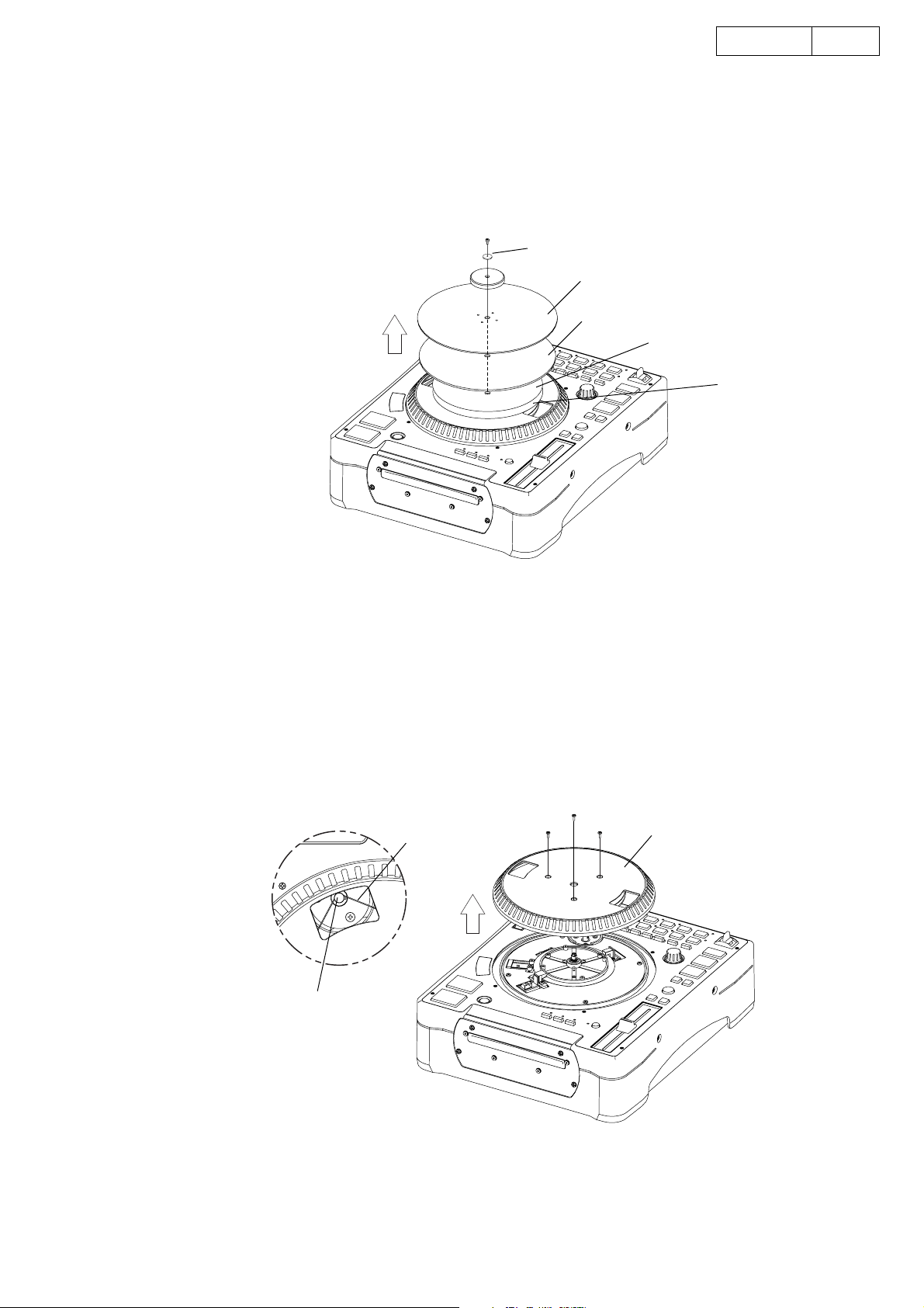
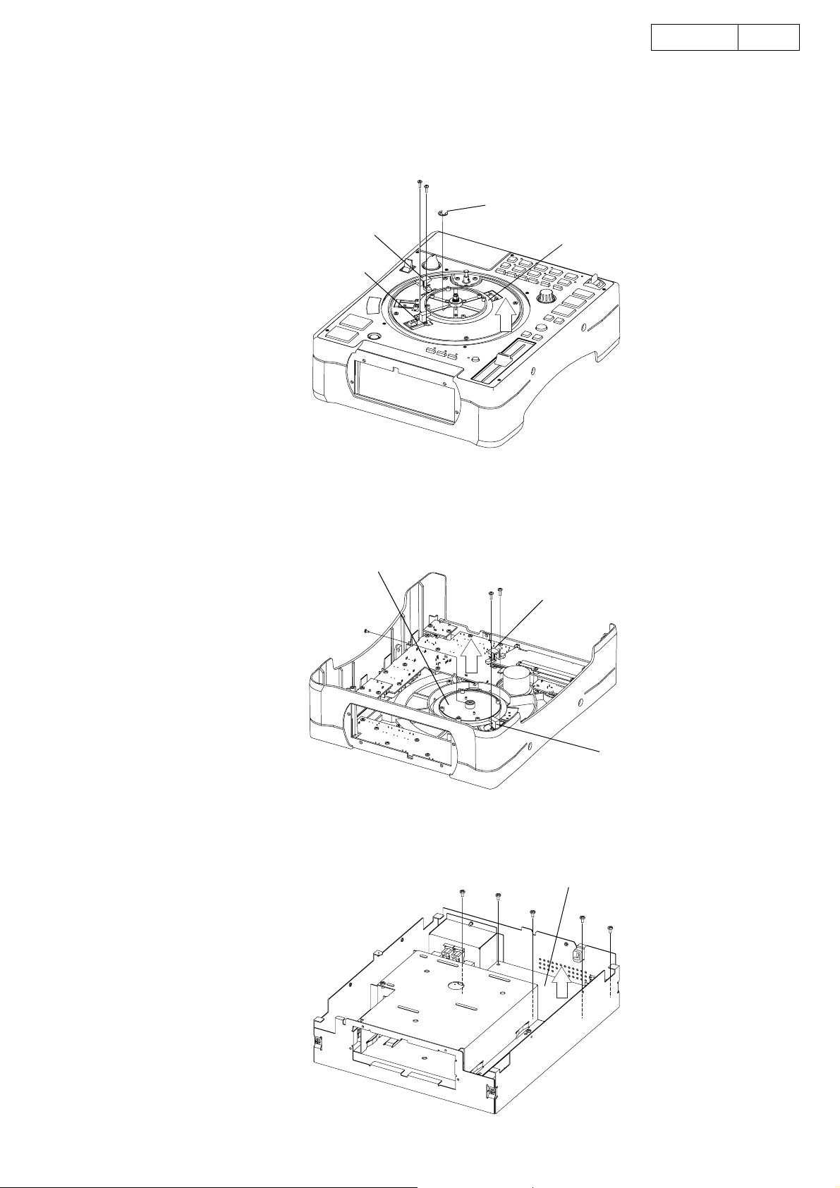
DISASSEMBLY
(Follow the procedure below in reverse order when reassembling.)
1. SLIP DISK, SLIP MAT
(1) Remove a screw and pull out Slip Disc and Slip Mat.
.
3DN-S3000
Washer
Slip Disc
Slip Mat
Slip Sheet
Anti-static Sheet
2. PLATTER
(1) Remove Belt from Motor Pully.
(2) Remove 3 screws and pull out Platter.
.
Motor Pully
Belt
Platter
3
Page 4
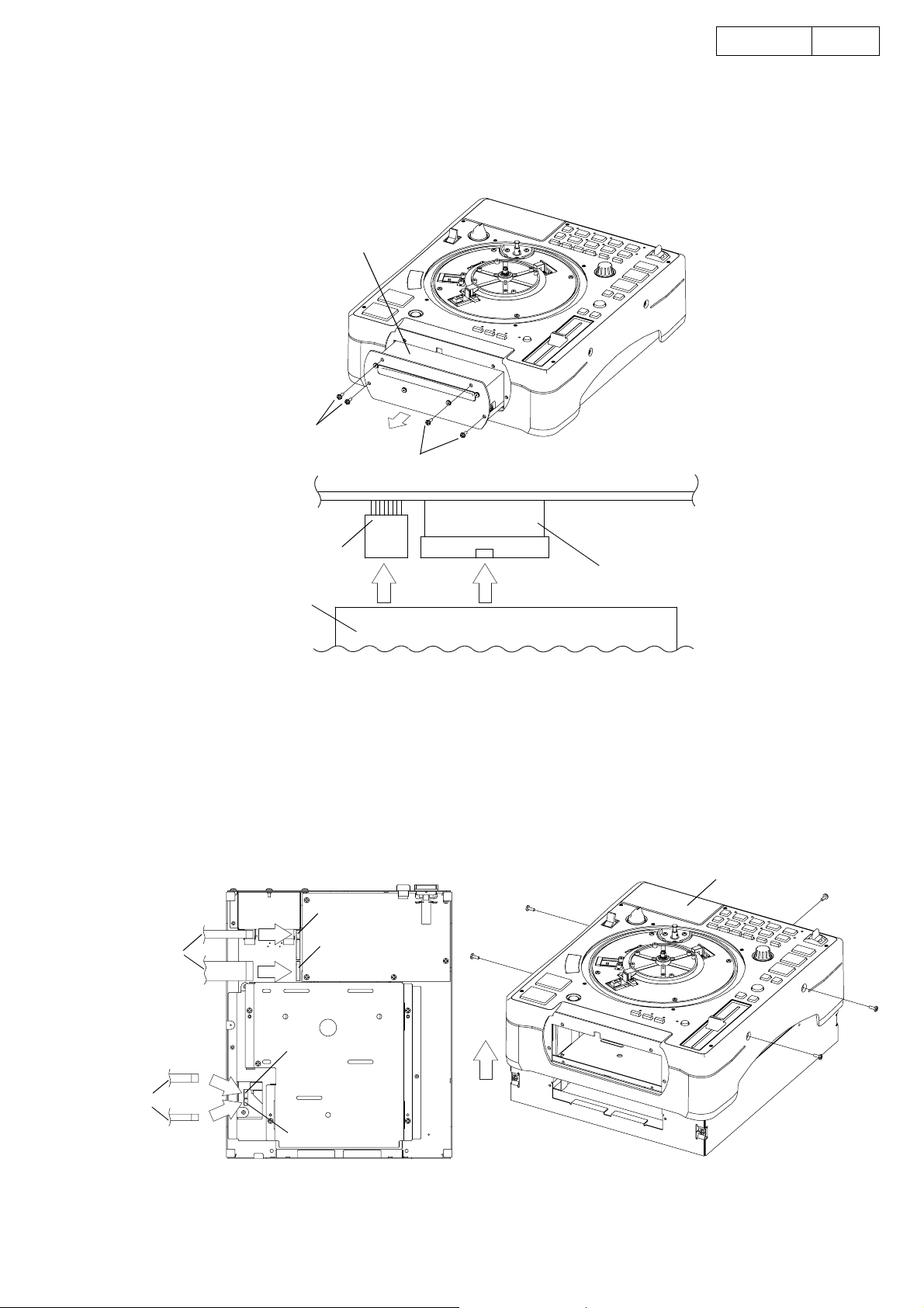
3. DRIVE UNIT
(1) Remove 4 screws and pull out Drive Unit.
(2) Disconnect Flat cable and Connector.
(3) Detach Drive Unit.
Drive Unit
71
4DN-S3000
71
Connector
Flat cable
Drive Unit
Note:
z Do not pull out aslant to prevent Flat cable damage.
z Do not fail to pull AC cord from wall outlet before disconnect the Flat cable and Connector.
If AC cord is remained plugged into wall outlet, power is kept supplied in the unit, which may cause danger.
4. COVER UNIT
(1) Remove 5 screws and pull out Cover Unit.
(2) Disconnect Connectors.
(3) Detach Cover unit.
CX042
Connector
CX101
Cover unit
CX041
Connector
CX031
Note:
z Do not fail to pull AC cord from wall outlet before disconnect Connectors.
If AC cord is remained plugged into wall outlet, power is kept supplied in the unit, which may cause danger.
4
Page 5
5. SENSOR AND SCALE UNITS OF PLATTER
(1) Remove 2 screws and pull out Sensor Cover and Sensor unit.
(2) Remove a E Ring.
(3) Pull out Scale unit.
5DN-S3000
E Ring
Sensor Cover
Sensor unit
6. SENSOR AND SCALE UNITS OF SLIP DISC
(1) Remove 2 screws and pull out Sensor Cover and Sensor unit.
(2) Remove a screw and pull out Scale unit.
Scale unit
Scale unit
Sensor Cover
7. POWER PWB
(1) Remove 5 screw and pull out Power PWB.
Sensor unit
Power PWB
5
Page 6
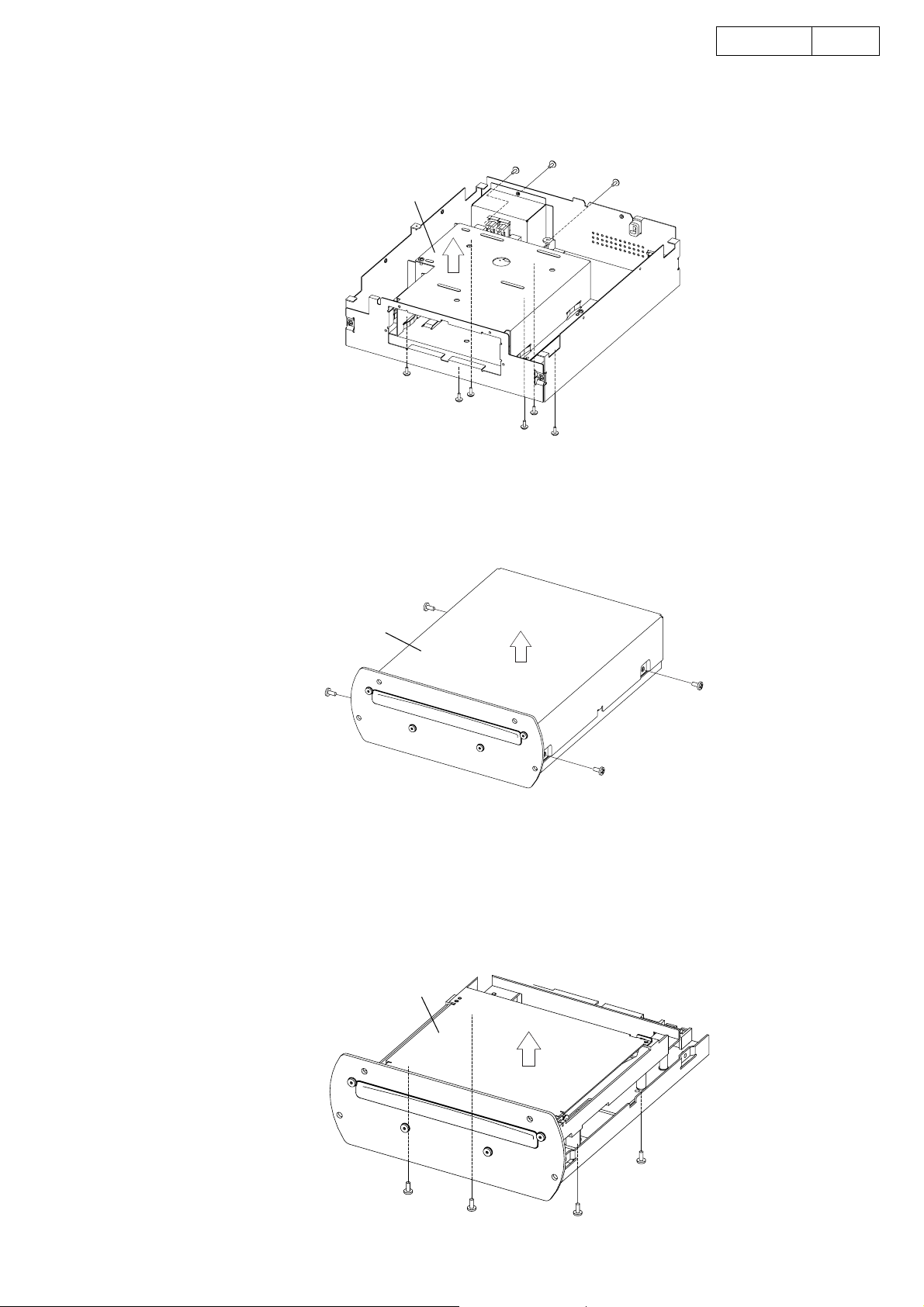
8. DSP PWB UNIT
(1) Remove 9 screws and pull out DSP PWB unit.
DSP PWB unit
9. DRIVE COVER
(1) Remove 4 screws and pull out Drive cover.
6DN-S3000
Drive cover
10. DRIVE
(1) Move Drive Rack in arrow direction through the Hole on the bottom chassis.
Loader frame comes out.
(2) Pull up Loader panel while pulling it towards front.
(3) Remove 4 screws and pull out Drive.
Drive
6
Page 7
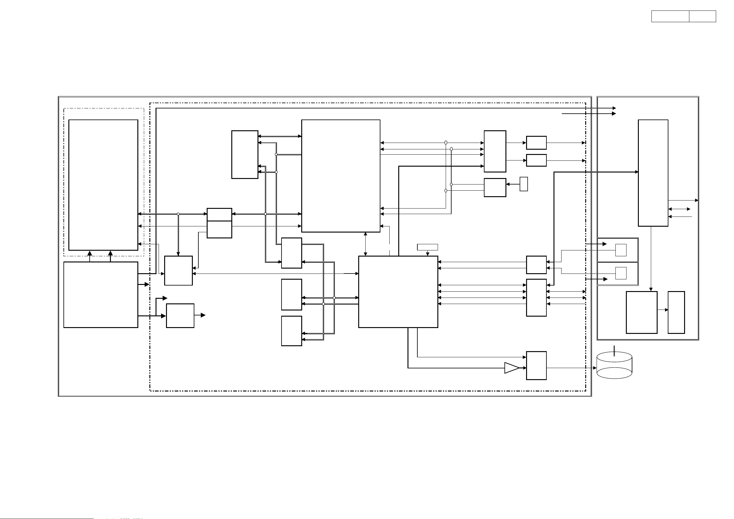
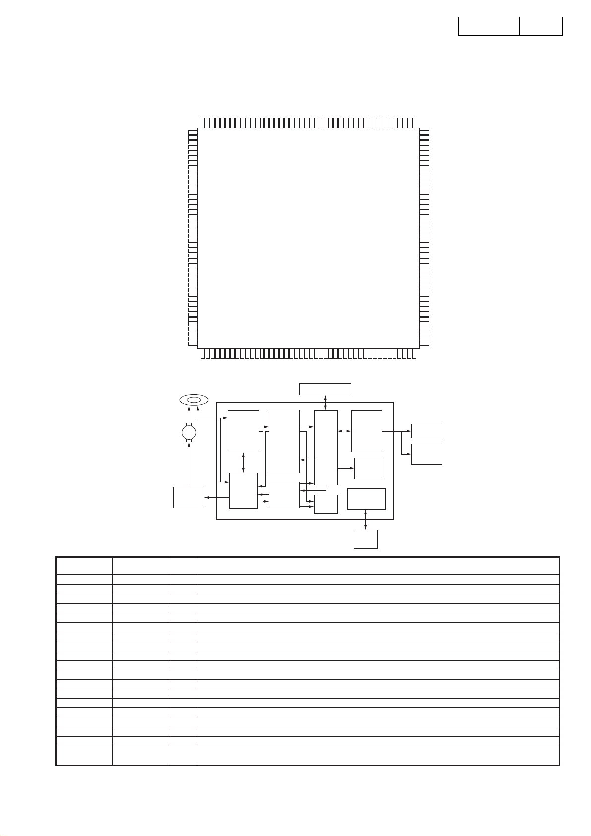
BLOCK DIAGRAM
DN-S3000
7DN-S3000
-HB,F1,F2
GND,+5
ROM
DRIVE
ATAPI
INTERFACE
9V 5.0V
SWITCHING
POWER SUPPLY
ATAPI
interface
-HB,F1,F2
±9.0V
5.0V
Interface
TMP86CM47U
5.0V
ATAP
CPU
Ragurater
128M
D16~31
SDRAM
RAM
32bit BUS
ADRESS
ADSP21065L
TXD0A
TXD0B
DSP
SHOCK PROOF
TXD1B CLOCK TMP86CM47U
BUS
select TXD1A
16Bit Bus TCK1
D0~D15
DMA
D0~15
CPU DSP 32.0M 32.0M 5v
BUS
interface
micon SERIAL 2
8M
FRASH
memory
3.3V
memo
4M
FRASH D/A
memory
RAM control
D0~D16
ADRESS
TFS0
TCK0
TFS1
FLAG
CONTROL
SYSTEM
CPU
MN102H730F
RAM10K
LRCK
BCLK
MAIN
D/A
DIT
AK4353
AMP
Trans
analog out
digital out
MAIN DOUT
256fs
DISC RV PULSE DISC
URN TABLE DIR TURN TABLE
SERIAL 1
UART
FW PULSE
UART
SERIAL 3
UART
DRIVER
PANEL
X'EFFECT IN
X'EFFECT OUT
3.3-5V FADER
adress
5v
DISC
SENSORSENSOR
TURN TABLE
ML9207
PANEL
µcom
ROM32k
RAM1k
LED out
Key scan
VR in
HB
FLTFLT Driver
CONTROL
motor
driver
Motor
7
Page 8
8DN-S3000
CONFIRMING THE SERVO
Required Measuring Implement
z Reference disc (TCD784 or CO-74176)
1. What is Service Program
Service program is a special program intended for confirming servo functions etc.
2. Contents of Service Program
Switch on the power while pushing the PITCH BEND + button and SCRATCH MODE button at the same time. After actuating
the servo program, select an aiming process number with the SELECT knob, A button, B button, SAMP button, or SAMP B
button. Press the SELECT knob to execute the selected process, the process number is then displayed on the track indicator
of the display. To exit from the service program, just switch off the power.
Process No.
(TRACK
Indication)
01
02
03
04
05
SELECT knob
06
07
Function
(Character-display)
com Version check
(Version No.)
OPEN/CLOSE
(Open Close)
Drive Diagnostic
(Drive_Diag)
Drive Data Read
(Data Read)
Error Code Check
(Error Data)
Total Running Time
(Total_Time)
Automatic
Servo Adjustment
call
Contents
Check Version with JOG dial.
1. System com version No.: “Sys_XXXX ”
2. DSP soft version No.: “Dsp_XXXX ”
3. ATAPI com version No.: “Atapi_XXXX ”
4. PANEL com version No.: “Panel_XXXX
5. ROM drive mecha. com version No.: “Drive_XXXX ”
Performs open/close each time when the SELECT knob is pushed.
ROM drive performs operation check when the SELECT knob is pushed, and
indicates the operational result. If the disc holder open, it starts the operation check
after closing. It indicates “Normal_End” if it ends normal. In case of error, ROM
drive error code is displayed in the character’s lower portion as “E
Starts continuous playback at its maximum reading speed from the beginning of
disc when the SELECT knob is pushed. It halts reading and stops if the knob is
pushed again.
Turn the PLATTER to display the logging error codes in the occurred order.
(“Error Data” is displayed.)
10 error logs are memorized at maximum.
Kinds of Error Code, displayed
Error Code Table (Appears only at Heat Run and Chucking Test function)
Pressing SELECT knob enters to data erase mode. (“Err Clear?” is displayed.)
If the SELECT knob is pushed again, the memorized error data are cleared.
Total time span of servo function that counted by the hour is displayed.
(“Total Time” is displayed.)
The display time is less than 65535 hours.
Note: No time is counted if powered down within 59 minutes.
Pressing SELECT knob enters to data erase mode. (“Time Clear?” is displayed.)
If the SELECT knob is pushed again, the memorized time data are cleared.
Starts automatic servo adjustment when the SELECT knob is pushed, and after
completing the adjustment, sort of the used disc is indicated. Data is selectable with
the PLATTER.
1. Disc check, CD/CD-RW
2. Focus gain data
3. Focus balance data
4. Focus offset data
5. Tracking gain data
6. Tracking balance data
7. Tracking offset data
8. PreAMP Tracking Sensor Gain
9. DSP Tracking Sensor Gain
10. PI offset
”
”.
****
サービスモード
サービスモードは、サーボ状態などを確認するための特別なプログラムです。
1. サービスプログラムの内容
PITCHBEND +ボタンと SCRATCHMODE ボタンを両方押しながら、電源を投入するとサービスモードになります。パラメータノブで各チェック項目
が、A ボタン ,B ボタン ,SAMP ボタン , または SAMPB ボタンで各テスト項目が選択できます。パラメータノブを押すか、PLAY/PAUSE ボタンを押すと各
項目のチェック、テストを開始し、その結果を表示します。
サービスモードをキャンセルするには、電源を切ってください。
*リファレンスディスク:TCD784、CO-74176
チェック項No.
( トラック番号 )
01 マイコンバージョンチェツク
02 CDEJECT パラメータノブを押すと CD の EJECT/LOAD が選択できます。
03 CD ドライブチェック
04 ドライブデータリード
05 エラーコードチェック
パラメータノブ
06 トータルランニングタイム
07 サーボ自動調整値
機能
キャラクター表示
VersionNo
(DriveDiag)
(DataRead)
(ErrorData)
(TotalTime)
読み出し
(ServoData)
内容
スクラッチディスクを回して、バージョンをチェックします。
1.システムマイコンバージョン No:"SysXXXX"
2.DSP ソフトバージョン No:"DspXXXX"
3.ATAPI マイコンバージョン No:"AtapiXXXX"
4.パネルマイコンバージョン No:"PanelXXXX"
5.CD ドライブマイコンバージョン No:"DriveXXXX"
パラメータノブを押すと CD ドライブの動作チェックを開始します。終了すると結果を表示し
ます。OK のときは NormalEnd が表示されます。
パラメータノブを押すと、データリードを開始し再生を開始します。再度、パラメータノブを押
すと、データリードを停止し、再生を停止します。
通常動作時、発生したエラーのエラーコードが表示されます。ディスクを回すと、最大 10 個
まで、記憶されたエラーデータが選択できます。( エラーコードはエラーコード表を参照下さい。)
・パラメータノブを押すと、エラーデータ消去モードになります。(ErrClear?が表示されます )
再度、パラメータノブを押すと、全てのエラーデータが消去されます。
スピンドルモータのトータル動作時間を表示します。1 時間単位で 65535 時間まで計測でき
ます。注意 )59 分以下で電源を切るとカウントされません。
・パラメータノブを押すと、トータル時間消去モードになります。(TimeClear?が表示されま
す ) 再度、パラメータノブを押すと、トータル時間が消去されます。
パラメータノブを押すとサーボ自動調整を開始します。調整が終了すると、調整データ表示
します。データはスクラッチディスクを回すことで選択できます。
1. ディスクチェック、CD/CD-RW
2. フォーカスゲインデータ
3. フォーカスバランスデータ
4. フォーカスオフセットデータ
5. トラッキングオフセットデータ
6. トラッキングバランスデータ
7. トラッキングオフセットデータ
8. プリアンプトラッキングセンサーゲイン
9.DSP トラッキングセンサーゲイン
10.PI オフセット
8
Page 9
3. TEST MODE
Process No.
(TRACK
Indication)
A button
B button
SAMP
button
SAMP B
button
-
-
-
-
Adjustment Item
Adjustment Value indication at
character portions.
1 Focus Gain 35 ~ 120
2 Focus Balance
3 Focus Offset
-20 ~ +20
-20 ~ +20
4 Tracking Gain 35 ~ 120
5 Tracking Balance
6 Tracking Offset
-20 ~ +20
-20 ~ +20
* Reference data.
Function
(Character-display)
Heat Run
(H/R1_Normal)
Chucking Test
(H/R2_Tray)
System check
(Sys._Check)
Starting with the PLAY/PAUSE button, it repeats open/close of the tray and
playback.
All tracks are played back if the track count is less than 20. Only the first and last
tracks are played back if the tracks are more than 21. When any errors, it stops
and indicates error code (see Error Code Table).
Starting with the PLAY/PAUSE button, it repeats open/close of the tray, servo on,
and TOC read.
The display shows the number of the tray operation. When any errors, it stops and
indicates error code (see Error Code Table).
It starts system check when the PLAY/PAUSE button is pushed, and indicates the
status by performing plain operational check in the system .
1. Communication judge between the system com and DSP
2. DSP SDRAM write/read operation check
3. Communication judge between the system com and ATAPI com
4. Communication judge between the ATAPI com and ROM drive
5. ROM drive operation check
After finishing the check, it indicates the result on the character display lower
portion.
When the 1. ~ 5. items are OK, their item numbers are indicated.
But if there is a NG item, its item number is not indicated.
Judges whether PLATTER can rotate at the specified rotating speed.
The message "Platter_OK" is displayed on the character display if the rotating
speed meets the specification. Otherwise, "Platter_NG" is displayed.
Contents
サーボ自動調整読み出し値
サーボ調整項目 調整 OK 範囲
1 フォーカスゲイン 35 〜 120
2 フォーカスバランス -20 〜 +20
3 フォーカスオフセット -20 〜 +20
4 トラッキングゲイン 35 〜 120
5 トラッキングバランス -20 〜 +20
6 トラッキングオフセット -20 〜 +20
2. テストモード
機能キャラクター表示 内容
A ボタン ヒートランテスト
H/R1Normal
A1 ボタンを押し、PLAY/PAUSE ボタンを押すとテストを開始します。
ディスクの出し入れと、再生を繰り返します。
20 トラック以下のディスクのときは、全てのトラックを再生します。
21 トラック以上のディスクのときは、ディスク先頭トラックと最終トラックのみ再生します。エラーが発生すると、エラーコード
を表示して停止します。
B ボタン チャッキングテスト
H/R2Tray
A2 ボタンを押し、PLAY/PAUSE ボタンを押すとテストを開始します。
ディスクの出し入れと、サーボ投入、TOC の読み込みを繰り返します。
エラーが発生すると、エラーコードを表示して停止します。
SAMP ボタン システムチェック
Sys.Check
A3 ボタンを押し、PLAY/PAUSE ボタンを押すとシステムチェックを開始し、チェック終了後、その結果を表示します。
1. システムマイコンと DSP の通信チェツクを行います。
2.DSP が SDRAM のリード / ライトチェツクを行います。
3. システムマイコンと ATAPI マイコンの通信チェツクを行います。
4.ATAPI マイコンと CD ドライブの通信チェツクを行います。
5.CD ドライブの動作チェックを行います。
全てのチェックが終了すると、キャラクター表示に結果を表示します。1 〜 5 項目のチェックが OK の時は、OK に
なった項目の番号が表示されます。NG の項目が合った場合、NG になった項目の番号が表示されま
せん。
SAMPB ボタン プラターチェック
PlateCheck
A4 ボタンを押し、PLAY/PAUSE ボタンを押すとプラターの回転チェックを開始し、チェック終了後、その結果を表示
します。プラターの回転をチェツクし OK のとき "PlatterOK" を表示します。NG のとき "PlatterNG" を表示
します。
3. エラーコードテーブル ( ヒートランテスト、及び、チャッキングテストのとき表示されます )
9DN-S3000
4. Error Code Table (Appears only at Heat Run and Chucking Test function)
Error Code Contents
Automatic Adjustment Error
E1 00
E1 01
E1 03
E1 04
E1 05
E1 06
E2 02 Servo down during automatic adjustment
E3 00 Unable to read TOC
E4 00
E4 01
E5 00 Slide error
Unable to detect disc
Unable to adjust tracking offset
Unable to adjust focus fine gain
Unable to actuate focus
Unable to actuate tracking
Unable to adjust tracking fine gain
Unable to close the disc holder in the regular time
Unable to open the disc holder in the regular time
エラーコード
内容
サーボ自動調整エラー
E100
E101
E103
E104
E105
E106
ディスクが検出できない。
トラッキングオフセットが調整できない。
フォーカスゲインが調整できない。
フォーカスサーボが入らない。
トラッキングサーボが入らない。
トラッキングゲインが調整できない。
E202 サーボ自動調整中サーボが外れた。
E300 TOC が規定時間内に読めない。
E400
E401
ディスクが規定時間内にローディングできない。
ディスクが規定時間内にイジェクトできない。
E500 スライドエラー
9
Page 10
Detailed error can be displayed by PLATTER when error occurs.
10DN-S3000
Error Indication
TR MIN SEC FRAM CHARACTER
Displays the track
No. in which error
occurred.
Displays the time at which error occurred. “H
Operation count Error code
* * * *E * * *
”
5. System µcom and DSP Version Upgrade
System µcom and DSP can be upgraded in the following manner.
Version Upgrade Method
(1) Record the version upgrade software on a CD-R or CD-RW disc, only as one file with the format ISO9660 Mode-1.
The file name of the supplied version upgrade software should be used as is and this disc needs to finalize.
(2) After loading the disc made in above step 1, turn off the power. Then, turn on the power while pressing the NEXT TRACK
button and FAST SEARCH FWD ( ) button. The version upgrade starts with reading data of the disc.
(3) When you start version upgrade operation, messages "Version_Up" and "System&DSP" are displayed on the character dis-
play.
Recovery positions are turned on one by one from the left end according as the upgrade operation proceeds. When this operation is completed, all recovery positions are turned on.
In case of some error or the power is turned off during the version upgrade, it may be impossible to operate at all thereafter.
Changing of IC502 on GU-3546 is necessary in this case, and software writing to IC502 should be done beforehand.
(4) When the upgrade is completed, the disk is ejected and operation returns to the normal mode.
(5) File name of the upgrade software indicates version numbers.
File name T3.
System com
* * * * * *
version
. BIN
DSP version
6. ROM Drive (FG-5000) µcom Version Upgrade
Drive (FG-5000) µcom can be upgraded in the following manner.
Version Upgrade Method
(1) Record the version upgrade software on a CD-R or CD-RW disc, only as one file with the format ISO9660 Mode-1.
The file name of the supplied version upgrade software should be used as is and this disc needs to finalize.
(2) After turning on the power, load the disc made in above step 1 into the mecha. you want to upgrade the version.
(3) "Drive" and "Version UP?" are indicated in the character display. Press the CD EJECT button and remove the disc when not
upgrade the version.
(4) Press the PLAY/PAUSE to start the version upgrade. "Now Loading" is indicated.
(5) When the version upgrade is finished, "Complete" is indicated and the disc EJECT.
(6) Turn off the power once and turn on again after take out the disc.
The version upgrade ends in 20~30 seconds normally. If the power turned off underway or the version upgrade ends
abnormally, the drive may become malfunction. In such a case, version upgrade with PC will be needed.
(7) File name of the upgrade software indicates version number.
File name FG5K
* * * *
. BIN
エラー表示
トラック 分 秒 フレーム キャラクター
エラーが発生した
トラック番号
エラーが発生した時間 (A タイム ) H ****動作回数
E ****エラーコード
4. マイコンアップデート
DN-S5000 は、ディスクから、システムマイコン、DSP、CD ドライブマイコンのアップデートを行うことができます。
(1) アップデートディスクの作成
システムマイコン、DSP、ドライブマイコンのアップデート用ディスクディスクを下記に従い作成下する。
① アップデート用のソフトを、CD-R、又は CD-RW ディスクに ISO9660,MODE1 のフォーマットで記録し、ファイナライズする。
・ 配布されたアップデートファイルを、CD ライティングソフトで DISCATONCE で書き込みしファイナライズする。
・ システムマイコン (DSP を含む ) とドライブマイコンの2個のアップデートソフトを 1 枚のディスクに記録出来ます。その他のソフトやデータを同一ディスク内
に記録しないこと。
・ ファイル名は、配布されたときのファイル名をそのまま使用すること。
(2) システムマイコン、DSP のアップデート
① (1) で作成したディスクをローディングし、電源を切り、NEXTTRACK と FASTSEARCHFWD( ) ボタンを押しながら電源を入れると、
ディスクのデータを読みとりアップデートを開始します。
② アップデートを開始すると、"VersionUp"、"System & DSP" が表示されます。
アップデートの進行に合わせ、再生位置表示が左から右へ順に点灯し、終了すると、全ての表示が点灯します。
注意 ) 大変希ではありますが、アップデート中に、アップデート未終了の異常状態が発生することがあります。アップデートを開始し3分
を経過しても終了しない場合も、異常が発生したと考えられますので、電源を切って、再度、(2) ①から同一の操作を行って
下さい。
発生した異常状況により、以後の全ての動作が出来なくなることがあります。その場合、GU-3546IC502 の交換が必要にな
ります。IC502 は、予め、ソフトウエアを書き込みする必要があります。(IC502 を発注の際は、最新のシステムマイコンバージョン No(GENNo)
で発注願います。)
③ アップデートが終了すると、ディスクがイジエクトされます。
(3) ドライブマイコンのアップデート
①システムマイコンのバージョンアップに引き続き、ドライブマイコンのバージョンアップを実施する場合は、再度、ディスクをローディングします。
・ドライブマイコンのみバージョンアップする場合、電源投入後、(1) で作製したディスクを最初にローディングします。
②ドライブ用のアップデートソフトが認識されると、表示にDriveVersionUP?が表示されます。
③ PLAY/PAUSE ボタンを押すと、アップデートを開始し、NowLoading が表示されます。
④アップデートが終了すると、Complete が表示され、ディスクがイジェクトされます。
⑤電源を切って終了です。
注意 ) 大変希ではありますが、アップデート中に異常が発生することがあります。
アップデートを開始し 3 分を経過しても終了しない場合も、異常が発生したと考えられますので、電源を切って、再投入して下さ
い。
但し、アップデート開始から終了までの間に機器の電源を切った場合、又は異常が発生した場合、ドライブが動作しなくなることが
あります。その場合、パソコンからのアップデートが必要になります。そのような場合は、QA に連絡願います。
Version number
10
Page 11
SEMICONDUCTORS /半導体一覧表
Only major semiconductors are shown, general semiconductors etc. are omitted to list.
主な半導体を記載しています。汎用の半導体は記載を省略しています。
1. IC’s
Note : Abbreviation ahead of IC No. indicates the name of P.W.B., etc.
注 ): ICNo. の前の記号は、基板の名称を表します。
DS : DSP P.W.B.
PA : PANEL P.W.B.
CD : CD-ROM P.W.B.
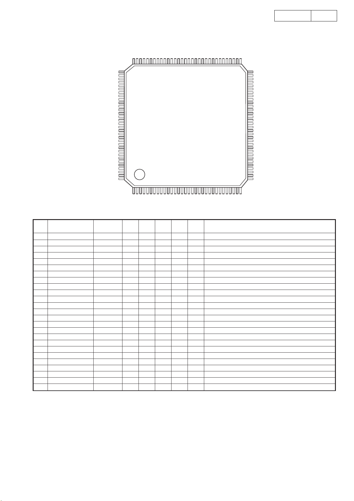
ADSP-21065L (DS: IC401)
208 157
11DN-S3000
156
105
52
1
TOP VIEW
53
104
ADSP-21065L Terminal Function
Pin
No.
1VDD VDD VDD —————Power (+3.3V)
2 RFS0 YLRCK YLRCK I — IPu — H
3GND GND GND —————GND
4 RCLK0 YBCK YBCK I — — — — Receive frame sync (BCK) signal (Serial port IN 0)
5 DR0A ADDATA ADDATA I — IPu — H Data receive A (serial port IN 0)
6 DR0B I — IPu — H Data receive B (serial port IN 0)
7 TFS0 YLRCK YLRCK I — IPu — H
8 TCLK0 YBCK YBCK I — — — — Send frame sync (BCK) signal (Serial port OUT 0)
9VDD VDD VDD —————Power (+3.3V)
10GND GND GND —————GND
11 DT0A MOUT1 MOUT2 O — IPu — H Data send A (Serial port OUT 0)
12 DTOB DOUT1 DOUT2 O — IPu — H Data send B (Serial port OUT 0)
13 RFS1 LRCK1 LRCK2 I — IPu — H
14GND GND GND —————GND
15 RCLK1 BCK1 BCK2 I — — L — Receive frame sync (BCK) signal (Serial port IN 1)
16 DR1A SAMP2 SAMP1 I — IPu — H Data receive A (serial por t IN 1)
17 DR1B I — IPu — H Data receive B (serial port IN 1)
18 TFS1 LRCK2 LRCK1 I/O — IPu — H
19 TCLK1 BCK2 BCK1 I/O ————Send frame sync (BCK) signal (Serial port OUT 1)
20
21VDD VDD VDD —————Power (+3.3V)
22 DT1A SOUT1 SOUT2 O — IPu — H Data send A (Serial port OUT 1)
23 DT1B SAMP1 SAMP2 O — IPu — H Data send B (Serial port OUT 1)
24 PWM_EVENT1 I/O — Pd — L PWM1 output
25GND GND GND —————GND
26 PWM_EVENT0 I/O — Pd — L PWM0 output
27 BR1_ I — Pu — H Multi-processing bus request 1
28 BR2_ I — Pu — H Multi-processing bus request 1
29VDD VDD VDD —————Power (+3.3V)
30 CLKIN I — — — — Clock input
31 XTAL_ O — — — — X’tal oscillator pin
32VDD VDD VDD —————Power (+3.3V)
Port Name
VDD VDD VDD —————Power (+3.3V)
Symbol
(IC301)
Symbol
(IC401)
I/O DET Ext Ini
Res
Receive frame sync (LRCK) signal (Serial port IN 0)
Send frame sync (LRCK) signal (Serial port OUT 0)
Receive frame sync (LRCK) signal (Serial port IN 1)
Send frame sync (LRCK) signal (Serial port OUT 1)
Function
11
Page 12
12DN-S3000
Pin
No.
33GND GND GND —————GND
34 SDCLK1 O — Pd — L SDRAM clock enable 1
35GND GND GND —————GND
36VDD VDD VDD —————Power (+3.3V)
37 SDCLK0 I/O ————SDRAM clock enable 0
38 DMAR1_ I — Pu H H DMA request 1
39 DMAR2_ I — Pu H H DMA request 2
40 HBR_ I — Pu — H Host bus request (BOOT)
41GND GND GND —————GND
42 RAS_ I/O — Pu H H SDRAM row access strobe
43 CAS_ I/O — Pu H H SDRAM column access strobe
44 SDWE_ I/O — Pu H H SDRAM write enable
45VDD VDD VDD —————Power (+3.3V)
46 DQM O — — — — SDRAM data mask
47 SDCKE I/O — — H — SDRAM clock enable
48 SDA10 O — Pd L L SDRAM A10
49GND GND GND —————GND
50 DMAG1_ O — — H — DMA ground 1
51 DMAG2_ O — — H — DMA ground 2
52 HBG_ O — — H — Host bus ground (BOOT)
53 BMSTR O — — H — Bus master output (H out)
54VDD VDD VDD —————Power (+3.3V)
55 CS_ I — — L L Chip select (BOOT)
56 SBTS_ I — Pu H H Extend bus three state
57GND GND GND —————GND
58WR_ I/O————Memory write strobe
59RD_ I/O————Memory read strobe
60GND GND GND —————GND
61VDD VDD VDD —————Power (+3.3V)
62GND GND GND —————GND
63 REDY O — — — — Host bus ACK
64SW_ I/O————Sync type write select
65CPA_ I/O————Core priority access
66VDD VDD VDD —————Power (+3.3V)
67VDD VDD VDD —————Power (+3.3V)
68GND GND GND —————GND
69ACK I/O————Memory ACK
70 MS0_ I/O — Pu H H Memory select 0
71 MS1_ I/O ————Memory select 1
72GND GND GND —————GND
73GND GND GND —————GND
74 MS2_ I/O ————Memory select 2
75 MS3_ I/O ————Memory select 3
76 FLAG11
77VDD VDD VDD —————Power (+3.3V)
78 FLAG10
79 FLAG9 JOGB1 JOGB2 I — — — —
80 FLAG8 JOGA1 JOGA2 I — — — —
81 GND GND
82DATA0 I/O————Ext. bus data 0
83DATA1 I/O————Ext. bus data 1
84DATA2 I/O————Ext. bus data 2
85VDD VDD VDD —————Power (+3.3V)
86DATA3 I/O————Ext. bus data 3
87DATA4 I/O————Ext. bus data 4
88DATA5 I/O————Ext. bus data 5
89GND GND GND —————GND
90DATA6 I/O————Ext. bus data 6
91DATA7 I/O————Ext. bus data 7
92DATA8 I/O————Ext. bus data 8
93VDD VDD VDD —————Power (+3.3V)
94GND GND GND —————GND
Port Name
Symbol
(IC301)
DMABSY1
SAMPCOP
Symbol
(IC401)
DMABSY2
SAMPCOPY
GND —————GND
I/O DET Ext Ini
O — Pu — H General flag 11 (In DMA flag L: DMA)
I/O — Pu — H General flag 10 (In SAMPLER copy flag)
Res
General flag 9 (JOG turning direction detect signal B)
General flag 8 (JOG turning direction detect signal A)
Function
12
Page 13
13DN-S3000
Pin
No.
95VDD VDD VDD —————Power (+3.3V)
96DATA9 I/O————Ext. bus data 9
97DATA10 I/O————Ext. bus data 10
98DATA11 I/O————Ext. bus data 11
99GND GND GND —————GND
100DATA12 I/O————Ext. bus data 12
101DATA13 I/O————Ext. bus data 13
102NC —————NC
103NC —————NC
104DATA14 I/O————Ext. bus data 14
105VDD VDD VDD —————Power (+3.3V)
106GND GND GND —————GND
107DATA15 I/O————Ext. bus data 15
108DATA16 I/O————Ext. bus data 16
109DATA17 I/O————Ext. bus data 17
110VDD VDD VDD —————Power (+3.3V)
111DATA18 I/O————Ext. bus data 18
112DATA19 I/O————Ext. bus data 19
113DATA20 I/O————Ext. bus data 20
114GND GND GND —————GND
115NC —————NC
116DATA21 I/O————Ext. bus data 21
117DATA22 I/O————Ext. bus data 22
118DATA23 I/O————Ext. bus data 23
119GND GND GND —————GND
120VDD VDD VDD —————Power (+3.3V)
121DATA24 I/O————Ext. bus data 24
122DATA25 I/O————Ext. bus data 25
123DATA26 I/O————Ext. bus data 26
124VDD VDD VDD —————Power (+3.3V)
125GND GND GND —————GND
126DATA27 I/O————Ext. bus data 27
127DATA28 I/O————Ext. bus data 28
128DATA29 I/O————Ext. bus data 29
129GND GND GND —————GND
130VDD VDD VDD —————Power (+3.3V)
131VDD VDD VDD —————Power (+3.3V)
132DATA30 I/O————Ext. bus data 30
133DATA31 I/O————Ext. bus data 31
134 FLAG7 DFLG12 DFLG22 I/O — Pu — H General flag 7 (RESERVE)
135GND GND GND —————GND
136 FLAG6 DFLG11 DFLG21 I/O — Pu — H General flag 6 (RESERVE)
137 FLAG5 DTIMB1 DTIMB2 O — — — —
138 FLAG4 DTIMA1 DTIMA2 O — — — —
139GND GND GND —————GND
140VDD VDD VDD —————Power (+3.3V)
141VDD VDD VDD —————Power (+3.3V)
142NC —————NC
143 ID1 I — — L L Multi-processing ID1 (Single processor : 0)
144 ID0 I — — L L Multi-processing ID2 (Single processor : 0)
145 EMU_ EMU1_ EMU2_ O — — — — Emulation status
146
147 TRST_ TRST1_ TRST2_ I — IPu — H Test reset (JTAG)
148 TDI TDI1 TDI2 I — Pd — L Test data input (JTAG)
149 TMS TMS1 TMS2 I — IPu — H Test mode select (JTAG)
150GND GND GND —————GND
151 TCK TCK1 TCK2 I — Pu — H Test clock (JTAG)
152 BSEL I — — H H EPROM boot select (Boot by EPROM: 1)
153 BMS_ BMS1_ BMS2_ I — — H H Boot memory select (Host processor boot: 1)
154GND GND GND —————GND
155GND GND GND —————GND
156VDD VDD VDD —————Power (+3.3V)
Port Name
TD0 TD01 TD02 O — — — — Test data output (JTAG)
Symbol
(IC301)
Symbol
(IC401)
I/O DET Ext Ini
Res
General flag 5 (Pulse output for generating monitor play time)
General flag 4 (Pulse output for generating main play time)
Function
13
Page 14
14DN-S3000
Pin
No.
157 RESET_ DRES_ DRES_ I — — H L DSP reset signal
158VDD VDD VDD —————Power (+3.3V)
159GND GND GND —————GND
160 ADDR23 I/O ————Ext. bus address 23
161 ADDR22 I/O ————Ext. bus address 22
162 ADDR21 I/O ————Ext. bus address 21
163VDD VDD VDD —————Power (+3.3V)
164 ADDR20 I/O ————Ext. bus address 20
165 ADDR19 I/O ————Ext. bus address 19
166 ADDR18 I/O ————Ext. bus address 18
167GND GND GND —————GND
168GND GND GND —————GND
169 ADDR17 I/O ————Ext. bus address 17
170 ADDR16 I/O ————Ext. bus address 16
171 ADDR15 I/O ————Ext. bus address 15
172VDD VDD VDD —————Power (+3.3V)
173 ADDR14 I/O ————Ext. bus address 14
174 ADDR13 I/O ————Ext. bus address 13
175 ADDR12 I/O ————Ext. bus address 12
176VDD VDD VDD —————Power (+3.3V)
177GND GND GND —————GND
178 ADDR11 I/O ————Ext. bus address 11
179 ADDR10 I/O ————Ext. bus address 10 (SDRAM: Connects SDA10)
180 ADDR9 I/O ————Ext. bus address 9
181GND GND GND —————GND
182VDD VDD VDD —————Power (+3.3V)
183 ADDR8 I/O ————Ext. bus address 8
184 ADDR7 I/O ————Ext. bus address 7
185 ADDR6 I/O ————Ext. bus address 6
186GND GND GND —————GND
187GND GND GND —————GND
188 ADDR5 I/O ————Ext. bus address 5
189 ADDR4 I/O ————Ext. bus address 4
190 ADDR3 I/O ————Ext. bus address 3
191VDD VDD VDD —————Power (+3.3V)
192VDD VDD VDD —————Power (+3.3V)
193 ADDR2 I/O ————Ext. bus address 2
194 ADDR1 I/O ————Ext. bus address 1
195 ADDR0 I/O ————Ext. bus address 0
196GND GND GND —————GND
197 FLAG0 DR_/W1 DR_/W2 I/O ————General flag 0 (Command read write select)
198 FLAG1 DACK1_ DACK2_ I/O ————General flag 1
199 FLAG2 DBSY1 DBSY2 I/O ————General flag 2
200VDD VDD VDD —————Power (+3.3V)
201 FLAG3 DFLG10 DFLG20 I/O — Pu — H General flag 3 (RESERVE)
202NC ——————
203NC ——————
204GND GND GND —————GND
205 IRQ0_ DREQ1 DREQ2 I — Pu — H Interrupt request input 0 (SYS mcom interface)
206 IRQ1_ DREQ1_ DREQ2_ I — Pu — L Interrupt request input 1 (SYS mcom interface)
207 IRQ2_ JOGINT1 JOGINT2 I — — — —
208
Port Name
NC —————NC
Symbol
(IC301)
Symbol
(IC401)
I/O DET Ext Ini
Res
Interrupt request input 2 (JOG turning speed detect signal)
Function
14
Page 15
M5705Q (CD: IC501)
15DN-S3000
AVSS-DS
XSRFIN
XSIPIN
AVDD5-DS
XSDSSLV
XSRSLINT
XSAWRC
XSRFGC
XSEFGC
XSFOCUS
XSTRACK
XSSLEG
AVDD5-DA
XSMOTOR
AVSS-DA
XSRFRPLP
XSTELP
XSVREF2
XSRFRP
XSTEXI
AVSS-AD
XSTEI
XSFEI
XSAEI
AVDD5-AD
XSSBAD
XSDFCT
XSCSJ
XSCLK
XSDATA
XSLDC
XSFGIN
XSSPDON
XSFLAG(3)
XSFLAG(2)
XSFLAG(1)
XSFLAG(0)
XMP1_7
XMP1_6
XMP1_4
XSPDOFTR2
XSVR_PLL
174
173
XMP1_2
XGPIO(2)
XSFTROPI
XSFDO
172
171
XMP1_1
XMRSTJ
AVSS_PL
XSPLLFTR2
170
169
XGPO(1)
XGPO(0)
VDD5_PL
A
XSFDIREF
168
167
XCRSTJ
XMPSENJ
XSPDIREF
GND
166
165
VDD
XMALE
XTSLRF
XTPLCK
164
163
VDD
XMP1_0
VDD
162
XOSC1
XRA(3)
161
XOSC2
XRA(2)
160
GND
XRA(1)
159
XMD(0)
XRA(0)
158
XMD(1)
XRA(4)
157
XMD(2)
XRA(5)
156
XMD(3)
XRA(6)
155
XMD(4)
GND
154
XMD(5)
XRA(7)
153
XMD(6)
XRA(10)
XRA(11)
152
151
XMCSJ
XMD(7)
VDD
150
XMRDJ
XRA(8)
149
XMWRJ
XRA(9)
XROEJ
148
147
XMA(11)
XMINT1J
VDD
146
XMA(10)
XSAWRCVCO
XSVREFO
176
175
1
2
3
4
5
6
VDD
7
8
9
10
11
12
13
14
15
16
17
18
19
20
21
22
23
24
25
26
27
GND
28
29
30
31
32
33
34
35
36
37
38
39
40
41
GND
42
NC
43
44
45464748495051525354555657585960616263646566676869707172737475767778798081828384858687
XMP1_3
XMFSCSJ
4M DRAM
M5705
XRCASJ
XRRASJ
145
144
VDD
XMA(9)
XRSDCLK
XRWEJ
143
142
XMA(8)
XMA(7)
XRD(7)
141
XMA(6)
XRD(8)
140
XMA(5)
XRD(6)
139
XMA(4)
GND
138
XMA(3)
XRD(9)
137
XMA(2)
XRD(5)
136
XMA(1)
XRD(10)
XRD(4)
135
134
XMA(0)
XMA(12)
XRD(11)
133
132
131
130
129
128
127
126
125
124
123
122
121
120
119
118
117
116
115
114
113
112
111
110
109
108
107
106
105
104
103
102
101
100
88
GND
99
98
97
96
95
94
93
92
91
90
89
XRD(3)
XRD(12)
GND
XRD(2)
XRD(13)
XRD(1)
XRD(14)
XRD(0)
XRD(15)
XHD(7)
XHD(8)
XHD(6)
XHD(9)
XHD(5)
XHD(10)
XHD(4)
XHD(11)
VDD
XHD(3)
XHD(12)
XHD(2)
XHD(13)
GND
XHD(1)
XHD(14)
XHD(0)
XHD(15)
XHDRQ
XHIOWJ
XHIORJ
XHIORDY
XHDACKJ
XHINT
XHCS16J
XHA(1)
XHPDIAGJ
XHA(0)
XHA(2)
XHCS1J
XHCS3J
XHDASPJ
XMA(15)
XMA(14)
XMA(13)
ATAP I
M
Motor
Driver
Data
Separator
Digital
Servo
DVD-DSP
CD-DSP
RAM
Arbiter
Target
Search
&
MPEG
I/F
C3 ECC
EDC
MCU
ROM
M5705 Terminal Function
Pin Name
Type
2 XSRFIN I/A Analog RF signal input after passing through the equalizer
3 XSIPIN I/A Inverting input pin of data slicer
5 XSDSSLV O/A Slice level output pin
6 XSRSLINT I/A Reference current setting pin for analog data slicer
8 XSAWRC O/A Output for enlarge VCO range. Analog output from DAC buffer
9 XSRFGC O/A RF gain control output
10 XSEFGC O/A E,F gain control output
11
XSFOCUS O/A Output voltage level for focusing buffer IC
12 XSTRACK O/A Output voltage level for tracking buffer IC
13 XSSLEG O/A Output voltage level for sledge buffer IC
15 XSMOTOR O/A Output voltage level for spindle motor buffer IC
17 XSRFRPLP I/A High bandwidth low pass filter input for RFRP
18 XSTELP I/A High bandwidth low pass filter input for TE
19 XSVREF2 I/A 2.1V reference voltage input
20 XSRFRP I/A RF ripple/envelope signal input
21 XSTEXI I/A Tracking zero crossing input signal
23 XSTEI I/A Tracking error input signal
24 XSFEI I/A Focus error input signal
25
XSCEI I/A
1. Center error input signal
2. Photo Interrupt input
DescriptionPin No.
PC
MPEG
DEC.
15
Page 16
16DN-S3000
Pin Name
27 XSSBAD I/A Sub-beam addition signal input
166 XSPDIREF I/A
167 XSFDIREF I/A
169 XSPLLFTR2 I/A Data PLL loop filter pin#2
171 XSFDO O/A Output node of frequency detector charge pump circuit
172 XSFTROPI I/A Input node of loop filter OP circuit
173 XSVR_PLL I/A PLL reference voltage input
174 XSPDOFTR2 I/A Phase detector filter pin#1
175 XSVREFO O/A Reference voltage output
176 XSAWRCVCO I/A Auto Wide Range Control of VCO input pin. For enlarge VCO range in CAV mode
29 XSDFCT I Detect detection signal input
30 XSCSJ O Chip select signal for accessing control registers
31 XSCLK O Clock output for accessing control registers
32 XSDATA I/O Registers data input/output pin
33 XSLDC O Laser diode on/off control output for both CD/DVD
34 XSFGIN I Motor Hall sensor input
35 XSSPDON O Spindle motor on output
36, 37, 38, 39 XSFLAG[3:0] O These pins are used to monitor some status of servo control block
48, 51, 52 XGPIO[2:0] I/O
40 XMP1_7 I/O Internal microcontroller programmable I/O port 1.7.
41 XMP1_6 I/O Internal microcontroller programmable I/O port 1.6.
43 XMP1_5 I/O This pin is now changed to be NC.
44 XMP1_4 I/O Internal microcontroller programmable I/O port 1.4.
45 XMP1_3 I/O Internal microcontroller programmable I/O port 1.3.
47 XMP1_2 I/O Internal microcontroller programmable I/O port 1.2.
49 XMP1_1 I/O Internal microcontroller programmable I/O port 1.1.
57 XMP1_0 I/O
46 XMFSCSJ I/O Output chip select connected to external flash ROM chip enable pin
54 XMPSENJ I/O Output program store enable connected to external ROM PSENJ pin.
56 XMALE I/O This signal is used as address latch signal in address/data mux mode
70 XMCSJ I/O
71 XMRDJ I/O
72 XMWRJ I/O This signal is used as the Wire Strobe signal
73 XMINT1J I/O
74, 75, 77, 78,
79, 80, 81, 82,
83, 84, 85, 86,
87, 89, 90, 91
62, 63, 64, 65,
66, 67, 68, 69 bus for the 8-bit processor mode.
163 XTPLCK I/O PLCK test pin
164 XTSLRF I/O SLRF test pin
59 XOSC1 I Crystal input/System clock. The input frequency from outside crystal or oscillator is 33.8688MHz
60
53 XCRSTJ I
94 XHCS1J I This pin is used to select the command block task file registers
93 XHCS3J I This pin is used to select the control block task file registers
103 XHIORJ I Asserted by the host during a host I/O read operation
104 XHIOWJ I Asserted by the host during a host I/O write operation
105
101 XHDACKJ I
99 XHCS16J O
50 XHRSTJ I Host Reset. The reset of ATA bus
100 XHINT O
XMA[15:0] I/O These pins are used as address bus
XMD[7:0] I/O
XOSC2 O Crystal output
XHDRQ O
Type
Phase detector reference current generator. Connect a resistor between this pin and
ground to set reference current
Frequency detector reference current generator. Connect a resistor between this pin and
ground to set reference current
1. These pins are used as general purpose I/O bus
2. When use internal microcontroller, XGPIO[2] can be used as programmable I/O port 3.6.
Internal microcontroller programmable I/O port 1.0.
This pin is default used as the A16 (microcontroller address line 16)
1. This signal must be asserted for all microcontroller accesses to the register of this chip
2. When use internal microcontroller, this signal can be used as programmable I/O port 3.1
1. This signal is used as the Read Strobe signal
2. When use internal microcontroller, this signal can be used as programmable I/O port 3.0
1. This signal is an interrupt line to the microcontroller
2. When use internal microcontroller, this signal can be used as programmable I/O port 3.7
These pins are used as data bus for the 16-bit processor mode, or the address/data mux
Chip Reset. As asserted low input generates a component reset that stops all operations within
the chip and deasserts all output signals. All input/output signals are set to input.
DMA request. This pin is configured as the DMA request signal, and is used during DMA transfer
1.
between the host and the controller. This pin is tri-stated when DMA transfers are not enabled.
2.
MPEG acknowledge. This pin is used as the ACKJ signal when MPEG interface mode is selected.
1. DMA acknowledge. This pin is configured as DACKJ, and is used as the DMA acknowledge
signal during DMA data transfers.
2. MPEG request. This pin is used as the REQ signal when MPEG interface mode is selected
1. 16-bit data select. This signal indicates that a 16-bit data transfer is active on the host data
bus. This pin is open-drain tri-state output.
2. MPEG clock. This pin is used as the CLOCK signal when MPEG interface mode is selected.
1. Host interface request. This tri-state pin is the host interrupt request, and is asserted to
indicate to the host that the controller needs attention.
2. MPEG begin. This pin is used as the BEGIN signal when MPEG interface mode is selected
DescriptionPin No.
16
Page 17
17DN-S3000
Pin Name
97 XHPDIAGJ I/O This pin is used as the Passed Diagnostics signal, and may be an input or an open-drain output
92 XHDASPJ I/O
102 XHIORDY I/O
95, 96, 98 XHA[2:0] I
106, 107, 108, 2.
109, 111, 112, 3. VCD I/F. Bit3-0 are used as VCD I/F signal when VCD function is enabled. The relationship of
113, 114, 116, bit3-0 and VCD I/F is as follow
117, 118, 119, HD0—CD-DATA
120, 121, 122, HD1—CD-LRCK
123 HD2—CD-BCK
143 XRSDCLK O This signal is the clock output for SDRAM
147 XROEJ O
142 XRWEJ O This signal is asserted low when a buffer memory write operation is active
144 XRRASJ O
145 XRCASJ O
148, 149, 151,
152, 153, 155,
156, 157, 158,
159, 160, 161
124, 125, 126,
127, 128, 129,
131, 132, 134,
135, 136, 137,
138, 139, 140,
141
4 AVDD5_DS Analog Power +5V for Data Slicer part
14 AVDD5_D
26 AVDD5_AD Analog Power +5V for ADC part
168 AVDD5_PL Analog Power +5V for Data PLL part
7, 55, 58, 76,
115, 146,
150, 162
1 AVSS_DS Analog Ground for Data Slicer part
16 AVSS_DA Analog Ground for DAC part
22 AVSS_AD Analog Ground for ADC part
170 AVSS_PL Analog Ground for Data PLL part
28, 42, 61,
88, 110, 130,
138, 154, 165
XHD[15.0] I/O
XRA[11:0] O 1: Normal operation
XRD[15:0]
VDD Power +3.3V for digital core logic and pad
GND Digital Ground core logic and pad.
Type
This pin is used as the Drive Active/Slave Present signal, and is an input or an open-drain
output. This pin is used for Master/Slave drive communication and/or for driving an LED
1. I/O channel ready. This signal is driven low to extend host transfer cycles when the controller
is not ready to respond. This pin will be tri-stated when a read or write is not in progress.
2. MPEG error. This pin is used as the ERROR signal when MPEG interface mode is selected
Host address lines. The host address lines A[2:0] are used to access the various host control,
status, and data registers
1. Host data bus. This bus is used to transfer data and status between the host and the controller.
MPEG data bus 7-8. The HD[7:0] are used as the DATA [7:0] when MPEG interface mode is selected.
HD3—CD-C2PO
This signal is used as the memory output enable for external DRAM buffers. After RSTJ is
asserted, this signal will be low
This signal is used as Row address output to external DRAM buffer. After RSTJ is asserted, this
signal will be high
This signal is used as column address output to external DRAM. After RSTJ is asserted, this
signal will be high
1. RAM address lines. These are bits11-0 for addressing the buffer memory.
2. Hardware setting. The bits6-0 are used as hardware setting for some functions.
RA[9] : FLASH size is 64K/128K
1: FLASH size is 64K
0: FLASH size is 128K
RA[8] : External CPU is 8032/H8
1: 8032
0: H8
RA[7] : Microcontroller programmable I/O port 1 pin control
1: By internal microcontroller
0: By registers to decide input/output
RA[6] : System test pin output
0: System test pin output
RA[5] : For testing purpose, donít need to set
RA[4] : IDE master/slave
1: Slave
0: Master
RA[3] : For testing purpose, donít need to set
RA[2] : For testing purpose, donít need to set
RA[1-0] : MCU Mode selection
11: Normal Mode (internal uP, internal address latch)
10: Outside uP Mode (ICE Mode)
01: Test mode for internal uP testing
00: Internal uP mode with external address latch
I/O These signals are the 8-bit parallel data lines to/from the buffer memory.
A Analog Power +5V for DAC part
DescriptionPin No.
17
Page 18
MN102H730F (DS: IC501)
18DN-S3000
96 65
97 64
TOP VIEW
128 33
132
MN102H730F Terminal Function
Pin
No.
1 CS0_ CS0_ O — Pu — — Ext. memory chip select 0 (Flash ROM CS)
2 CS1_ CS1_ O — Pu — — Ext. memory chip select 1 (Flash ROM for memo)
3 D00 DQ0 I/O — — — — Ext. memory data in/output 0, DSP interface 0
4 D01 DQ1 I/O — — — — Ext. memory data in/output 1, DSP interface 1
5 D02 DQ2 I/O — — — — Ext. memory data in/output 2, DSP interface 2
6 D03 DQ3 I/O — — — — Ext. memory data in/output 3, DSP interface 3
7 VDD VDD — — — — —
8 VSS VSS — — — — — GND
9 D04 DQ4 I/O — — — — Ext. memory data in/output 4, DSP interface 4
10 D05 DQ5 I/O — — — — Ext. memory data in/output 5, DSP interface 5
11 D06 DQ6 I/O — — — — Ext. memory data in/output 6, DSP interface 6
12 D07 DQ7 I/O
13 D08 DQ8 — — —
14 D09 DQ9 — — —
15 D10 DQ10 — — —
16 PD0,DMAACK1_ RESERVE —
17 PD1,DMAREQ1_ RESERVE —
18 D11 DQ11 — — —
19 D12 DQ12 — — —
20 D13 DQ13 — — —
21 D14 DQ14 — — —
22 D15 DQ15 — — —
23 WORD WORD I — — Data bus width select (H: 16bit), GND fixed
24 VDD VDD — — — — — Power (+3.3V)
25 MODE MODE I — — L L Processor mode, GND fixed
Pin Name
Symbol
DET Ext Ini Res
I/O
Power (+3.3V)
— — — — Ext. memory data in/output 7, DSP interface 7
—
I/O
I/O
I/O
I/O
I/O
I/O
I/O
I/O
—
—
—
O
—
O
—
—
—
—
—
L—
L—
Ext. memory data in/output 8, DSP interface 8
Ext. memory data in/output 9, DSP interface 9
Ext. memory data in/output 10, DSP interface 10
Ext. memory data in/output 11, DSP interface 11
Ext. memory data in/output 12, DSP interface 12
Ext. memory data in/output 13, DSP interface 13
Ext. memory data in/output 14, DSP interface 14
Ext. memory data in/output 15, DSP interface 15
Function
18
Page 19
19DN-S3000
Pin
No.
26 PC3 MUTE O — Pu H H Mute signal (H: Mute)
27 XI XI I — — — — Oscillation input
28 XO XO O — — — — Oscillation output
29 VDD VDD — — — — — Power (+3.3V)
30 OSCI OSCI I — — — — Oscillation input, 32.0MHz
31 OSCO OSCO O — — — — Oscillation output
32 VSS VSS — — — — —
33 P57,BOSC TEST
34 PC5,NMI I — —
35 RST_ RST_ I —
36 PC0 YMCLK O —
37 P76 TEST O — Pu — P.W.B. check mode IN
38 P60,IRQ0 DTIMA I — Pu H H Main playback clock input
39 P61,IRQ1 DTIMB I — Pu H H Monitor playback clock input
40 P62,IRQ2,TM10IOA TABLE I — (Pu) H H Clock pulse input for platter
41 P63,IRQ3,TM10IOA CLK4M I — — Clock pulse input for platter
42 P64,IRQ4 ATANS_ I — (Pu) — H ATAPI µcom serial interface
43 P65,IRQ5,TM12IOA DISCPA I — (Pu) H H Clock pulse input for scratch disc
44 P66,IRQ6 DISCDIR I — (Pu) H H Direction pulse input for scratch disc
45 P67,IRQ7 DISCINT I — (Pu) H H
46 P70,TM13IOB DISCA I —
47 P71 YMDATA O — — H — AK4353 output data
48 PD2,DMAACK0_ NRES_ O — Pd L L AK4353 reset signal
49 PD3,TM3IO DISCPA_ I — — —
50
51 P77 RESERVE
52 P72,TM14IOB DISCPB I — — — — SCRATCH for DISC pulse B count input
53 P73 O — — L
54 P74
55 P75,TM12IOB CLK4M I — — — — Clock pulse input for disc
56 PA0,SBI0 RXD1 I — (Pu) — H Data receive from PANEL
57 PA1,SBO0 TXD1 O — Pu H H Data send to PANEL (PU µcom specify)
58 PA2,SBT0 MCMD_ O — Pu H H ATAPI µcom serial interface (PU µcom specify)
59 PA3,SBI1 X'RXDOUT I — (Pd) — H Data receive from X'EFFECT OUT
60 PA4,SBO1 X'TXDOUT O — Pu H H Data send to X'EFFECT OUT
6 1 PA5
62 PB0,SBI2 X’RXD IN I — (Pd) — H Data receive from X’EFFECT IN
63 PB1,SBO2 X’TXD IN O — Pu H H Data send to X’EFFECT IN
64 PB2 APRES_ O — Pd L L ATAPI µcom reset signal
65 PB3,SBI3 ATDATA I — (Pu) — H ATAPI µcom serial receive signal
66 PB4,SBO3 MDATA O — H
67 PB5,SBT3 MCLK O — —
68 VDD VDD — — — — — Power (+3.3V)
69 VSS VSS — — — — — GND
70 AVSS AVSS — — — — — Analog ref. GND for A/D conversion, GND
71 Vref Vref — — — — — Analog ref. V for A/D conversion, GND
72 P80 DFLG2 I/O — Pu — H DSP gener al flag 2
73 P81 DFLG1 I/O — Pu — H DSP gener al flag 1
74 P82 DR_/W1 O — — H — DSP interf ace send/receive select signal
75 P83 DACK_ I — Pu H H DSP interf ace ACK
76 P84 DBSY_ I — Pu
77 P85 DFLG0 I/O — Pu —
78 P86 DREQ_ O — Pu H H
79 P87 FPLAY1 I — Main fader start PLAY input
80 PD4 FCUE1
81 PD5 I — H
82 P90 I —
83 P91 RESERVE O — — L —
84 P92 PNLRST — LL
85 P93 APOWER O — Pd
86 Vref+ Vref+ — — — — — Analog ref. V for A/D conversion, +3.3V
87 AVDD AVDD — — — — — Power (+3.3V)
Pin Name
VDD VDD — — — — — P—ower (+3.3V)
Symbol
NMI
RESERVE
RESERVE
RESERVE
TESTIN1
TESTIN2
I/O
DET Ext Ini Res
GND
I — 32.0MHz output
O— —
O—
O—
I — (Pu) H H Main fader start CUE input
———
——
—
———
—L
—L
—L
—
(Pu)
Pu
Pu
—Pd
—
—
Connect to Power
—
µcom reset
H — Clock for AK4353 data
—
—
—
Start pulse input for scratch disc
SCRATCH for DISC pulse A count input
Clock invert pulse input for scratch disc
—
—
—
—
ATAPI µcom serial send signal
—
H ATAPI µcom serial send/receive clock
H H DSP interf ace busy signal
H DSP gener al flag 0
DSP interf ace request signal
HH
—
—
H
Panel µcom reset signal (L:Reset)
L
L Analog output voltage ON/OFF (L:OFF)
Function
19
Page 20

20DN-S3000
Pin
No.
88 P94 MCNT0 O — Pu L L Motor control signal 0
89 P95 MCNT1 O — Pu
90 P96,DAC2 MCNTDA O — L
91 P97,DAC3 RESERVE O — — H —
92 BREQ_ BREQ_ I — (Pu) H H Bus request signal
93 BRACK_ BRACK_ O — Pu H H Bus request accept signal
94 WEL_ WE_ O — Pu — H Ext. memory write enable (Lower 8bit)
95 P51 RESERVE O — — H —
96 RE_ RE_ O — Pu — H Ext. memory read enable
97 CS2_ CS2_ O — Pu — H Ext. memory chip select 2 (DSP1 interface)
98 VDD VDD — — — — — Power (+3.3V)
99 VSS VSS — — — — — GND
100 P54, BSTRE ML O — — H — AK4353 chip select
101 P55, WR_ RESERVE O — — H —
102 CS3_ CS3_ O — — — — Not used
103 A00 A00 O — — — — Ext. memory address bus 0
104 A01 A01 O — — — — Ext. memory address bus 1
105 A02 A02 O — — — — Ext. memory address bus 2
106 A03 A03 O — — — — Ext. memory address bus 3
107 A04 A04 O — — — — Ext. memory address bus 4
108 A05 A05 O — — — — Ext. memory address bus 5
109 A06 A06 O — — — — Ext. memory address bus 6
110 A07 A07 O — — — — Ext. memory address bus 7
111 A08 A08 O — — — — Ext. memory address bus 8
112 PD6 RESERVE O — — L —
113 PD7,TM7IO I —
114 A09 A09
115 A10 A10 O — — — — Ext. memory address bus 10
116 A11
117 A12 A12 O — — — — Ext. memory address bus 12
118 A13 A13 O — — — — Ext. memory address bus 13
119 VDD VDD — — — — — Power (+3.3V)
120 PC4 RESERVE O — — L —
121 A14 A14 O — — — — Ext. memory address bus 14
122 A15 A15 O — — — — Ext. memory address bus 15
123 A16 A16 O — — — — Ext. memory address bus 16
124 A17 A17 O — Pu — — Ext. memory address bus 17
125 A18 A18 O — Pu — — Ext. memory address bus 18
126 A19 A19 O — Pu — — Ext. memory address bus 19
127 A20 A20 O — Pu — — Ext. memory address bus 20
128 A21 A21 O — Pu — — Ext. memory address bus 21
Pin Name
Symbol
DISCPB_
A11 O — — — — Ext. memory address bus 11
DET Ext Ini Res
I/O
L L Motor control signal 1
Pu L
——
O — — — — Ext. memory address bus 9
Motor rotation speed control signal A/D 0
—
Function
20
Page 21

128M-SDRAM (DS: IC402)
21DN-S3000
V
DQ0
V
DD
DQ1
DQ2
V
SS
DQ3
DQ4
V
DD
DQ5
DQ6
SS
V
DQ7
NC
V
DQM0
WE#
CAS#
RAS#
CS#
A11
BA0
BA1
A10
A0
A1
A2
DQM2
V
NC
DQ16
V
SS
DQ17
DQ18
V
DD
DQ19
DQ20
SS
V
DQ21
DQ22
DD
V
DQ23
V
DD
1
2
3
Q
4
5
6
Q
7
8
9
Q
10
11
12
Q
13
14
15
DD
16
17
18
19
20
21
22
23
24
25
26
27
28
29
DD
30
31
32
Q
33
34
35
Q
36
37
38
Q
39
40
41
Q
42
43
DD
86
V
SS
85
DQ15
84
SS
Q
V
83
DQ14
82
DQ13
81
V
DD
DQ12
DQ11
V
SS
Q
DQ10
DQ9
V
DD
DQ8
NC
V
SS
DQM1
NC
NC
CLK
CKE
A9
A8
A7
A6
A5
A4
A3
DQM3
V
SS
NC
DQ31
DD
V
DQ30
DQ29
V
SS
Q
DQ28
DQ27
V
DD
DQ26
DQ25
SS
Q
V
DQ24
V
SS
Q
Q
Q
Q
80
79
78
77
76
75
74
73
72
71
70
69
68
67
66
65
64
63
62
61
60
59
58
57
56
55
54
53
52
51
50
49
48
47
46
45
44
Block Diagram
CKE
CLK
CS#
WE#
CAS#
RAS#
A0–A11,
BA0, BA1
14
DECODE
COMMAND
MODE REGISTER
ADDRESS
REGISTER
CONTROL
LOGIC
12
Note: The # symbol indicates signal is active LOW.
BANK0
REFRESH
12
COUNTER
12
8
ROW-
ADDRESS
MUX
2
2
12
BANK
CONTROL
LOGIC
COLUMNADDRESS
COUNTER/
LATCH
BANK0
ROW-
ADDRESS
LATCH
&
DECODER
4096
8
MEMORY
(4,096 x 256 x 32)
SENSE AMPLIFIERS
I/O GATING
DQM MASK LOGIC
READ DATA LATCH
WRITE DRIVERS
COLUMN
DECODER
BANK1
BANK0
ARRAY
8192
256
(x32)
BANK2
BANK3
4
DATA
OUTPUT
32
REGISTER
DATA
INPUT
32
REGISTER
4
32
DQM0–
DQM3
DQ0–
DQ31
21
Page 22

128M-SDRAM Terminal Function
Pin NO. Symbol Type Description
68 CLK I Clock
67 CKE I Clock Enable
20 CS# I Chip Select
17, 18, 19 WE#, CAS#, RAS# I Command Inputs
16, 71, 28, 59 DQM0-DQM3 I Input/Outout Mask
22, 23 BA0, BA1 I Bank Address Input(s)
21, 24-27, 60-66 A0-A11 I Address Inputs
2, 4, 5, 7, 8, 10, 11, 13, 31, 33, 34, 36, 37, 39,
40, 42, 45, 47, 48, 50, 51, 53, 54, 56, 74, 76,
77, 79, 80, 82, 83, 85
14, 30, 57, 69, 70, 73 NC - No Connect
3, 9, 35, 41, 49, 55, 75, 81 V
6, 12, 32, 38, 46, 52, 78, 84 V
1, 15, 29, 43 V
44, 58, 72, 86 V
DQ0-DQ31 I/O Data I/Os
DD
Q Supply DQ Power Supply
SS
Q Supply DQ Ground
DD
SS
Supply Power Supply: +3.3V ±0.3V
Supply Ground
22DN-S3000
22
Page 23

ML9207-01GP (PA: IC101)
23DN-S3000
AD3
AD4
SEG1
SEG2
SEG3
SEG4
SEG5
SEG6
SEG7
SEG8
SEG9
SEG10
SEG11
SEG12
SEG13
SEG14
SEG15
SEG16
SEG17
SEG18
10
11
12
13
14
15
16
17
18
19
20
AD2
AD1
DISP2
V
NC
FL2
V
P4
P3
P2
OSC1
RESET
CS
CP
DA
VDDP1
GND
OSC0
FL1
V
COM23
COM24
6162636465666768697071727374757677787980
1
2
3
4
5
6
7
8
9
TOP VIEW
60
59
58
57
56
55
54
53
52
51
50
49
48
47
46
45
44
43
42
41
COM22
COM21
COM20
COM19
COM18
COM17
COM16
COM15
COM14
COM13
COM12
COM11
COM10
COM9
COM8
COM7
COM6
COM5
COM4
COM3
4039383736353433323130292827262524232221
SEG31
SEG30
SEG29
SEG28
SEG27
SEG26
SEG25
SEG24
SEG23
SEG22
SEG20
SEG19
SEG21
ML9207-01GP Terminal Function
Pin No. Symbol I/O Function
3~37 SEG1~35 O FL display anode electrode drive output pin
39~62 COM1~24 O FL display grid electrode drive output pin
1, 2, 79, 80 AD1~4 O FL display anode electrode drive output pin
72~75 P1~4 O General port output pin
71 V
38, 78 V
64 GND
63, 76 V
70 DA I Serial data input pin (positive logic).
69 CP I Shift clock input pin
68 CS I Chip select input pin
67 RESET I Reset input pin, L: All functions are initialized
65 OSCO I
66 OSC1 O
77 NC
DD
DISP1~2
FL1~2
V
-GND: Power for logic
DD
V
—
: Power for FL display drive
DISP-VFL
Same power source should be used for V
Pin for self-oscillation, target oscillation frequency 4.0MHz
Not used
—
SEG32
and V
DD
SEG34
SEG33
DISP
DISP1
V
SEG35
COM2
COM1
23
Page 24

SP-3721A (CD: IC502)
A
CDRF
CDRDDC
ATOP
ATON
AIN
AIP
24DN-S3000
HOLD1
VNA
FNN
FNP
DIP
DIN
RX
BYP
SIGO
VPA
49505152535455565758596061626364
DVDRFP
DVDRFN
PD1
PD2
A2
B2
C2
D2
CP
CN
1
2
3
4
5
6
7
8
9
10
11
D
12
C
13
B
14
A
15
F
16
E
NC
VCI2
CDTE
TOP VIEW
VNB
DVDLD
DVDPD
CDPD
CDLD
VC
LDON#
VCI
VPB
VIIRR
VIP
32313029282726252423222120191817
VIB
48
47
46
45
44
43
42
41
40
39
38
37
36
35
34
33
FDCHG#
SDEN
SDAT
SCLK
LCP
LCN
CE
FE
TE
MEI
MEV
TPH
DFT
PI
MIN
MEVO
MLPF
SP3721A Terminal Function
PinName
Type
1, 2 DVDREP, DVDREN I RF Signal Inputs. Differential RF signal attenuator input pins
63 CDRF I RF Signal Inputs. Single-ended RF signal attenuator input pin
59, 60 AIP, AIN I AGC Amplifier Inputs. Differential AGC amplifier input pins
53, 54 DIP, DIN I
Analog inputs for RF Single Buffer. Differential analog inputs to the RF single-ended output buffer
and full wave rectifier
Low Impedance Enable. A TTL compatible input pin that activates the FDCHG switches. A low
32 FDCHG# I
level activates the switches and the falling edge of the internal FDCHG triggers the fast decay for
the MIRR bottom hold circuit. (open high)
49 HOLD1 I
Hold Control. A TLL compatible control pin which, when pulled high, disables the RF AGC charge
pump and holds the RF AGC amplifier gain at its present value. (open high)
11~14 D, C, B, A I Photo Detector Interface Inputs. Inputs from the main beam Photo detector matrix outputs
5~8 A2, B2, C2, D2 I
Photo Detector Interface Inputs. AC coupled inputs for the DPD from the main beam Photo
detector matrix outputs
15~16 F, E I CD tracking Error Inputs. Inputs from the CD photo detector error outputs.
3~4 PD1, PD2 I CD Photo detector Interface Inputs. Inputs from the CD photo detector error outputs
40 MEI I Mirror Envelope Inputs. The SIGO envelope input pin
35 MIN I
RF signal Input for Mirror. AC coupled inputs for the mirror detection circuit from the pull-in signal
(PI)
output.
21 DVDPD I APC Input. DVD APC input pin from the monitor photo diode
23 CDPD I APC Input. CD APC input pin from the monitor photo diode
25 LDON# I APC Output On/Off. APC output control pin. A low level activates the LD output. (open high)
61, 62 ATON/ATOP O Differential Attenuator Output. Attenuator outputs
51, 52 FNN, FNP O Differential Normal Output. Filter normal outputs
57 SIGO O Single Ended Normal Output. Single-ended RF output
64 CDRFDC O CD RF Signal Output. Single ended CD RF summing output
42 FE O Focusing Error Signal Output. Focus error output reference to VCI
41 TE O Tracking Error Signal Output. Tracking error output reference to VCI
DescriptionPinNo.
24
Page 25

25DN-S3000
Pin Name
43 CE O Center Error Signal Output. Center error output reference to VCI
34 NEVO O SIGO Bottom Envelope Output. Bottom envelope for mirror detection
37 DFT O
29 MIRR O Mirror Detect Output. Mirror Detect comparator output. Pseudo CMOS output
36 PI O
22 DVDLD O APC output. DVD APC output pin to control the laser power
24 CDLD O APC output. CD APC output pin to control the laser power
56 BYP I/O The RF AGC integration capacitor CBYP, is connected between BYP and VPA
9 CP I/O
10 CN I/O
45 LCP — Center Error LPF pin. An external capacitance is connected between this pin and the LCN pin
44 LCN — Center Error LPF pin. An external capacitance is connected between this pin and the LCP pin
30 MP — MIRR signal Peak hold pin. An external capacitance is connected to between this pin and VPB
31 MB — MIRR signal Bottom hold pin. An external capacitance is connected to between this pin and VPB
39 MEV — Sigo Bottom Envelope pin. An external capacitance is connected to between this pin and VPB
17 CDTE — CD Tracking. E-F Opamp output for feedback
38 TPH — PI Top Hold pin. An external capacitance is connected to between this pin and VPB
26 VC —
27
18 VCI2 — Reference Voltage input. DC bias voltage input for the servo input reference
55 RX —
33 MLPF — MIRR signal LPF pin. An external capacitance is connected between this pin and VPB
19 NC — No Connect
48 SDEN I
47 SDATA I/O
46 SCLK I
58 VPA Power. Power supply pin for the RF block and serial port
28 VPB Power. Power supply pin for the servo block
50 VNA Ground. Ground pin for the RF block and serial port
20 VNB Ground. Ground pin for the servo bolck
VCI — Reference Voltage input. DC bias voltage input for the servo input reference
Type
Defect Output. Pseudo CMOS output. When a defect is detected, the DFT output goes high. Also
the servo AGC output can be monitored at this pin, when CAR bits 7-4 are ‘0011’
Pull-in Signal Output. The summing signal output of A, B, C, D or PD1, PD2 for mirror detection.
Reference to VCI
Differential Phase tracking LPF pin. An external capacitance is connected between this pin and
the CN pin
Differential Phase tracking LPF pin. An external capacitance is connected between this pin and
the CP pin
Reference Voltage output. This pin provides the internal DC bias reference voltage (+2.5V lix).
Output Impedance is less than 50ohms
Reference Resistor Input. An external 8.2kohm, 1% resistor is connected from this pin to ground
to establish a precise PTAT (proportional to absolute temperature) reference current for the filter
Serial Data Enable. Serial Enable CMOS input. A high level input enable the serial port (Not to be
left open)
Serial Data. Serial data bi-directional CMOS pin. NRZ programming data for the internal registers
is applied to this input ( Not to be left open)
Serial Clock. Serial Clock CMOS input. The clock applied to this pin is synchronized with the data
applied to SDATA (Not to be left open)
DescriptionPin No.
25
Page 26

TMP86CM47U-4V14 (PA: IC102)
33
26DN-S3000
23
34
22
TOP VIEW
44
1
12
11
TMP86CM47U-4V14 Terminal Function
Pin No. Pin Name Symbol I/O DET Ext Ini Res Function
1 Vss Vss - - - - - GND (0V)
2 XIN XIN I - - - - Oscillation input 16.0MHz
3 XOUT XOUT O - - - - Oscillation output
4 TEST TEST I - - - - Fixed to L
5 Vdd Vdd - - - - - Power (+5.0V)
6 P21 PITCHLED O - Pu H H LED ON/OFF (L:ON)
7 P22 EJECTLED O - Pu H H LED ON/OFF (L:ON)
8 RESET_ RST_ I - - - - ucom RESET
9 P20 LED4 O - Pu H H LED ON/OFF (L:ON)
10 P00 TRSB I - Pu - H Track select encoder B input
11 P01 PM LED O - Pu H H LED ON/OFF (L:ON)
12 P02 RXD I - Pu - H Data receive from main unit
13 P03 TXD O - Pu H H Data send to main unit
14 P04 FLDA O - Pu H H ML9207 data signal
15 P05 FLCS_ O - Pu H H ML9207 latch signal
16 P06 FLCP_ O - Pu H H Clock signal for ML9207 data output
17 P07 NEXT LED O - Pu H H LED ON/OFF (L:ON)
18 P17 KIN5 I - Pu - H Key scan input 5
19 P16 KIN4 I - Pu - H Key scan input 4
20 P15 KIN3 I - Pu - H Key scan input 3
21 P14 KIN2 I - Pu - H Key scan input 2
22 P13 KIN1 I - Pu - H Key scan input 1
23 P12 KIN0 I - Pu - H Key scan input 0
24 P11 TRSA I Ed Pu - H Track select encoder A interrupt input
25 P10 FLRES_ O - Pd L L ML9207 reset signal
26 P30 PITCH I - - - - Pitch VR signal
27 P31 PITCHC I - - - - Pitch VR center value signal
28 P32 MAIN LED O - Pu H H LED ON/OFF (L:ON)
29 P33 SAMP LED O - Pu H H LED ON/OFF (L:ON)
30 P34 DISC LED O - Pu H H LED ON/OFF (L:ON)
31 P35 KINAD I - Pu Å| H Key A/D input
32 P36 PLAY I/O - Pu H H PLAY/PAUSE key scan (PLAY/PAUSE LED L:ON)
33 P37 CUE I/O - Pu H H CUE key scan (CUE LED L:ON)
34 VAREF VAREF I - - - - Power (+5.0V), Analog ref. V for A/D conversion
35 AVDD AVDD I - - - - Power (+5.0V), For A/D conversion circuit only
36 AVSS AVSS I - - - - GND (0V), Analog GND for A/D conversion
37 P40 KOUT0 O - Pu H H Key scan output 0/LED line select 0 (L: Select)
38 P41 KOUT1 O - Pu H H Key scan output 1/LED line select 1 (L: Select)
39 P42 KOUT2 I/O - Pu H H Key scan output 2/ (Other than scan, IN)
40 P43 KOUT3 I/O - Pu H H Key scan output 3/ (Other than scan, IN)
41 P44 LED0 O - - H - LED ON/OFF0 (L:ON)
42 P45 LED1 O - - H - LED ON/OFF1
43 P46 LED2 O - - H - LED ON/OFF2
44 P47 LED3 O - - H - LED ON/OFF3
*Pd or Pu detected in input port when power on, Pd=CD1, Pu=CD2
26
Page 27

TMP86CM47U-3RD2 (DS: IC151)
27DN-S3000
33
34
23
22
TOP VIEW
44
1
11
TMP86CM47U-3RD2 Terminal Function
Pin
No.
1 VSS VSS — — — — — GND (0V)
2 XIN XIN I — — — — Oscillation input 8.0MHz
3 XOUT XOUT O — — — — Oscillation output
4 TEST TEST I — — — — Fixed to L
5 VDD VDD — — — — — Power (+3.3V)
6 P21(LED) DVSEL O — Pu L H Not used
7 P22 BREQ1_ O — Pu H H System µcom bus request
8 RESET_ RST_ I — — — — µcom reset
9 P20 DRLCH O — Pu H H ATAPI data register latch signal, H: Latch
10 P00(INT0) MCMD_ I — — — — System µcom serial interface
11 P01 DMA O — Pu L H ATAPI DMA mode select (H: DMA)
12 P02 DMABSY1 I — Pu — H In DMA flag (L: DMA data transfer)
13 P03 ATANS O — Pu H H System µcom serial interface
14 P04(SO) ATDATA O — Pu H H System µcom serial data receive signal
15 P05(SI) MDATA I — — — — System µcom serial data send signal
16 P06(SCK_) MCLK I — — — — System µcom serial send/receive clock
17 P07(INT4/LED) BSYIN_ I — — — H TXD BUSY input
18 P17 BSYOUT_ O — Pu H H TXD BUSY output signal (L: BUSY)
19 P16 DRES_ O — Pd L L DSP reset (L: Reset)
20 P15 DMAR_/W I/O — Pu/Pd H L/H ATAPI DMA direction select (L: Read) *
21 P14 RD_ O — — H — ATAPI read strobe
22 P13 WR_ O — — H — ATAPI write strobe
23 P12(INT2) INTRQ I Lv — — — ATAPI interrupt request signal
24 P11(INT1) DMARQ I Lv Pd — — ATAPI DMA request signal (Pd with 5.6kW)
25 P10 IORDY I — Pu — H
26 P30 D0 I/O — Pd L L ATAPI data bus 0 (APRES_ATAPI reset)
27 P31 D1 I/O — — — — ATAPI data bus 1 (CS1 device register chip select 1)
28 P32 D2 I/O — — — — ATAPI data bus 2 (CS0 device register chip select 0)
29 P33 D3 I/O — — — — ATAPI data bus 3 (DA2 device register select 2)
30 P34 D4 I/O — — — — ATAPI data bus 4 (DA1 device register select 1)
31 P35 D5 I/O — — — — ATAPI data bus 5 (DA0 device register select 0)
32 P36 D6 I/O — — — — ATAPI data bus 6
33 P37 D7 I/O — — — — ATAPI data bus 7
34 VAREF VAREF I — — — —
35 AVDD AVDD I — — — — Power (+3.3V), Power for A/D conversion circuit only
36 AVSS AVSS I — — — — GND (0V), Analog GND for A/D conversion
37 P40 D8 I/O — — — — ATAPI data bus 8
38 P41 D9 I/O — — — — ATAPI data bus 9
39 P42 D10 I/O — — — — ATAPI data bus 10
40 P43 D11 I/O — — — — ATAPI data bus 11
41 P44 D12 I/O — — — — ATAPI data bus 12
42 P45 D13 I/O — — — — ATAPI data bus 13
43 P46 D14 I/O — — — — ATAPI data bus 14
44 P47 D15 I/O — — — — ATAPI data bus 15
* Pd or Pu detected in input port when power on, Pd=CD1, Pu=CD2
Pin Name Symbol DET Ext Ini Res
12
FunctionI/O
ATAPI data transfer cycle extend request signal (Pu with 1.0kW)
GND (0V), Analog ref. V for A/D conversion, A/D not used
27
Page 28

W29EE011P (CD: IC507)
A12
A15
A16NCVDDWENC
303132
1234
A7
5
A6
6
A5
7
A4
8
A3
A2
A1
A0
DQ0
TOP
9
VIEW
10
11
12
13
14 15 16 17 18 19 20
DQ1
DQ2
DQ3
GND
DQ4
DQ5
29
28
27
26
25
24
23
22
21
DQ6
A14
A13
A8
A9
A11
OE
A10
CE
DQ7
V
V
CE
OE
WE
A0
A16
DD
SS
.
.
.
.
.
.
.
CONTROL
DECODER
OUTPUT
BUFFER
CORE
ARRA
28DN-S3000
Terminal Function
DQ0
:
7
DQ
Y
Name Function
A0 - A16
DQ0 - DQ7
CE
OE
WE
VDD
GND
NC
Address Inputs
Data Inputs/Outputs
Chip Enable
Output Enable
Write Enable
Power Supply
Ground
No Connection
BD6670FM (CD: IC510)
EXOR
Hall comp
H1+
H2+
H3+
GSW
GND
CP1
CP2
1
H1-
2
Hall Amo
3
H2-
4
5
H3-
6
7
Gain
control
8
9
Charge
Pump
10
G
V
11
C
NF
12
SB
Matrix
13
Vcc
14
PWM
Comp
OSC
Q
D
CK
QB
TSD
Matrix
Current
Sense AMP
REVERSE
DETECT
U-Pre
Driver
L-P re
Driver
BD6670FM Terminal Function
Pin
Pin
No.
FG3
28
FG
27
V
H
Hall
26
bias
V
M
25
A1
24
NF1
R
23
A2
22
Driver
R
NF1
21
A3
20
R
NF2
19
PS
PS
18
Torque
AMP
CL
EC
17
ECR
16
V
15
M
Name
1 H1+ Hall input Amp 1 positive input
2 H1- Hall input Amp 1 negative input
3 H2+ Hall input Amp 2 positive input
4 H2- Hall input Amp 2 negative input
5 H3+ Hall input Amp 3 positive input
6 H3- Hall input Amp 3 negative input
7 GSW Gain switch pin
8 GND GND
9 CP1 Capacitor pin 1 for charge pump
10 CP2 Capacitor pin 2 for charge pump
11 VG Capacitor connection pin for charge pump
12 CNF Capacitor connection pin for phase compensation
13 SB Short Brake Pin
14 VCC Power supply for signal division
15 VM Power supply for driver
16 ECR Torque control standard voltage input terminal
17 EC Torque control voltage input terminal
18 PS Power Save in
19 RNF2 Resistor connection pin for current sense
20 A3 Output3 for motor
21 RNF1 Resistor connection pin for current sense
22 A2 Output2 for motor
23 RNF1 Resistor connection pin for current sense
24 A1 Output1 for motor
25 VM Power supply for driver
26 VH Hall bias pin
27 FG FG output pin
28 FG3 FG3 output pin
Function
28
Page 29

BA5954FP (CD: IC509)
BA5954FP Terminal Function
Pin
No.
1 VINFC Focus driver input
2 CFCerr1 Cap. connection pin for error amp filter
3 CFCerr2 Cap. connection pin for error amp filter
4 VINSL+ Op. amp input (+) for sled driver
5 VINSL- Op. amp input (-) for sled driver
6 VOSL Op. amp output for sled driver
7 VNFFC Focus driver feedback pin
8 Vcc Pre Vcc, power Vcc for sled driver
9 PVcc1 Power Vcc for loading driver
10 PGND Power GND
11 VOSL- Output (-) of sled driver
12 VOSL+ Output (+) of sled driver
13 VOFC- Output (-) of focus driver
14 VOFC+ Output (+) of focus driver
28
10k
STAND
BY
THERMAL
SHUT DOWN
20k
7.5k
10k
1272263254245236227
Pin
Name
7.5k
20k
7.5k
Function
DET.AMP.
x2
7.5k
x2
DET.AMP.
15
16
17
18
19
20
21
Pin
PGNDPreGND
LOADING
DRIVER
SLED
DRIVER
PGND
11
10
9
ACTUATOR
DRIVER
ACTUATOR
DRIVER
14
13
12
Function
PVcc2
10k 15k
10k
25k
Pin
No.
Vcc PVcc1
8
Name
15 VOTK+ Output (+) of tracking driver
16 VOTK- Output (-) of tracking driver
17 VOLD+ Output (+) of loading driver
18 VOLD- Output (-) of loading driver
19 PGND Power GND
20 VNFTK Tracking driver feedback pin
21 PVcc2 Power Vcc for actuator driver
22 PreGND Pre GND
23 VINLD Loading driver input
24 CTKerr2 Cap. connection pin for error amp filter
25 CTKerr1 Cap. connection pin for error amp filter
26 VINTK Tracking driver input
27 BIAS Bias input
28 STBY Standby pin
PVcc1
PVcc2
Vcc
29DN-S3000
AK4353VF (DS: IC709)
1MCKO
TX
DVDD
DVSS
MCKI
BICK
SDTI 7
LRCK 8
CSN
SCL/CCLK 11
SDA/CDTI 12
2
3
4
5
6
9PDN
10
Top
View
Block Diagram
DZF
24
NC
23
AVDD
22
AVSS
21
VCOM
20
AOUTL
19
AOUTR
18
CAD1
17
CAD0
16
I2C
15
TTL
14
TST
13
TX
LRCK
BICK
SDTI
TTL
DVDD
DVSS
DZF
CAD0CAD1
DIT
Serial Input
Interface
Mixer
PDN
I2C
ATT
ATT
CCLK CDTICSN
8X
Interpolator
8X
Interpolator
Clock Generator
MCKI
∆Σ
Modulator
∆Σ
Modulator
MCKO
LPF
LPF
AVDD
AVSS
VCOM
AOUTL
AOUTR
29
Page 30

AK4353VF Terminal Function
No. Pin Name I/ O Description
1 MCKO O Master Clock Output Pin
2 TX O Transmit Channel Output Pin
3 DVDD 4 DVSS - Digital Ground Pin, 0V
5 MCKI I Master Clock Input Pin
6 BICK I Serial Data Clock Pin
7 SDTI I Serial Data Input Pin
8 LRCK I Serial Input Channel Clock Pin
9 P D N I Power- Down Pi n
10 CSN I Chip Select Pin at 3-wire Serial control mode
SCL I Control Clock Pin at I2C bus control mode11
CCLK I Control Clock Pin at 3-wire serial control mode
SDA I/O Control Data Input/Output Pin at I2C Bus control mode12
CDTI I Control Data Input Pin at 3-wire serial control mode
13 TST I Test pin
14 TTL I Digital Input Level Select Pin
15 I2C I Control Mode Select Pin
16 CAD0 I Chip Address Select 0 Pin
17 CAD1 I Chip Address Select 1 Pin
18 AOUTR O Rch Analog Output Pin
19 AOUTL O Lch Analog Output Pin
20 VCOM O Common Voltage Output Pin, AVDD/2
21 AVSS - Analog Ground Pin
22 AVDD - Analog Power Supply Pin
23 NC - No Connect
24 DZF O Zero Input Detect Pin
Same frequency as MCKI is output
Digital Power Supply Pin, +2.7∼+5.5V
When “L”, the circuit is in power-down mode.
The AK4353 should always be reset upon power-up.
2
This pin should be connected to DVDD at I
C Bus control mode.
This pin should be connected to DVDD.
“L”: CMOS, “H”: TTL
“L”: 3-wire Serial, “H”: I
2
C Bus
Used for analog common voltage.
Large external capacitor is used to reduce power supply noise.
Nothing should be connected externally to this pin.
When SDTI follows a total 8192 LRCK cycles with “0” input data
or RSTN = “0”, this pin goes to “H”.
30DN-S3000
Note: No input pins should be left floating.
30
Page 31

TA7291F (DS: IC512)
BOTTOM VIEW
156
234
3
V
OB
4
GND
5
V
CC
6
V
OA
2
CATHODE
1
ANODE
SIDE VIEW
31DN-S3000
TA7291F Terminal Function
GND NC
1
NC Vs
NC NC
OUT1 OUT2
Vref NC
NC Vcc
IN1 NC
NC IN2
89
16
PIN No.
11
15
5
1
7
9
4
13
SYMBOL
V
cc
V
s
V
ref
GND
IN1
IN2
OUT1
OUT2
FUNCTION DESCRIPTION
Supply voltage terminal for Logic
Supply voltage terminal for Motor driver
Supply voltage terminal for control
GND terminal
Input terminal
Input terminal
Output terminal
Output terminal
STR-F6674 (PA: IC901) GP1A70R (PA: IC251,252)
4
FRONT
VIEW
S
D
O.C.P./F.B.
VIN
GND
Start
Reg.
T.S.D
Vin
DRV.REC=8.6V
O.V.P
Vth1=0.73±0.05V
+
OCP/FB comp.
Vth2=1.3~1.6V
INH comp.
DRV
1.35mA
Latch
OSC
Tth(min)=1m S
+
100ohm
3
20ohm
Drain
1
2
Source
OCP/FB
4700pF
TOFF=50mS typ.
Iconst trm.
5
GND
SN74LV393APW (DS: IC710) SE005N (PA: IC903) PC123 (PA: IC902)
VoutC
1CLK
1CLR
1Q
1Q
1Q
1Q
GND
14
13
12
11
10
9
8
V
CC
2CLK
2CLR
2Q
A
2Q
B
2Q
C
2Q
D
FRONT
VIEW
1
23
31
1
2
3
A
4
B
5
C
6
D
7
12
3
GND
ANODE
CATHODE
TOP VIEW
COLLECTOR
EMITTER
Page 32

2. FL DISPLAY 24-ST-09GN (FL101)
32DN-S3000
5182
1
44
PinConnection
8
8
8
8
8
8
8
8
8
7
7
7
7
7
7
7
7
7
7
6
6
6
6
6
6
6
6
6
6
5
5
5
5
5
5
5
5
5
5
4
4
4
4
PinNo.
Connection
PinNo.
Connection
NOTE: 1)F- ,F+ Filament2)NPNoPin3)DLDatumLine4)1G~24GGrid
5)ICInternalConnection6)VisualFieldUpper26 ,lower26 (min.)
8
7
6
5
N
N
N
N
P
P
P
P
1F2F3F4F5
————
4
3
2
1
0
9
8
7
6
5
4
3
2
1
0
9
8
7
6
5
4
3
2
1
0
9
8
7
6
5
4
3
2
P
P
P
P
P
P
P
P
P
P
2
1
1
1
1
1
N
N
0
9
P
N
P
8
P
6
7
8
9
P
P
N
I
2
2
P
C
1
2
1
7
6
5
4
1
1
1
1
0
1
2
3
P
P
P
P
2
2
2
2
3
4
5
6
P
1
1
1
1
P
P
P
P
P
3
2
1
0
9
8
1
1
1
1
1
4
5
P
P
2
2
7
8
1
6
7
8
9
P
P
P
P
2
3
3
3
9
0
1
2
P
7
6
5
4
2
2
2
2
0
1
2
3
P
P
P
P
3
3
3
3
3
4
5
6
1
0
P
P
P
9
8
7
6
5
4
G
3
2
1
G
G
G
2
2
2
2
2
2
4
5
6
P
P
P
3
3
3
7
8
9
3
7
8
9
0
2
2
2
1
2
1
0
9
G
G
G
G
3
G
G
G
G
3
3
3
3
1
2
3
4
1
1
1
1
8
7
6
5
G
G
G
G
1
2
2
3
4
2
1
G
G
G
G
3
3
3
3
5
6
7
8
1
1
1
1
4
3
2
1
G
G
G
G
0
9
N
N
P
P
3
4
9
0
N
N
P
P
4
8
7
6
5
N
N
N
N
P
P
P
P
4
4
4
4
1
2
3
4
F
F
F
F
+
+
+
+
GridAssignment SegmentDesignation
22G 10G 9G 8G 7G 6G 5G 4G 3G 2G 1G 22G
4a 3a
S2
S4
2a 1a 4a 3a 2a 1a 3a 2a 1a
Dp1 Dp2
23G
S1
S3
S1
S3
S2
S4
a
f
g
e
d
(22G~24G)
b
c
1-1 2-1 3-1 4-1 5-1
1-2 2-2 3-2 4-2 5-2
1-3 2-3 3-3 4-3 5-3
1-4 2-4 3-4 4-4 5-4
1-5 2-5 3-5 4-5 5-5
1-6 2-6 3-6 4-6 5-6
1-7 2-7 3-7 4-7 5-7
S1
S2 S3
S1 S2 S3
1-1 2-1 3-1 4-1 5-1
1-2 2-2 3-2 4-2 5-2
1-3 2-3 3-3 4-3 5-3
1-4 2-4 3-4 4-4 5-4
1-5 2-5 3-5 4-5 5-5
1-6 2-6 3-6 4-6 5-6
1-7 2-7 3-7 4-7 5-7
AnodeConnection
24G 23G 22G 21G~1G
P1 1d 1d 1-1
P2 1e 1e 2-1
P3 1c 1c 3-1
P4 1g 1g 4-1
P5 1f 1f 5-1
P6 1b 1b 1-2
P7 1a 1a 2-2
P8 2d 2d 2-2
P9 2e 2e 4-2
P10 2c 2c 5-2
P11 2g 2g 1-3
P12 2f 2f 2-3
P13 2b 2b 3-3
P14 1d 2a 2a 4-3
P15 1e 3d 5-3
P16 1c 3d 3e 1-4
P17 1g 3e 3c 2-4
P18 1f 3c 3g 3-4
P19 1b 3g 3f 4-4
P20 1a 3f 3b 5-4
11G12G13G14G15G16G17G18G19G20G21G
P21 Dp1 3b 3a 1-5
P22 2d 3a 2-5
P23 2e 4d 3-5
P24 2c 4e 4-5
P25 2g 4c 4d 5-5
P26 2f 4g 4e 1-6
P27 2b 4f 4c 2-6
P28 2a 4b 4g 2-6
P29 Dp2 4a 4f 4-6
P30 4b 5-6
P31 3d 4a 1-7
P32 3e 2-7
P33 3c 3-7
P34 3g 4-7
P35 3f 5-7
P36 3b S-1
P37 3a S-2
P38 S-3
P39
24G 23G 22G 21G~1G
—
—
(21G~11G) (10G~1G)
—
32
Page 33

PRINTED WIRING BOARDS
GU-3414 CD-ROM P.W.B. UNIT
33DN-S3000
33
FOIL SIDECOMPONENT SIDE
Page 34

GU-3546 DSP P.W.B. UNIT
34DN-S3000
34
COMPONENT SIDE
Page 35

35DN-S3000
35
FOIL SIDE
Page 36

GU-3547 PANEL P.W.B. UNIT
36DN-S3000
36
COMPONENT SIDE
Page 37

37DN-S3000
37
FOIL SIDE
Page 38

NOTE FOR PARTS LIST
l Part indicated with the mark "" are not always in stock and possibly to
take a long period of time for supplying, or in some case supplying of
part may be refused.
l When ordering of part, clearly indicate "1" and "I" (i) to avoid mis-
supplying.
l Ordering part without stating its part number can not be supplied.
l Part indicated with the mark "
l Not including Carbon Film Resister ±5%, 1/4W Type in the P.W.Board
parts list. (Refer to the Schematic Diagram for those parts.)
l Not including Carbon Chip Resister 1/16W Type in the P.W.Board parts
list. (Refer to the Schematic Diagram for those parts.)
WARNING:
Parts marked with this symbol
Use ONLY replacement parts recommended by the manufacturer.
ll
Resistors
l
ll
Ex.: RN 14K 2E 182 G FR
Type Shape Power Resist- Allowable Others
and per- ance error
formance
" is not illustrated in the exploded view.
have critical characteristics.
38DN-S3000
5% 1/4W
1/16W
RN 14K 2E 182 G FR
RD : Carbon 2B : 1/8W F : ±1% P : Pulse-resistant type
RC : Composition 2E : 1/4W G : ±2% NL : Low noise type
RS : Metal oxide film 2H : 1/2W J : ±5% NB : Non-burning type
RW : Winding 3A : 1W K : ±10% FR : Fuse-resistor
RN : Metal film 3D : 2W M : ±20% F : Lead wire forming
RK : Metal mixture 3F : 3W
] Resistance
1 8 2 ⇒ 1800 ohm = 1.8 kohm
s
s
• Units: ohm
1 R 2 ⇒ 1.2 ohm
s
s
• Units: ohm
ll
l Capacitors
ll
Ex.: CE 04W 1H 2R2 M BP
Type Shape Dielectric Capacity Allowable Others
3H : 5W
Indicates number of zeros after effective number.
2-digit effective number.
1-digit effective number.
2-digit effective number, decimal point indicated by R.
and per- strength error
formance
CE : Aluminum foil 0J : 6.3V F : ±1% HS : High stability type
electrolytic
CA : Aluminum solid 1A : 10V G : ± 2% BP : Non-polar type
electrolytic
CS : Tantalum electrolytic 1C : 16V J : ±5% HR : Ripple-resistant type
CQ : Film 1E : 25V K : ±10% DL : For change and discharge
CK : Ceramic 1V : 35V M : ±20% HF : For assuring high
CC : Ceramic 1H : 50V Z : +80% U : UL part
CP : Oil 2A : 100V –20% C : CSA part
CM : Mica 2B : 125V P : +100% W : UL-CSA type
CF : Metallized 2C : 160V –0% F : Lead wire forming
CH : Metallized 2D : 200V C : ±0.25pF
2E : 250V D : ±0.5pF
2H : 500V = : Others
2J : 630V
requency
RD : 2B : 1/8 W F : ±1% P :
RC : 2E : 1/4 W G : ±2% NL :
RS : 2H : 1/2 W J : ±5% NB :
RW : 3A : 1 W K : ±10% FR :
RN : 3D : 2 W M : ±20% F :
RK : 3F : 3 W
∗
CE 04W 1H 2R2 M BP
CE : 0J : 6.3 V F : ±1% HS :
CA : 1A : 10 V G : ±2% BP :
CS : 1C : 16 V J : ±5% HR :
CQ : 1E : 25 V K : ±10% DL :
CK : 1V : 35 V M : ±20% HF :
CC : 1H : 50 V Z : +80% U : UL
CP : 2A : 100 V −20% C : CSA
CM : 2B : 125 V P : +100% W : UL-CSA
CF : 2C : 160 V − 0% F :
CH : 2D : 200 V C : ±0.25pF
3H : 5 W
18 2
1R 2
Ö
2
Ö
1
2 R
2E : 250 V D : ±0.5pF
2H : 500 V = :
2J : 630 V
1800
1.2
=1.8k
0
] Capacity (electrolyte only)
2 2 2 ⇒ 2200µF
s
s
• Units: µF.
2 R 2 ⇒ 2.2µF
s
s
• Units: µF.
] Capacity (except electrolyte)
2 2 2 ⇒ 2200pF=0.0022µF
s
s
• Units: pF.
2 2 1 ⇒ 220pF
s
s
• Units: pF.
• When the dielectric strength is indicated in AC, "AC" is included after the dieelectric
strength value.
Indicates number of zeros after effective number.
2-digit effective number.
1-digit effective number.
2-digit effective number, decimal point indicated by R.
(More than 2) Indicates number of zeros after effective number.
(0 or 1) Indicates number of zeros after effective number.
2-digit effective number.
2-digit effective number.
38
∗
22 2
22 2
2200µF
Ö
2
µ
F
2200pF=0.0022µF
Ö
(0 2 )
2
p
F
0
0
2R 2
22 1
Ö
1
2 R
µ
F
Ö
(0 0 1 )
2
p
F
AC
2.2µF
220pF
0
Page 39

PARTS LIST OF P.W.B. UNIT
*本表に記載されている部品は、補修用部品のため製品に使用している部品とは一部、形状、寸法などが異なる場合があります
Note: The symbols in the column "Remarks" indicate the following destinations.
E3: U.S.A. & Canada model E2: Europe model
JP: Japan model
GU-3414A CD-ROM P.W.B. UNIT ASS'Y
Ref.No. Part No. Part Name Remarks Q'ty New
SEMICONDUCTORS GROUP
IC109 262 3082 908 BD4743G
IC113 263 1079 903 BA033FP
IC501 262 3083 004 M5705
IC502 262 3084 003 SP-3721A
IC505 262 3085 905 TL3472
IC507 262 3086 001 W29EE011P-90
IC508 GEN 6439 FG5000 ROM ASS’Y M11B416256A-35J
IC509 262 3088 902 BA5954FP
IC510 262 3089 901 BD6670FM
TR504,505 272 0160 901 2SB1132T100Q
39DN-S3000
D101 276 0401 905 1SS133T77 (TAPE)
D502-504 276 0401 905 1SS133T77 (TAPE)
RESISTORS GROUP
RA501,502 247 9002 909 MNR14=330JE0AB
RA503-506 247 9007 904 MNR14=101JE0
RA507-510 247 9007 917 MNR14=103JE0
RA511 247 9002 909 MNR14=330JE0AB
RA514 247 9002 909 MNR14=330JE0AB
RA515 247 9007 917 MNR14=103JE0
RA516 247 9002 909 MNR14=330JE0AB
RA517 247 9007 917 MNR14=103JE0
RA518 247 9002 909 MNR14=330JE0AB
CAPACITORS GROUP
C174 254 4299 964 CE04W1C470MT(SRE)
C185,186 257 0512 903 CK73F1E104ZT
C502 257 0509 929 CK73B1H102KT
C503 257 0510 950 CK73B1H682KT
C505,506 257 0508 917 CC73CH1H471JT
C507,508 257 0516 941 CK73B1E473KT
C509,510 257 0516 954 CK73B1E104KT
C511,512 257 0509 929 CK73B1H102KT
C513 257 0516 954 CK73B1E104KT
C516 257 0504 908 CC73CH1H220JT
C517 257 0504 982 CC73CH1H470JT
C518 257 0504 908 CC73CH1H220JT
C519 257 0512 903 CK73F1E104ZT
C520 254 4533 950 CE04W0J471MT SMG/RE3
C521-523 257 0516 954 CK73B1E104KT
C524 257 0504 982 CC73CH1H470JT
C525 257 0508 933 CC73CH1H561JT
39
Page 40

Ref.No. Part No. Part Name Remarks Q'ty New
C526 257 0516 941 CK73B1E473KT
C527 257 0512 903 CK73F1E104ZT
C528 254 4300 963 CE04W0J101MT(SRE)
C529 257 0508 959 CC73CH1E681JT
C530 257 0516 954 CK73B1E104KT
C531-534 257 0508 959 CC73CH1E681JT
C535 257 0506 951 CC73CH1H101JT
C536 254 4300 963 CE04W0J101MT(SRE)
C537 257 0512 903 CK73F1E104ZT
C538 254 4533 921 CE04W0J101MT SMG/RE3
C539 257 0512 903 CK73F1E104ZT
C540 257 0510 934 CK73B1H472KT
C541 257 0509 929 CK73B1H102KT
C543 257 0507 918 CC73CH1H181JT
C544 257 0509 929 CK73B1H102KT
C545 257 0516 954 CK73B1E104KT
C546 257 0516 941 CK73B1E473KT
C547 257 0508 959 CC73CH1E681JT
C551-555 257 0516 954 CK73B1E104KT
C558 257 0516 954 CK73B1E104KT
C559 257 0512 903 CK73F1E104ZT
C560 257 0033 903 CK73B1E474KT
C561 257 0504 940 CC73CH1H330JT
C568 257 0512 903 CK73F1E104ZT
C569 257 0506 951 CC73CH1H101JT
C570 257 0510 934 CK73B1H472KT
C571,572 257 0506 951 CC73CH1H101JT
C573,574 257 0516 954 CK73B1E104KT
C575-577 257 0509 929 CK73B1H102KT
C578 257 0516 954 CK73B1E104KT
C579,580 257 0512 903 CK73F1E104ZT
C581 254 4193 947 CE04W1C101MT (SRA)
C582 254 4300 963 CE04W0J101MT(SRE)
C583 254 4299 919 CE04W1C220MT(SRE)
C584 257 0509 929 CK73B1H102KT
C585 254 4300 963 CE04W0J101MT(SRE)
C586 257 0509 929 CK73B1H102KT
C587,588 257 0512 903 CK73F1E104ZT
C589,590 257 0503 925 CC73CH1H100DT
C592-595 257 0503 925 CC73CH1H100DT
C596 257 0512 903 CK73F1E104ZT
C598-608 257 0512 903 CK73F1E104ZT
C610,611 257 0512 903 CK73F1E104ZT
C612 254 4193 947 CE04W1C101MT (SRA)
C613 254 4300 963 CE04W0J101MT(SRE)
C614 257 0512 903 CK73F1E104ZT
C615 254 4300 963 CE04W0J101MT(SRE)
C616 257 0508 917 CC73CH1H471JT
C617,618 257 0512 903 CK73F1E104ZT
C619 254 4538 942 CE04W1C101MT SMG/RE3
C620 257 0512 903 CK73F1E104ZT
C621 254 4300 963 CE04W0J101MT(SRE)
C622 257 0512 903 CK73F1E104ZT
C623,624 254 4300 963 CE04W0J101MT(SRE)
C625 257 0501 901 CK73B1H103KT (1608)
C626 257 0510 934 CK73B1H472KT
40DN-S3000
40
Page 41

Ref.No. Part No. Part Name Remarks Q'ty New
C627 254 4300 963 CE04W0J101MT(SRE)
C628,629 257 0512 903 CK73F1E104ZT
C632 254 4193 947 CE04W1C101MT (SRA)
C633-640 257 0512 903 CK73F1E104ZT
OTHER PARTS GROUP
CX031 205 0355 033 3P KR CON BASE(L)
CX042 205 0355 046 4P KR CON BASE(L)
CX151 205 1224 901 15P FFC BASE(P=1.0)L
CX241 205 1225 900 24P FFC BASE(P=0.5)L
CX561 205 1231 004 IDE CONNECTOR(56P)
FB501,502 235 0130 903 CHIP EMIFIL(11A121)
FB632 235 0158 901 CHIP BEADS(18PG121)
FB660-663 235 0158 901 CHIP BEADS(18PG121)
X501 399 0790 906 CSALS33M8X51-A0
41DN-S3000
41
Page 42

GU-3546 DSP P.W.B. UNIT ASS'Y
Ref.No. Part No. Part Name Remarks Q'ty New
SEMICONDUCTORS GROUP
IC151 262 3139 000 TMP86CM47U-3RD2(AT)
IC152 262 2642 909 SN74LV573APW-EL2
IC153,154 262 2640 901 SN74LV245APW-EL2
IC155 262 2517 908 SN74LV08APW-EL2
IC157 262 2519 906 SN74LV00APW-EL2
IC160 262 2519 906 SN74LV00APW-EL2
IC161 262 2518 907 SN74LV74APW-EL2
IC401 262 3115 008 ADSP-21065L(MP3)
IC402 262 3307 007 128M SDRAM(32B TSOP) *
IC404,405 262 2642 909 SN74LV573APW-EL2
IC406 262 2729 903 SN74LV02APW-EL2
IC407 262 2516 909 SN74LV32APW-EL2
IC501 262 3044 001 MN102H730F
IC502 GEN 6495 IC502 SYSTEM ROM SUB ASS'Y 8M FLASH MEMORY(70N)
IC503 263 0913 905 PST600C TP
IC504,505 262 2640 901 SN74LV245APW-EL2
IC506 262 2518 907 SN74LV74APW-EL2
IC507 262 2948 904 SN74LV86APW
IC508 262 2959 906 SN74LV244APW
IC509 262 3043 002 4M FLASH MEMORY(70N)
IC510 262 2517 908 SN74LV08APW-EL2
IC511 263 0615 902 BA15218F-DXE2
IC512 262 3183 904 TA7291F
IC513 262 2518 907 SN74LV74APW-EL2
IC601 262 2515 900 SN74LV04APW-EL2
IC602 262 2813 903 SN74AHCT08PW-EL2
IC603 263 1079 903 BA033FP
IC653 262 1953 903 TC7WU04F
IC701 263 0615 902 BA15218F-DXE2
IC706 262 1953 903 TC7WU04F
IC708 262 2517 908 SN74LV08APW-EL2
IC709 262 3306 901 AK4353VF *
IC710 262 3305 902 SN74LV393APW *
42DN-S3000
TR501,502 269 0082 902 DTC114EKT96
TR701,702 273 0460 905 KTC2875B-RTK
TR709 269 0083 901 DTA114EKT96
TR710,711 269 0082 902 DTC114EKT96
TR712 269 0083 901 DTA114EKT96
TR713 273 0437 909 2SC2411K-T146
TR715 271 0260 905 2SA1036KT146(S/R)
TR716 273 0460 905 KTC2875B-RTK
D501 276 0559 909 DAP202KT146
D601,602 276 0559 909 DAP202KT146
D603,604 276 0560 901 DAN202KT146
D651 276 0559 909 DAP202KT146
D652 276 0560 901 DAN202KT146
D701 276 0432 903 1SS270A TE (TAPE)
42
Page 43

Ref.No. Part No. Part Name Remarks Q'ty New
CAPACITORS GROUP
C151 257 0509 929 CK73B1H102KT
C153,154 257 0512 903 CK73F1E104ZT
C155 254 4302 958 CE04W1A470MT(SRE)
C156-160 257 0512 903 CK73F1E104ZT
C164 257 0512 903 CK73F1E104ZT
C168 257 0512 903 CK73F1E104ZT
C401,402 257 0512 903 CK73F1E104ZT
C405-411 257 0512 903 CK73F1E104ZT
C412 254 4302 958 CE04W1A470MT(SRE)
C413-423 257 0512 903 CK73F1E104ZT
C424 257 0509 929 CK73B1H102KT
C425 254 4302 958 CE04W1A470MT(SRE)
C430,431 257 0512 903 CK73F1E104ZT
C432 254 4302 958 CE04W1A470MT(SRE)
C433,434 257 0512 903 CK73F1E104ZT
C436 254 4302 958 CE04W1A470MT(SRE)
C441 257 0512 903 CK73F1E104ZT
C442-444 257 0516 954 CK73B1E104KT
C445 254 4299 964 CE04W1C470MT(SRE)
C446 257 0516 954 CK73B1E104KT
C501 257 0512 903 CK73F1E104ZT
C502 254 4302 958 CE04W1A470MT(SRE)
C503 257 0512 903 CK73F1E104ZT
C504,505 257 0503 912 CC73CH1H9R0DT
C506 257 0512 903 CK73F1E104ZT
C507 257 0506 951 CC73CH1H101JT
C508,509 254 4302 958 CE04W1A470MT(SRE)
C510,511 257 0512 903 CK73F1E104ZT
C512 254 4302 958 CE04W1A470MT(SRE)
C513 257 0512 903 CK73F1E104ZT
C514 254 4302 958 CE04W1A470MT(SRE)
C515 254 4299 906 CE04W1C100MT(SRE)
C516 257 0509 929 CK73B1H102KT
C517-522 257 0512 903 CK73F1E104ZT
C523 254 4302 958 CE04W1A470MT(SRE)
C524 257 0512 903 CK73F1E104ZT
C525 257 0501 901 CK73B1H103KT (1608)
C526 257 0512 903 CK73F1E104ZT
C529 254 4299 964 CE04W1C470MT(SRE)
C530-532 257 0512 903 CK73F1E104ZT
C534 254 4538 942 CE04W1C101MT SMG/RE3
C601-603 257 0512 903 CK73F1E104ZT
C604 254 4302 974 CE04W1A101MT(SRE)
C605 257 0512 903 CK73F1E104ZT
C606 254 4302 974 CE04W1A101MT(SRE)
C607,608 257 0512 903 CK73F1E104ZT
C609-614 257 0508 917 CC73CH1H471JT
C615 257 0512 903 CK73F1E104ZT
C621,622 254 4538 939 CE04W1C470MT SMG/RE3
C623,624 254 4305 968 CE04W1H010MT(SRE)
C659,660 257 0508 917 CC73CH1H471JT
C663 257 0509 929 CK73B1H102KT
C664 254 4536 928 CE04W1A101MT SMG/RE3
C665 257 0501 901 CK73B1H103KT (1608)
C666 257 0512 903 CK73F1E104ZT
43DN-S3000
43
Page 44

Ref.No. Part No. Part Name Remarks Q'ty New
C667 254 4254 925 CE04W1C330MT (SME)
C668 257 0501 901 CK73B1H103KT (1608)
C671 257 0501 901 CK73B1H103KT (1608)
C672 257 0512 903 CK73F1E104ZT
C674 257 0512 903 CK73F1E104ZT
C701,702 254 4538 900 CE04W1C100MT SMG/RE3
C703,704 257 0503 925 CC73CH1H100DT
C705,706 257 0512 903 CK73F1E104ZT
C707,708 254 4541 900 CE04W1E100MT SMG/RE3
C709,710 257 0509 929 CK73B1H102KT
C740,741 254 4299 964 CE04W1C470MT(SRE)
C748,749 257 0504 908 CC73CH1H220JT
C750 257 0511 904 CK73F1H103ZT
C751 257 0512 903 CK73F1E104ZT
C752 257 0509 929 CK73B1H102KT
C753 254 4302 958 CE04W1A470MT(SRE)
C754 257 0512 903 CK73F1E104ZT
C773 257 0508 917 CC73CH1H471JT
C775,776 257 0509 961 CK73B1H152KT
C786,787 257 0508 917 CC73CH1H471JT
C790-792 257 0516 954 CK73B1E104KT
C793,794 254 4538 900 CE04W1C100MT SMG/RE3
C795 257 0516 954 CK73B1E104KT
C796 254 4538 900 CE04W1C100MT SMG/RE3
C797 257 0506 951 CC73CH1H101JT
44DN-S3000
OTHER PARTS GROUP
CX031 205 0343 032 3P CONN.BASE(KR-PH)
CX041 205 0343 045 4P CONN.BASE(KR-PH)
CX042 205 0321 041 4P CONNE.BASE(RED)
CX101 205 0375 000 10P CON.BASE(KR-PH)
CX111 205 0375 013 11P CON.BASE(KR-PH)
CX401 205 0429 024 40P PIN HEADER
FB601-603 235 0130 903 CHIP EMIFIL(11A121)
FB651 235 0130 903 CHIP EMIFIL(11A121)
JK601,602 204 8421 005 MINI JACK
JK603 204 8664 008 3P PIN JACK
JK604 204 8421 005 MINI JACK
T651 231 8063 009 PULSE TRANS
X151 399 0801 905 CSTCE8M00G52-RO
X501 399 0794 009 X'TAL (32.00M)
X701 399 0907 003 X'TAL(11.2896MHZ) *
44
Page 45

1U-3547 PANEL P.W.B. UNIT ASS'Y
Ref.No. Part No. Part Name Remarks Q'ty New
SEMICONDUCTORS GROUP
IC101 262 3048 007 ML9207-01GP
IC102 262 3314 003 TMP86CM47U-4V14(PN3) *
IC251,252 269 0203 008 GP1A70R
IC901 265 0112 003 STR-F6674
IC902 262 3047 008 PC123 Y-22
IC903 263 1113 005 SE005N
TR101,102 271 0260 905 2SA1036KT146(S/R)
TR104-107 269 0083 901 DTA114EKT96
TR201-203 269 0083 901 DTA114EKT96
D101-104 276 0559 909 DAP202KT146
D901 276 0767 005 RBV-406
D902 276 0730 906 AG01ZT (V1)
D904-906 276 0730 906 AG01ZT (V1)
D908 276 0784 004 FMB-G14
D909 276 0786 002 RN1Z
D910 276 0787 001 RN2Z
D911 276 0788 000 RN3Z
D912 276 0769 003 RK-44
D913 276 0785 906 AW04
D914,915 276 0559 909 DAP202KT146
45DN-S3000
ZD901 276 0760 989 MTZJ7.5B T77
ZD902 276 0760 905 MTZJ3.6B T77
LD101,102 393 9620 901 SMLU79423C(TP15)
LD103-106 393 9604 901 SEL6227S(TP5)
LD201 393 9608 907 SLR342MC(TB7)
LD202,203 393 9604 901 SEL6227S(TP5)
LD204,205 393 9605 900 SEL6427EP(TP5)
LD206,207 393 9633 008 SELU1250CM(RED)
LD208-210 393 9605 900 SEL6427EP(TP5)
LD217 393 9605 900 SEL6427EP(TP5)
LD218 393 9606 909 SEL6927A(TP5)
LD253 393 9606 909 SEL6927A(TP5)
LD254 393 9608 907 SLR342MC(TB7)
LD256-258 393 9608 907 SLR342MC(TB7)
LD259,260 393 9607 908 SLR342VC(TB7)
TH901 279 0044 002 NTH11D8R0LA
RESISTORS GROUP
R901 244 2675 716 RS14B3D683JNBF (ERG)
R902 244 2671 956 RS14B3DR47JNBST(S)
R911 244 2675 716 RS14B3D683JNBF (ERG) for E2
VR251 211 5648 119 SLIDE VOLUME (100MM)
45
Page 46

Ref.No. Part No. Part Name Remarks Q'ty New
CAPACITORS GROUP
C101,102 257 0509 929 CK73B1H102KT
C103-105 257 0512 903 CK73F1E104ZT
C106 257 0511 904 CK73F1H103ZT
C107 254 4193 947 CE04W1C101MT (SRA)
C108 257 0512 903 CK73F1E104ZT
C110 254 4302 958 CE04W1A470MT(SRE)
C111 257 0512 903 CK73F1E104ZT
C112 257 0501 901 CK73B1H103KT (1608)
C113 257 0512 903 CK73F1E104ZT
C114 257 0501 901 CK73B1H103KT (1608)
C116,117 257 0512 903 CK73F1E104ZT
C123-126 257 0511 920 CK73F1H473ZT
C127 257 0512 903 CK73F1E104ZT
C128 257 0511 904 CK73F1H103ZT
C129 257 0512 903 CK73F1E104ZT
C130 257 0511 904 CK73F1H103ZT
C131 257 0512 903 CK73F1E104ZT
C132 257 0511 904 CK73F1H103ZT
C133 257 0512 903 CK73F1E104ZT
C134 257 0511 904 CK73F1H103ZT
C135 257 0512 903 CK73F1E104ZT
C140,141 257 0511 904 CK73F1H103ZT
C143 257 0512 903 CK73F1E104ZT
C144 257 0511 904 CK73F1H103ZT
C201 257 0512 903 CK73F1E104ZT
C202 254 4302 958 CE04W1A470MT(SRE)
C204 257 0512 903 CK73F1E104ZT
C205 257 0511 904 CK73F1H103ZT
C206 257 0512 903 CK73F1E104ZT
C207 257 0511 904 CK73F1H103ZT
C208-212 257 0512 903 CK73F1E104ZT
C251 257 0512 903 CK73F1E104ZT
C254,255 257 0512 903 CK73F1E104ZT
! C261 253 8022 707 CK45F2EAC103MC
! C902 256 8038 017 CF99--2EAC224M
! C903 256 8038 004 CF99--2EAC104M
C904 254 4633 708 CE04W2D151MC(KMH)22S for E3,JP
C904 254 4616 712 CE04W2G151MC(KMH)25C for E2
C905 253 4546 724 CC45SL3D561JC
C906 253 4452 902 CC45SL1H471JT
C907 253 9030 963 CK45=1E103KT
C908 254 4423 905 CE04W1V470MT(KMG)
! C910 253 8029 700 CK45F2EAC222MC (KX)
C910 415 0866 006 CONDENSER COVER
C911 253 1118 906 CK45B1H332KT
C912 253 4546 724 CC45SL3D561JC
C913 254 4629 709 CE04W1C152MC(LXV)K25
C914 254 4632 709 CE04W1H471MC(LXV)K25
C915 254 4630 905 CE04W1E820MT(LXV)F11
C916 253 9031 904 CK45=1E473KT
C917 254 4628 904 CE04W1C331MT(LXV)H15
C918 254 4631 700 CE04W1E222MC(LXV)K40
C919 254 4538 939 CE04W1C470MT SMG/RE3
C922 254 4539 705 CE04W1C102MC SMG/RE3
! C923 253 8029 700 CK45F2EAC222MC (KX)
46DN-S3000
46
Page 47

Ref.No. Part No. Part Name Remarks Q'ty New
OTHER PARTS GROUP
CW031 203 5280 039 3P KR-DS CONN.CORD
CW041 203 6393 048 4P KR-DS CON CORD
CW042 203 6393 022 4P KR-DS CON CORD
CW091 204 2464 013 9P KR-DS CONN.CORD
CW092 204 2464 026 9P KR-DS CONN.CORD
CW101 204 2412 049 10P KR-DS CONNE.CORD
CX021 205 0581 001 2P VH CONNECTOR BASE
CX042 205 0355 046 4P KR CON BASE(L)
CX091,092 205 0355 091 9P KR CON BASE(L)
CX911 205 0375 013 11P CON.BASE(KR-PH)
CX941 205 0653 049 4P VH CON.BASE
! F901 206 1087 015 FUSE (ET1A) for E3
! F901 206 1087 028 FUSE (ET2A) for E2
! F901 206 1053 007 FUSE 1.0 A for JP
FB901 235 0049 900 BEADS INDUCTOR TAPE
47DN-S3000
FF901 202 0040 909 FUSE CLIP (TAPE)
FH901 202 0040 909 FUSE CLIP (TAPE)
FL101 393 8063 006 FLT(24-ST-09GN)
L901 235 0157 009 PLA10AN7720R7D2B
L902 235 0156 903 COIL LHL10TB220KT
S101-109 212 5604 907 TACT SWITCH-TA(ALPS)
S111-120 212 5604 907 TACT SWITCH-TA(ALPS)
S122-124 212 5604 907 TACT SWITCH-TA(ALPS)
S140 212 0410 002 ROTARY ENCODER-JOG
S201-207 212 5604 907 TACT SWITCH-TA(ALPS)
! S261 212 1176 015 POWER SWITCH(TV-5)
! T901 233 0654 001 SW TRANSFORMER
X101 399 0661 909 CSTS4.00MG06
X102 399 0805 901 CSTLS16M0X53-A0
AS901 417 0610 009 HEAT SINK(OSH-2430)
471 3305 027 3X10 CBS
415 0299 000 CONDENSER COVER for E2, for C261
GEN 6256 -2 FUSE LABEL SUB ASS'Y for E2, for F901
GEN 6256 -4 FUSE LABEL SUB ASS'Y for JP, for F901
47
Page 48

EXPLODED VIEW
48DN-S3000
Parts List
61
42
58
45
30
29
62
46
31
61
39
44
43
41
27
40
39
61
63
15
50
60
51
59
49
63
18
C
63
2-3
36
14
55
17
2-4
59
38
59
26
2-6
B
A
2-5
56
16
13
51
9
1
51
10
52
54
12
53
8
48
2-7
6
5
51
52
52
51
11
51
7
51
57
58
23
24
25
20
22
21
28
19
59
59
37
26
32
34
2-2
35
58
59
22
21
2-1
33
64
47
A
51
C
52
B
52
4
4
52
51
WARNING:
Parts marked with this symbol have critical
characteristics.
Use ONLY replacement parts recommended by
the manufacturer.
印の部分は安全を維持するために重要
な部品です。従って交換時は必ず指定の
部品を使用してください。
4
3
4
48
Page 49

PARTS LIST OF EXPLODED VIEW
*本表に記載されている部品は、補修用部品のため製品に使用している部品とは一部、形状、寸法などが異なる場合があります。
Note: The symbols in the column "Remarks" indicate the following destinations.
E3: U.S.A. & Canada model E2: Europe model
JP: Japan model
Ref.No. Part No. Part Name Remarks Q'ty New
1 GU-3546 DSP PWB UNIT 1 *
2 GU-3547 PANEL PWB UNIT 1 *
2-1 PANEL UNIT
2-2 PANEL2 UNIT
2-3 FLT UNIT
2-4 SLIDE VR UNIT
2-5 DISC SENSOR UNIT
2-6 TABLE SENSOR UNIT
2-7 POWER UNIT
3 411 2027 210 CHASSIS 1
4 461 0706 127 FOOT SHEET 4
5 146 2302 002 P.SW KNOB GUIDE 1
6 412 4921 003 PWB BRACKET 1
7 412 5003 001 PWB SUPPORT 3
8 412 5050 009 JACK BRACKET 1 *
9 412 5005 009 MAIN BRACKET 1
10 412 2814 031 CARD SPACER (L=4) 2
11 445 0084 009 CORD BUSH for E3 1
11 445 0056 008 CORD BUSH for E2,JP 1
12 412 5006 008 MECHA COVER 1
13 445 0048 003 CORD HOLDER (L76) 1
14 146 2303 218 INNER COVER ASS'Y 1 *
15 146 2305 119 WINDOW 1 *
16 146 2325 005 FADER PLATE 1 *
17 217 0181 006 LOADING MOTOR 1
18 422 0670 106 MOTOR PULLY 1
19 441 1974 006 BASE PLATE 1
20 421 0798 001 PLATTER HOLDER 1
21 421 0799 107 SCALE DISK 2
22 441 1975 005 DISK FIX PLATE 2
23 475 1187 003 WASHER 13/8.2 1
24 475 1161 058 WASHER 8.2/12 1
25 476 1006 006 6 E RING ZNP 1
26 443 1573 005 S.COVER (GP1A70R) 2
27 421 0815 007 PLATTER 1 *
28 423 0079 108 BELT 1
29 475 1187 016 WASHER 7/4.1 1
30 475 1161 016 WASHER 1
31 422 0669 308 DISC HOLDER SHAFT 1
32 421 0801 105 WHEEL ASS'Y 1
33 119 0124 109 R.KEY (FUNCTION) 1 *
34 119 0119 305 R.KEY (PLAY/PAUSE) 1
35 119 0120 103 R.KEY (PITCH) 1
36 412 5007 007 FL BRACKET 1
37 445 8028 009 CORD HOLDER 1
38 144 2843 109 TOP PANEL 1 *
39 143 1163 007 LENS 7
40 146 2306 008 KNOB (MARU) LENS 1
41 421 0810 002 ANTI-STATIC SHEET 1
42 421 0809 000 SLIP SHEET 1
43 421 0802 007 SLIP MAT 1
49DN-S3000
49
Page 50

Ref.No. Part No. Part Name Remarks Q'ty New
44 421 0803 307 SLIP DISC 1
45 421 0820 005 STABILIZER (A) 1 *
46 475 1187 029 WASHER 5/2.2 1
47 FG5 000 DRIVE UNIT 1
48 113 1689 001 P.SW KNOB 1
49 112 0902 016 KNOB (MARU) 1 *
50 113 1951 014 FADER KNOB 1 *
71 204 6752 019 40P FLAT CABLE CX401 1
72 203 6577 026 4P LC-VH CON.CORD CX941 1
! 73 206 2155 001 AC CORD W/CON.E3 for E3 1
! 73 206 2089 106 AC CORD W/CON.E2 for E2 1
! 73 206 2085 003 AC CORD W/CON.DOM for JP 1
74 203 6596 007 4P PH CON CORD 1
75 445 0033 005 WIRE CLAMP BAND 2
76 204 6307 037 11P KR-KR CON.CORD CW911 1
77 342 0027 000 FERRITE CORE 1
78 415 0790 062 UL TUBE (14.3) BK for E2,JP, for AC cord 1
79 513 3870 021 RATING SHEET (E3) for E3 1 *
79 513 3870 034 RATING SHEET (E2) for E2 1 *
79 513 3906 018 RATING SHEET (J) for JP 1 *
80 513 2303 007 VERSION LABEL 1
81 513 1519 009 MANUFAC.DATE LABEL for E3 1
81 513 0985 003 INST LABEL for E2 1
82 513 3776 002 E3 LABEL for E3 1
82 513 2521 009 CE LABEL for E2 1
83 513 3384 009 C-UL MARK US (813) for E3 1
83 513 3253 004 C-TICK LABEL for E2 1
84 513 3159 001 FCC/CLASS B CAUTION for E3 1
50DN-S3000
SCREWS
51 473 7002 005 3X6 CBTS(S)-Z 15
52 473 8007 083 3X8 CUP SCREW 14
53 473 7500 044 3X8 CBTS (P)-B 1
54 473 7015 005 3X6 CBTS(S)-B 4
55 474 4300 004 2.6X4 BSS (A) 1
56 471 3202 010 2.6X5 CBS 2
57 473 7505 010 2.6X6 CBTS (P)-Z 7
58 471 3103 012 2X6 CBS 8
59 473 7505 007 2.6X8 CBTS (P)-Z 34
60 473 7506 022 2X6 CBTS(P)-B 4
61 473 8087 003 2X6 CFTS(B)-B 9
62 475 5122 006 2X4 HSHB 1
63 473 7002 021 3X8 CBTS (S)-B 5
64 471 1832 013 M3-SEMS SCREW(6W) 4
50
Page 51

EXPLODED VIEW OF CD DRIVE UNIT (FG-5000)
51DN-S3000
Parts List
Adjust the HEAT SINK to this line when placing it
Bond this part (SC-608LZ)
Fix this part with two-sided adhesive tape
Bond these part (SC-608LZ)
Stick to IC113, 509 and 510
1
Stick around the hole
2
(58-3)
(58-2)
3
8
58
(58-1)
(58-3)
(58-2)
19
3
Stick around the hole
4
7
16
16
15
19
18
14
12
13
18
6
Stick
11
9
10
Weld Weld Weld
+1
+0.5
-0.2
2
0
0.5
Height of the welded part
9
Stick 10 and 11, then weld them to 9.
Be sure to attach 10 so that it may not be bent.
4
6
11
Warning: Do not weld these bosses.
5
Maximum tightening torque of screws
(unit: Ncm)
PRATS NO.
4
7
4
7
337
4
7
1
9
417
3
700
PRATS NAME
2
02
2
2.6X6 CBS_B
0
031
0
3
5
2.6X6 CBTS(S)_Z
0
5
0200
3
3
3X8 FHHS MFZNII
0
3X6 CBTS(S)_Z
0
5
_
B
T
49
49
59
108
51
Page 52

PARTS LIST OF CD DRIVE UNIT (FG-5000)
*本表に記載されている部品は、補修用部品のため製品に使用している部品とは一部、形状、寸法などが異なる場合があります。
Ref.No. Part No. Part Name Remarks Q'ty New
1 9KA 2A49 6A CD MECHA ASS'Y TD-S202H2D 1
2 GU-3414A CD-ROM PWB UNIT 1
3 415 0900 001 PROTECT SHEET 4
5 412 4997 008 DRIVE BRACKET 1
7 - HEAT SINK 1
8 9KC 2G03 9A HEAT PAD 3
9 146 2296 309 DISC GUIDE 1
10 415 0897 004 BLIND SHEET 1
11 415 0898 003 FIX PLATE 1
12 144 2816 107 DRIVE PANEL 1
15 102 0657 018 DRIVE COVER 1
16 513 3797 007 CONNECT LABEL 1
18 513 3826 004 E2 LASER CAUTION 1
58 441 1972 202 MAIN BASE ASS'Y 1
58-1 - MAIN BASE 1
58-2 - PWB SHAFT 2
58-3 - PWB SHAFT 2
52DN-S3000
SCREWS
4 471 3203 022 2.6X6 CBS-B 4
6 473 7001 035 2.6X6 CBTS (S)-Z 4
13 475 1178 009 3W-B 4
14 471 9050 033 3X8 FHHS MFZNII-B 4
19 473 7002 005 3X6 CBTS(S)-Z 4
52
Page 53

EXPLODED VIEW OF CD MECHANISM
Parts List
13
27
14
1 -4
1 -2
1 -2
1 -4
1 -4
1 -2
1 -1
11 -12
11 -5
21
11 -1
11 -4
53DN-S3000
57
25
46
17
46
38
23
11 -11
45
20
7 -3
7 -2
22
7 -4
11 -6
39
39
35
36
7 -1
16
31
19
11 -14
25
47
54
11 -3
18
24
52
38
1 -3
86
6 -1
6 -2
11 -1
3 -3
3 -1
38
3 -2
28
34
45
5 -1
5 -2
82
38
40
10 -3
34
37
82
49
59
50
53
48
55
51
10 -5
4 -2
10 -1
38
10 -6
10 -2
10 -4
38
4 -1
28
45
38
2 -1
2 -3
2 -2
33
82
8 -2
39
8 -1
12
41
73
83
71
70
93
74
94
76
75
68
78
61
95
67
72
78
62
76
75
84
80
65
66
76
75
60 -1
60 -2
79
80
64
65
63
81
69 -3
69 -2
69 -1
84
75
81
77
60 -3
76
41
46
9 -3
30
15
26
42
32
9 -1
11 -13
11 -9
11 -10
29
43
56
9 -2
32
11 -7
42
26
11 -8
11 -7
11 -12
11 -2
58 -1
58
-3
58
-2
58 -3
58 -2
91
88
91
53
Page 54

PARTS LIST OF CD MECHANISM UNIT ( TD-S202SA(D) )
*本表に記載されている部品は、補修用部品のため製品に使用している部品とは一部、形状、寸法などが異なる場合があります。
54DN-S3000
Ref.No. PartNo. PartName
Remarks
Q'ty New Ref.No. PartNo. PartName
Remarks
20 9KC8G006 GEAR-LOAD-A
1 9KC8A001 CLAMPER-PLATEASSY (1) 21 9KC8G007 IDLE-GEAR-ROLLER 1
1-1 CLAMPER-PLATE 1 22 9KC8G008 CHUCK-GEAR-A 1
1-2 LIFTER-CAM 3 23 9KC8G009 CHUCK-GEAR-B
1-3 CL-PLATE-SFT 1 24 9KC8G010 WORM-CHUCK 1
1-4 LIFTER-CAM-SFT 3 25 9KC8G011 SHAFT-CAP 2
2 9KC8A002 TIMING-LEVERASSY (1) 26 9KC8G012 BERRING-ROLLER 2
2-1 TIMING-LEVER 1 27 9KC8G013 CLAMPER 1
2-2 T-LEVER-SHAFT 1 28 9KC8G014 DISC-OPEN-COLOR 2
2-3 T-LEVER-COLOR 1 29 9KC8H028 ROLLER-SHAFT 1
3 9KC8A003 D-G-LEVER-LASSY (1) 30 9KC8H029 ROLLER-COLOR 1
3-1 D-GUIDE-LEVER-L 31 9KC8H030 WORM-SHAFT 1
3-2 DISC-OPEN-SFT-L 32 9KC8S006 ROLLER-SPRING 2
1
1
3-3 CLP-GUIDE-SFT 1 33 9KC8S008 LEVER-SPRING 1
4 9KC8A004
D-G-LEVER-RASSY
4-1 D-GUIDE-LEVER-R 38 9KP16C325
4-2 DISC-OPEN-SFT-R 39 9KP12CR32 PSW1.2X3.2X0.25C(RED) 3
(1) 34 9KC8S005 D-GUIDE-SP 2
1
PSW1.6X3.5X0.25C(BLACK)
1
5 9KC8A005 LINK-LEVER-LASSY (1) 40 9KC8S007 C-LEVER-SPRING 1
5-1 LINK-LEVER-L 41 9KP16C504 PSW1.6X5X0.4C(BLACK) 3
1
5-2 D-SELECT-SHAFT 1 42 9KP22W413 PSW2.2X4X0.13 2
6 9KC8A006 D-SELECT-LEVERASSY (1) 43 9KC8P029 SPRING-WASHER 1
6-1 DISC-SELECT-LEVER 1 45 9KP12C202 PSW1.2X2.0X0.25C 3
6-2 D-SELECT-SFT-A 46 9KP12C404 PSW1.2X4X0.4C 3
7 9KC8A007 GEAR-BASEASSY (1) 47 9KM01T278 M1N10FB10K
7-1 GEAR-BASE 1 48 9KS01W205 ESE22MH23
1
MATSUSHITA
MATSUSHITA
7-2 TWIN-GEAR-SHAFT 1 49 9KE01L976 PT4800 2
7-3 C-GEAR-A-SHAFT 1 50 9KE01L975 GL4800 SHARP 2
7-4 C-GEAR-B-SHAFT 1 51 9KC8G036 CNW4P-TL-S
8 9KC8A008 RACK-PLATEASSY (1) 52 9KC8G034 CNW2P-TL-S
8-1 RACK-PLATE 1 53 9KC8G035 CNW3P-TL-S
8-2 RACK-PLATE-SHAFT 1 54 9KC5G022 2.5X3TUBE(BLACK) 1
∅
9 9KC8A009 ROLLER-BASEASSY (1) 55 9KC8P017 SW-PCB 1
9-1 ROLLER-BASE 1 56 9KC8G032 ROLLER 2
9-2 R-B-SHAFT-L 57 9KC8G017 LOADINGBELT-L
9-3 R-B-SHAFT-R 58 9KA2A479 MAINBASEASSY (1)
1
1
10 9KC8A010 LINK-CHANGEASSY (1) 58-1 MAINBASE 1
10-1 LINK-LEVER-R 58-2 PWBSHAFT 2
1
10-2 CHANGE-LEVER 1 58-3 PWBSHAFT 2
10-3 C-LEVER-SFT-A 59 9KC8P019
10-4 C-LEVER-SFT-B
10-5 C-LEVER-SFT-C TRAVERSEUNITASSY
1
1
1
9KC7A007A
9KC7A008A
SENSOR-PCB 1
TRAVERSEUNIT(FEED)ASSY
60-74,77-81,
83,84,93-95Ass'y
60-72,74,77-81,
83,84,93-95Ass'y
10-6 D-SELECT-SHAFT 1 60 CHASSIS-PU-TDTASSY (1)
11 9KC8A015 LOADER-BASEASSY (1) 60-1 CHASSIS-PU-TDT 1
11-1 LOADER-BASE 1 60-2 SFT-G-2ND-84M 1
11-2 LEVER-SHAFT 2 60-3 SFT-G-3RD-2MP 1
11-3 CAM-SHAFT 2 61 HLD-SFT-L-84H 1
11-4 CAM-GUIDE-SFT 1 62 HLD-SFT-R-84H 1
11-5 ROLLER-GEAR-SFT 1 63 BASETILT-84H 1
11-6 L-P-GUIDE-SFT-A 64 PLATETILT-84H 1
1
11-7 CLAMP-GUIDE-SFT 3 65 TILTSP 2
11-8 D-G-A-SHAFT-L 66 RAIL
11-9 D-G-A-SHAFT-R 67 S-GUIDEBAR-84H 1
1
1
11-10 TIMING-LVR-SFT- N 1 68 RACKPU-84H 1
11-11 GEAR-LOAD-SFT 1 69 GEAR2NDASSY (1)
11-12 D-G-SHAFT 2 69-1 GEAR2nd(A) 1
11-13 L-P-GUIDE-SFT-B 69-2 GEAR2nd(B) 1
1
11-14 EJECT-GUIDE-SFT 1 69-3 SPGGEAR2ND 1
12 9KC8P014 CAM-R 70 PICKUPHOP-1200R 1
1
13 9KC8P015 CLAMPER-TOP 1 71 SPGPICK-84H 1
14 9KC8P016 CLAMPER-YOKE 1 72 SPGRACK-84H 1
15 9KC8G001 ROLLER-GEAR 1 73 MOTORFEED-2HPASSY (1)
16 9KC8G002 MOTOR-PULLY 1 73-1 MDN3BL4FPQ 1
17 9KC8G003 PULLY-GEAR 1 73-2 GEAR1ST2MP 1
18 9KC8G004 HERICAL-GEAR 1 73-3 PSW1.95X3.5X0.25 1
19 9KC8G005 WORM-LOAD 1
Q'ty New
1
1
7
1
1
1
1
1
1
*
(1)
(1)
1
54
Page 55

55DN-S3000
Ref.No. PartNo. PartName
74 T/TMOTORASSY (1)
74-1 TABLE-M32 1
74-2 MAGNET-M32 1
74-3 RUBBER-M32 1
74-4 BACKYOKE-M32 1 35 9KS14N102
74-5 T.TBUSH-SLOT-NI 1 36 9KS20N303 M2X3PRECISIONSCREW TYPE-3 1
74-6 BML5E7CRS 1 37 9KS17N015
75 9KC2G083 DAMPERIDLE 4 78 9KB26TK06 M2.6X6SCREW S 2
76 9KC1H011 SCW-DAMPER 4 79 9KH26TK15 M2.6X15SCREW S 2
77 GEAR3rd2MP 1 80 9KB7H008 M3X4SCREW 2
81 PSW2.1X4X0.25C 2 82 9KB20TK04 M2X4SCREW S 3
86 9KC8S009 LEVER-SPRING-S 83 9KS17B305
88 9KC2P114 FFC-0.5-24PL60 1 84 9KS17N022
91 9KM01N122 NYLONBAND80 2 93 9KB26TK04 M2.6X4SCREW S 1
94 SPRING-RAIL-84H 1 95 9KC2H004
Remarks
Q'ty New Ref.No. PartNo. PartName
SCREWS
M1.4X2PRECISIONSCREW
M1.7X1.5PRECISIONSCREW
1
M1.7X5PRECISIONSCREW
M1.7X2.2PRECISIONSCREW
M3X8HEXAGONS.S.SCREW
Remarks
TYPE-1 2
TYPE-3 2
BTYPE-3
TYPE-3 5
Q'ty New
1
1
55
Page 56

PACKING VIEW
203
Contents
204
56DN-S3000
~
213
202
201
214
PARTS LIST OF PACKING & ACCESSORIES
*本表に記載されている部品は、補修用部品のため製品に使用している部品とは一部、形状、寸法などが異なる場合があります。
202
Note: The symbols in the column "Remarks" indicate the following destinations.
E3: U.S.A. & Canada model E2: Europe model
JP: Japan model
Ref.No. Part No. Part Name Remarks Q'ty New
201 505 0350 019 STYLEN PAPER 1
202 503 1448 005 CUSHION 2
203 505 0038 030 POLY COVER 1
204 515 0945 007 WARRANTY (COM.) for E3 1
205 511 4086 009 INST. MANUAL for E3,E2 1 *
205 511 4111 000 INST. MANUAL (J) for JP 1 *
206 515 0923 207 S.S.LIST COM.(EX) for E3,E2 1
206 515 0918 102 SERVICE STATION LIST for JP 1
207 203 2360 004 2P PIN CORD 1
208 505 8006 006 ENVELOPE 2
209 421 0819 003 ADAPTOR 1 *
210 473 7507 021 2X4 CBTS-(P)-B 3
211 423 0079 108 BELT 1
212 529 0128 001 HEXAGON WRENCH 1
213 475 1187 029 WASHER 5/2.2 1
214 501 2179 076 CARTON CASE 1 *
215 - CONTROL CARD 2
216 - BAR CODE LABEL 1
216 998 0005 304 POS LABEL for JP 1 *
217 GEN 6377 RECYCLING LABEL for JP 1
218 515 0919 004 GUARANTEE CARD(S) for JP 1
56
Page 57

WIRING DIAGRAM
DN-S3000 SINGLE CD PLAYER WIRING DIAGRAM
OUTSW 1 1 OUTSW
GND 3 3 GND
INSW 2 2 INSW
GND 3 3 GND
LOAD- 1 1 LOADLOAD+ 2 2 LOAD+
LOAD- 1 1 LOAD- +5V 1 1 +5V
LOAD+ 2 2 LOAD+ GND 2 2 GND
OUTSW 3 3 OUTSW DISCB 3 3 DISCB
GND 4 4 GND DISCA 4 4 DISCA
INSW 5 5 INSW
TRACK- 1 1 TRACK- RES_ 1 1 RES_ CX031 CW031
TRACK+ 2 2 TRACK+ GND 2 2 GND +5V 1 1 +5V
FOCUS- 3 3 FOCUS- D7 3 3 D7 GND 2 2 GND
FOCUS+ 4 4 FOCUS+ D8 4 4 D8 TABLE 3 3 TABLE
DVDMDIA 5 5 DVDMDIA D6 5 5 D6
RFVCC 6 6 RFVCC D9 6 6 D9 CX042 MOTER
GND 8 8 GND D10 8 8 D10 MOTOR- 2 2 MOTOR-
GND 12 12 GND D12 12 12 D12 CX101 CW101 CX091 CW091
CDMDIA 13 13 CDMDIA D2 13 13 D2 -HB 1 1 -HB -HB 1 1 -HB
GND 14 14 GND D13 14 14 D13 F1 2 2 F1 F1 2 2 F1
C 16 16 C D14 16 16 D14 GND 4 4 GND GND 4 4 GND
B 17 17 B D0 17 17 D0 GND 5 5 GND +5.0V 5 5 +5.0V
A 18 18 A D15 18 18 D15 +5V 6 6 +5V FLRES 6 6 FLRES
D1919D MECH UNIT GND 19 19 GND +5V_A 7 7 +5V_A FLDA 7 7 FLDA
F 20 20 F NC 20 20 NC RXD 8 8 RXD FLCP 8 8 FLCP
E2121E GU-3414 DMAREQ 21 21 DMAREQ TXD 9 9 TXD FLCS 9 9 FLCS
RFVCC 22 22 RFVCC DRIVE UNIT GND 22 22 GND PNLRST 10 10 PNLRST
VC21 23 23 VC21 DIOW_ 23 23 DIOW_
GND 24 24 GND GND 24 24 GND
FM+ 1 1 FM+ GND 26 26 GND CX042 CW42
FM- 2 2 FM- IORDY 27 27 IORDY +5V 1 1 +5V
SW 3 3 SW NC 28 28 NC GND 2 2 GND
SW 4 4 SW DMAACK 29 29 DMAACK PITCH 3 3 PITCH
H+ 5 5 H+ GND 30 30 GND PITCHC 4 4 PITCHC
H- 6 6 H- INTRQ 31 31 INTRQ
H3- 7 7 H3- IOCS16 32 32 IOCS16
H3+ 8 8 H3+ DA1 33 33 DA1
H2- 9 9 H2- NC 34 34 NC
H2+ 10 10 H2+ DA0 35 35 DA0
H1- 11 11 H1- DA2 36 36 DA2
H1+ 12 12 H1+ CS0 37 37 CS0
A1 13 13 A1 CS1 38 38 CS1 GU-3546
A2 14 13 A2 NC 39 39 NC DSP UNIT
A3 15 15
22
11
44
7 7 D5 7 7 D5 MOTOR+ 1 1 MOTOR+
9 9 D4 9 9 D4 open 3
10 10 D11 10 10 D11 open 4
11 11 D3 11 11 D3 GU-3547-3 FLT UNIT
15 15 D1 15 15 D1 F2 3 3 F2 F2 3 3 F2
CX031(FG5000)
SLOT IN DETSLOT IN DET
CX042(FG5000)
LED POEWR1LED POEWR1
LED POEWR2LED POEWR2
CX021(FG5000)
GU-3547-5 DISC SENSOR UNIT
CX051(FG9000) CX041 CW041
CX241 CX561 CX401
CX151
+9V
GND
GND
1234
+5V
DIOR_ 25 25 DIOR_ GU-3547-4 SLIDE VR UNIT
GND 40 40 GND
GU-3547-6 TABLE SENSOR UNIT
GU-3547-1 PANEL1 UNIT
57DN-S3000
1234
CX021 -HB 1 1 -HB ANALOG OUT JK603 CX092 CW092
1
AC
2
+9V
GU-3547-7 -9V 5 5 -9V JK PITCHLED 4 4 PITCHLED
POWER_UNIT GND 6 6 GND 603 EJECTLED 5 5 EJECTLED
+5V
GND
GND
CX941 F1 2 2 F1 +5V 1 1 +5V
CX911 CX111 GU-3547-2 PANEL2 UNIT
F2 3 3 F2 DIGITAL OUT JK603 GND 2 2 GND
+9V_D 4 4 +9V_D DISCLED 3 3 DISCLED
+9V 7 7 +9V KIN5 6 6 KIN5
+5V 8 8 +5V D CUE 7 7 CUE
+5V 9 9 +5V AL PLAY 8 8 PLAY
GND 10 10 GND AR KINAD 9 9 KINAD
GND 11 11 GND FADER IN JK604
X'EFFECT IN JK601
X'EFFECT OUT JK602
57
Page 58

58DN-S3000
NOTE FOR SCHEMATIC DIAGRAM
WARNING:
Parts marked with this symbol ! have critical characteristics.
Use ONLY replacement parts recommended by the manufacturer.
CAUTION:
Before returning the unit to the customer, make sure you make
either (1) a leakage current check or (2) a line to chassis resistance check. If the leakage current exceeds 0.5 milliamps, or if
the resistance from chassis to either side of the power cord is
less than 460 kohms, the unit is defective.
WARNING:
DO NOT return the unit to the customer until the problem is located and corrected.
NOTICE:
ALL RESISTANCE VALUES IN OHM. k=1,000 OHM
M=1,000,000 OHM
ALL CAPACITANCE VALUES IN MICRO FARAD.
P=MICRO-MICRO FARAD
EACH VOLTAGE AND CURRENT ARE MEASURED AT
NO SIGNAL INPUT CONDITION.
CIRCUIT AND PARTS ARE SUBJECT TO CHANGE
WITHOUT PRIOR NOTICE.
配線図について
!印の部品は安全を維持するために重要な部品です。
従って交換時は必ず指定の部品を使用してください。
注)
(1) 指定なき抵抗値は Ω、k は kΩ、M は MΩ を示す。
(2) 指定なきコンデンサーの値は µF、p は pF を示す。
(3) 各部の電圧は無信号の値を示す。
(4) この配線図は基本配線図です。改良等のため変更する
ことがありますのでご了承ください。
58
Page 59

DN-S3000
59
SCHEMATIC DIAGRAMS (1/5)
1234567891011
A
B
C
D
E
F
SIGNAL LINE
SCHEMATIC DIAGRAMS (1/5)
GU-3414 CD-ROM UNIT
G
H
59
Page 60

DN-S3000
60
SCHEMATIC DIAGRAMS (2/5)
1234567891011
A
B
C
D
E
F
SIGNAL LINE
SCHEMATIC DIAGRAMS (2/5)
GU-3546 DSP UNIT (1/2)
G
H
60
Page 61

DN-S3000
61
SCHEMATIC DIAGRAMS (3/5)
1234567891011
A
B
C
D
E
F
SIGNAL LINE
SCHEMATIC DIAGRAMS (3/5)
GU-3546 DSP UNIT (2/2)
G
H
61
Page 62

DN-S3000
62
SCHEMATIC DIAGRAMS (4/5)
1234567891011
A
B
C
D
E
F
SCHEMATIC DIAGRAMS (4/5)
GU-3547-1 PANEL UNIT
GU-3547-2 PANEL2 UNIT
GU-3547-3 FLT UNIT
GU-3547-4 SLIDE VR UNIT
GU-3547-5 DISC SENSOR UNIT
GU-3547-6 TABLE SENSOR UNIT
G
H
62
Page 63

DN-S3000
63
SCHEMATIC DIAGRAMS (5/5)
1234567891011
A
B
C
D
E
JP
F
SCHEMATIC DIAGRAMS (5/5)
GU-3547-7 POWER UNIT
G
H
63
 Loading...