

Page 1
5-BIT REGISTERED
TRANSCEIVER
SY100S891
FEATURES
■ 25Ω cut-off bus outputs
■ 50Ω receiver outputs
■ Transmit and receive registers with separate clocks
■ 1500ps max. delay from CLK1 to Bus Outputs (BUS)
■ 1500ps max. delay from CLK2 to Receiver
■ Individual bus enable pins
■ Internal 75KΩ input pull-down resistors
■ Voltage and temperature compensation for improved
noise immunity
■ Industry standard 100K ECL levels
■ Extended supply voltage option:
VEE = –4.2V to –5.5V
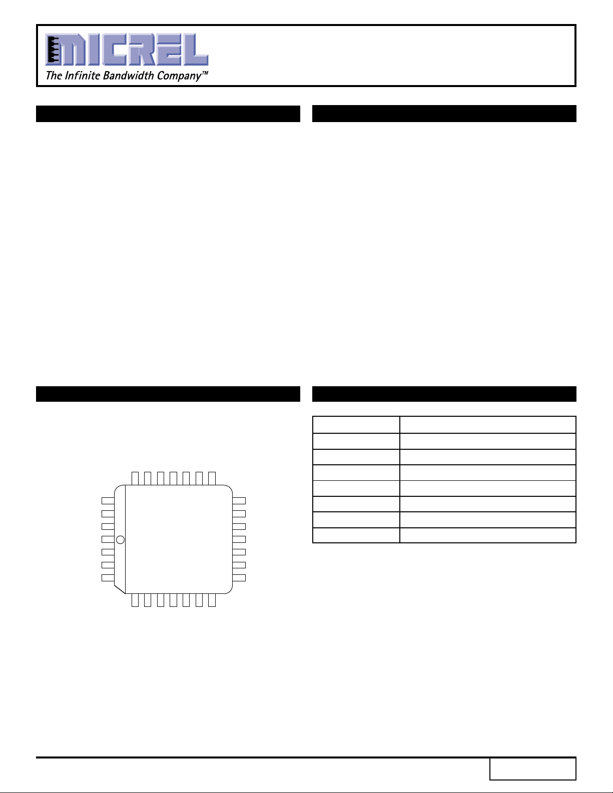
■ Available in 28-pin PLCC package
Outputs (Q)
DESCRIPTION
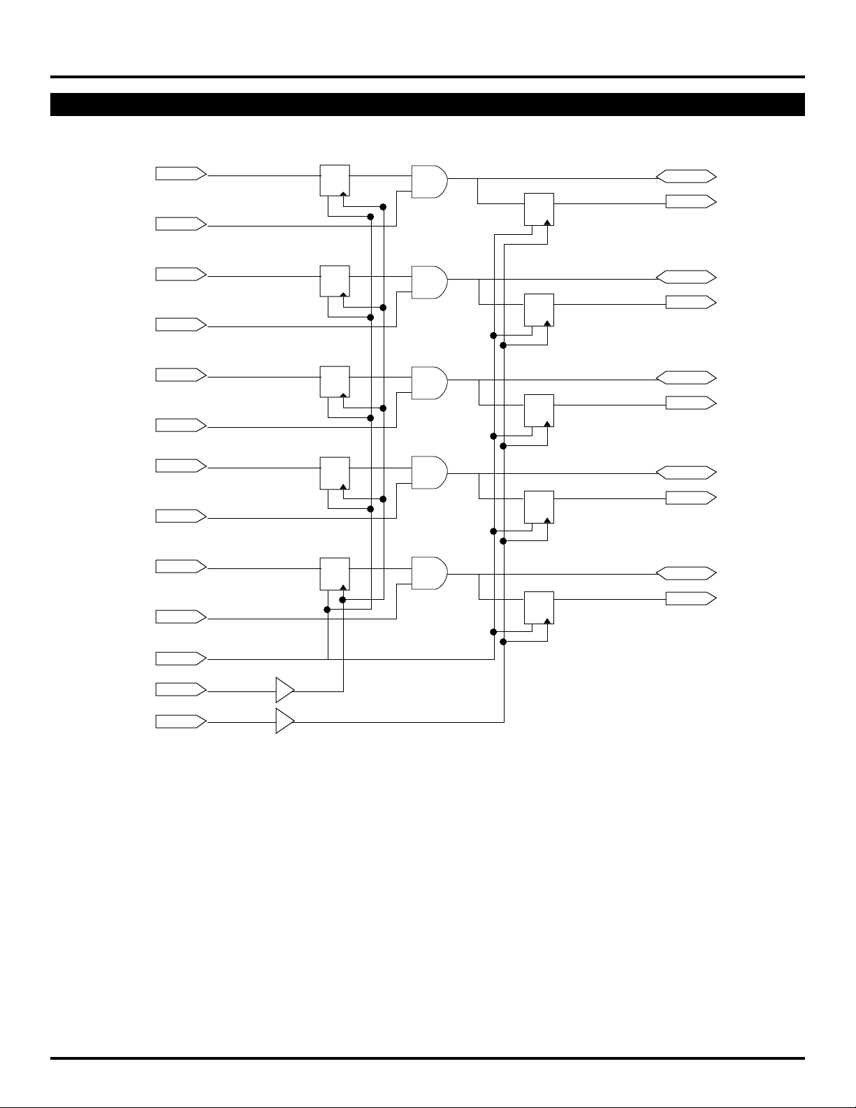
The SY100S891 is a 5-bit registered transceiver
containing five bus transceivers with both transmit and
receive registers. The bus outputs (BUS
specified for driving a 25 ohm bus and the receive outputs
(Q0 – Q4) are specified for driving a 50 ohm line. The
bus outputs have a normal high level output voltage and
a normal low level output voltage when the bus enable
(BUSEN0 – BUSEN4) is high. However, the output is
switched to a cut-off level when a bus-enable is low.
This cut-off level is sufficiently low that a relatively high
impedance is presented to the bus in order to minimize
reflections. There is one bus-enable for each bus driver;
a clock (CLK
registers; and a separate clock (CLK2) which is common
to all five receive registers. Data at the D inputs is clocked
to the Bus register by a positive transition of CLK1 and
data on the bus is clocked into the Receiver register by
a positive transition of CLK2. A high on the Master Reset
clears all registers.
PIN CONFIGURATION PIN NAMES
0 – BUS4) are
1) which is common to all five bus driver
MR
CLK
CLK
V
BUSEN
D
D
EE
Pin Function
3
4
CCA
4
4
3
D
D
BUSEN
BUSEN
25 24 23 22 21 20 19
26
27
2
28
1
1
2
2
3
2
4
1
TOP VIEW
PLCC
J28-1
567891011
0
0
0
1
BUSEN
D
Q
BUSEN
Q
0
BUS
BUS
CCA
V
4
V
18
17
16
15
14
13
12
1
BUS
Q
3
BUS
V
CC
Q
2
BUS
V
CCA
Q
1
3
2
BUSEN0–4 Bus Enable Inputs
D0 – D4 Data Inputs
CLK1 Bus Driver Clock Input
CLK2 Receive Register Clock
MR Master Reset
Q0 – Q4 Bus Receive Outputs
BUS
0–4 Bus Outputs
Rev.: E Amendment: /0
1
Issue Date: August, 1998
Page 2
Micrel
0
2
3
4
2
BLOCK DIAGRAM
SY100S891
BUSEN
BUSEN
BUSEN
BUSEN
BUSEN
D
0
D
1
1
D
2
D
3
D
4
DRQ
C
DRQ
C
DRQ
C
DRQ
C
DRQ
C
25Ω CUTOFF
DRQ
C
25Ω CUTOFF
DRQ
C
25Ω CUTOFF
DRQ
C
25Ω CUTOFF
DRQ
C
25Ω CUTOFF
DRQ
C
50Ω
50Ω
50Ω
50Ω
50Ω
BUS
Q
0
BUS
Q
1
BUS
Q
2
BUS
Q
3
BUS
Q
4
0
1
2
3
4
MR
CLK
CLK
1
2
Page 3

Micrel
SY100S891
DC ELECTRICAL CHARACTERISTICS
VEE = –4.2V to –5.5V unless otherwise specified; VCC = VCCA = GND
Symbol Parameter Min. Typ. Max. Unit Condition
V
CUT Cut-off Bus Output Voltage –2200 –2160 –2100 mV VIN = VIH (Max.) or VIL (Min.) Loading with
25Ω to –2.20V
OH Output HIGH Voltage Bus –1025 –955 –880 mV VIN = VIH (Max.) or VIL (Min.) Loading with
V
OL Output LOW Voltage Bus –1810 –1705 –1620 mV 25Ω to –2.0V
V
V
OHA Output HIGH Voltage Bus –1035 ——mV VIN = VIH (Min.) or VIL (Max.)
VOLA Output LOW Voltage Bus ——–1610 mV
V
OH Output HIGH Voltage Receiver –1025 –955 –880 mV VIN = VIH (Max.) or VIL (Min.) Loading with
VOL Output LOW Voltage Receiver –1810 –1705 –1620 mV 50Ω to –2.0V
OHA Output HIGH Voltage Receiver –1035 ——mV VIN = VIH (Min.) or VIL (Max.)
V
VOLA Output LOW Voltage Receiver ——–1610 mV
VIH Input HIGH Voltage –1165 —–880 mV Guaranteed HIGH Signal for All Inputs
VIL Input LOW Voltage –1810 —–1475 mV Guaranteed LOW Signal for All Inputs
IIL Input LOW Current 0.5 ——µAVIN = VIL (Min.)
IIH Input High Current ——150 µAVIN = VIH (Max.)
IEE Power Supply Current –216 ——mA Inputs Open
CIN Input Pin Capacitance — 4 — pF
OUT Output Pin Capacitance — 5 — pF
C
3
Page 4

Micrel
SY100S891
AC ELECTRICAL CHARACTERISTICS
VEE = –4.2V to –5.5V unless otherwise specified; VCC = VCCA = GND
TA = 0°CTA = +25°CTA = +85°C
Symbol Parameter Min. Typ. Max. Min. Typ. Max. Min. Typ. Max. Unit Condition
PLH Propagation Delay
t
tPHL CLK1 to Bus
PLH Propagation Delay
t
tPHL CLK2 to Q
PLH Propagation Delay
t
tPHL BUSEN to Bus
PLH Propagation Delay
t
tPHL Master Reset to Bus
PLH Propagation Delay
t
tPHL Master Reset to Q
t
S Set-up Time ps
Bus Wrt CLK
D Wrt CLK1 ——400 ——400 ——400
REL Master Reset ——1000 ——1000 ——1000 ps
t
Release Time
H Hold Time ps
t
Bus Wrt CLK2 ——400 ——400 ——400
D Wrt CLK1 ——400 ——400 ——400
r Output Rise Time ps
t
f Output Fall Time ps
t
t
skew Skew (Maximum — 100 ——100 ——100 — ps
Bus
(4)
Q
Bus
(4)
Q
(3)
(3)
difference between
slowest and fastest path)
NOTES:
1. Loaded with 25Ω to –2.0V
2. Loaded with 50Ω to –2.0V
3. 25Ω Load
4. 50Ω Load
(1)
(2)
(1)
(1)
(2)
2 ——400 ——400 ——400
600 1000 1500 600 1000 1500 600 1000 1500 ps
500 800 1200 500 800 1200 500 800 1200 ps
500 800 1200 500 800 1200 500 800 1200 ps
600 1000 1500 600 1000 1500 600 1000 1500 ps
500 800 1200 500 800 1200 500 800 1200 ps
500 — 1000 500 — 1000 500 — 1000
300 — 900 300 — 900 300 — 900
500 — 1000 500 — 1000 500 — 1000
300 — 900 300 — 900 300 — 900
PRODUCT ORDERING CODE
Ordering Package Operating
Code Type Range
SY100S891JC J28-1 Commercial
SY100S891JCTR J28-1 Commercial
4
Page 5

Micrel
28 LEAD PLCC (J28-1)
SY100S891
Rev. 03
MICREL-SYNERGY 3250 SCOTT BOULEVARD SANTA CLARA CA 95054 USA
TEL + 1 (408) 980-9191 FAX + 1 (408) 914-7878 WEB http://www.micrel.com
This information is believed to be accurate and reliable, however no responsibility is assumed by Micrel for its use nor for any infringement of patents or
other rights of third parties resulting from its use. No license is granted by implication or otherwise under any patent or patent right of Micrel Inc.
© 2000 Micrel Incorporated
5
 Loading...