

Page 1
LOW-POWER
4
3
2
8
7
6
L
HEX TTL-TO-PECL
TRANSLATOR
FEATURES
■ Operates from a single +5V supply
■ Differential PECL outputs
■ Function and pinout compatible with Fairchild F100K
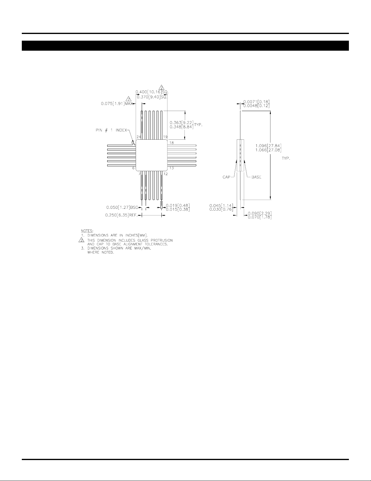
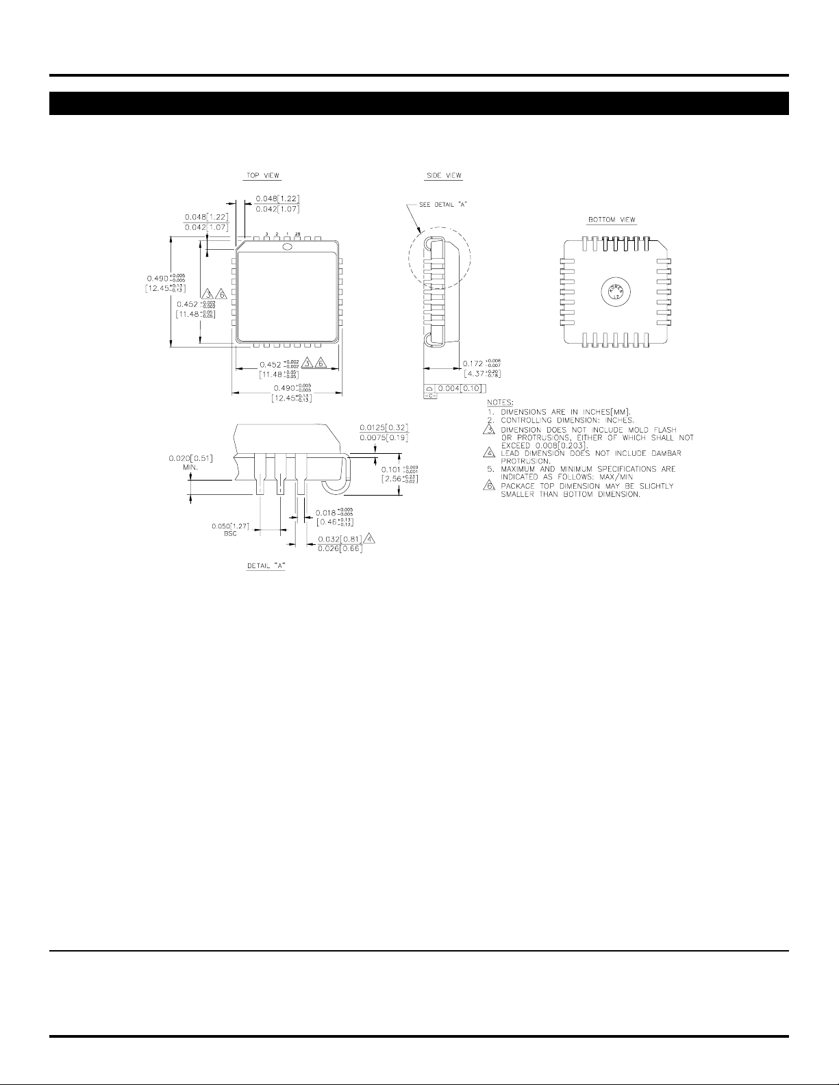
■ Available in 24-pin CERPACK and 28-pin PLCC
packages
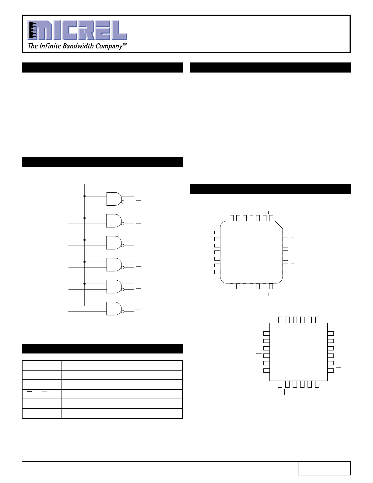
BLOCK DIAGRAM
E
Q
D
0
D
1
D
2
D
3
D
4
D
5
0
Q
0
Q
1
Q
1
Q
2
Q
2
Q
3
Q
3
Q
4
Q
4
Q
5
Q
5
SY100S391
DESCRIPTION
The SY100S391 is a hex TTL-to-PECL translator for
converting TTL logic levels to 100K logic levels. The unique
feature of this translator is the ability to do this translation
using only one +5V supply. The differential outputs allow
each circuit to be used as an inverting/non-inverting translator,
or as a differential line driver. A common enable (E), when
LOW, holds all inverting outputs HIGH and all non-inverting
inputs LOW.
The SY100S391 is ideal for those mixed PECL/TTL
applications which only have a +5V supply available. When
used in the differential mode, the S391, due to its high
common mode rejection, overcomes voltage gradients
between the TTL and PECL ground systems.
PIN CONFIGURATIONS
D
GND TTL
GND PECL
GNDS
GND PECL
D
0
0
D1D
Q
GNDS
2
12
13
14
Top View
15
16
E
17
3
18
PLCC
J28-1
1911201021922823724
5
5
4
D
D
Q
GNDS
1
0
Q
Q1Q
5
6
Q
2
Q
2
V
CCA
1
V
CC
V
CC
2
2
Q
3
2
3
Q
25
4
Q4Q5Q
3
D
E
GND PEC
2
GND TTL
D
GND PECL
D
PIN NAMES
Pin Function
D0 — D5 Data Inputs (TTL)
Q0 — Q5 Data Outputs (PECL)
Q0 — Q5 Inverting Data Outputs (PECL)
4
1
D
5
2
Q
5
3
Top View
Q
5
Q
4
Q
4
Flatpack
4
F24-1
5
6
7248239221021112012
3
3
Q
Q
CC
V
CCA
V
2
Q
D
18
17
16
15
14
13
2
Q
1
D
0
Q
0
Q
0
Q
1
Q
1
E Enable Input (TTL)
CCA VCCO for ECL Outputs
V
Rev.: G Amendment: /0
19
1
Issue Date: July, 1999
Page 2
Micrel
SY100S391
TRUTH TABLE
Inputs Outputs
Dn EQn Qn
HHH L
LHL H
HLL H
LLL H
NOTE:
1. H = High Voltage Level, L = Low Voltage Level
GUARANTEED OPERATING CONDITIONS
Symbol Rating Value Unit
T
A Operating Temperature ˚C
Commercial 0 to +85
CC Supply Voltage +4.5 to +5.5 V
V
NOTE:
1. Do not exceed.
LOGIC SYMBOL
D
0
E
Q0 Q0Q1 Q1Q2 Q2Q3 Q3Q4 Q4Q5 Q
ABSOLUTE MAXIMUM RATINGS
Symbol Rating Value Unit
(1)
— TTL Input Voltage
— TTL Input Current
— PECL Output Current –50 V
— V
Tstore Storage Temperature –65 to +150 ˚C
T
J Max. Junction Temp. ˚C
NOTES:
1. Permanent device damage may occur if ABSOLUTE MAXIMUM RATINGS
are exceeded. This is a stress rating only and functional operation is not
implied at conditions other than those detailed in the operational sections
of this data sheet. Exposure to ABSOLUTE MAXIMUM RATlNG conditions
for extended periods may affect device reliability.
2. Either voltage limit or current limit is siffucient to protect inputs.
D
1
D
2
D
3
(2)
(2)
D
(1)
–0.5 to +7.0 V
–30 to +5.0 V
(DC Output HIGH)
CC Pin Potential to –0.5 to +7.0 V
Ground Pin
Ceramic +175
Plastic +150
4
D
5
5
TTL-TO-PECL DC ELECTRICAL CHARACTERISTICS
(1)
VCC = +5.0V ± 10%; GND = 0V
Symbol Parameter Min. Typ. Max. Unit Condition
VOH Output HIGH Voltage VCC –1025 VCC –955 VCC –870 mV VIN = VIH (Max.) or VIL (Min.)
VOL Output LOW Voltage VCC –1890 VCC –1705 VCC –1620 Loading with 50Ω to VCC –2V
VOHC Output HIGH Voltage VCC –1035 —— mV VIN = VIH (Min.) or VIL (Max.)
Corner Point High Loading with 50Ω to VCC –2V
VOLC Output LOW Voltage ——VCC –1610 mV
Corner Point Low
VIH Input HIGH Voltage 2.0 — 5.0 V Over VTTL, VEE, TA Range
VIL Input LOW Voltage 0 — 0.8 V Over VTTL, VEE, TA Range
IIH Input HIGH Current ——10 µAVIN = +2.7V
Breakdown Current ——100 µAVIN = +5.5V, VCC = Max.
IIL Input LOW Current Dn ——–0.8 mA VIN = +0.5V
E –4.2
VCD Input Clamp Diode Voltage ——–1.2 V IIN = –18mA
ICC VCC Supply Current 25 — 69 mA Inputs Open
NOTE:
1. The specified limits represent the "worst case" value for the parameter. Since these values normally occur at the temperature extremes, additional noise
immunity and guardbanding can be achieved by decreasing the allowable system operating ranges. Conditions for testing shown in the tables are chosen
to guarantee operation under "worst case" conditions.
2
Page 3
Micrel
AC ELECTRICAL CHARACTERISTICS
CERPACK AND PLCC
VCC = +5.0V ± 10%
TA = 0°CTA = +25°CTA = +85°C
Symbol Parameter Min. Max. Min. Max. Min. Max. Unit Condition
PLH Propagation Delay 400 1400 400 1400 400 1400 ps
t
tPHL Data and Enable to Output
TLH Transition Time 350 1700 350 1700 350 1700 ps
t
tTHL 20% to 80%, 80% to 20%
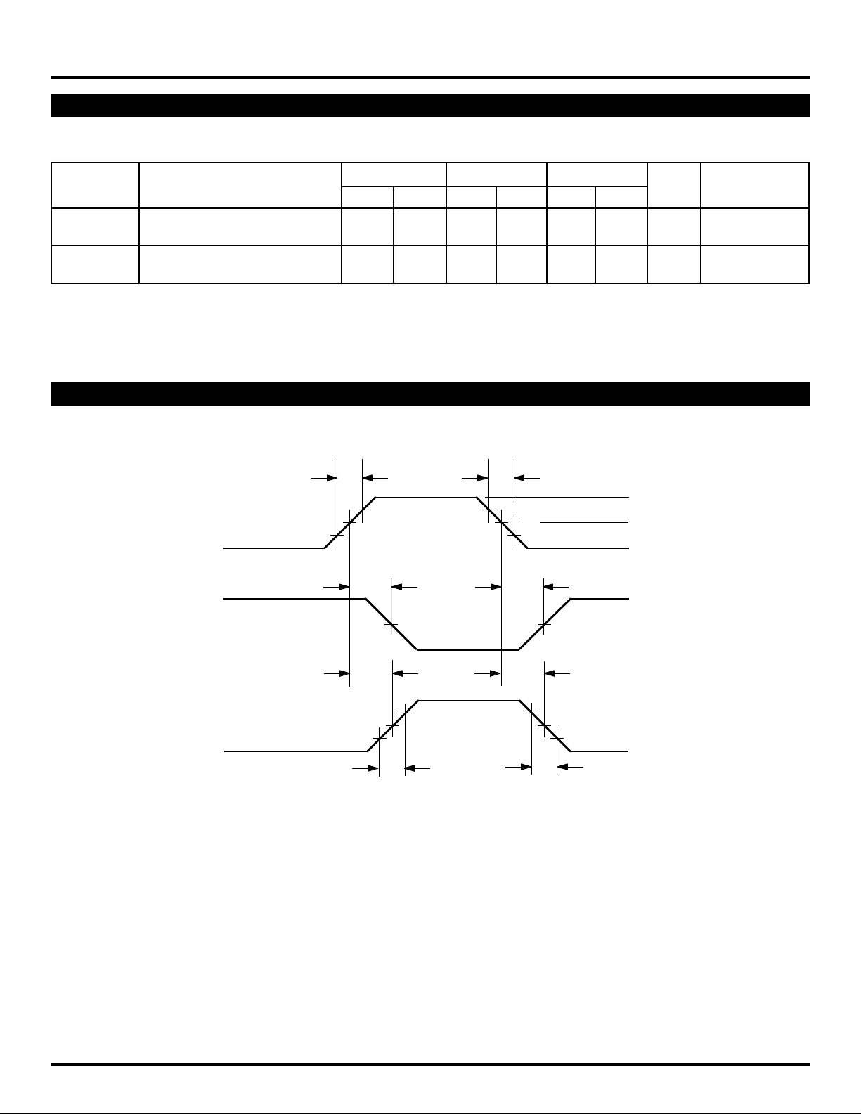
TIMING DIAGRAM
SY100S391
INPUT
OUTPUT
2.5 ± 0.3ns 2.5 ± 0.3ns
90%
50%
10%
t
t
PHL
PLH
COMPLEMENT
50%
t
TRUE
PLH
t
TLH
Propagation Delay and Transition Times
t
PHL
t
THL
80%
50%
20%
3.0V
1.5V
0V
3
Page 4
Micrel
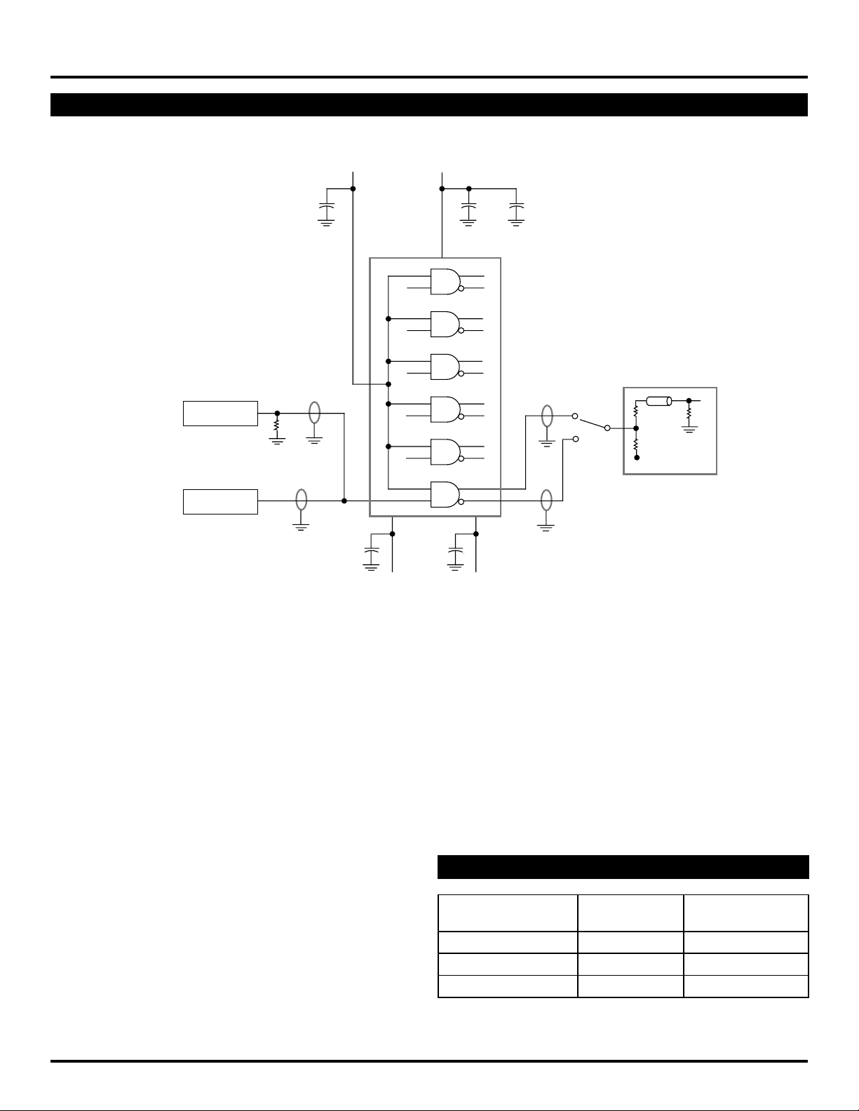
TEST CIRCUIT
SY100S391
SCOPE
CHAN A
PULSE
GENERATOR
V
IH
0.1µF
L
1
R
T
0.1µF
GNDTTL
2.5µF
0.1µF 0.1µF
L
2
50
100
–4V
L
3
S/H
R
PECL
TERMINATOR
NET
T
GNDPECL
V
CC
PRODUCT ORDERING CODE
Ordering Package Operating
Code Type Range
SY100S391FC F24-1 Commercial
SY100S391JC J28-1 Commercial
SY100S391JCTR J28-1 Commercial
4
Page 5
Micrel
24 LEAD CERPACK (F24-1)
SY100S391
Rev. 03
5
Page 6
Micrel
28 LEAD PLCC (J28-1)
SY100S391
Rev. 03
MICREL-SYNERGY 3250 SCOTT BOULEVARD SANTA CLARA CA 95054 USA
TEL + 1 (408) 980-9191 FAX + 1 (408) 914-7878 WEB http://www.micrel.com
This information is believed to be accurate and reliable, however no responsibility is assumed by Micrel for its use nor for any infringement of patents or
other rights of third parties resulting from its use. No license is granted by implication or otherwise under any patent or patent right of Micrel Inc.
© 2000 Micrel Incorporated
6
 Loading...