

Page 1
3-BIT SCANNABLE
REGISTER
SY10E212
SY100E212
FEATURES
■ Scannable version E112 driver
■ Extended 100E VEE range of –4.2V to –5.5V
■ 1025ps max. CLK to Output
■ Dual differential outputs
■ Master Reset
■ Internal 75KΩ input pull-down resistors
■ Fully compatible with industry standard 10KH,
100K ECL levels
■ Fully compatible with Motorola MC10E/100E212
■ Available in 28-pin PLCC package
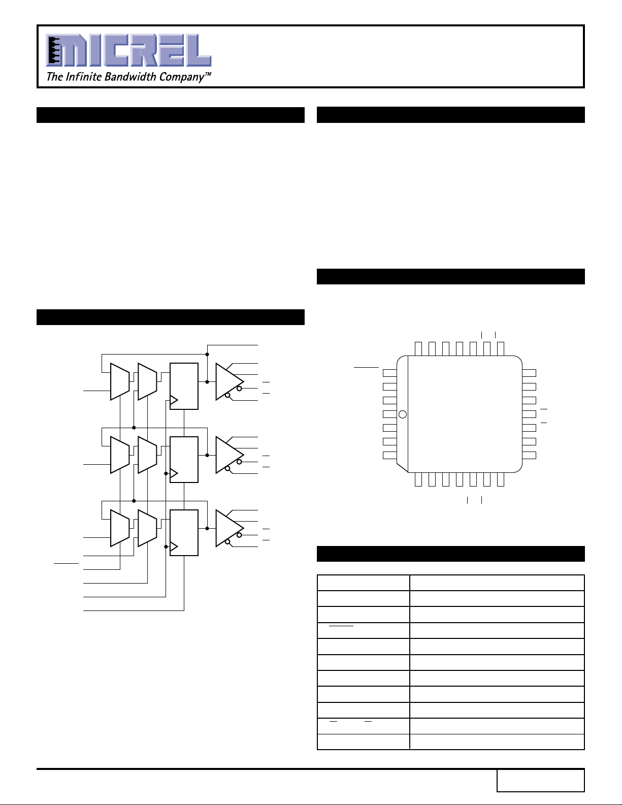
BLOCK DIAGRAM
S-OUT
Q
D
Q
D
2
D
Q
D
1
2b
Q
2a
Q
2a
Q
2b
Q
1b
Q
1a
Q
1a
Q
1b
DESCRIPTION
The SY10/100E212 are scannable registered ECL
drivers typically used as fan-out memory address drivers
for ECL cache driving. In a VLSI array-based CPU design,
use of the E212 allows the user to conserve array output
cell functionality and also output pins.
The input shift register is designed with control logic
which greatly facilitates its use in boundary scan
applications.
PIN CONFIGURATION
2b
CCO
Q2a
V
S-OUT
Q
18
Q2b
17
Q2a
16
VCC
15
Q1b
14
Q1a
13
Q1b
12
Q1a
LOAD
CLK
D
VEE
D1
D0
S-IN
NC
SHIFT
MR
25
24 23 22 21 20 19
26
27
28
2
1
2
3
4
TOP VIEW
PLCC
J28-1
567891011
D
S-IN
LOAD
SHIFT
CLK
MR
NC
CCO
Q0b
Q0a
Q0a
Q
D
Q
0
0b
Q
0a
Q
0a
Q
0b
V
Q0b
VCCO
PIN NAMES
Pin Function
D0 – D2 Data Inputs
S-IN Scan Input
LOAD LOAD/HOLD Control
SHIFT Scan Control
CLK Clock
MR Master Reset
S-OUT Scan Output
Q[0:2]a, Q[0:2]b True Outputs
Q[0:2]a, Q[0:2]b Inverting Outputs
CCO VCC to Output
V
Rev.: C Amendment: /1
1
Issue Date: February, 1998
Page 2
SY10E212
Micrel
SY100E212
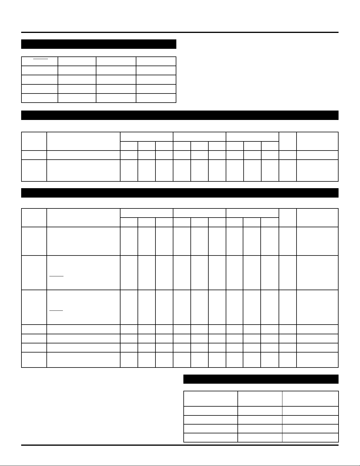
TRUTH TABLE
LOAD SHIFT MR Mode
L L L Load
H L L Hold
X H L Shift
X X H Reset
DC ELECTRICAL CHARACTERISTICS
VEE = VEE (Min.) to VEE (Max.); VCC = VCCO = GND
TA = 0°CTA = +25°CTA = +85°C
Symbol Parameter Min. Typ. Max. Min. Typ. Max. Min. Typ. Max. Unit Condition
IIH Input HIGH Current — — 150 — — 150 — — 150 µA—
EE Power Supply Current mA —
I
10E — 80 96 — 80 96 — 80 96
100E — 80 96 — 80 96 — 92 110
AC ELECTRICAL CHARACTERISTICS
VEE = VEE (Min.) to VEE (Max.); VCC = VCCO = GND
TA = 0°CTA = +25°CTA = +85°C
Symbol Parameter Min. Typ. Max. Min. Typ. Max. Min. Typ. Max. Unit Condition
PLH Propagation Delay to Output ps —
t
tPHL CLK 575 800 1025 575 800 1025 575 800 1025
MR 575 800 1025 575 800 1025 575 800 1025
CLK to S-OUT 575 800 1025 575 800 1025 575 800 1025
t
S Set-up Time ps —
D 175 25 — 175 25 — 175 25 —
SHIFT 150 –50 — 150 –50 — 150 –50 —
LOAD 225 50 — 225 50 — 225 50 —
S-IN 150 –50 — 150 –50 — 150 –50 —
H Hold Time ps —
t
D 250 25 — 250 25 — 250 25 —
SHIFT 300 100 — 300 100 — 300 100 —
LOAD 225 0 — 225 0 — 225 0 —
S-IN 300 100 — 300 100 — 300 100 —
tRR Reset Recovery 600 350 — 600 350 — 600 350 — ps —
tskew Within-Device Skew — 100 — — 100 — — 100 — ps 1
tskew Within-Gate Skew — 50 — — 50 — — 50 — ps 2
r Rise/Fall Times 275 425 650 275 425 650 275 425 650 ps —
t
tf 20% to 80%
NOTES:
1. Within-device skew is defined as identical transitions on similar paths
through a device.
2. Within-gate skew is defined as the difference in delays between various
outputs of a gate when driven from the same input.
PRODUCT ORDERING CODE
Ordering Package Operating
Code Type Range
SY10E212JC J28-1 Commercial
SY10E212JCTR J28-1 Commercial
SY100E212JC J28-1 Commercial
SY100E212JCTR J28-1 Commercial
2
Page 3
Micrel
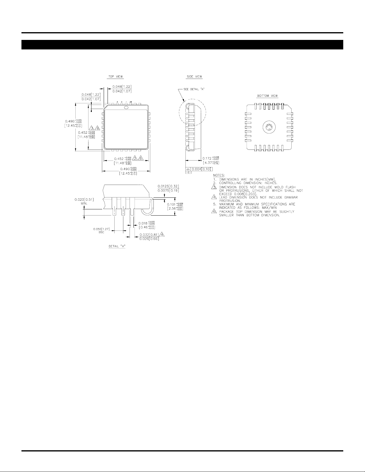
28 LEAD PLCC (J28-1)
SY10E212
SY100E212
Rev. 03
3
Page 4

Micrel
SY10E212
SY100E212
MICREL-SYNERGY 3250 SCOTT BOULEVARD SANTA CLARA CA 95054 USA
TEL + 1 (408) 980-9191 FAX + 1 (408) 914-7878 WEB http://www.micrel.com
This information is believed to be accurate and reliable, however no responsibility is assumed by Micrel for its use nor for any infringement of patents or
other rights of third parties resulting from its use. No license is granted by implication or otherwise under any patent or patent right of Micrel Inc.
© 2000 Micrel Incorporated
4
 Loading...