

Page 1
(÷1, ÷2/3) OR (÷2, ÷4/6)
CLOCK GENERATION CHIP
ClockWorks™
SY100S838
SY100S838L
FEATURES
■ 3.3V and 5V power supply options
■ 50ps output-to-output skew
■ Synchronous enable/disable
■ Master Reset for synchronization
■ Internal 75KΩ input pull-down resistors
■ Available in 20-pin SOIC package
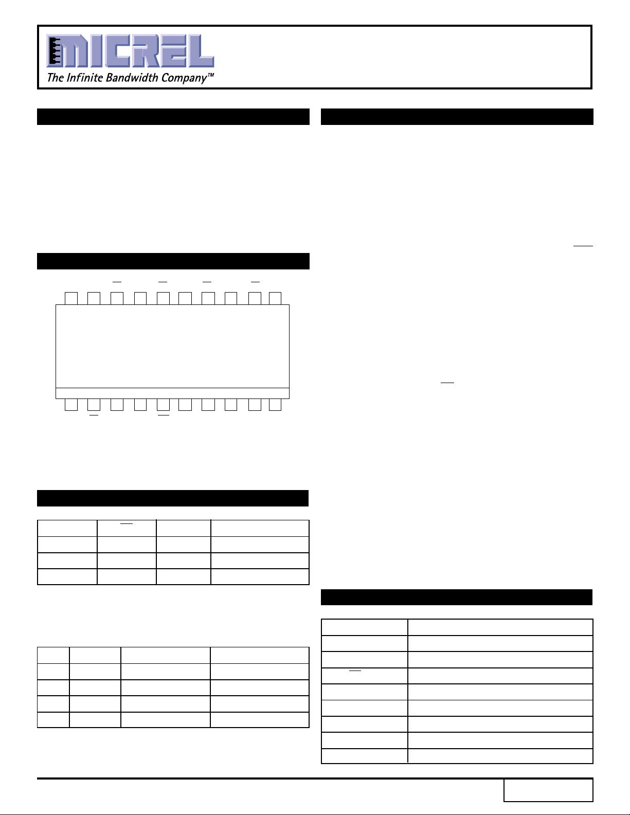
PIN CONFIGURATION
Q
VCCQ0Q0Q
20 19
12345678910
VCCEN DIVSEL CLK CLK VBBMR V
18 17 16 15 14 13
1
TOP VIEW
1
SOIC
Z20-1
Q2Q
Q
3
2
Q3V
EE
12 11
CC
NC F
SEL
TRUTH TABLE
CLK EN MR Function
Z L L Divide
ZZ H L Hold Q0–3
X X H Reset Q0–3
NOTES:
Z = LOW-to-HIGH transition
ZZ = HIGH-to-LOW transition
FSEL DIVSEL Q0, Q1 OUTPUTS Q2, Q3 OUTPUTS
L L Divide by 2 Divide by 4
L H Divide by 2 Divide by 6
H L Divide by 1 Divide by 2
H H Divide by 1 Divide by 3
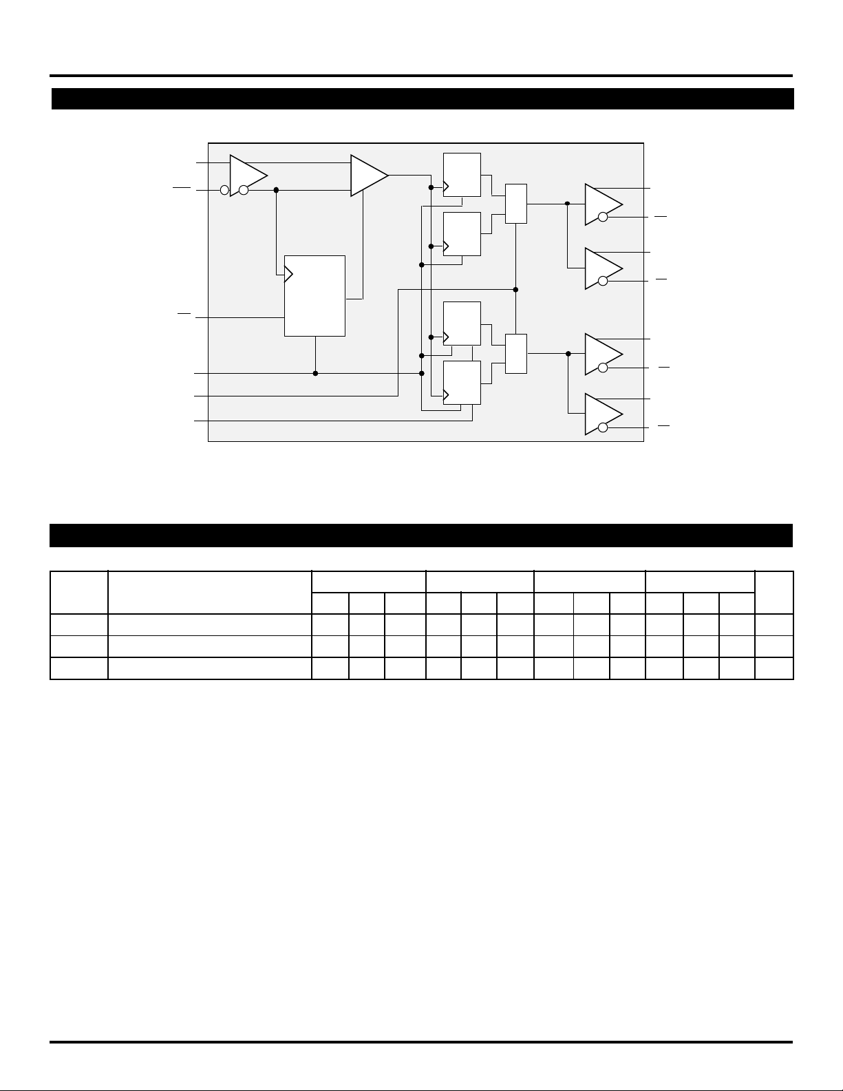
DESCRIPTION
The SY100S838/L is a low skew (÷1, ÷2/3) or (÷2, ÷4/
6) clock generation chip designed explicitly for low skew
clock generation applications. The internal dividers are
synchronous to each other, therefore, the common output
edges are all precisely aligned. The devices can be driven
by either a differential or single-ended ECL or, if positive
power supplies are used, PECL input signal. In addition,
by using the VBB output, a sinusoidal source can be ACcoupled into the device. If a single-ended input is to be
used, the VBB output should be connected to the CLK
input and bypassed to ground via a 0.01µF capacitor.
The VBB output is designed to act as the switching
reference for the input of the SY100S838/L under singleended input conditions. As a result, this pin can only
source/sink up to 0.5mA of current.
The Function Select (FSEL) input is used to determine
what clock generation chip function is. When FSEL input
is LOW, SY100S838/L functions as a divide by 2 and by
4/6 clock generation chip. However, if FSEL input is HIGH,
it functions as a divide by 1 and by 2/3 clock chip.
The common enable (EN) is synchronous so that the
internal dividers will only be enabled/disabled when the
internal clock is already in the LOW state. This avoids
any chance of generating a runt clock pulse on the
internal clock when the device is enabled/disabled as
can happen with an asynchronous control. An internal
runt pulse could lead to losing synchronization between
the internal divider stages. The internal enable flip-flop is
clocked on the falling edge of the input clock, therefore,
all associated specification limits are referenced to the
negative edge of the clock input.
Upon start-up, the internal flip-flops will attain a random
state; the master reset (MR) input allows for the
synchronization of the internal dividers, as well as for
multiple SY100S838/Ls in a system.
PIN NAMES
Pin Function
CLK Differential Clock Inputs
FSEL Function Select Input
EN Synchronous Enable
MR Master Reset
VBB Reference Output
Q0, Q1 Differential ÷1 or ÷2 Outputs
Q2, Q3 Differential ÷2/3 or ÷4/6 Outputs
DIVSEL Frequency Select Input
Rev.: E Amendment: /1
1
Issue Date: August, 1998
Page 2
Micrel
K
K
BLOCK DIAGRAM
ClockWorks™
SY100S838
SY100S838L
CL
CL
EN
MR
F
SEL
DIVSEL
R
DC ELECTRICAL CHARACTERISTICS
(1)
÷
1
Q
1
÷
2
÷
2
or
÷
3
÷
4
or
÷
6
0
1
0
0
Q
0
Q
1
Q
1
Q
2
Q
2
Q
3
Q
3
VEE = VEE (Min.) to VEE (Max.); VCC = GND
A = –40°CTA = 0°CTA = +25°CTA = +85°C
T
Symbol Parameter Min. Typ. Max. Min. Typ. Max. Min. Typ. Max. Min. Typ. Max. Unit
IEE Power Supply Current 35 50 65 35 50 65 35 50 65 35 54 75 mA
VBB Output Reference Voltage -1.38 — -1.26 -1.38 — -1.26 -1.38 — -1.26 -1.38 — -1.26 V
I
IH Input High Current ——150 ——150 ——150 ——150 µA
NOTE:
1. Parametric values specified at: 5 volt Power Supply Range 100S838 Series: -4.2V to -5.5V.
3 volt Power Supply Range 100S838L Series -3.0V to -3.8V.
2
Page 3

Micrel
ClockWorks™
SY100S838
SY100S838L
AC ELECTRICAL CHARACTERISTICS
(1)
VEE = VEE (Min.) to VEE (Max.); VCC = GND
TA = –40°CTA = 0°CTA = +25°CTA = +85°C
Symbol Parameter Min. Typ. Max. Min. Typ. Max. Min. Typ. Max. Min. Typ. Max. Unit
fMAX Maximum Toggle Frequency 1000 ——1000 ——1000 ——1000 ——MHz
PLH Propagation Delay to Output ps
t
t
PHL CLK ➝ Output (Diff.) 950 — 1150 950 — 1150 970 — 1170 1050 — 1250
CLK
➝ Output (S.E.) 900 — 1200 900 — 1200 920 — 1220 1000 — 1300
MR ➝ Q 600 — 900 600 — 900 600 — 900 600 — 900
tskew Within-Device Skew
Part-to-Part Q0 — Q3 (Diff.) ——200 ——200 ——200 ——200
S Set-up Time EN ➝ CLK 300 150 — 300 150 — 300 150 — 300 150 — ps
t
tH Hold Time CLK ➝ EN 400 150 — 400 150 — 400 150 — 400 150 — ps
VPP Minimum Input Swing
VCMR Common Mode Range
tRR Reset Recovery Time ——100 ——100 ——100 ——100 ps
t
PW Minimum Pulse Width CLK 800 ——800 ——800 ——800 —— ps
tr Output Rise/Fall Times Q 280 — 550 280 — 550 280 — 550 280 — 550 ps
tf (20% —80%)
NOTES:
1. Parametric values specified at: 5 volt Power Supply Range 100S838 Series: -4.2V to -5.5V.
2. Skew is measured between outputs under identical transitions.
3. Minimum input swing for which AC parameters are guaranteed. The device will function reliably with differential inputs down to 100mV.
4. The CMR range is referenced to the most positive side of the differential input signal. Normal operation is obtained if the HIGH level falls within the specified
range and the peak-to-peak voltage lies between VPP (min) and 1.0V. The lower end of the CMR range is dependent on VEE and is equal to VEE +1.65V.
(2)
Q0 — Q3 ——50 ——50 ——50 ——50 ps
DIVSEL ➝ CLK 300 ——300 ——300 ——300 ——
CLK ➝ DIVSEL 400 200 — 400 200 — 400 200 — 400 200 —
(3)
CLK 250 ——250 ——250 ——250 ——mV
(4)
CLK (4) — -0.55 (4) — -0.55 (4) — -0.55 (4) — -0.55 V
MR 700 ——700 ——700 ——700 ——
3 volt Power Supply Range 100S838L Series -3.0V to -3.8V.
TIMING DIAGRAM
CLK
Q (÷1)
Q (÷2)
Q (÷3)
Q (÷4)
Q (÷6)
PRODUCT ORDERING CODE
Ordering Package Operating VEE Range
Code Type Range (V)
SY100S838ZC Z20-1 Commercial -4.2 to -5.5
SY100S838ZCTR Z20-1 Commercial -4.2 to -5.5
SY100S838LZC Z20-1 Commercial -3.0 to -3.8
SY100S838LZCTR Z20-1 Commercial -3.0 to -3.8
Ordering Package Operating VEE Range
Code Type Range (V)
SY100S838ZI Z20-1 Industrial -4.2 to -5.5
SY100S838ZITR Z20-1 Industrial -4.2 to -5.5
SY100S838LZI Z20-1 Industrial -3.0 to -3.8
SY100S838LZITR Z20-1 Industrial -3.0 to -3.8
3
Page 4

Micrel
20 LEAD SOIC .300" WIDE (Z20-1)
ClockWorks™
SY100S838
SY100S838L
Rev. 03
MICREL-SYNERGY 3250 SCOTT BOULEVARD SANTA CLARA CA 95054 USA
TEL + 1 (408) 980-9191 FAX + 1 (408) 914-7878 WEB http://www.micrel.com
This information is believed to be accurate and reliable, however no responsibility is assumed by Micrel for its use nor for any infringement of patents or
other rights of third parties resulting from its use. No license is granted by implication or otherwise under any patent or patent right of Micrel Inc.
© 2000 Micrel Incorporated
4
 Loading...