

Page 1

Digital Broadcast Reception LSI
MN88413
Channel Decoder LSI for Digital Satellite Broadcast Reception
■ Overview
The MN88413 is a channel decoder LSI that integrates functions for digital satellite communications and broadcast
reception on a single chip.
The MN88413 supports both the Digital Video Broadcast (DVB) and the Digital Satellite System (DSS
It also supports a variable transport rate that can be set under program control using a fixed system clock frequency and
can implement a channel decoder with a minimal number of external components.
■ Features
•
Can be used in systems conforming to DVB, in US DIRECTV
communication systems.
•
Integrates a 2-channel A/D converter, a variable rate QPSK demodulator, and forward error correction
(FEC) on a single chip.
•
Supports transfer rates from 1 Mbps to 90 Mbps.
•
On-chip I/Q baseband signal offset voltage circuit and on-chip reference voltage circuit for the A/D and D/A converters.
•
On-chip PLL circuit
•
BER monitor function
2
•
I
C bus master circuit for tuner control
•
Supports LNB control clock and DiSEqC 1.0/1.1 and can output DiSEqC messages.
•
General-purpose input and output ports
•
On-chip boundary scan test circuit conforming to IEEE 1149.1
systems, and in single carrier per channel (SCPC)
) specifications.
■ Applications
•
Digital satellite broadcast receivers
Note: DSS and DIRECTV are registered trademarks of DIRECTV, Inc.
1
Page 2
MN88413 Digital Bloadcast Reception LSI
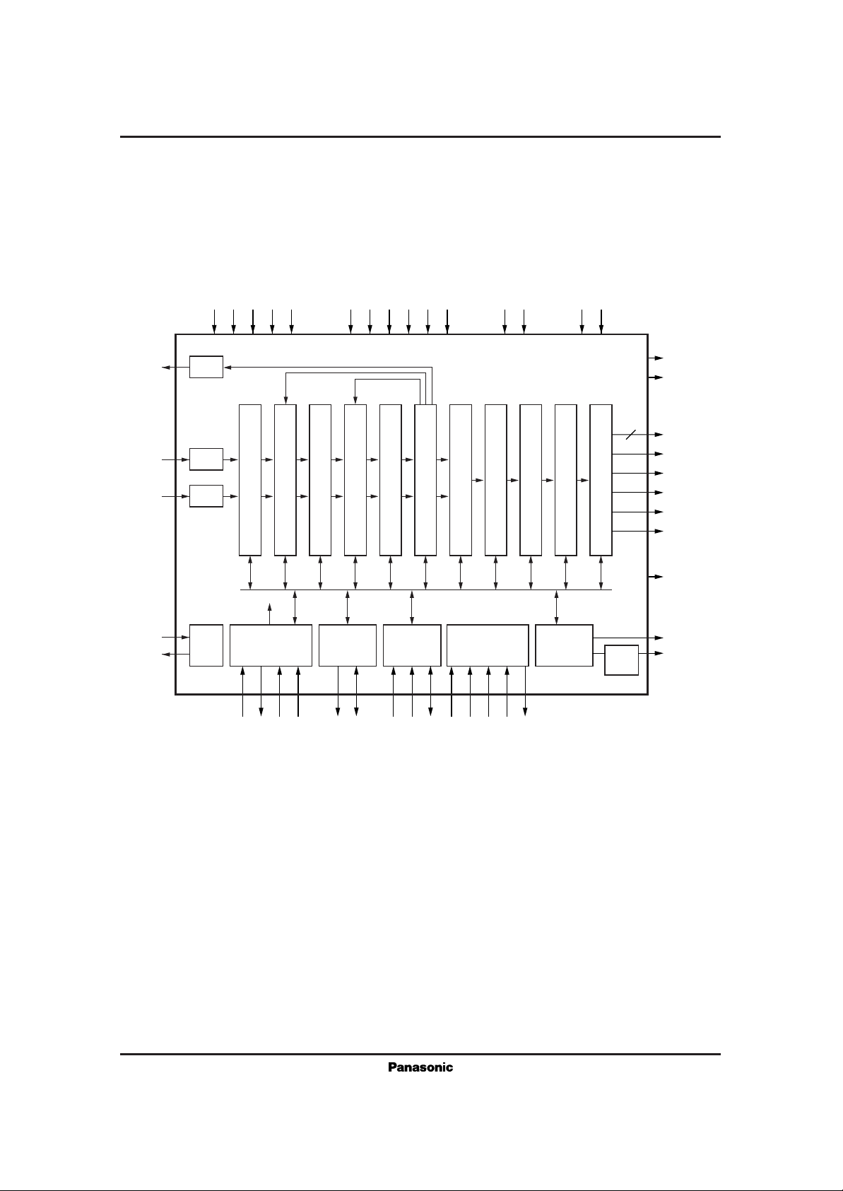
■ Block Diagram
VSS0-6
VDD0-6
VSSA0-2
VDDA1-2
VSSC0-19
ADVRT
ADVRB
IVRM
QVRM
DAVR
DAIR
TIN3-7
TEST0-2
NRST
SEL
QIN
PLL0-2
CPO
DACAGC
ADCIIN
ADC
PLL
Digital AFC
Offset canceler
Clock
reproduction
XI
XO
CKI
Rate converter
Bandwidth limiter
I2C I/F
(Master)
MSCL
CSEL0-1
MSDA
Roll-off filter
QPSK demodulator
I2C I/F
SCL
SDA
SADR0-1
detector
Viterbi decoder
Frame synchronization
TAP
controller
(JTAG)
TDI
TCK
TMS
TRST
De-interleaver
Reed-Solomon decoder
LNB
controller
TDO
NERRF
FSYNC
DO0-7
DEN
BYTCK
PSYNC
NPERR
Energy dispersal decoder
DAC
SCK
OP0-2
LNBCK
LNB
2
Page 3

Digital Bloadcast Reception LSI MN88413
■ Pin Assignment
TCK
TMS
TRST
VSSC14
SCK
DO7
VDD4
VSSC13
VSS4
DO6
DO5
DO4
VSSC12
DO3
DO2
DO1
VDD3
VSSC11
VSS3
DO0
BYTCK
VSSC10
DEN
PSYNC
NPERR
75747372717069686766656463626160595857565554535251
TDI
TDO
TIN3
VSSC15
TIN4
VSS5
VDD5
VSSC16
TIN5
TIN6
TIN7
OP0
VSSC17
OP1
OP2
LNBCK
CKO
VSSC18
VSS6
VDD6
XO
VSSC19
XI
CSEL0
CSEL1
76
77
78
79
80
81
82
83
84
85
86
87
88
89
90
91
92
93
94
95
96
97
98
99
100
123456789
101112131415161718192021222324
25
50
49
48
47
46
45
44
43
42
41
40
39
38
37
36
35
34
33
32
31
30
29
28
27
26
PLL2
PLL1
PLL0
VSSC9
VDD2
VSS2
NERRF
VSSC8
FSYNC
SEL
NRST
SDA
VSSC7
SCL
VDD1
VSS1
MSDA
VSSC6
MSCL
SADR1
SADR0
VSSC5
TEST2
TEST1
TEST0
CKI
VSS0
VDD0
VSSC0
VSSA0
CPO
VDDA0
DAVR
VSSC1
LNB
DAIR
AGC
VSSC2
IIN
VSSA1
VDDA1
IVRM
VSSC3
QVRM
ADVRT
ADVRB
QIN
VSSC4
VSSA2
VDDA2
3
Page 4

MN88413 Digital Bloadcast Reception LSI
■ Specifications Overview
•
QPSK demodulator
Data rate : 1 Mbps to 90 Mbps
A/D converter resolution : 6 bits
Linearity error : ±0.5 LSB (typical)
Differential linearity error : ±0.5 LSB (typical)
Input voltage level : 1.5 V [p-p] (typical) [On-chip self-bias circuit]
Roll-off rate : Switchable between the DVB and the DSS
AFC range : ± (<symbol rate>/8)
Synchronization establishment time : 100 ms or less.
D/A converter used for LNB/AFC and AGC
Resolution : 8 bits
Linearity error : ±0.5 LSB (typical)
Differential linearity error : ±0.5 LSB (typical)
Output voltage level : 1.0 V [p-p] (typical) [0.0 V to 1.0 V]
specifications.
•
Viterbi decoder : Switchable between the DVB and the DSS
specifications.
: Automatic detection of encoding ratios in the range 1/2 to 7/8.
: Auto-synchronous operation
•
Frame synchronization detection, De-interleaver, Reed-Solomon decoding, and Energy dispersal
: Switchable between the DVB and the DSS
•
PLL circuit : Reference clock input frequency: 4 MHz to 30 MHz
•
CPU interface : I2C bus interface
•
Supply voltage : 3.3 V ±0.165 V
•
Power dissipation : 990 mW (typical) [at VDD = 3.3 V, 60 Mbps, R = 7/8]
•
Package : QFP100-P-1818B (18 × 18 mm)
specifications.
4
Page 5

Digital Bloadcast Reception LSI MN88413
■ System Application Example
Antenna
12 GHz
950 MHz ∼
1.45 GHz
Microcontroller
MN1870877
BPFAGC BPF
2
C host interface
I
■ Package Dimensions (units: mm)
•
QFP100-P-1818B
22.90±0.20
18.00±0.10
Tuner
1.45 GHz ∼
1.95 GHz
5175
Quadrature
detector
AN8921SB
500 MHz
(1.20)
IIN
QIN
AGC
XI
XO
LNB control
I2C master
2
I
DO0-7
BYTCK
PSYNC
NPERR
MN88413
C interface
DEN
SCK
8
To the descrambler
76
(1.20)
50
22.90±0.20
18.00±0.10
26100
125
0.65
0.15
Seating plane
0.30±0.05
2.85max.
2.45±0.20
0.15±0.05
1.30±0.20
0.10±0.10
(2.45)
0 to 10°
5
 Loading...