

Page 1
For Information Equipment
MN8390-C
LCD Panel Source Driver
Overview
The MN8390-C is for displaying an analog video signal on
a TFT color liquid crystal display panel in such applications
as LCD television sets and video cameras.
Features
Lower power consumption and reduced EMI emissions
owing to digital 3.0 volt power supply and analog 5.0
volt power supply
Broad dynamic range of 4.6 V (for power supply
voltage of 5.0 V)
Low discrepancies between output pins: ±20 mV (typ.)
240 output channels
Support for striped and delta panel layouts by switching
analog (R, G, B) signals
Support for sequential sampling mode (with CLK1 to
CLK3 inputs)
Support for serial cascade connections
Automatic clock suspension after reading specified
amount of data
Choice of shift register shift directions (right/left)
Applications
LCD television sets and video cameras
Page 2
MN8390-C For Information Equipment
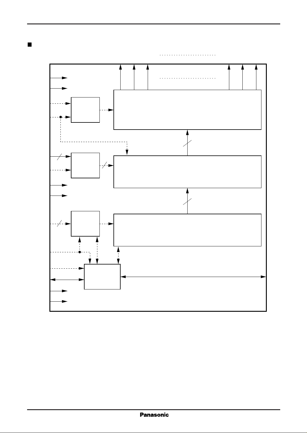
Block Diagram
QA1
QB1
QC1
V
DD2
V
SS2
QA80
QB80
QC80
VBS
OE
VA,VB,
VC
D1
V
DD1
V
SS1
CLK1,
CLK2,
CLK3
MOD
RL
STHR
3
3
Bias
control circuit
Analog
multiplexer
Clock
generator
circuit
Shift register
control circuit
Output buffer
240
3
Two sample-and-hold circuits
240
Bidirectional 240-bit shift register
STHL
TEST1
TEST2
Page 3

For Information Equipment MN8390-C
Pin Descriptions
Pin No. Symbol Pin Name I/O Function Description
99 to 102 STHR Shift data I/O I/O These are I/O pins for the bidirectional shift register.
21 to 24 STHL The RL pin controls their I/O directions.
RL
H
L
(1) Input
The pins provide input data to the shift register's first
stage. The shift register reads in this data at the rising
edge of the CLK1 signal.
(2) Output
In a cascade connection, the pins provide the data for
the synchronizing output stage synchronized with the
rising edge of the CLK1 signal.
27 to 30 RL Shift direction I This pin controls the shift direction for the
control bidirectional shift register.
RL="H" : QA1→ QB1→ QC1→ → QC80
RL="L" : QC80→ QB80→ QA80→ → QA1
42 to 45 CLK1 to 3 Clock input I These pins provide the shift clock signals that the
37 to 40 sample-and-hold circuits use to generate the data for
32 to 35 the LCD drive output pins (QA1-QC80).
The following lists the relationships between these
clock signals and the output pins.
CLK1 RL="H": QA1 to QA80
CLK2: QB1 to QB80
CLK3 RL="H": QC1 to QC80
70 to 73 OE Output enable I At each rising edge of this signal, the MN8390-C
switches between its two sample-and-hold circuits
and initiates output of new data. When the outputs
reach the drive potential, the MN8390-C
automatically reduces the drive power, but maintains
the outputs at the drive potential.
47 to 50 D1 Analog signal I This pin controls the mapping between the three
swiching analog inputs (VA, VB, and VC) and the drive
outputs (QA, QB, and QC).
D1
L
H
STHR
Input
Output
STHL
Output
Input
RL="L": QC1 to QC80
RL="L": QA1 to QA80
Input
VA
VB
VC
VA
VB
VC
Output
QA1 to QA80
QB1 to QB80
QC1 to QC80
QB1 to QB80
QC1 to QC80
QA1 to QA80
Page 4

MN8390-C For Information Equipment
Pin Descriptions
Pin No. Symbol Pin Name I/O Function Description
93 to 97 VBS Bias adjustment I The voltage applied to this pin adjusts the output
buffer bias and thus the drive capacity of the LCD
drive outputs.
87 to 91 VA Analog signal I These pins accept the analog signal inputs for routing
81 to 85 VB input to the LCD drive outputs.
75 to 79 VC
147, 149 QA1 to 80 LCD drive O These pins yield the levels obtained by applying the
151 to 385 QB1 to 80 output sample-and-hold circuits to the analog inputs (VA,
387, 389 QC1 to 80 VB, and VC).
391
52 MOD Mode selection I Connect this pin to V
signal input mode.
62 TEST1 Test input I Connect this pin to V
61 TEST2 Test input I Connect this pin to V
63 to 68 V
DD1
Power supply for — These pins supply the driving potential for the logic
digital circuits and other digital circuits.
9 to 18 V
DD2
Power supply for — These pins supply the driving potential for the
105 to 114 analog circuits sample-and-hold and other analog circuits.
53 to 58 V
SS1
Ground for — These pins supply the ground potential for the logic
digital circuits and other digital circuits.
127 to 142 V
SS2
Ground for — These pins supply the ground potential for the
396 to 409 analog circuits sample-and-hold and other analog circuits.
for sequential sampling
SS1
.
DD1
.
DD1
 Loading...