

Page 1
For Video Equipment
MN67621F
Color Video Camera Synchronizing Signal Generator LSI
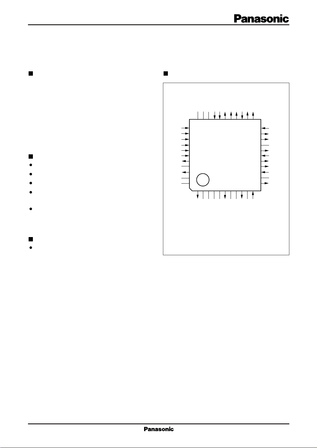
Pin Assignment Overview
The MN67621F generates color video camera synchronizing signals for the NTSC, PAL, and SECAM video
systems.
It divides the reference frequency to generate the horizontal synchronizing signal f
signal f
, and the composite synchronizing signal.
V
A built-in 4f
crystal oscillator circuit divides the fre-
SC
, the vertical synchronizing
H
quency by four to generate the color subcarrier frequency
signals SC1 and SC2.
Features
Supports CCDs with 420, 510, 590, and 670 H pixels
Supports NTSC, PAL, and SECAM video systems
PAL system 25Hz offset
Includes built-in oscillator circuit using external
crystal
Generates 14 signals, including the horizontal and
vertical synchronizing signals and the color
subcarrier frequency signals.
TEST1
TEST2
TEST3
V
SS1
CLK
V
DD1
EO
N.C.
ED
N.C.
N.C.
N.C.
N.C.
N.C.
CCDS2
CCDS1
CSYNC
CBLK
3332313029282726252423
34
35
36
37
38
39
40
41
42
43
44
1234567891011
VD
N.C.
N.C.
N.C.
N.C.
N.C.
PBLK
(TOP VIEW)
CP2
N.C.
TVMD2
SCBLK
WBKL
FMTP
22
21
20
19
18
17
16
15
14
13
12
OSCI
TVMD1
LSW
BFIDP
N.C.
WHD
V
SS2
SC2
SC1
V
DD2
N.C.
OSCO
Applications
Color video cameras
QFP044-P-1010
Page 2
MN67621F For Video Equipment
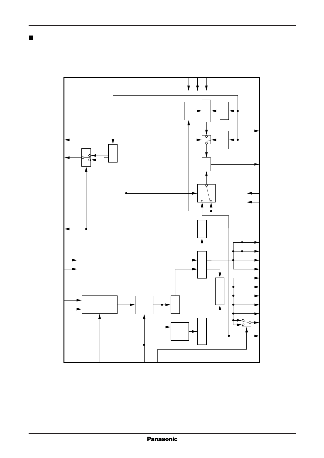
Block Diagram
TEST1
TEST2
TEST3
34
35
36
SC1
SC2
LSW
V
DD2
V
DD1
CCDS2
CCDS1
1/2
1/2
MIXER
SC
15
4f
(P)
(N)
1/910
16
1/4
øD
H/fV
f
(P)
(N)
12
OSCO
11
OSCI
40
EO
17
V
SS2
37
V
SS1
21
1/2
42
HD
18
14
39
30
29
1/3
1/8
1/5
202fH/206fH
1/7
2fH
1/101
1/103
fH
1/2
H dec.
C dec.
2fH
fV
1/525
1/625
V dec.
WHD
26
CP2
23
FMTP
9
WBLK
27
CBLK
28
CSYNC
24
SCBLK
6
PBLK
20
BFIDP
1
VD
38
CLK
22
TVMD1
25
TVMD2
Page 3
For Video Equipment MN67621F
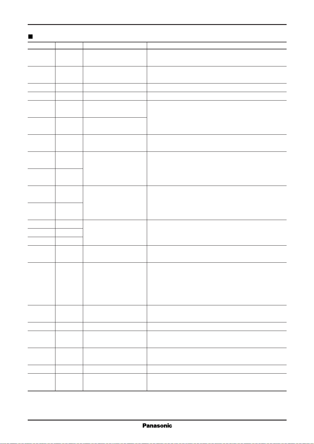
Pin Descriptions
Pin No. Symbol Pin Name Function Description
39 V
37 V
14 V
17 V
DD1
SS1
DD2
SS2
11 OSCI Crystal oscillation
12 OSCO Crystal oscillation
38 CLK Clock input
22 TVMD1
25 TVMD2
29 CCDS1
30 CCDS2
34 TEST1
35 TEST2 Test input
36 TEST3
15 SC1 f
16 SC2 fSC (R-Y) output
28 CSYNC Composite synchronizing
1 VD Vertical drive output
18 WHD Wide HD output
27 CBLK Composite blanking
42 HD Horizontal drive output
26 CP2 Clamp pulse output
Power supply "H" level (5 V) power supply for horizontal and vertical
synchronizing signal circuits
Power supply "L" level (0 V) power supply for horizontal and vertical
synchronizing signal circuits
Power supply "H" level (5 V) power supply for color subcarrier circuits
Power supply "L" level (0 V) power supply for color subcarrier circuits
Connect these pins to a 4fSC crystal oscillator.
input
The pins have built-in feedback resistors.
If using an external clock, supply it to the OSCI pin and
input
leave the OSCO pin open.
Supply the reference clock for the horizontal and vertical
synchronizing signals.
NTSC PAL SECAM
Television system
selection input
TVMD1 "H" "L" "L"
TVMD2 — "H" "L"
The pins include built-in pull-up resistors.
420H 510H 590H 670H
CCD scan lines
selection input
CCDS1 "H" "H" "L" "L"
CCDS2 "H" "L" "H" "L"
The pins include built-in pull-up resistors.
Test inputs Keep these pins at "L" level.
The pins include built-in pull-down resistors.
(B-Y) output
SC
This color subcarrier signal is formed by dividing the
crystal oscillator frequency (4f
) by four.
SC
Color subcarrier signal
If SC1 is the 180° signal, this signal has the following phase.
NTSC system: 90°
PAL system: 90° when LSW is at "L" level
270° when LSW is at "H" level
Composite blanking signal
signal output
Vertical drive signal
Wide HD signal
Preblanking signal
Composite blanking signal
output
Signal for erasing video signal
Horizontal drive signal
Clamp pulses for luminance and color difference signals
Horizontal deflection start pulses
Page 4
MN67621F For Video Equipment
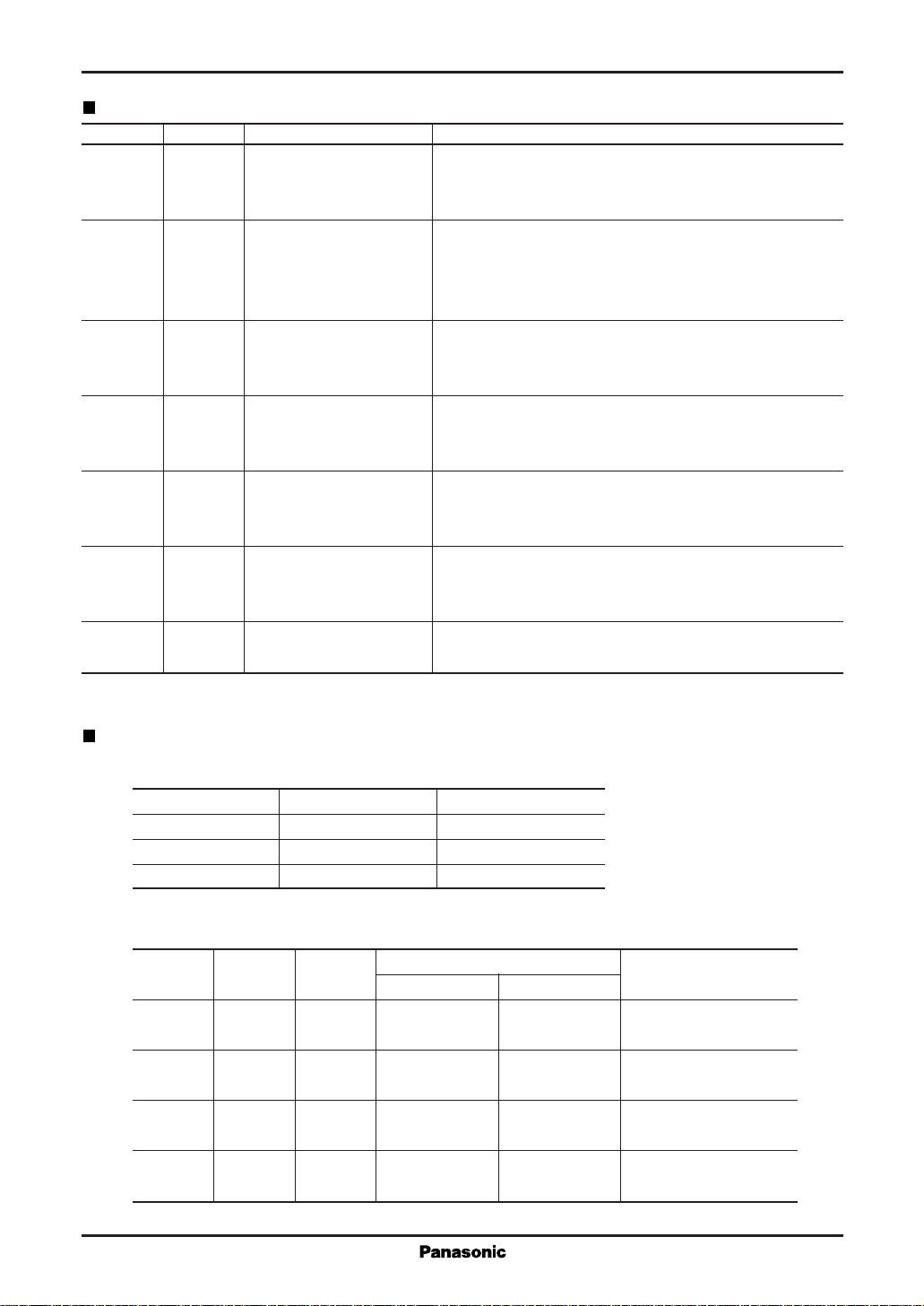
Pin Descriptions (continued)
Pin No. Symbol Pin Name Function Description
9 WBLK Composite wide blanking
output
20 BFIDP Output for burst flag/
identification signal
6 PBLK Composite preblanking
output
21 LSW Line switch signal
output
23 FMTP Trigger signal output
24 SCBLK Subcarrier blanking
signal output
40 EO Phase comparator
output
Composite wide blanking signal
This pin produces blanking pulses wider than the CELK
pulses for both horizontal and vertical synchronization.
For NTSC and PAL systems, this is the burst flag (BF)
output, which gates the color subcarrier signal.
For the SECAM system, this is the identification (IDP)
signal, which switches the subcarrier waveform.
Composite preblanking signal
This pin produces blanking pulses narrower than the CBLK
pulses for both horizontal and vertical synchronization.
Line switch signal
The chip generates this signal for each horizontal scan line.
During NTSC operation, this pin remains at "L" level.
This pin provides the FM demodulator trigger signal for the
SECAM system.
During NTSC operation, this pin remains at "L" level.
This pin provides the signal for erasing the subcarrier signal
for the SECAM system.
During NTSC operation, this pin remains at "L" level.
Phase comparator output
Operating Modes
(1) Television system
TVMD1 TVMD2
NTSC H —
PAL L H
SECAM L L
(2) CCD pixels and reference clock (CLK) frequencies
CCD CLK frequency (MHz) Frequency divider ratio
pixels
420H H H
510H H L
590H L H
670H L L
CCDS1 CCDS2
NTSC PAL/SECAM for first stage
15.891606 16.09375
(1010fH) (1030fH)
9.534964 9.65625
(606fH) (618fH)
22.248249 22.53125
(1414fH) (1442fH)
25.426570 25.75000
(1616fH) (1648fH)
1/5
1/3
1/7
1/8
Page 5

For Video Equipment MN67621F
H Decoder Pulse Timing Chart for NTSC
H-SYNC
CSYNC EO
V-SER
BF
CBLK
HD
WHD
CP2
PBLK
WBLK
–9.12
–4.72
–1.57
(
*
2.20
1
)
4.720
5.35 7.87
7.24
8.50
9.44
1H=63.55µs
Unit: µs
17.52
1
*
420 H : 2.33
510 H : 2.31
590 H : 2.34
670 H : 2.36
Page 6

MN67621F For Video Equipment
Pulse Timing Chart for NTSC Composite and Vertical Synchronizing Signals (1/2)
52452512345678910111213141516171819202122
CSYNC
BF
CBLK
VD
PBLK
9H
261 262 263 264 265 266 267 268 269 270 271 272 273 274 275 276 277 278 279 280 281 282 283 284 285
21.0H + 11.0µs
16H + 8.8µs
CSYNC
BF
CBLK
VD
PBLK
9H
21.0H
16H
Pulse Timing Chart for NTSC Composite and Vertical Synchronizing Signals (2/2)
CSYNC
WBLK
CSYNC
WBLK
488489490 52512345678910 99100101102
135.5H + 7.5µs
226 227 262 263 264 265 266 267 268 269 270 271 272 361 362 363 364
135.5H + 19.2µs
Page 7

For Video Equipment MN67621F
H Decoder Pulse Timing Chart for PAL/SECAM
H-SYNC
CSYNC EO
V-SER
BF
CBLK
HD
WHD
CP2
PBLK
WBLK
0 4.66
1
(
)
*
–4.66
5.59 7.77
8.38
2.17
–6.70 17.40
1H=64µs
10.56–1.55
Unit: µs
IDP
SCBLK
FMTP
– 0.31
5.29
13.0
1
*
420 H : 2.30
510 H : 2.28
590 H : 2.31
670 H : 2.33
Page 8

MN67621F For Video Equipment
Pulse Timing Chart for PAL/SECAM Composite and Vertical Synchronizing Signals (1/2)
620621622623624625123456789101112131415161718192021222324252627
CSYNC
)
BF-(1
)
BF-(3
CBLK
VD
PBLK
IDP
SCBLK
LSW(1
LSW(3
7.5H
)
)
25H
21H + 8.8µs
CSYNC
)
BF-(2
)
BF-(4
CBLK
VD
PBLK
IDP
SCBLK
LSW(2
LSW(4
308 309 310 311 312 313 314 315 316 317 318 319 320 321 322 323 324 325 326 327 328 329 330 331 332 333 334 335 336 337 338 339
25H + 12.1µs
7.5H
21H
)
)
Page 9

For Video Equipment MN67621F
Pulse Timing Chart for PAL/SECAM Composite and Vertical Synchronizing Signals (2/2)
584 586
585 622623624625123456 979899100
CSYNC
WBLK
CSYNC
WBLK
137.5H + 7.2µs
272 273 274 310 311 312 313 314 315 316 317 318 409 410 411 412 413
137.5H + 19.0µs
Page 10

MN67621F For Video Equipment
Application Circuit Example
3332313029282726252423
N.C
N.C
5V
34
35
36
37
38
39
40
41
42
43
44
TEST1
TEST2
TEST3
V
SS1
CLK
V
DD1
EO
N.C
HD
N.C
N.C
N.C
CCDS1
CCDS2
MN67621F
CBLK
CSYNC
CP2
SCBLK
TVMD2
TVMD1
BFIDP
OSCO
FMTP
LSW
N.C
WHD
V
SS2
SC2
SC1
V
DD2
N.C
22
21
20
19
18
17
16
15
14
13
12
Reference clock input
VD
N.C
N.C
N.C
N.C
N.C
N.C
PBLK
1234567891011
N.C
WBLK
OSCI
Page 11

For Video Equipment MN67621F
Package Dimensions (Unit: mm)
QFP044-P-1010
12.30±0.40
10.00±0.20
34
44
(1.00)
33
23
22
(1.00)
10.00±0.20
12.30±0.40
12
111
0.80
0.35±0.10
2.00±0.20
2.10±0.30
+0.10
1.15±0.20
0.05
-
0.15
0 to 10°
0.10
SEATING PLANE
0.10±0.10
0.60
±0.20
 Loading...