

Page 1
Ordering number: EN5204A
Monolithic Linear IC
LA4587M
Preamplifier + Power Amplifier
for 1.5 V Headphone Stereos
Overview
The LA4587M is a system IC that includes all of the necessary
functions for a playback set on a single chip, reducing the
number of external components needed.
Functions
.
Stereo preamplifier (supports auto reverse function,
switchable between metal and normal tape)
.
Stereo power amplifier (OCL, mute function)
.
Ripple filter
.
Low boost function (BTL operation in low-frequency range)
.
AMSS (Automatic Music Select System)
.
Power switch
Features
.
Preamplifier has a high open-loop gain (VGO= 73 dB).
.
Preamplifier requires no NF capacitor.
.
Virtual ground capacitor can be 1 µF or less. (Lower
impedance is achieved by having a V
.
Ripple filter requires no capacitor for preventing oscillation.
.
Powerful output is obtained in low boost output
(Po = 21 mW/V
.
A high-frequency cutoff capacitor is built into the
preamplifier and power amplifier inputs; anti-buzz provision.
= 1.2 V, f = 100 Hz).
CC
amplifier built in.)
REF
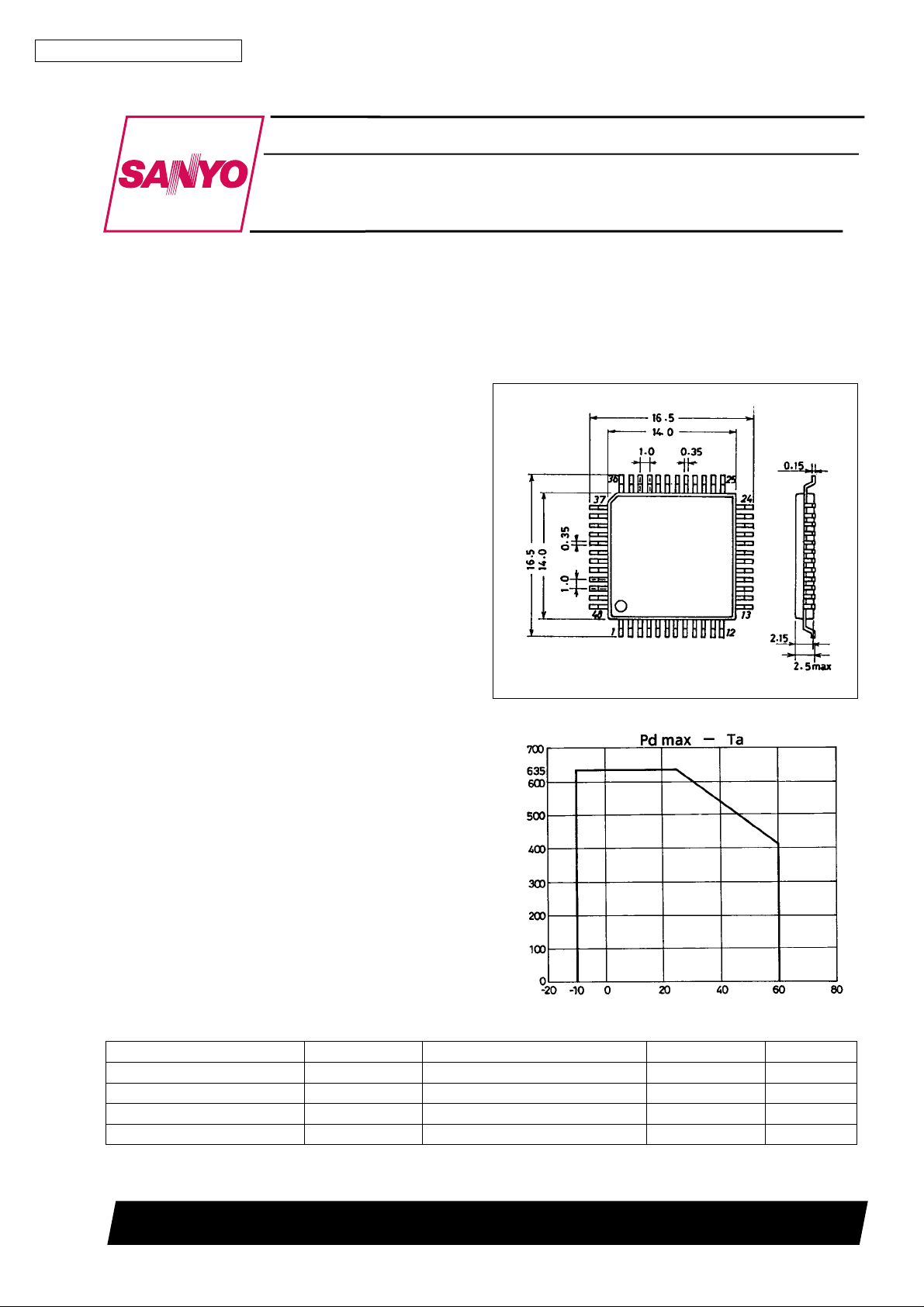
Package Dimensions
unit : mm
3102-QFP48D
[LA4587M]
SANYO : QIP48D
Specifications
Maximum Ratings atTa=25°C
Parameter Symbol Conditions Ratings Unit
Maximum supply voltage V
Allowable power dissipation Pd max 635 mW
Operating temperature Topr –10 to +60
Storage temperature Tstg –40 to +125
max 3.0 V
CC
Allowable power dissipation, Pd max − mW
Ambient temperature, Ta −°C
SANYO Electric Co.,Ltd. Semiconductor Bussiness Headquarters
TOKYO OFFICE Tokyo Bldg., 1-10, 1 Chome, Ueno, Taito-ku, TOKYO, 110 JAPAN
13097HA(II)/N3095HA(II) No.5204-1/18
C
°
C
°
Page 2
LA4587M
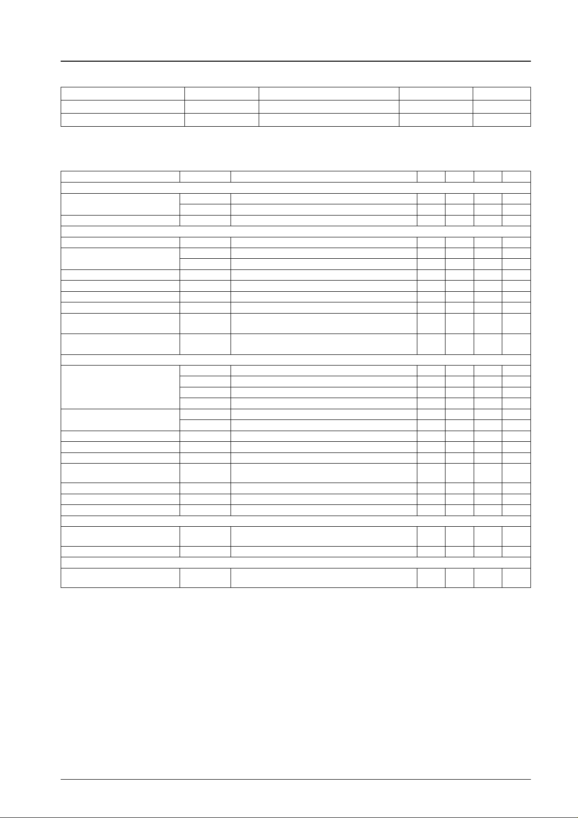
Operating Conditions atTa=25°C
Parameter Symbol Conditions Ratings Unit
Recommended supply voltage V
Operating supply voltage range V
CC
op 0.95 to 2.2 V
CC
Operation Characteristics atTa=25°C, VCC=1.2V,f=1kHz, 0.775 V = 0 dBm,
=10kΩ(preamplifier), RL=16Ω(power amplifier)
R
L
Parameter Symbol Conditions min typ max Unit
[Preamplifier + Power Amplifier]
I
1 Rg = 2.2 kΩ,Rv=0Ω 81524mA
Quiescent current
Voltage gain (closed) VG
[Preamplifier]
Voltage gain (open) VG
Voltage gain (closed)
Maximum output voltage V
Total harmonic distortion THD
Equivalent input noise voltage V
Interchannel crosstalk CT
Interchannel crosstalk between
F and R
Ripple rejection ratio Rr1
[Low Boost + Power Amplifier]
Voltage gain (closed)
Output power
Total harmonic distortion THD
Interchannel crosstalk CT
Output noise voltage V
Ripple rejection ratio Rr
Output mute voltage V
Input resistance Ri 8 10 12 kΩ
Voltage gain difference ∆VG
[Ripple Filter ]
Ripple rejection ratio Rr
Output voltage V
[AMSS]
Operating output voltage V
CCO
I
2 When power switch is off 0.1 5 µA
CCO
VG
VG
max THD=1% 100 210 mV
O
NI
CT
VO= –20 dBm, RV=10kΩ 54 57 60 dB
T
VO= –20 dBm 60 73 dB
0
VO= –20 dBm 34 35.5 37 dB
1
VO= –20 dBm, f = 10 kHz, metal on 25.5 28 30.5 dB
2
VG = 35.5 dB/NAB, VO= 100 mV 0.1 0.5 %
1
Rg = 2.2 kΩ, BPF: 20 Hz to 20 kHz 1.3 3.0 µV
Rg = 2.2 kΩ, 1 kHz TUNE, VO= –20 dBm 45 56 dB
1
Rg = 2.2 kΩ, 1 kHz TUNE, VO= –20 dBm 65 78 dB
2
Rg = 2.2 kΩ, Vr = –30 dBm,
fr = 100 Hz, 100 Hz TUNE
VG
VG
VG
VG
P
O1
P
O2
NO
M
RF
OAMSS
VO= –20 dBm 20.5 23 25.5 dB
3
VO= –20 dBm, L.B. = on 20.5 23 25.5 dB
4
VO= –20 dBm, L.B. = on,f=10kHz 24.5 27.5 30.5 dB
5
VO= –20 dBm, L.B. = on, f = 100 Hz 30 34 38 dB
6
THD=10% 5 9 mW
THD = 10 %, f = 100 Hz, L.B. = on 13 21 mW
PO= 1 mW 0.5 1.5 %
2
VO= –20 dBm, RV=0Ω 38 43 dB
3
RV=0Ω, BPF: 20 Hz to 20 kHz 35 48 µV
RV=0Ω, Vr = –30 dBm,
2
fr = 100 Hz, 100 Hz TUNE
VIN= –30 dBm, 1 KHz TUNE, mute on –85 dBm
3
fr = 100 Hz, Vr = –30 dBm, VCC= 1.0 V,
3
I
= 25 mA, 2SB1295, hFE6 rank used
RF
VCC= 1.0 V, IRF= 25 mA 0.89 0.93 V
Preout voltage when AMSS VO= 0.6 Vp-p
Pin 34 is short-circuited through 270 kΩ.
1.5 V
45 52 dB
50 74 dB
0 +1.5 dB
33 39 dB
1.80 2.55 3.60 mV
Note: L.B. = Low boost
No.5204-2/18
Page 3
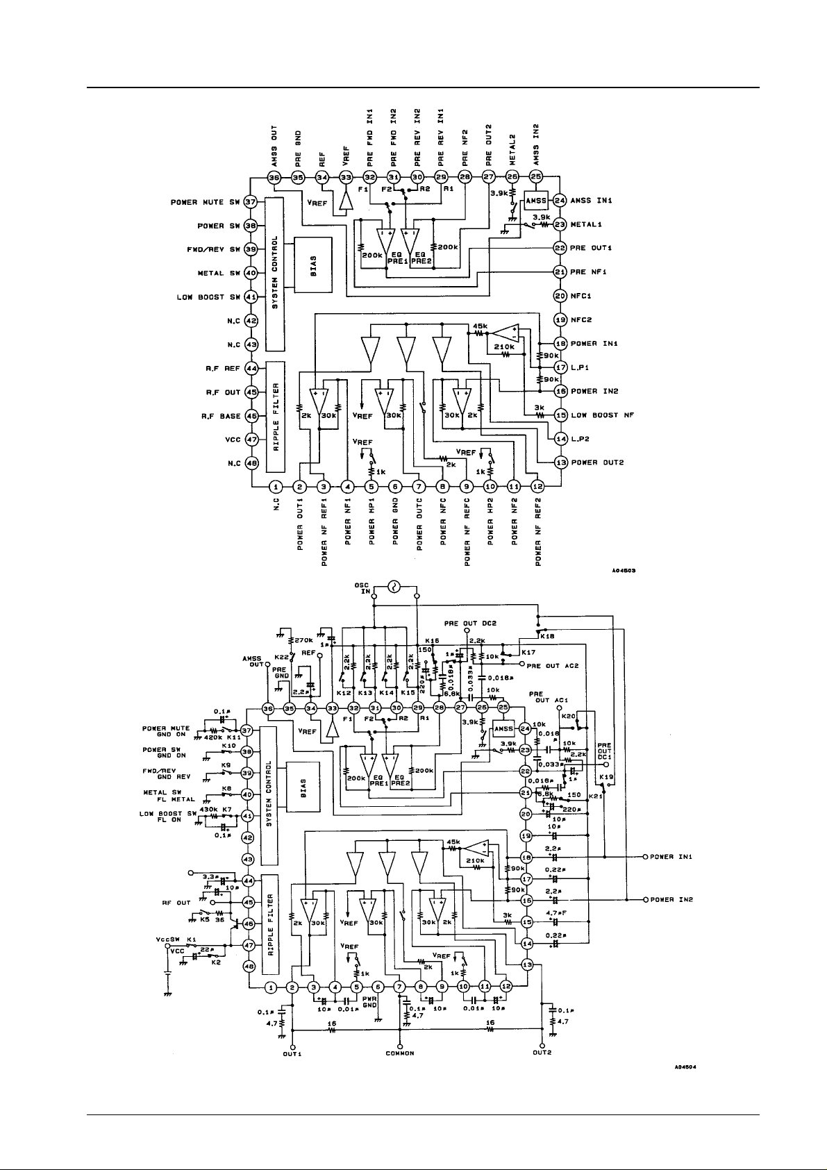
Block Diagram
LA4587M
Test Circuit Diagram
Unit (resistance: Ω)
Unit (resistance: Ω, capacitance: F)
No.5204-3/18
Page 4

Sample Application Circuit
LA4587M
Unit (resistance: Ω, capacitance: F)
Note 1: Transistors equivalent to the 2SB1295 with hFE6 rank and upward are recommended.
Note 2: C18, C23, and C26 are oscillation prevention capacitors; a polyester film or ceramic capacitor (which can guarantee the
specified capacitance at operating temperatures) is recommended.
No.5204-4/18
Page 5
Pin Functions
Pin No. Pin name
45 R.F OUT 1.13
2
POWER OUT1
7
POWER OUTC
13
POWER OUT2
3
POWER NF REF1
9
POWER NF REFC
LA4587M
Unit (resistance:Ω, capacitance: F) * Pin voltage is when VCC= 1.2 V
Pin voltage
[V]
0.6 c A 160 Ω resistor is connected
0.75
Internal equivalent circuit Remarks
between individual outputs
(between pins 2 and 7, and
between pins 13 and 7).
c Each power NF connection
12
POWER NF REF2
4
POWER NF1
8
POWER NFC
11
POWER NF2
510POWER H.P1
POWER H.P2
14 L.P2 0.75
0.75
0.75
c Each power NF connection.
c Grounded to V
1kΩresistor when low boost
is on (pin 41: floating).
c Low boost secondary LP
connection.
REF
through a
Continued on next page.
No.5204-5/18
Page 6

LA4587M
Continued from preceding page. Unit (resistance: Ω, capacitance: F)
Pin No. Pin name
15 Low Boost NF 0.75
Pin voltage
[V]
Internal equivalent circuit Remarks
c Low boost amplifier NF
connection.
1618POWER IN2
POWER IN1
17 L.P1 0.75
1920NFC2
NFC1
2128PRE NF1
PRE NF2
0.75
0.75
0.75 c Each preamplifier NF
c Each power input connection.
c The input resistance is
10 kΩ.
c An anti-buzz capacitor is built
in.
c Low boost primary LP.
connection.
connection.
c NF requires no capacitor.
2227PRE OUT1
PRE OUT2
0.45
c 200 kΩ is connected
between each output pin and
NF pin.
Continued on next page.
No.5204-6/18
Page 7

LA4587M
Continued from preceding page. Unit (resistance: Ω, capacitance: F)
Pin No. Pin name
2326METAL1
METAL2
Pin voltage
[V]
0
Internal equivalent circuit Remarks
c Connected to GND through
3.9 kΩ in metal on mode (pin
40: floating)
2425AMSS IN1
AMSS IN2
29
PRE REV IN1
30
PRE REV IN2
31
PRE FWD IN2
32
PRE FWD IN1
33 V
REF
34 REF 0.75
0.75
0.75
0.75 c V
c AMSS inverting input
connection.
c An external input resistor is
required.
b Pins 29 and 30 turn on in
REV mode (pin 39: GND).
c Pins 31 and 32 turn on in
FWD mode (pin 39: floating)
c When not using the head, a
bias resistor (2.2 kΩ)is
required between these pins
and V
c An anti-buzz capacitor is built
in.
REF
impedance is achieved due
to the output resistor (ro =
10 Ω).
c Inflow/outflow current:
200 µA max.
c The V
referenced hereto.
(pin 33).
REF
amplifier output. Low
amplifier is
REF
36 AMSS OUT
c Outputs a pulse waveform in
accordance with the AMSS
IN (pins 24 and 25) input
level.
Continued on next page.
No.5204-7/18
Page 8

LA4587M
Continued from preceding page. Unit (resistance: Ω, capacitance: F)
Pin No. Pin name
3741POWER MUTE SW
Low Boost SW
Pin voltage
[V]
Internal equivalent circuit Remarks
c When pin 37 is grounded,
mute is on.
c When pin 41 is floating, low
boost is on.
38 POWER SW
3940FWD/REV SW
METAL SW
44 R.F REF 1.13
46 R.F BASE 0.5
c Power on when grounded.
c When pin 39 is floating: FWD
mode; when grounded: REV
mode.
c When pin 40 is in FL mode:
metal on.
c RF is referenced hereto. An
external capacitor can be
used to vary RF SVRR.
c Used for external PNP
transistor base drive.
No.5204-8/18
Page 9

LA4587M
Description of External Components
.
C1(1.0 to 10 µF): V
.
C2,C10: Playback preamplifier EQ constant.
.
C3,C9(0.47 to 3.3 µF): Preamplifier output capacitor.
.
C4,C8: AMSS input HPF capacitor.
.
C5,C7: EQ constant for metal (built-in resistance 3.9 kΩ±15%).
.
C6(0.1 to 22 µF): V
.
C11,C12(3.3 to 10 µF): NFC decoupling capacitor.
.
C13,C15(1.0 to 3.3 µF): Power amplifier input capacitor (Input resistance: 10 kΩ).
.
C14,C17: Capacitor for low boost LPF.
.
C16(1.0 to 4.7 µF): Boost amplifier NF capacitator.
.
C18,C23,C26(0.1 to 1.0 µF): Oscillation blocking capacitator.
.
C19,C22,C25(3.3 to 10 µF): Power amplifier NF capacitor.
.
C20,C24: Bass high boost capacitor.
.
C21(100 to 2200 pF): Oscillation blocking capacitator.
.
C29(4.7 to 10 µF): RF output decoupling capacitor. (Also serves as the power supply capacitor and the
.
C28(22 to 220 µF): Power supply capacitor.
.
C30(2.2 to 10 µF): RF is referenced to this LPF capacitor.
.
C31,C32(0.047 to 0.22 µF): Switching circuit smoothing capacitor. Must be adjusted according to the set timing.
.
R1,R10: For preamplifier gain adjustment.
.
R2,R9: Playback preamplifier EQ constant.
.
R3,R8: EQ constant for metal.
.
R4,R7:10kΩvolume control.
.
R5,R6: For AMSS gain adjustment and HPF.
.
R11,R12,R13: For oscillation blocking.
.
R14,R15(100 to 430 kΩ): For switching circuit smoothing (discharge resistors).
amplifier is referenced to this decoupling capacitor.
REF
The V
Note that if the capacitance is reduced, the SVRR worsens.
REF
For high-frequency noise rejection.
Note that if the capacitance is reduced, the preamplifier low-frequency gain decreases.
The low boost gain depends on the capacitance.
Note that if the capacitance is reduced, the low boost low-frequency gain decreases.
Note that if the capacitance is reduced, the power amplifier low-frequency gain decreases.
The high gain depends on the capacitance.
oscillation blocking capacitor.)
The RF SVRR depends on the capacitance.
SVRR depends on the value of this capacitor.
REF
decoupling capacitor.
No.5204-9/18
Page 10

Operation Descprition
.
Low boost system
Low-frequency region amplification: 12 dB/oct, high-frequency region amplification: 6 dB/oct.
LA4587M
Phase 90
.
Note on low boost
The signals that are applied to each power input are mixed and then passed through a two-stage LPF. Because the signal levels
are attenuated by the LPF, level compensation is accomplished by amplifying the signals through a low boost amplifier located
in between. The phase of signals that pass through the secondary LPF is inverted relative to the input signal; these signals are
then input to each power amplifier.
.
Note on channels 1 and 2
The positive phase signals that were input from the positive (‘‘+’’) input pins and the reverse phase signals that were input from
the negative (‘‘–’’) input pins and then were passed through the secondary LPF are all input, amplified, and then output.
.
Note on the common amplifier
The phase of the signals that passed through the secondary LPF is inverted by the inverting amplifier; the signals (with reversed
phases relative to channels 1 and 2) are then input to the negative (‘‘–’’) inputs. The positive (‘‘+’’) input signals are grounded
to V
, amplified by the inverting amplifier and then output.
REF
The phase of the channel 1 and 2 amplifier outputs and the common amplifier outputs are made to oscillate with inverted
phases, making it possible to obtain the dynamic range efficiently.
°
Phase 180
°
No.5204-10/18
Page 11

LA4587M
Sample Application Circuits for Low Boost Switching
Sample 1
Sample 2
In the above circuits, MID and MAX are switched by changing the gain of the boost amplifier.
The AMSS comparator
Block Diagram
No.5204-11/18
Page 12

LA4587M
Operation Description
.
The input amplifiers are inverting amplifiers. The gain and HPF characteristics can be adjusted through an external C-R
(input impedance).
.
The AMSS comparator outputs pulses for an input waveform that satisfies certain set conditions (frequency and voltage
level).
Input
Output
.
When AMSS is not used, the input pins (pins 24 and 25) are connected to V
REF
(pin 33).
Notes on the ripple filter
.
The RF SVRR can be adjusted by an external capacitor connected to pin 44.
3.3 µF → 39 dB
4.7 µF → 42 dB
10 µF → 47 dB
.
It is recommended that external transistors be equivalent to the 2SB1295 with hFE6 rank and upward.
Note on power output
.
The power amplifier output and the common amplifier output are connected by a resistor of approximately 160 Ω.
Notes on power mute
.
Power mute turns off the fixed current that is supplied to the power section.
.
The output DC when power mute is on is the V
.
The output impedance when power mute is on is approximately 10 kΩ.
electric potential (0.75 V).
REF
No.5204-12/18
Page 13

SW Pin Equivalent Circuit Diagram
1. Power switch
LA4587M
On when power switch is grounded
I
O=VCC
Pin 38
V
/200k+VCC– 0.7 V/22 kΩ
= 100 mV or less
S
2. Power mute and low boost switch
3. FWD/REV, METAL switch
On when pin 37 power mute is grounded
On in pin 41 low boost switch floating mode
I
= 0.1 µA or less
O
V
= 80 mV or less
S
* The discharge resistance for
smoothing is 430 kΩ max.
REV when pin 39 FWD/REV is grounded
On in pin 40 metal floating mode
I
= 7 µA or less
O
V
= 0.5 V or less
S
No.5204-13/18
Page 14

LA4587M
—mA
CCO
Quiescent current, I
—dB
o
On
On
Supply voltage, VCC—V
Preamplifier
VG, VG
O–VCC
—dB
o
Open loop gain, VG
Closed loop gain, VG — dB
Preamplifier
Preamplifier
VG,VGO–f
i
DIN AUDIO used
Frequency, fi—Hz
THD–V
O
to
Normal
Metal
Open-loop gain, VG
Crosstalk, CT — dB
Closed-loop gain, VG — dB
Total harmonic distortion, THD — %
Supply voltage, VCC—V
Interchannel CT − f
i
Preamplifier
C
VREF
Frequency, fi—Hz
Crosstalk, CT — dB
used
Supply voltage, VO—mV
CT−f
between FWD/REV
i
Preamplifier
Frequency, fi—Hz
used
Between FWD/REV
—µV
Interchannel CT
NO
Preamplifier
Preamplifier
Crosstalk, CT — dB
Supply voltage, VCC—V
Output noise voltage, V
Supply voltage, VCC—V
to
No.5204-14/18
Page 15

V
REF
V
REF
LA4587M
V
REF
—%
—%
REF
ODC
V
V
— dBm
OUT
Output, V
Supply voltage, V
V
OUT—fi
Frequency, f
CC
—Hz
i
—V
C
VREF
Preamplifier
Ripple rejection ratio, SVRR — dB
— dBm
OUT
Output, V
V
C
V
REF
VREF
REF
Pre+V
Supply voltage, V
V
—V
OUT
Supply voltage, V
V
—IV
REF
FWD/REV
equivalent
—V
CC
CC
—V
CC
REF
REF
ro — Ω
V
C
Pre out. = 6 mV
Input H.P.
AMSS — mV
o
Operating output voltage, V
REF
VREF
Supply voltage, V
V
O
Input on both channels
Input on one channel
Pre-output — Hz
CC
—V
—V
REF
V
Pre out. = 6 mV
AMSS — mV
o
Operating output voltage, V
IV
—µA
V
Input on both channels
Supply voltage, V
REF
O
Input on one channel
CC
—V
No.5204-15/18
V
REF
Page 16

LA4587M
Input on both channels
AMSS — mV
o
Input on one channel
—V
RFO
Input H.P
Output ripple voltage, V
Operating output voltage, V
Pre-output — mV
Supply voltage, V
CC
—V
—V
RFO
Ripple rejection ratio, SVRR — dB
Output ripple voltage, V
Ripple rejection ratio, SVRR — dB
—V
RFO
Output ripple voltage, V
Supply voltage, V
Output ripple current, I
CC
I
RFO
RFO
—V
—mA
Supply voltage, V
CC
I
RFO
—V
—V
RFO
Output ripple voltage, V
Ripple rejection ratio, SVRR — dB
Output ripple current, I
V
,
RFO
RFO
—mA
Ripple rejection ratio, SVRR — dB
—V
RFO
Ripple rejection ratio, SVRR — dB
Frequency, f
—Hz
R
Output ripple voltage, V
Ripple voltage, V
—mV
R
Ripple rejection ratio, SVRR — dB
No.5204-16/18
Page 17

When low boost is on
When low boost is off
f
i
LA4587M
Output on both
channels
on
on
on
off
Voltage gain, VG — dB
Input on both channels
max—V
O
Output voltage, V
max—V
O
Frequency, fi—Hz
V
O
on
Supply voltage, VCC—V
V
max—f
O
i
L.B.= on
Input on both channels,
Load on both channels
L.B. + Power
Voltage gain, VG — dB
Input on both
channels
—mW
O
Output power, P
—mW
O
Output on both channels
Supply voltage, VCC—V
P
O
on
Supply voltage, VCC—V
PO—f
i
V
O
L.B. = on
Input on both chanels,
Load on both channels
Output voltage, V
—V
ODC
V
Frequency, fi—Hz
Supply voltage, VCC—V
Output power, P
Frequency, fi—Hz
THD—f
i
on
off
Input on both
channels
Total harmonic distortion, THD — %
No filter
Frequency, fi—Hz
No.5204-17/18
Page 18

LA4587M
f
i
on
off
—µV
NO
on
off
Crosstalk, CT — dB
Output noise voltage, V
Frequency, fi—Hz
Supply voltage, VCC—V
off
on
Ripple rejection ratio, SVRR — dB
Supply voltage, VCC—V
No products described or contained herein are intended for use in surgical implants, life-support systems, aerospace equipment,
nuclear power control systems, vehicles, disaster/crime-prevention equipment and the like, the failure of which may directly or
indirectly cause injury, death or property loss.
Anyone purchasing any products described or contained herein for an above-mentioned use shall:
1 Accept full responsibility and indemnify and defend SANYO ELECTRIC CO., LTD., its affiliates, subsidiaries and distributors
and all their officers and employees, jointly and severally, against any and all claims and litigation and all damages, cost and
expenses associated with such use:
2 Not impose any responsibility for any fault or negligence which may be cited in any such claim or litigation on SANYO
ELECTRIC CO., LTD., its affiliates, subsidiaries and distributors or any of their officers and employees jointly or severally.
Information (including circuit diagrams and circuit parameters) herein is for example only; it is not guaranteed for volume
production. SANYO believes information herein is accurate and reliable, but no guarantees are made or implied regarding its use
or any infringements of intellectual property rights or other rights of third parties.
This catalog provides information as of January 1997. Specifications and information herein are subject to change without notice.
No.5204-18/18
 Loading...