

Page 1
Any and all SANYO products described or contained herein do not have specifications that can handle
applications that require extremely high levels of reliability, such as life-support systems, aircraft’s
control systems, or other applications whose failure can be reasonably expected to result in serious
physical and/or material damage. Consult with your SANYO representative nearest you before using
any SANYO products described or contained herein in such applications.
SANYO assumes no responsibility for equipment failures that result from using products at values that
exceed, even momentarily, rated values (such as maximum ratings, operating condition ranges,or other
parameters) listed in products specifications of any and all SANYO products described or contained
herein.
Monolithic Linear IC
5.8W typ AF Power Amplifier for
Car Stereos, Car Radios
Ordering number:ENN556F
LA4422
SANYO Electric Co.,Ltd. Semiconductor Company
TOKYO OFFICE Tokyo Bldg., 1-10, 1 Chome, Ueno, Taito-ku, TOKYO, 110-8534 JAPAN
Features
• High gain (53dB typ.) and high output (5.8W typ).
• Soft clip.
• Small number of external parts (4 pcs).
• Bridge construction usable (PO=18W/RL=4Ω).
• Built-in thermal shutdown circuit against load short, over load.
• Built-in circuit to prevent pop noise at the time of power
supply ON.
• SIP package (single ended pins) facilitating easy mounting.
Specifications
Absolute Maximum Ratings at Ta = 25˚C
* : 100×100×1.5mm3 Al heat sink used.
Operating Conditions at Ta = 25˚C
Operating Characteristics at Ta = 25˚C, VCC=13.2V, RL=4Ω, f=1kHz, 100×100×1.5mm3 Al heat sink.
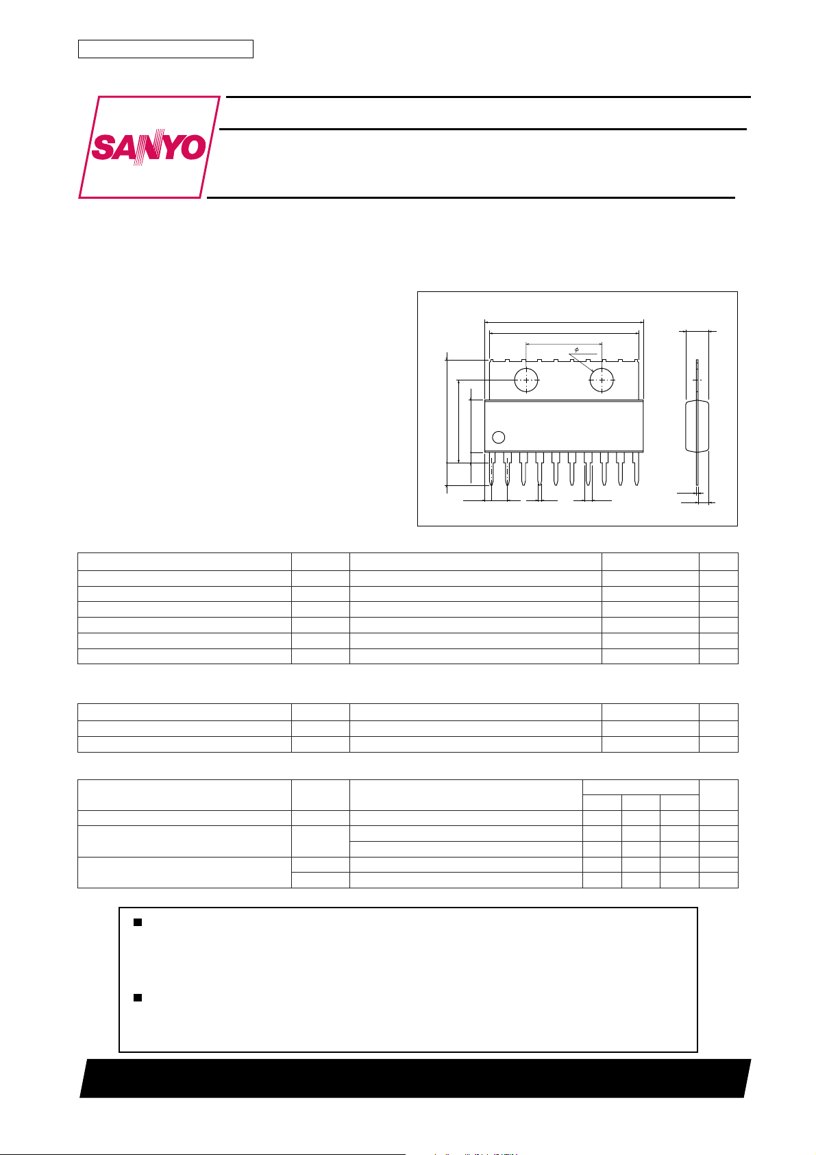
Package Dimensions
unit:mm
3018A-SIP10FD
[LA4422]
25.5
24.0
12.0
3.6
16.7max
13.5
8.4
3.5
1.6min
1.32
retemaraPlobmySsnoitidnoCsgnitaRtinU
egatlovylppusmumixaMV
tnerructuptuomumixaMIO*tuo-wolf01niP,tuo-wolf8nip,ni-wolf1niP 5.4A
egatlovylppusegruSegrusVt≤ s2.0 04V
noitapissidrewopelbawollAxamdP 7W
erutarepmetgnitarepOrpoT 57+ot02–
erutarepmetegarotSgtsT 051+ot04–
retemaraPlobmySsnoitidnoCsgnitaRtinU
egatlovylppusdednemmoceRV
ecnatsiserdaoldednemmoceRR
retemaraPlobmySsnoitidnoC
tnerructnecseiuQI
niagegatloVGV
rewoptuptuO
xam 81V
CC
CC
L
OCC
PO1R,%01=DHT
PO2R,%01=DHT
pooldesolC153555Bd
4= Ω 0.58.5W
L
2= Ω 0.9W
L
0.5
2.54
tiucricdeificepsnodesabpoolnepO07Bd
1.3
101
SANYO : SIP10FD
sgnitaR
nimpytxam
5308Am
Continued on next page
3.6
0.45
1.6
˚C
˚C
2.31V
Ω
4
tinU
21500TH (KT)/O281TS/D177KI/5085MW/6250KI, TS No.556–1/10
Page 2
Continued from preceding page.
retemaraPlobmySsnoitidnoC
noitrotsidcinomrahlatoTDHTPOW1=7.00.2%
ecnatsisertupnIir 03kΩ
egatlovesiontuptuOV
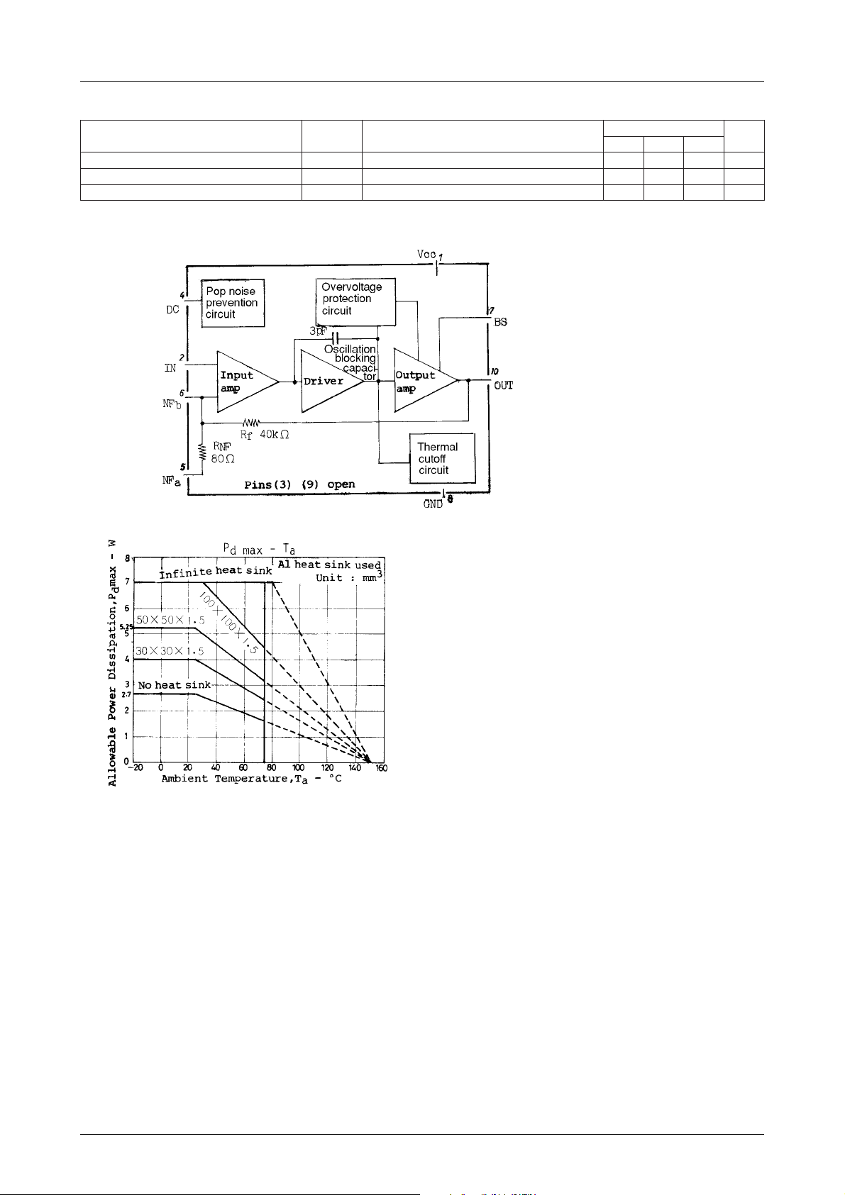
Equivalent Circuit Block Diagram
LA4422
sgnitaR
nimpytxam
ON
k01=gR Ω retlifon,2.15.2Vm
tinU
Proper Cares in Using IC
1. Maximum ratings
Extreme caution should be excrcised when using the IC in the vicinity of the maximum ratings as a slight factor may
cause the maximum ratings to be exceeded, thereby leading to a breakdown accident.
2. Pin-to-pin short
If the power supply is truned ON with pin-to-pin short, a breakdown or de-gradation may occur. When installing the IC
on the board, be sure to check that pin-to-pin area is not shorted with solder, etc. and turn ON the power supply.
3. Printed Circuit Board
When designing the printed circuit board, make the power supply and ground lines thicker and shorter so that no
feedback loop of input/output is formed. When using under the condition where the signal source impedance (Rg) is
large, a stable operation against distortion is obtained by separating the input /output ground line at the root of GND pin
[pin (8)]. The heat sink fin must be reliably connected to the external line of the same potential as pin (8) (GND).
No.556–2/10
Page 3
LA4422
Functions of External Parts
The recommended number of external parts of the LA4422 is 4 pcs. as follows.
· Feedback capacitor from pin (5) CNF.
· Pin (7) to (10) bootstrap capacitor CBS.
· Output capacitor from pin (10) C
· High frequency parasitic oscillation compensating capacitor CX.
The fixed values of these parts are CNF=100µF, CBS=100µF, C
when these values are changed.
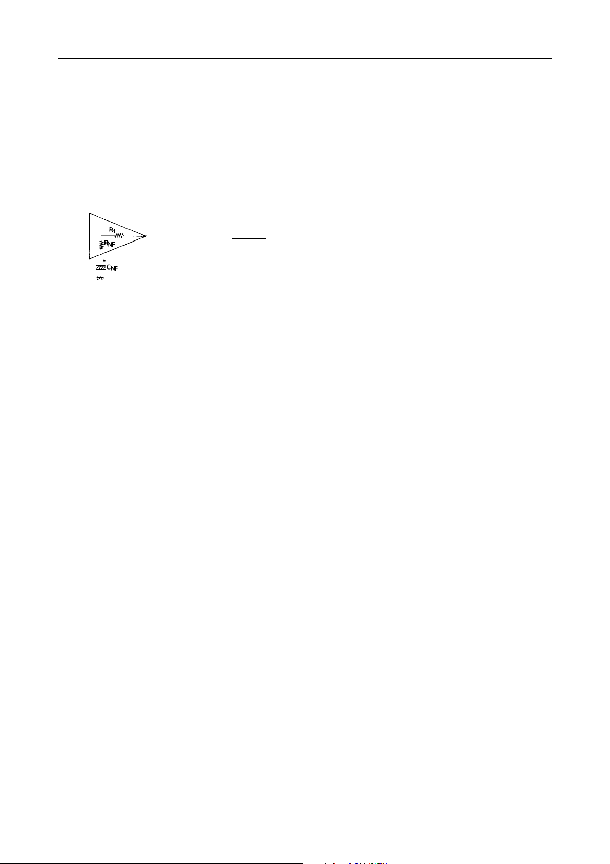
(a) Feedback capacitor C
NF
If CNF is made smaller, the combined series impedance with RNF at a low frequency is increased, the amplification
degree Avf is decreased, and the low cutoff frequency is made higher as seen from the following equation.
Avf=
VG=20log A vf (dB)
The ripple rejection is also lowered. It is possible, however, to make the starting time earlier at the time of the power
supply switch ON. If CNF is made larger, these are reversed.
.
OUT
Rf
(RNF+ )
jωC
1
NF
=1000µF, CX=0.15µF . We no w consider what will occur
OUT
(b) Bootstrap capacitor C
BS
The low cutoff frequency may be somewhat influenced, but the drive at a low frequency is more influenced. If CBS is
made smaller, power at a low frequency may be reduced. Therefore, CBS should be more than 47µF.
(c) Output capacitor C
OUT
The low cutoff frequency may be somewhat influenced, but the most influence is that power is reduced as the impedance at a low frequency is increased. Therefore, C
should be determined by the power band width. 470µF min. is
OUT
required.
(d) High frequency parasitic oscillation compensating capacitor CX.
CX should be a polyester film capacitor of good frequency characteristic. If a ceramic capacitor is used, oscillation may
occur.
Features of IC System and Functions of Remaining Pins
· Since the input circuit uses pnp and the input potential is designed to be 0 bias, no input coupling capacitor is needed and
the direct coupling is available.
· The thermal shutdouwn protection circuit is built in to prevent breakdown or degradation attributable to generation of heat
at the time of load short or overload.
· The overvoltage protection circuit is built in to protect the IC from breaking down when a surge is applied to the power
supply line.
· The prevention circuit is provided to prevent pop noise which occures when the power supply is turned ON.
· The voltage gain of open loop is lo wered and the nagative feedback is made smaller to obtain a soft clip. Radiation to the
high frequency circuit and stability are considered.
· The feedback resistor Rf is set up at such a large value as 40kΩ and the cutof f frequency point fL is considered so that the
frequency characteristic is fully externded to a low frequency even if the capacity of capacitor CNF is small.
· The high frequency parasitic oscillation compensating capacitor is built in as a means to reduce the number of external
parts. Therefore, the high cutoff frequency point fH is fixed.
· The feedback resistor RNF is built in and the voltage gain is fixed to be 53dB in order to reduce the number of external
parts and to minimize the variations of voltage gain.
Pins (5) and (6) are provided to control the voltage gain externally. The voltage gain is lowered by inserting a resistor in
series with pin (5). The voltage gain is increased by inserting a resistor between pin (5) and (6). If CR are connected to
pin (6), the voltage gain is freely controlled through pin (6) alone.
· Pin (4) is provided as a decoupling pin.
Even if the power suppy is turned ON/OFF in succession, pop noise is minimized by connecting a capacitor to this pin,
provided that a condition CD≥CNF is recommended. CNF is related to the starting time. The ripple rejection is improved
by connecting the decoupling capacitor CD.
No.556–3/10
Page 4
LA4422
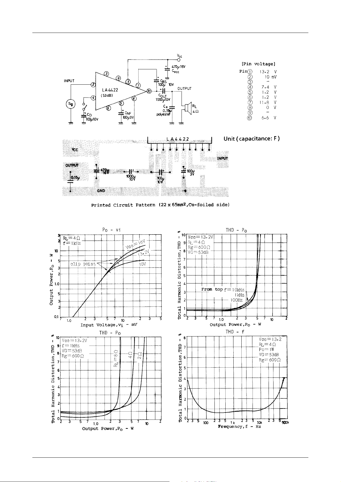
Sample Application Circuit 1. Power amplifier for 5.8W typ. car radio, car stereo
No.556–4/10
Page 5
LA4422
No.556–5/10
Page 6
LA4422
No.556–6/10
Page 7
LA4422
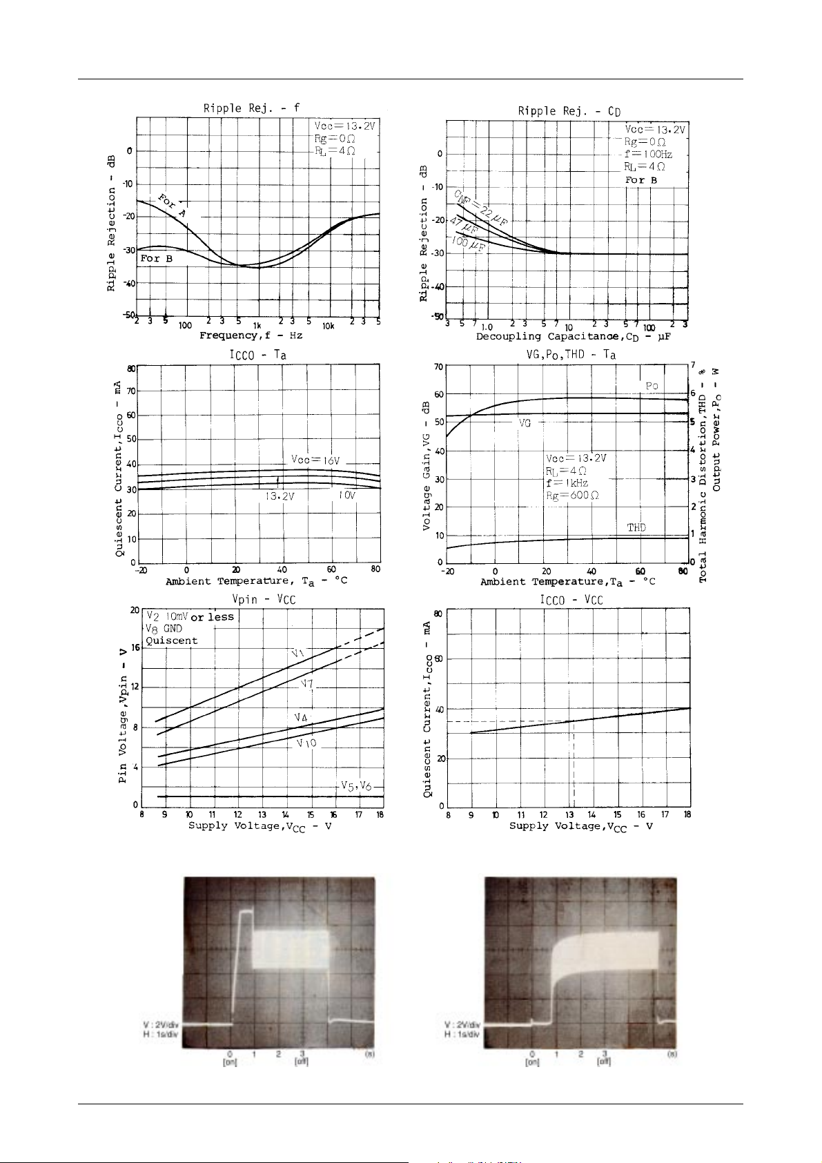
Output wave form (pop noise) influenced by CD/VCC=13.2V, RL=4Ω, f=1kHz, VO=1V
(1) CNF==100µF, perfect discharge (2) CNF=100µF, CD=100µF
No.556–7/10
Page 8
LA4422
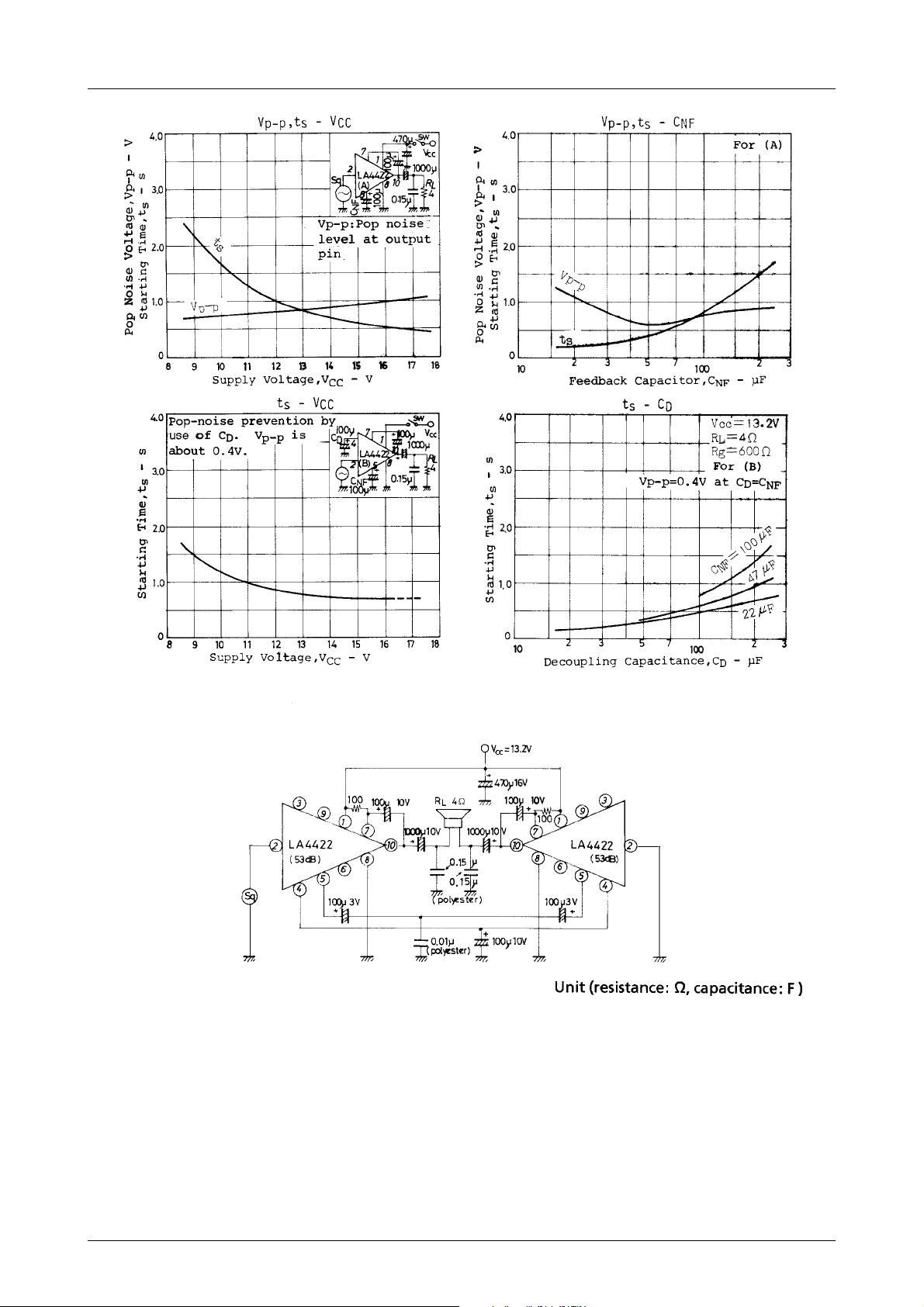
Sample Application Circuit 2. 18W typ. (VCC=13.2V, RL=4Ω) BTL amplifier
No.556–8/10
Page 9
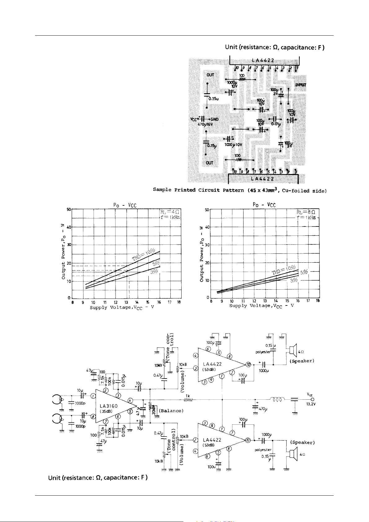
The heat sink design of this circuit is so
important that it is requested that you
should consult us beforehand.
LA4422
Sample Application Circuit 3. Pre-power amplifier for car stereo (4.75cm/s. cassette).
No.556–9/10
Page 10
LA4422
Proper Cares in Bridge Amplifier Application
For bridge amplifier design, take the following into consideration and consult our sales department.
· The LA4422 contains the thermal shutdown circuit which senses generation of abnormal heat attrib utable to load short,
etc. and stops the internal circuit operation. Thus, breakdown attributable to generatin of abnormal heat is prevented.
· This function operates normally for single IC operation, but the following extraordinary phenomena appear for bridge
operation.
a) Generation of heat of non-inverting, inverting amplifier ICs at the time of output non-clip depends on the radiation
condition of each IC.
b) Generation of heat at the time of output clip is always larger for in v erting amplifier IC, w hich cannot be compensated
even if there is slight difference of radiation condition between two ICs. This is because the output of non-inverter
amplifier IC is clipped and enters completely into the saturation region and Pd (power dissipation) is reduced, while
the output clip of inverting amplifier IC is a mere amplification of output (clip waveform) of non-inverter amplifier
and does not enter into the saturation region and Pd (power dissipation) is held somewhere at the max. level.
c) For this reason, the inverting amplifier IC always generates more heat at the time of output clip. If the radiation
condition is not designed correctly, the thermal shutdouwn circuit of inverting amplifier starts operating earlier.
d) For single IC operation, as above-mentioned, when the thermal shutdown circuit operates, not only the output signal
but also Pd (power dissipation) is reduced so as to minimize generation of heat.
For bridge operation also, if the thermal shutdown circuit of non-inverting amplifier IC operates earlier than the
inverting amplif ier IC, generation of heat is minimized similarly to the single IC operation. This is because reduction
of output of input side amplifier (inv erting IC) causes reduction of the total output. (It is almost impossible to realize
this state with the normal radiation design.) To the contrary, if the thermal shutdown circuit of inverting amplifier IC
operates earlier, the output of this inverting amplifier IC is reduced, but Pd (power dissipation) is not reduced due to
the drive from the output pin because of bridge connection and operation outside the ASO (area of safety operation)
may occur.
e) Therefore, if the thermal shutdown circuit operates (inverting side) at the time of bridge operation, the above phe-
nomena occur, and if the applied voltage is high, breakdo wn of the IC be yond the ASO (area of safety operation) may
result.
f) As seen from the above, it is one of the most important factors in the bridge operation circuit design that the radiation
design should be made to prevent the thermal circuit from operating.
Specifications of any and all SANYO products described or contained herein stipulate the performance,
characteristics, and functions of the described products in the independent state, and are not guarantees
of the performance, characteristics, and functions of the described products as mounted in the customer's
products or equipment. To verify symptoms and states that cannot be evaluated in an independent device,
the customer should always evaluate and test devices mounted in the customer's products or equipment.
SANYO Electric Co., Ltd. strives to supply high-quality high-reliability products. However, any and all
semiconductor products fail with some probability. It is possible that these probabilistic failures could
give rise to accidents or events that could endanger human lives, that could give rise to smoke or fire,
or that could cause damage to other property. When designing equipment, adopt safety measures so
that these kinds of accidents or events cannot occur. Such measures include but are not limited to protective
circuits and error prevention circuits for safe design, redundant design, and structural design.
In the event that any or all SANYO products(including technical data,services) described or
contained herein are controlled under any of applicable local export control laws and regulations,
such products must not be exported without obtaining the export license from the authorities
concerned in accordance with the above law.
No part of this publication may be reproduced or transmitted in any form or by any means, electronic or
mechanical, including photocopying and recording, or any information storage or retrieval system,
or otherwise, without the prior written permission of SANYO Electric Co. , Ltd.
Any and all information described or contained herein are subject to change without notice due to
product/technology improvement, etc. When designing equipment, refer to the "Delivery Specification"
for the SANYO product that you intend to use.
Information (including circuit diagrams and circuit parameters) herein is for example only ; it is not
guaranteed for volume production. SANYO believes information herein is accurate and reliable, but
no guarantees are made or implied regarding its use or any infringements of intellectual property rights
or other rights of third parties.
This catalog provides information as of February, 2000. Specifications and information herein are subject
to change without notice.
PS No.556–10/10
 Loading...