

Page 1
Ordering number: EN5376
Monolithic Linear IC
LA5314
Variable Divided Voltage Generator
for LCD Use
Overview
The LA5314 is a valiable diveded voltage generator IC for
multiple drive of LCD matrix.
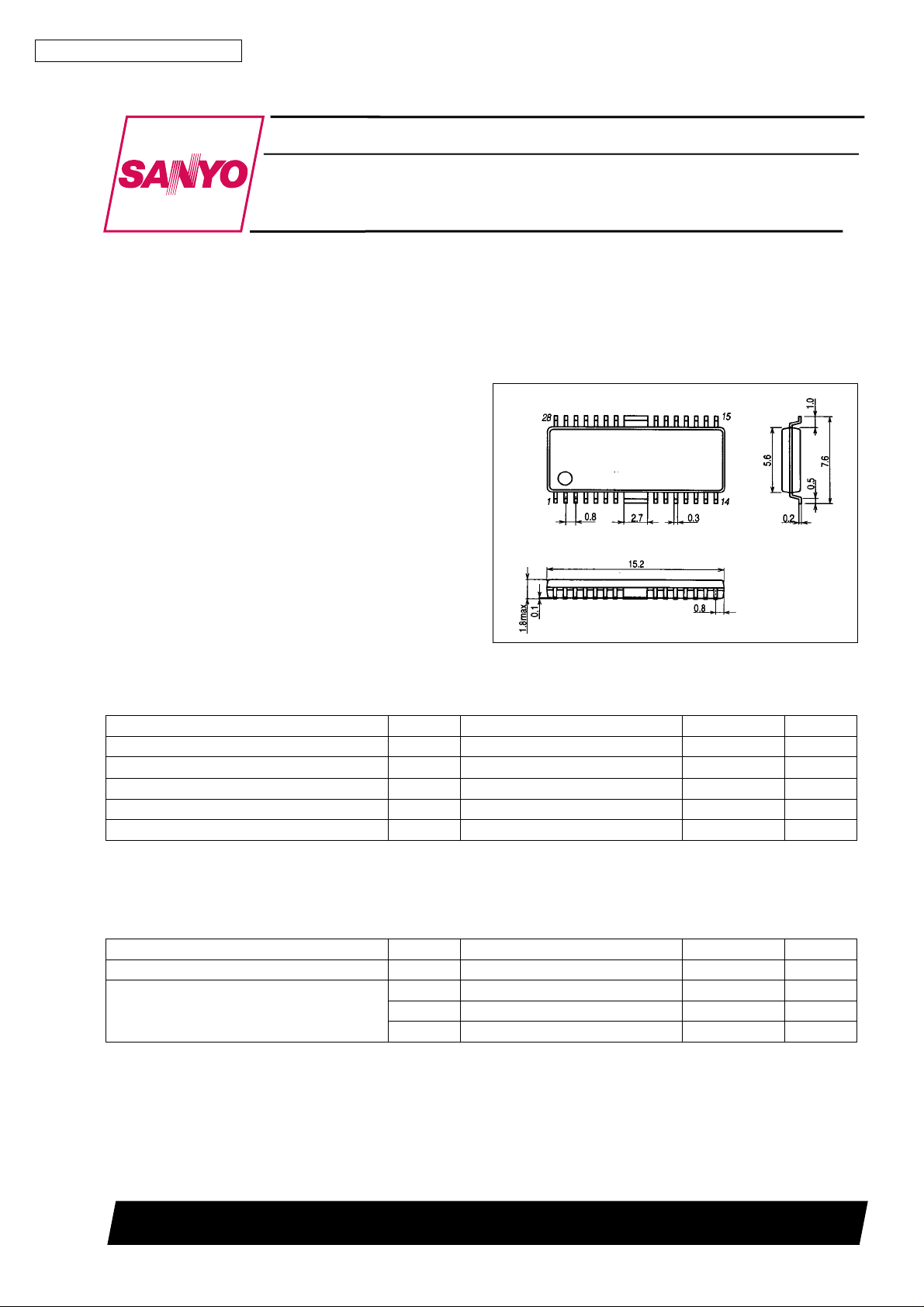
Package Dimensions
unit : mm
3222-HSOP28
[LA5314]
Features
.
Power supply for variable bias LCD matrix. (1/5 to 1/20 bias
available by built-in resistances)
.
Five operational amplifiers to deliver 5 voltage outputs
.
Low current drain (1.6 mA typ)
.
Miniflat package for miniturization
SANYO : HSOP28
Specifications
Maximum Ratings atTa=25°C
Parameter Symbol Conditions Ratings Unit
Maximum supply voltage V
Maximum output current l
Allowable power dissipation Pd max 600 mW
Operating temperature Topr –20 to +75 °C
Storage temperature Tstg –30 to +150 °C
max VCC–V
CC
max V0 to V4
OUT
EE
38 V
*±25
mA
Note: 1. Continuous operation (non breakdown) is guaranteed when operated at the maximum ratings shown above.
2. *The maximum output current is a value specified under the conditions otherwise specified separately.
Operating Conditions at Ta = 25°C
Parameter Symbol Conditions Ratings Unit
Supply voltage V
l
OUT
Output current
Note: 3. Set VCCand VEEso that |V0–V1| and |V4| become 1V or greater.
l
OUT
l
OUT
VCC–V
CC
0, 1 V0, V1 –0.5 to +10 mA
2, 3 V2, V3 –10 to +10 mA
4 V4 –15 to +0.5 mA
EE
10 to 35 V
SANYO Electric Co.,Ltd. Semiconductor Bussiness Headquarters
TOKYO OFFICE Tokyo Bldg., 1-10, 1 Chome, Ueno, Taito-ku, TOKYO, 110 JAPAN
83096HA(II) No.5376-1/5
Page 2
LA5314
Operating Chararcteristics at Ta = 25°C, VCC– VEE= 20 V, V
Parameter Symbol Conditions min typ max Unit
Current drain I
Output voltage difference 1 Vd1 (V0 – V1) – (V1 – V2) –30 +30 mV
Output voltage difference 2 Vd2 (V3 – V4) – (V4 – V
Output voltage ratio 1 Rb1 V0/(V0 – V1) 11.64 12.00 12.36 —
Output voltage ratio 2 Rb2 V0/(V0 – V2) 5.82 6.00 6.18 —
Output voltage ratio 3 Rb3 V0/V3 5.82 6.00 6.18 —
Output voltage ratio 4 Rb4 V0/V4 11.64 12.00 12.36 —
Internal resistnace ratio 1 8R R
Internal resistance ratio 2 12R R
Internal resistance ratio 3 14R R
Internal resistance ratio 4 15R R
Resistance R
Load regulation 1 ∆V0 V0: –0.2 mA < I
Load regulation 2 ∆V1 V1: –0.2 mA < I
Load regulation 3 ∆V2 V2: –10.0 mA < I
Load regulation 4 ∆V3 V3: –10.0 mA < I
Load regulation 5 ∆V4 V4: –10.0 mA < I
CC,IEE
VCC,VEE:VCC–VEE=20V,RX= 8R 1.6 3 mA
) –30 +30 mV
EE
1–RX2* 8—
X
1–RX3* 12 —
X
1–RX4* 14 —
X
1–VIN3* 15 —
X
R value when 0.6 V is applied across R
R
5–RX6
X
0 < +10.0 mA –20 +20 mV
OUT
1 < +10.0 mA –20 +20 mV
OUT
2 < +10.0 mA –20 +20 mV
OUT
3 < +10.0 mA –20 +20 mV
OUT
4 < +0.2 mA –20 +20 mV
OUT
= VCC, RX= 8R
REF
5–RX6:
X
20 kΩ
Note* : Referenced to R between RX4 and VIN3
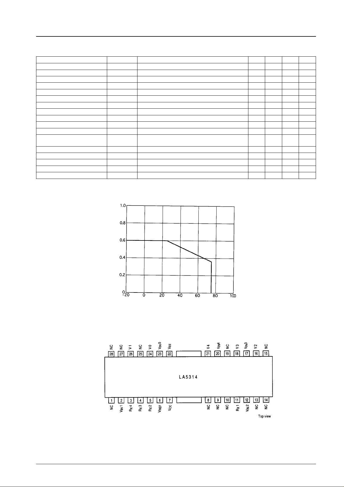
Pd max — Ta
Pin Assignment
Allowable power dissipation, Pd max — W
Temperature, Ta —°C
T00025
No.5376-2/5
Page 3

Block Diagram
LA5314
Note: Use the IC so that VRX1 ^ VRX2 ^ VRX3 ^ VRX4 is obeyed.
No.5376-3/5
Page 4
LA5314
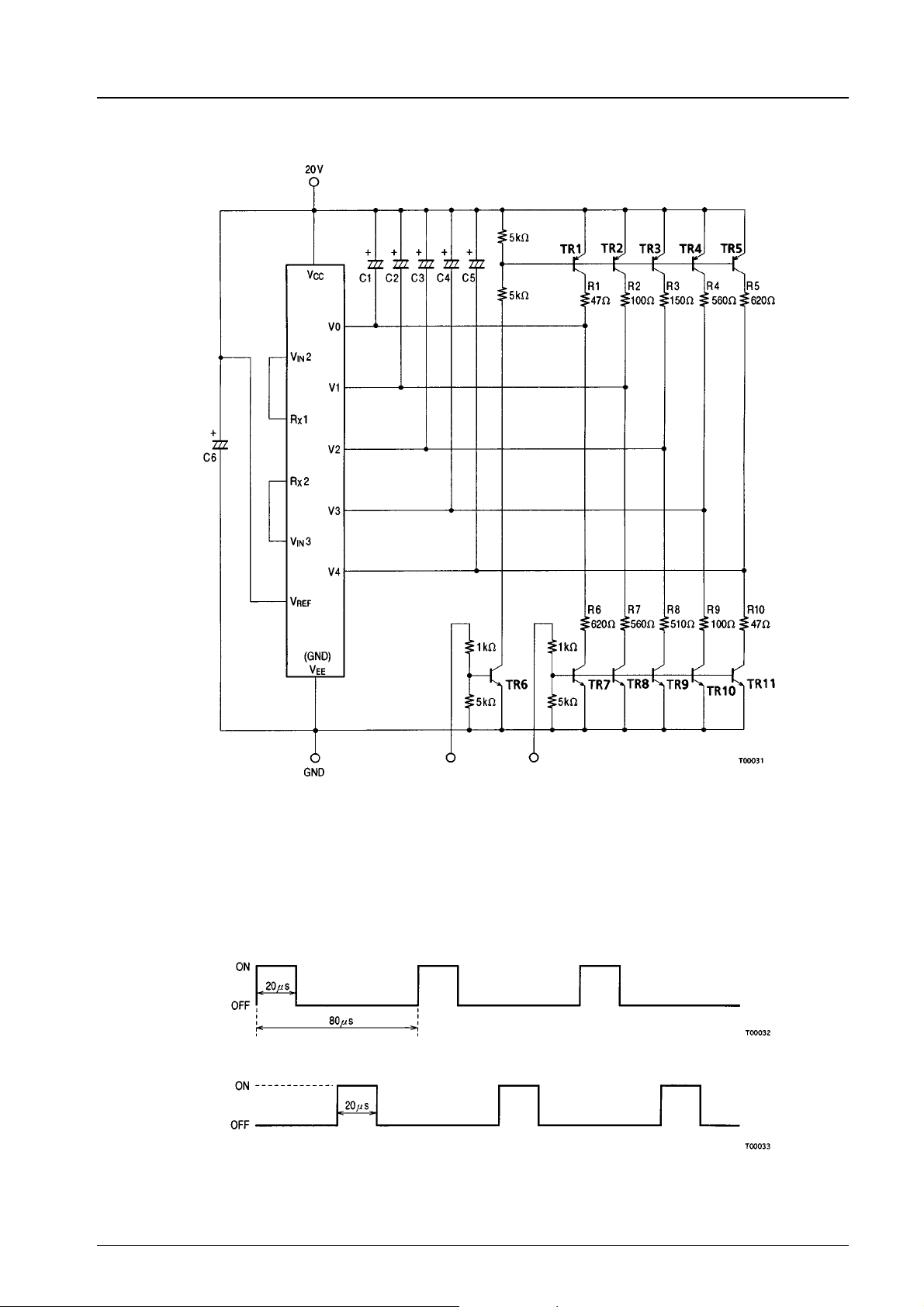
Maximum Output Current Load Test Conditions
Input 1
V
CC–VEE
C1=5µF,C2=10µF,C3=10µF,C4=5µF,C5=10µF,C6=33µF
TR1 to TR5: 2SA984 E or F rank
TR6 to TR11: 2SC2274 E or F rank
Output load resistances R1 to R10 are set in order that current of 30 mA max. are supplied to both source and sink sides when an
on-level input is applied to the inputs 1 or 2.
=20V,RX=8R
Input 1
Input 2
Input 2
Unit (resistance: Ω, capacitance: F)
No.5376-4/5
Page 5
LA5314
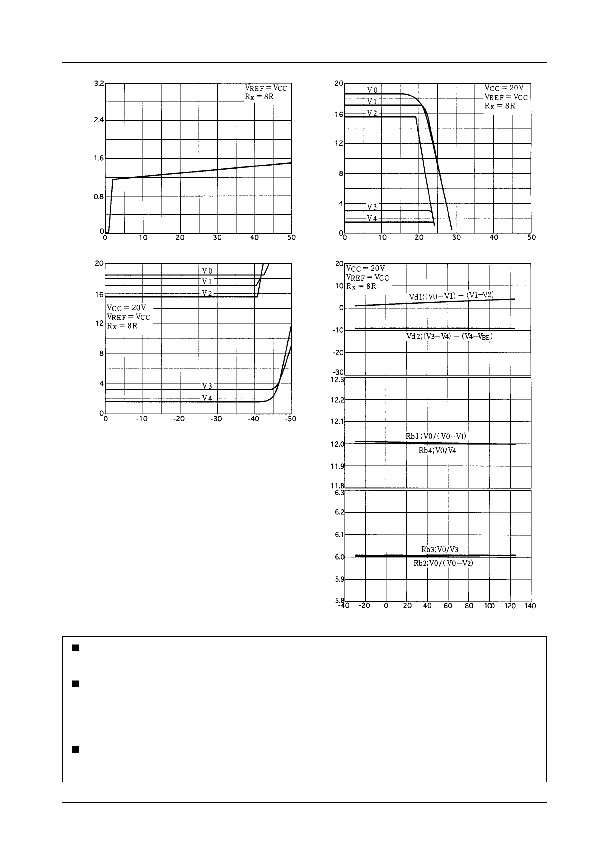
–mA
CC
Current drain, I
–V
OUT
ICC–V
CC
Supply voltage, VCC–V
V
OUT–IOUT
(Sink side)
–V
OUT
Output voltage, V
V
OUT–IOUT
Output current, I
(Source side)
–mA
OUT
Output voltage ratio – Ta
Output voltage difference , Vd1, Vd2 — mVOutput voltage ratio, Rb1, Rb4
Output voltage , V
Output current, I
OUT
–mA
Output voltage ratio, Rb2, Rb3
Ambient temperature, Ta – °C
No products described or contained herein are intended for use in surgical implants, life-support systems, aerospace equipment,
nuclear power control systems, vehicles, disaster/crime-prevention equipment and the like, the failure of which may directly or
indirectly cause injury, death or property loss.
Anyone purchasing any products described or contained herein for an above-mentioned use shall:
1 Accept full responsibility and indemnify and defend SANYO ELECTRIC CO., LTD., its affiliates, subsidiaries and distributors
and all their officers and employees, jointly and severally, against any and all claims and litigation and all damages, cost and
expenses associated with such use:
2 Not impose any responsibility for any fault or negligence which may be cited in any such claim or litigation on SANYO
ELECTRIC CO., LTD., its affiliates, subsidiaries and distributors or any of their officers and employees jointly or severally.
Information (including circuit diagrams and circuit parameters) herein is for example only; it is not guaranteed for volume
production. SANYO believes information herein is accurate and reliable, but no guarantees aremadeorimpliedregardingitsuse
or any infringements of intellectual property rights or other rights of third parties.
This catalog provides information as of August, 1996. Specifications and information herein are subject to change without notice.
No.5376-5/5
 Loading...