

Page 1

Overview
The LA4585M is a preamplifier plus power amplifier IC
that supports auto-reverse and was developed for use in
3-V headphone stereo products.
Features
• The LA4585M is designed for use in playback-only
compact cassette players. In addition to preamplifier and
power amplifier functions, the LA4585M also provides
low boost and automatic power output limiter
(PVSS:Peak Volume Select System) functions.
• Provided in a mini-flat 36-pin quad package (0.65 mm
lead pitch) optimal for miniature end products.
• Two auto-reverse playback preamplifiers
• Two headphone power amplifiers (16 Ω)
• Low boost function (auto-loudness effect)
• Output limiter function (PVSS)
• Two radio input switches (pre-muting switches)
• Power muting switch
Package Dimensions
unit: mm
3162B-QFP36
Monolithic Linear IC
Ordering number : EN5661
73097HA(OT) No. 5661-1/5
SANYO: QFP36
[LA4585M]
SANYO Electric Co.,Ltd. Semiconductor Bussiness Headquarters
TOKYO OFFICE Tokyo Bldg., 1-10, 1 Chome, Ueno, Taito-ku, TOKYO, 110 JAPAN
3-V Preamplifier + Power Amplifier for
Headphone Stereo Products
LA4585M
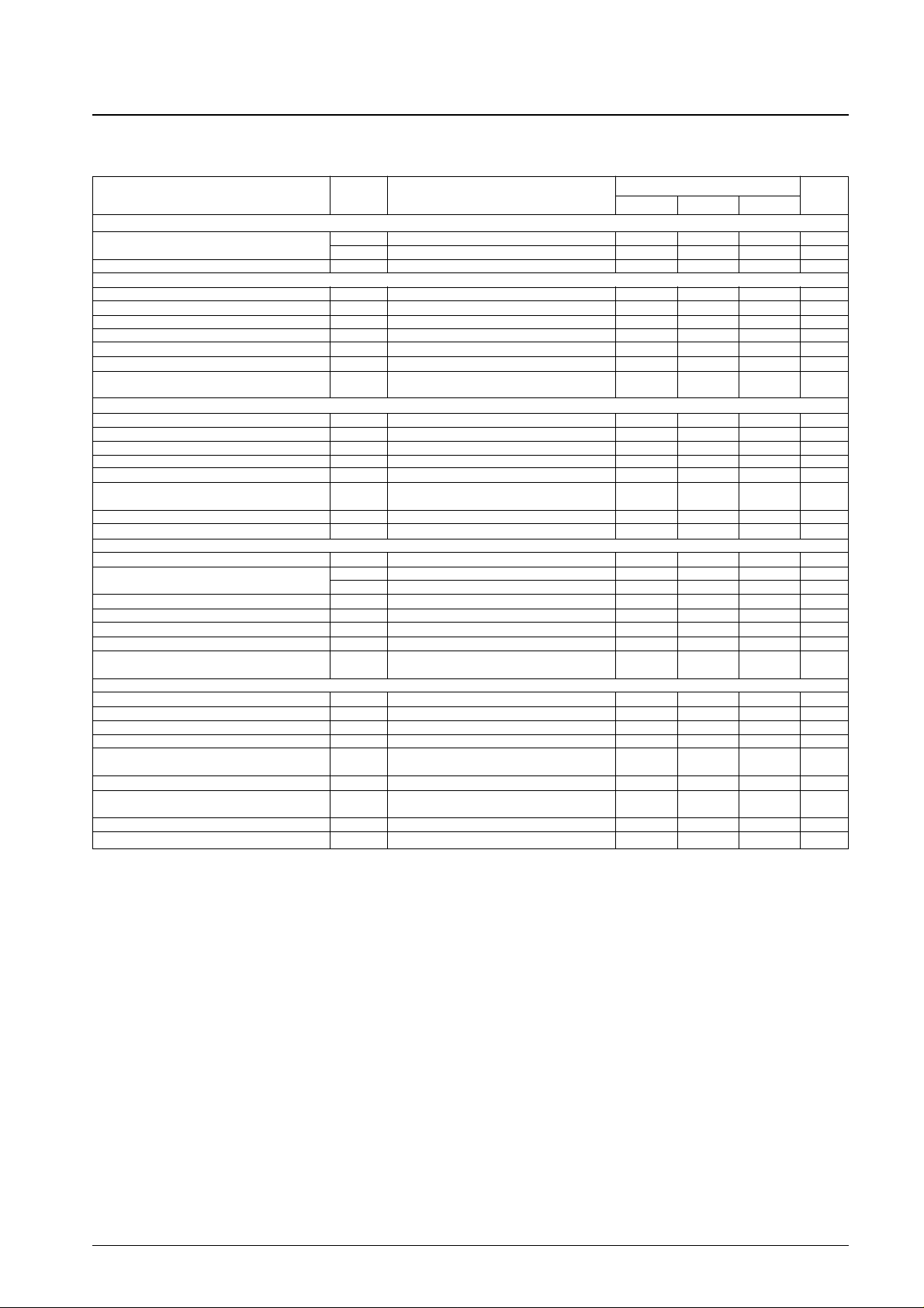
Parameter Symbol Conditions Ratings Unit
Maximum supply voltage V
CC
max 4.5 V
Allowable power dissipation Pd max 375 mW
Operating temperature Topr –20 to +75 °C
Storage temperature Tstg –40 to +150 °C
Specifications
Maximum Ratings at Ta = 25°C
Parameter Symbol Conditions Ratings Unit
Recommended supply voltage V
CC
3.0 V
Operating supply voltage range V
CC
op 1.8 to 3.6 V
Operating Conditions at Ta = 25°C
Ambient temperature, Ta – °C
Allowable power dissipation, Pd max – mW
Page 2
No. 5661-2/5
LA4585M
Parameter Symbol Conditions
Ratings
Unit
min typ max
[PRE + LOW BOOST + PVSS + PWR]
Quiescent current
I
CCO
1 Rg = 2.2 kΩ, low boost off, PVSS off 12 15 21 mA
I
CCO
2 Rg = 2.2 kΩ, low boost on, PVSS on 12 15 21 µA
Voltage gain (closed loop) VG
TVO
= –5 dBm 62 64 67 dB
[PRE AMP]
Voltage gain (open loop) VG
0VO
= –5 dBm 70 83 dB
Voltage gain (closed loop) VG1 V
O
= –5 dBm 40 dB
Maximum output voltage V
O
max1 THD = 1 %, VCC= 1.8 V 0.1 0.2 V
Total harmonic distortion THD1 V
O
= 0.2 V, VG = 40 dB/NAB 0.05 0.5 %
Equivalent input noise voltage V
NI
Rg = 2.2 kΩ, BPF = 20 Hz to 20 kHz 1.3 2.0 µV
Crosstalk CT1 Rg = 2.2 kΩ, TUNE 1 kHz 60 80 dB
Ripple rejection ratio SVRR
Rg = 2.2 kΩ, V
CC
= 1.8 V, Vr = –20 dBm,
40 50 dB
fr = 100 Hz
[POWER AMP]
Output voltage P
O
THD = 10 % 23 34 mW
Voltage gain VG2 V
O
= –5 dBm 27 29 32 dB
Total harmonic distortion THD2 P
O
= 1 mW 0.4 1.0 %
Interchannel crosstalk CT2 V
O
= –5 dBm, RV= 0 Ω 30 40 dB
Output noise voltage V
NO
1 RV= 0 Ω, BPF = 20 Hz to 20 kHz 25 40 µV
Ripple rejection ratio Rr2
R
V
= 0 Ω, Vr = –20 dBm,
45 55 dB
fr = 100 Hz, VCC= 1.8 V
Input resistance Ri 22 30 38 kΩ
DC offset voltage V
ODC OFF
Between pin 6 and pins 4 and 8 –90 +90 mV
[LOW BOOST]
Voltage gain VG3 Vi = –30 dBm, boost on/off –2.3 –3.8 –5.3 dB
Boost*
BST1 Vi
BST
= –30 dBm, f = 100 Hz, boost on 11.2 14.7 18.2 dB
BST2 Vi
BST
= –30 dBm, f = 10 kHz, boost on 7.0 8.5 10 dB
Maximum output voltage V
O
max2 THD = 1%, boost on 0.25 0.4 V
Total harmonic distortion THD3 V
O
= 0.1 V, boost on 0.1 0.5 %
Interchannel crosstalk CT3 V
O
= –20 dBm, Rg = 0, boost on 25 32 dB
Output noise voltage V
NO
2 Rg = 0, BPF = 20 Hz to 20 kHz, boost on 2.0 5.0 µV
Ripple rejection ratio Rr3
Rg = 0, f
R
= 100 Hz, VR= –20 dBm,
45 53 dB
VCC= 1.8 V, boost on
[LOW BOOST + PVSS + POWER] The following items are measured at an R
V
of 10 kΩ maximum.
Voltage gain VG4 Vi = –40 dBm, f = 1 kHz, boost off/on 22 24 27 dB
LOW BOOST output voltage V
O
1 Vi = –43 dBm, f = 100 Hz, boost on 0.13 0.23 0.33 V
LOW BOOST output voltage V
O
2 Vi = –28 dBm, f = 100 Hz, boost on 0.25 0.40 0.55 V
LOW BOOST total harmonic distortion THD4 Vi = –40 dBm, f = 100 Hz, boost on 0.5 1.2 %
Output noise voltage V
NO
3
Rg = 0, CCIR-ARM, boost off, with the power
–88 –85 –82 dBm
input switch K18 set to B.
PVSS voltage V
O
3 Vi = –40 dBm, PVSS 2 –40 –37 –34 dBm
PVSS width W
PVSS
The input amplitude between the start point and
30 40 dB
the point where the output is +4 dB. PVSS on
PVSS harmonic distortion THD5 Vi = –40 dBm, PVSS 2 0.5 1.2 %
PVSS start input level V
OPi
PVSS 2 –67 –63 –59 dBm
Operating Characteristics at Ta = 25°C, VCC= 3.0 V, fi = 1 kHz, 0.775 = 0 dBm, preamplifier RL= 10 kΩ,
low boost, power amplifier RL= 10 Ω
Note: *The amount of boost for a 1-kHz input.
Page 3
No. 5661-3/5
LA4585M
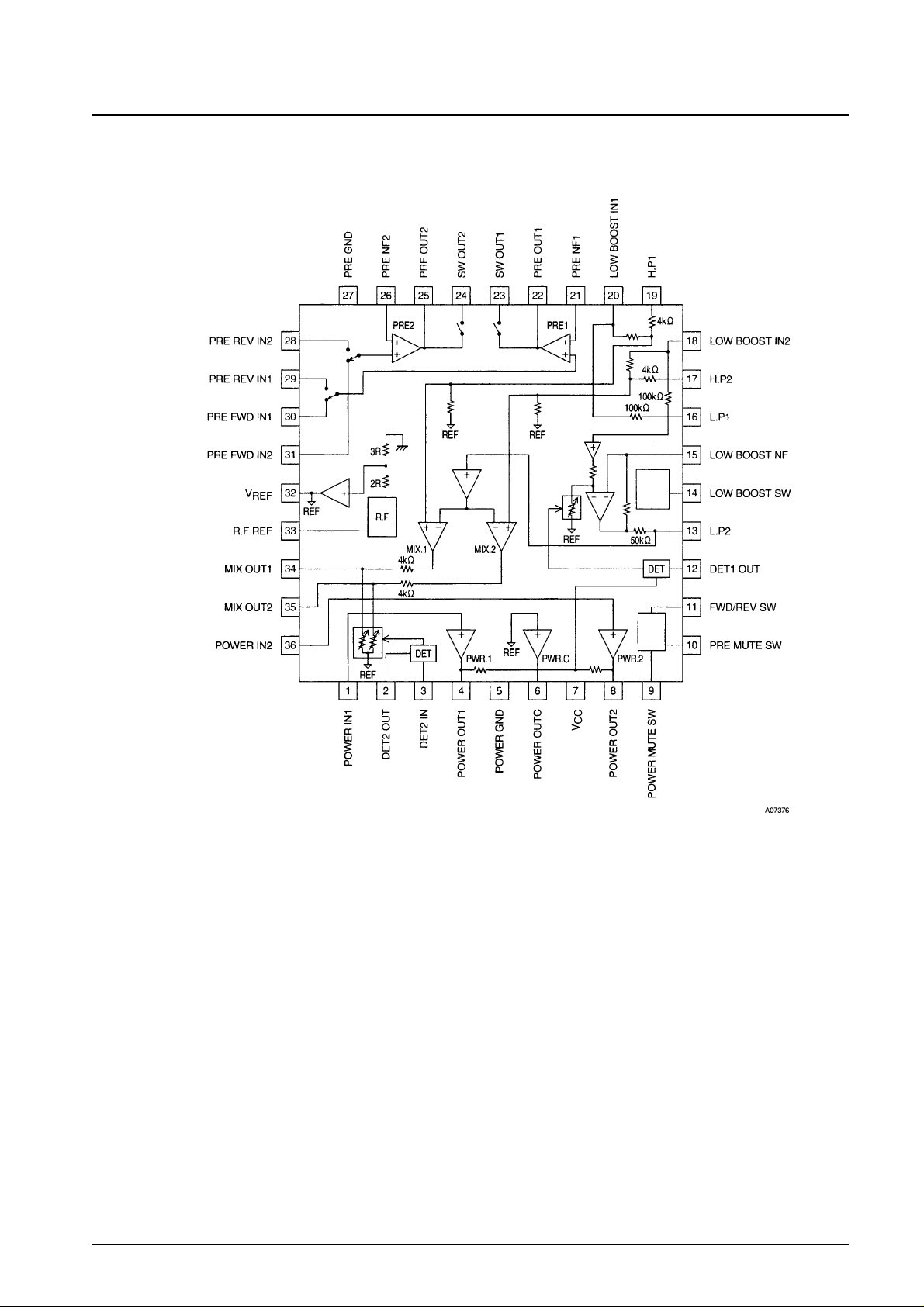
Block Diagram
Low
boost
Sys.
cont
Page 4
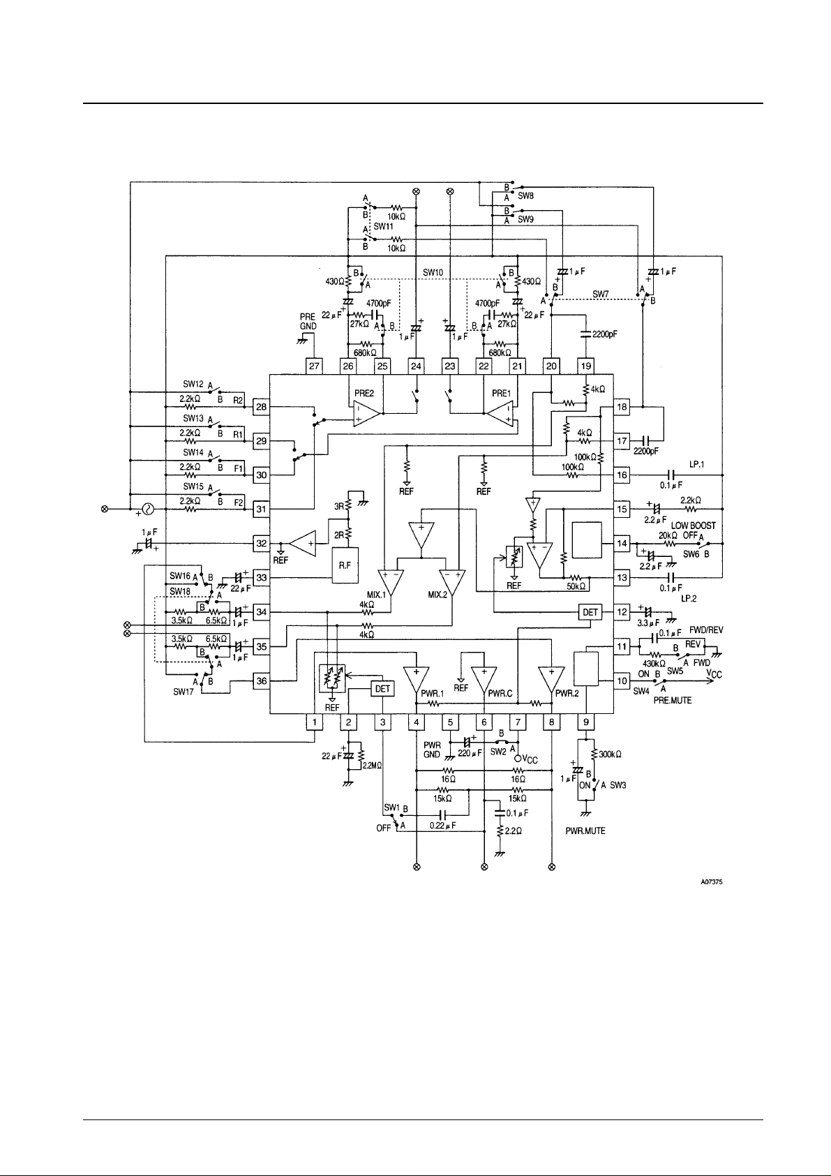
Test Circuit Diagram
No. 5661-4/5
LA4585M
Low
boost
Sys.
cont
Page 5
No. 5661-5/5
LA4585M
This catalog provides information as of July, 1997. Specifications and information herein are subject to change
without notice.
■ No products described or contained herein are intended for use in surgical implants, life-support systems, aerospace
equipment, nuclear power control systems, vehicles, disaster/crime-prevention equipment and the like, the failure of
which may directly or indirectly cause injury, death or property loss.
■ Anyone purchasing any products described or contained herein for an above-mentioned use shall:
➀ Accept full responsibility and indemnify and defend SANYO ELECTRIC CO., LTD., its affiliates, subsidiaries and
distributors and all their officers and employees, jointly and severally, against any and all claims and litigation and all
damages, cost and expenses associated with such use:
➁ Not impose any responsibility for any fault or negligence which may be cited in any such claim or litigation on
SANYO ELECTRIC CO., LTD., its affiliates, subsidiaries and distributors or any of their officers and employees
jointly or severally.
■ Information (including circuit diagrams and circuit parameters) herein is for example only; it is not guaranteed for
volume production. SANYO believes information herein is accurate and reliable, but no guarantees are made or implied
regarding its use or any infringements of intellectual property rights or other rights of third parties.
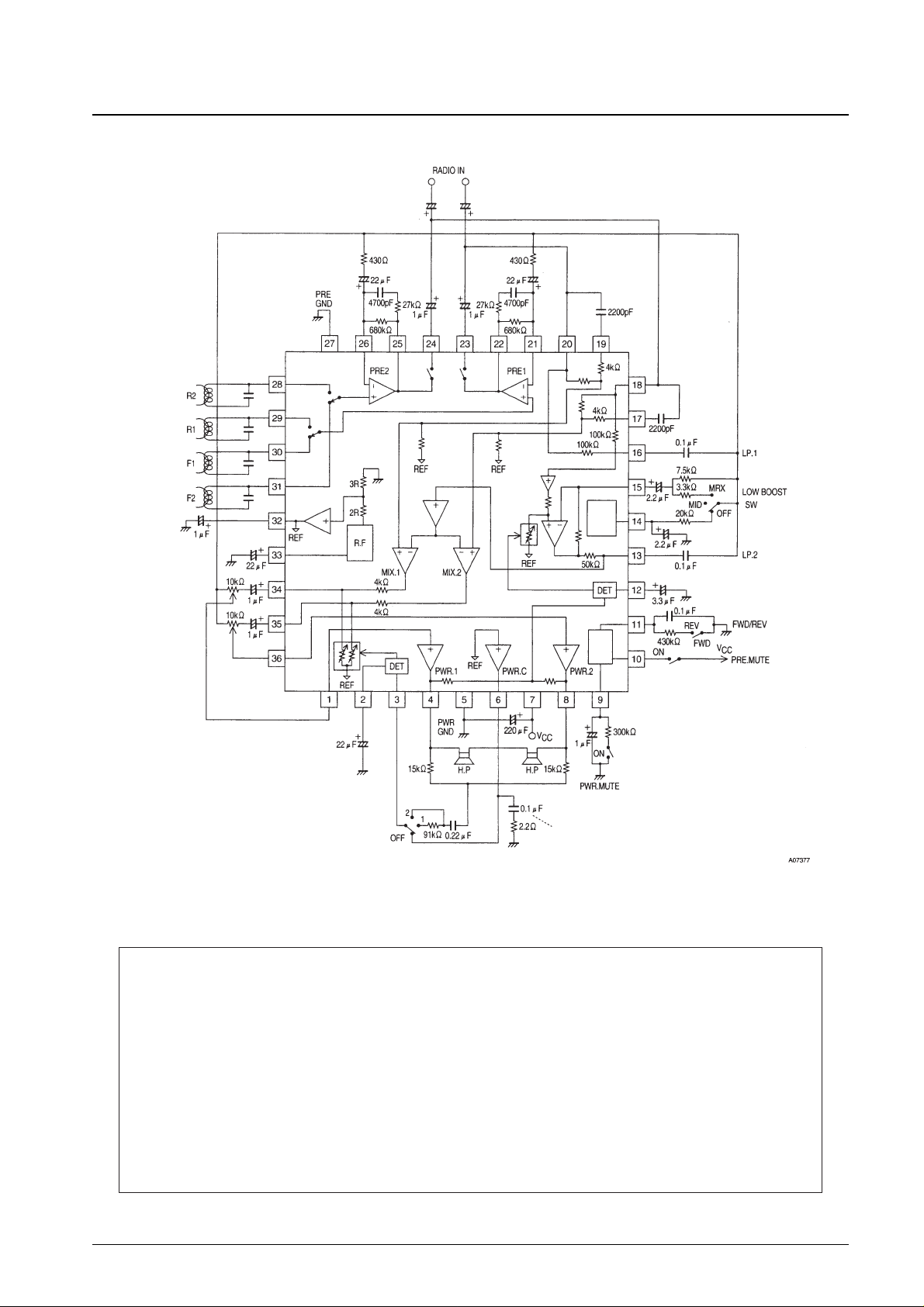
Sample Application Circuit
The use of polyester film or ceramic
capacitors is recommended. However,
capacitors whose capacitances are
guaranteed for the operating temperature
range of the end product should be used.
Low
boost
Sys.
cont
 Loading...