

Page 1
Ordering number : EN6012
LA4600
Monolithic Linear IC
LA4600
..
Overview
The LA4600 is an audio power amplifier which
requires minimum count of external parts by
incorporating BS capacitor, NF capacitor; and
oscillation prevention CR components into the IC
circuitry .
Functions
• Output power : V
V
• Built-in stanby switch
• Built-in overheat protection (TSD)
= 12V/4Ω............ 4.0W X 2
CC
= 9V/4Ω .............. 2.0W X 2
CC
Audio Power Amplifier for
Radio Cassette Recorders
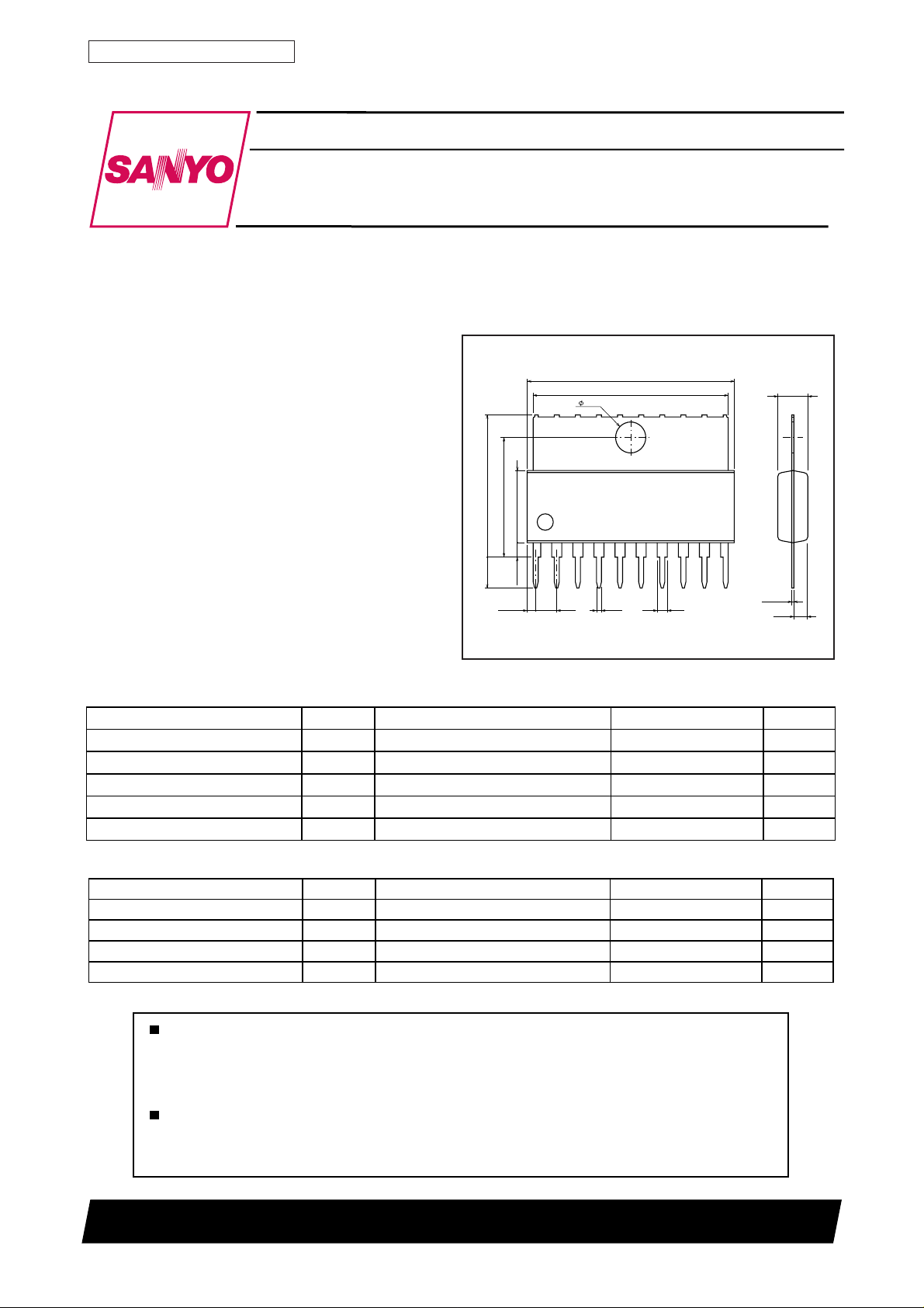
Package Dimensions
unit: mm
3046B-SIP10F
[LA4600]
25.5
24.0
3.6
16.7max
14.0
8.4
3.5
1.6min
1.32
2.54
0.5
1.3
3.6
101
0.45
1.6
SANYO : SIP10F
Specifications
Maximum Ratings at Ta = 25
Parameter Symbol Conditions Ratings Unit
Maximum supply voltage Vcc
Allowable power dissipation Pd max With an arbitrary large 12.5 W
Thermal resistance
Operating temperature Topr °C
Storage temperature Tstg °C
Operating Conditions at Ta = 25°C
Parameter Symbol Conditions Ratings Unit
Recommended supply voltage Vcc 12 V
Recommended load resistance
Operating supply voltage range Vcc
Operating load resistance range Ω
Any and all SANYO products described or contained herein do not have specifications that can handle
applications that require extremely high levels of reliability, such as life-support systems, aircraft's
control systems, or other applications whose failure can be reasonably expected to result in serious
physical and/or material damage. Consult with your SANYO representative nearest you before using
any SANYO products described or contained herein in such applications.
SANYO assumes no responsibility for equipment failures that result from using products at values that
exceed, even momentarily, rated values (such as maximum ratings, operating condition ranges, or other
parameters) listed in products specifications of any and all SANYO products described or contained
herein.
°C
max Rg=0 (No signal) 24 V
θj-c
R
L
Op Within maximum ratings V
10.0 °C/W
– 20 to +75
– 40 to +150
4 Ω
5.0 to 22
2.7 to 8
SANYO Electric Co., Ltd. Semiconductor Business Headquarters
TOKYO OFFICE Tokyo Bldg., 1-10, 1 Chome, Ueno, Taito-ku, TOKYO, 110-8534 JAPAN
N1298RM(KI)
No. 6012-1/7
Page 2
LA4600
Electrical Characteristics at Ta = 25°C, VCC=12V, RL=4Ω , f=1 kHz
Parameter
Standby current Is t Standby pin —> GND 1.0 10 µA
Quiescent current Icco Rg=0 18 32 64 mA
Voltage gain VG Vo=0dBm 43.0 45.0 47.0 dB
Total harmonic distortion THD Po=1w 0.2 0.8 %
Output noise voltage Vno Rg=0, DIN AUDIO 0.15 0.5 mV
Output voltage Po1 THD=10% 3.0 4 .0 W
Channel separation Chsep Vo=0dBm, Rg=0, DIN AUDIO 50 60 dB
Ripple rejection ratio SVRR Vr=0dBm, Rg=0, fr=100 Hz DIN AUDIO 45 55 dB
Stanby ON voltage Vst 1.5 5.0 V
Input resistance Ri 20 30 4 0 KΩ
Symbol
Po2 Vcc=9V, THD=10% 1.5 2.0 W
Conditions Unit
min typ max
Ratings
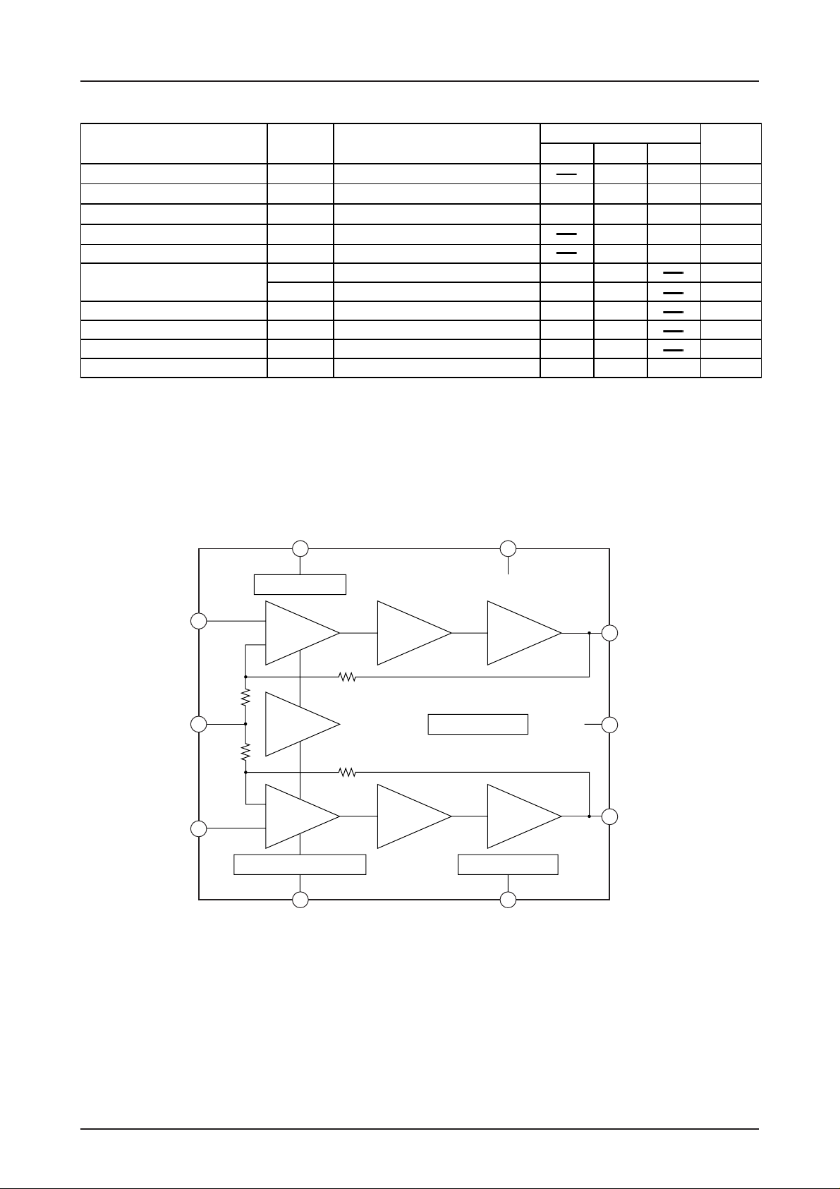
Block Diagram
CH1 input
Small signal
GND
CH2 input
10
Standby
7
Standby switching
CH1 input
amplifier
R
Nf1
9
R
Nf2
8
REF
amplifier
CH2 input
amplifier
Pop noise prevention block
6 5
P.P
Predrive
amplifier
R
f1
TSD protector
R
f2
Predrive
amplifier
Vcc
4
Output
amplifier
Output
amplifier
Ripple filter
Filter
CH1 output
1
Large signal
2
GND
CH2 output
3
No. 6012-2/7
Page 3
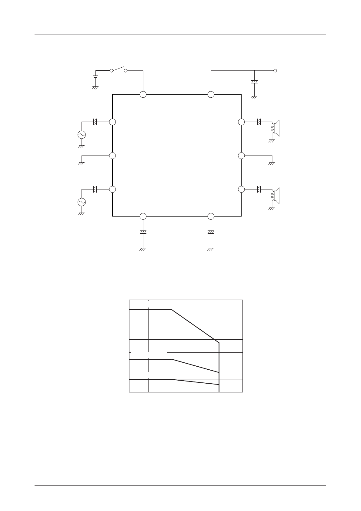
Sample Application
LA4600
+5V
0.22µF
0.22µF
+
1000µF
7
STANDBY
+
ch1
10
Input
PRE GND
9
+
ch2
8
Input
LA4600
4
V
CC
Output
POWER GND
Output
ch1
ch2
+
1
1000µF
4Ω
2
+
3
1000µF
4Ω
P.P Filter
6
+
4.7µF 100µF
5
+
14
With an arbitrary large heatsink (θjc=10˚C/W)
12
10
8
6
50X50X1.5mm
5
4
No heatsink
2
Allowable power dissipation, Pd max – W
0
–20 0 20 40 60 80 100
Pd max – Ta
12.5
3
1.94
7.5
3.0
1.16
Ambient temperature, Ta – ˚C
No. 6012-3/7
Page 4

Pin Descriptions
LA4600
1. Standby switching function (7)
V
CC
Power is switched ON and OFF by controlling the High and Low states at pin
7, respectively (standby). To switch power ON, apply 1.5V or more, or 800
To bias circuit
µA to pin 7.
Current supplied to pin 7
Applied voltage
.
=
.
Applied voltage – V
+
2 kΩ
• When directly connecting a microcontroller with this pin, add a resistor in series
(approx. 0.7V)
BE
2 kΩ
7
2kΩ
2kΩ
to optimize the current for the microcontroller.
2. Input pins (8,10)
Voltage at the input pins is approx. 2 V
Input impedance is approx. 30 kΩ.
• The recommended value for the input capacitor is 0.22 µF, but this can be varied in order to adjust the starting time
(t
). (The starting time is the time required from applying voltage to the standby pin until sound output is obtained. )
s
(1.4V).
BE
Input capacitator
Starting time (t
)
s
1.0 µF 2.0 µF 3.3 µF 4.7 µF 10 µF
0.2s 0.3s 0.5s 0.65s 1.5s
3. Filter (decoupling) pin (5)
Pin voltage is approx. 1/2 VCC.
The recommended value for the filter capacitor is 100 µF.
When capacitance is lower, pop noise when setting the standby pin to Low (power OFF) will increase.
Filter capacitor= 100 µ
AC voltage (100 mV)
Output DC voltage
AC voltage (200mV)
Output DC voltage
Filter capacitor= 47 µF
No. 6012-4/7
Page 5
LA4600
/
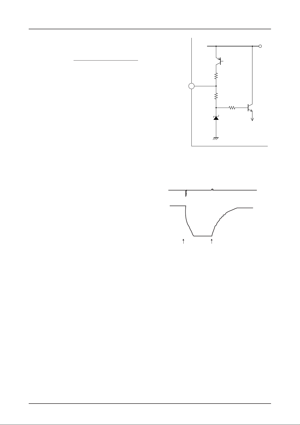
4. P.P (pop noise) pin (6)
V
– VCE (approx. 0.3V) – 5.6V
.
CC
Voltage at pin 6
=
.
2
5.6V
+
• The recommended value for the P.P capacitor is 4.7 µF.
When capacitance is lower than 2.2 µF, pop noise when setting the standby
pin to Low (power OFF) will increase.
When capacitance is higher than 10 µF, the sound will not be cut off when
setting the standby pin to Low (power OFF).
5. Muting
The output signal can be controlled by
connecting pin 5 (Filter) to ground via a
resistance of 300 to 500 Ω. If resistance
is higher than 750 Ω, the suppression
ratio will decrease.
Output AC voltage
Output DC voltage
V
CC
5kΩ
6
5kΩ
Zener voltage
= 5.6V
To input amplifier
bias circuitry
Mute ON Mute OFF
No. 6012-5/7
Page 6
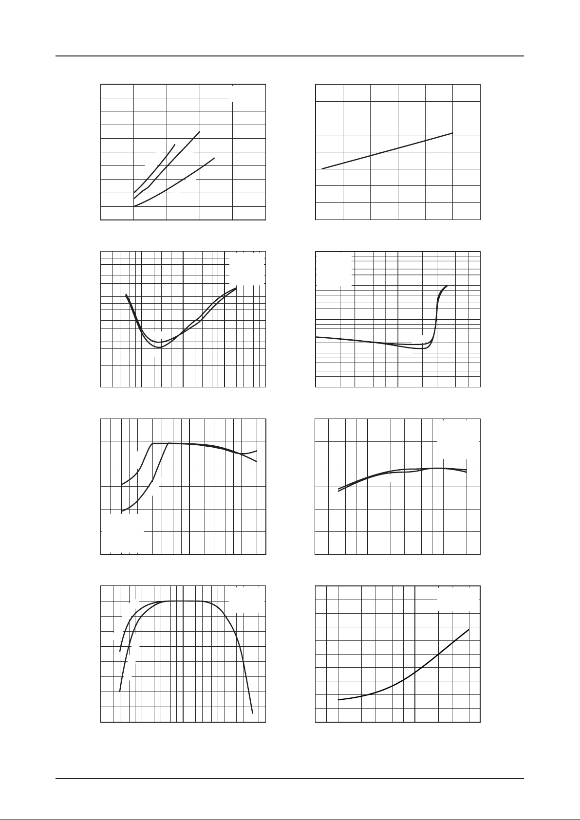
LA4600
10
9
8
7
– WTotal harmonic distortion, THD – %
O
6
5
4
3
Output power, P
2
1
0
4 8 12 242016
VCC – P
=3Ω
L
R
O
THD=10%
f=1kHz
=4Ω
L
R
=8Ω
L
R
80
70
60
– mA
CCO
50
40
30
20
Quiescent current, I
10
0
4 8 12 16 20 24 28
Supply Voltage, VCC – V
10
7
5
3
2
1.0
7
5
3
2
0.1
7
5
3
2
0.01
10 23 57 23 57 23 57 23 57100 1k 10k 100k 0.1 1.023 57 23 5710
THD – f
2ch
1ch
VCC=12V
RL=4Ω
PO=1W
Rg=600Ω
100
7
VCC=12V
5
RL=4Ω
3
PO=1W
2
Rg=600Ω
10
7
5
3
2
1.0
7
5
3
2
0.1
7
5
3
Total harmonic distortion, THD – %
2
0.01
Frequency, f – Hz
ch2-ch1
Chsep – f
80
70
60
50
80
70
60
50
VCC – I
Supply Voltage, V
THD – P
CCO
CC
O
1ch
2ch
Output power, PO – W
SVRR – f
ch1
ch2
–V
VCC=12V
RL=4Ω
Vr=0dBm
Rg=0
DIN AUDIO
Rg=0
ch1-ch2
40
VCC=12V
RL=4Ω
30
VO=0dBm
Channel separation, Chsep – dB
Rg=0
DIN AUDIO
20
3 100 2 3 5 7257 2357 231k 10k
Frequency, f – Hz
1
0
–1
–2
Cout=2200
–3
–4
Response – dB
–5
–6
–7
–8
10 2 3 5 7 2 3 5 7 2 3 5 7 2 3 5 7100 1k 10k 100k
f – Response
µF
µF
Cout=1000
VCC=12V
RL=4Ω
VO=0dBm
Frequency, f – Hz
40
Ripple rejection, SVRR – dB
30
20
3 100 2 3 5 7257 231k
Frequency, f – Hz
1.0
0.9
0.8
– mV
NO
0.7
0.6
0.5
0.4
0.3
0.2
Output noise voltage, V
0.1
0
57 23 57 23 571k 10k
VNO – Rg
Signal source impedance, Rg – Ω
VCC=12V
RL=4Ω
DIN AUDIO
No. 6012-6/7
Page 7
LA4600
10
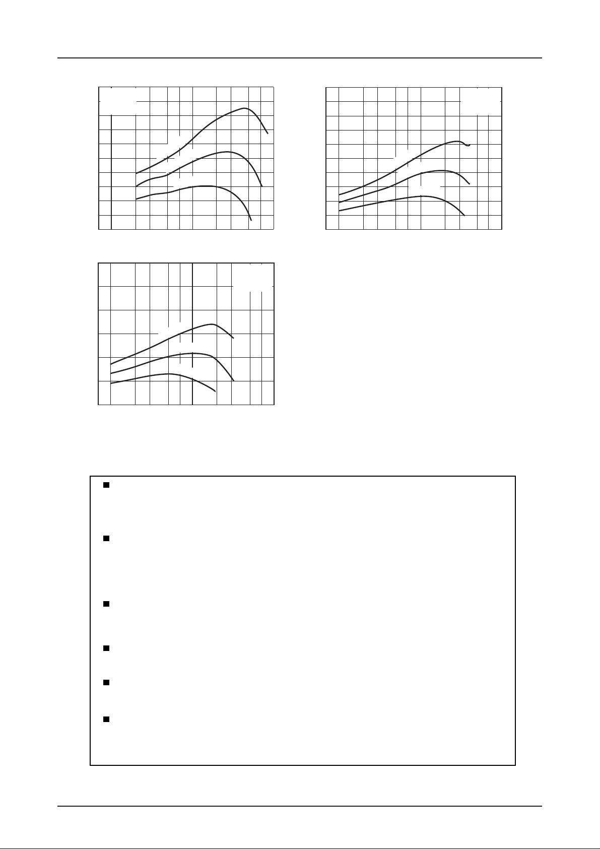
RL=3Ω
f=1kHz
9
Rg=600Ω
8
7
6
5
4
3
2
Power dissipation, Pd – W
1
0
0.17
Pd – P
=15V
CC
V
CC
V
Output power, Po – W
6
5
4
3
2
Power dissipation, Pd – W
1
Pd – P
CC
V
O
=12V
=9V
V
CC
1.0 10 1.0 102 3 57 2 3 57 57 2 3 57
10
9
8
7
6
5
4
3
2
Power dissipation, Pd – W
1
0
0.1723
Pd – P
CC
V
V
=15V
CC
V
=12V
CC
O
=9V
Output power, Po – W
O
RL=8Ω
f=1kHz
Rg=600Ω
=15V
=12V
V
CC
V
CC
=9V
RL=4Ω
f=1kHz
Rg=600Ω
0
7
0.1 2 3 57 2 3 57
101.0
Output power, Po – W
Specifications of any and all SANYO products described or contained herein stipulate the performance,
characteristics, and functions of the described products in the independent state, and are not guarantees
of the performance, characteristics, and functions of the described products as mounted in the customer's
products or equipment. To verify symptoms and states that cannot be evaluated in an independent device,
the customer should always evaluate and test devices mounted in the customer's products or equipment.
SANYO Electric Co., Ltd. strives to supply high-quality high-reliability products. However, any and all
semiconductor products fail with some probability. It is possible that these probabilistic failures could
give rise to accidents or events that could endanger human lives, that could give rise to smoke or fire,
or that could cause damage to other property. When designing equipment, adopt safety measures so
that these kinds of accidents or events cannot occur. Such measures include but are not limited to protective
circuits and error prevention circuits for safe design, redundant design, and structural design.
In the event that any or all SANYO products(including technical data,services) described or
contained herein are controlled under any of applicable local export control laws and regulations,
such products must not be exported without obtaining the export license from the authorities
concerned in accordance with the above law.
No part of this publication may be reproduced or transmitted in any form or by any means, electronic or
mechanical, including photocopying and recording, or any information storage or retrieval system,
or otherwise, without the prior written permission of SANYO Electric Co. , Ltd.
Any and all information described or contained herein are subject to change without notice due to
product/technology improvement, etc. When designing equipment, refer to the "Delivery Specification"
for the SANYO product that you intend to use.
Information (including circuit diagrams and circuit parameters) herein is for example only ; it is not
guaranteed for volume production. SANYO believes information herein is accurate and reliable, but
no guarantees are made or implied regarding its use or any infringements of intellectual property rights
or other rights of third parties.
This catalog provides information as of November, 1998. Specifications and information herein are subject to change
without notice.
No. 6012-7/7
PS
 Loading...