

Page 1
Ordering number: EN4022C
Monolithic Linear IC
LA4525
Dual AF Power Amplifier
for Radio Cassette Recorders
Overview
The LA4525 requires only a small number of external
components to drive either two 4 Ω speakers or one 8 Ω
speaker. The output power is typically 0.65 W when driving
two 4 Ω speakers.
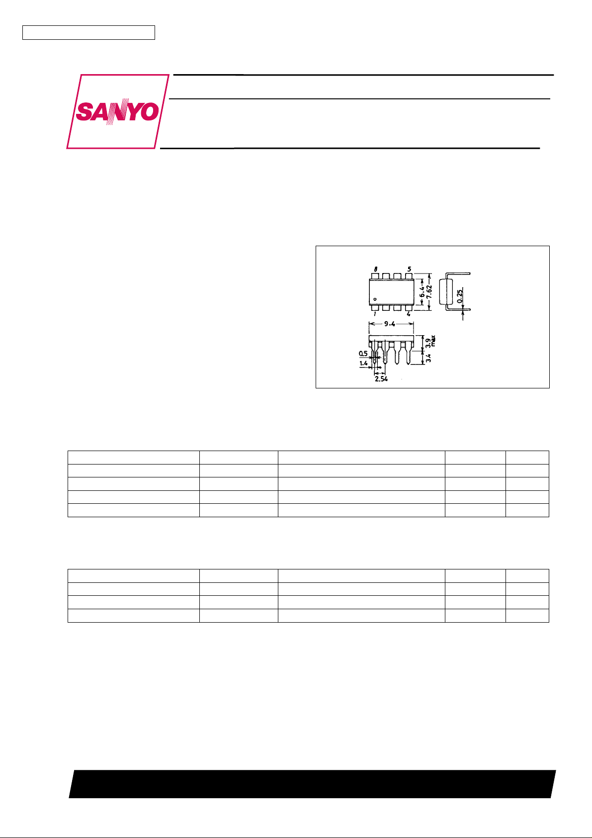
Package Dimensions
unit : mm
3001B-DIP8
[LA4525]
Features
.
Two-channel (dual) or single-channel (BTL) operation
.
Requires only a few external components.
.
0.65 W (typ) output power into two 4 Ω speakers
.
Wide power supply range: 3 to 15 V
.
8-pin DIP (No heat sink needed)
SANYO : DIP8
Specifications
Absolute Maximum Ratings at Ta = 25°C
Parameter Symbol Conditions Ratings Unit
Maximum supply voltage V
Allowable power dissipation Pd max Note 1.5 W
Operating temperature Topr –25 to +75 °C
Storage temperature Tstg –40 to +150 °C
max Rg = 0 15 V
CC
Note: Mounted on a 50 × 50 × 1.6 mm3heat dissipating board
Recommended Operating Conditions at Ta = 25°C
Parameter Symbol Conditions Ratings Unit
Supply voltage V
Load resistance range R
Supply voltage range V
CC
L
op Not in excess of package Pd 3 to 15 V
CC
SANYO Electric Co.,Ltd. Semiconductor Bussiness Headquarters
TOKYO OFFICE Tokyo Bldg., 1-10, 1 Chome, Ueno, Taito-ku, TOKYO, 110 JAPAN
32896HA(II)/D0192TS/4162TS No.4022-1/8
6V
4 Ω
Page 2
LA4525
Operating Characteristics at VCC= 6 V, Ta =25°C, RL=4Ω,f=1kHz, Rg = 600 Ω,
Dual operation unless otherwise noted
Parameter Symbol Condition min typ max Unit
Quiescent supply current I
Output power
CCO
P
O
P
O
Voltage gain VG V
Total harmonic distortion THD P
Output noise voltage V
NO
Supply voltage ripple rejection SVRR Rg = 0 Ω,f
Channel separation CH Sep V
Input resistance Ri 70 100 130 kΩ
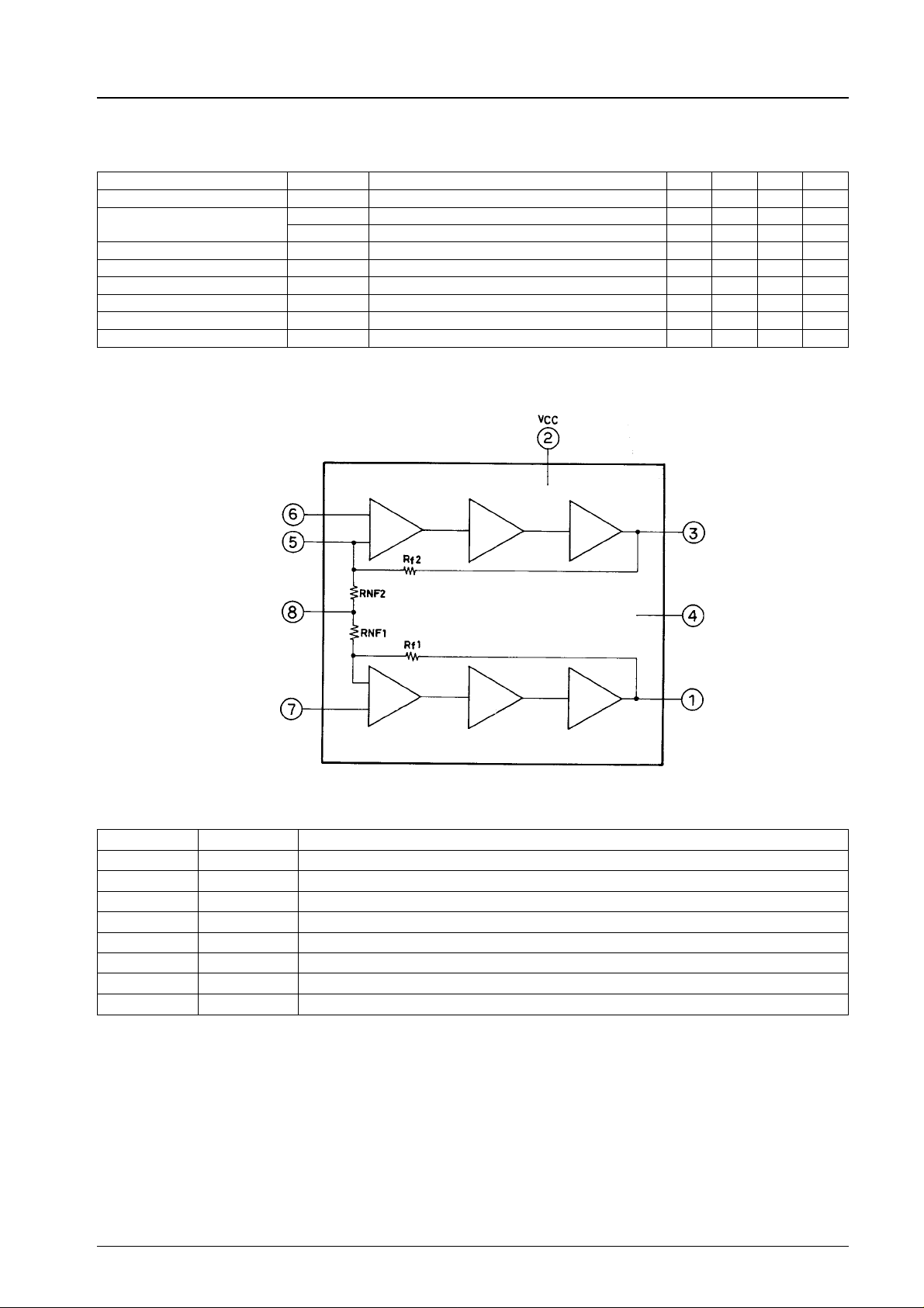
Equivalent Block Diagram
Rg=0Ω 10 15 30 mA
1 THD = 10% 0.45 0.65 W
2VCC=9V,RL=8Ω, THD = 10% 1.0 W
= 0 dBm 38 40 42 dB
O
= 0.1 W 0.2 0.7 %
O
Rg=0Ω, DIN AUDIO filter 100 400 µV
= 100 Hz, VR= 0 dBm 35 43 dB
R
= 0 dBm, Rg=0Ω 45 55 dB
O
IN2
BTL IN
Ch2
input
amp.
Predriver
amp.
PRE GND
IN1
Ch1
input
amp.
Predriver
amp.
Pin Description
Number Name Description
1 OUT1 Channel 1 output
2V
CC
3 OUT2 Channel 2 output
4 POWER GND Power amplifier ground
5 BTL IN Bridge test load input
6 IN2 Channel 2 input
7 IN1 Channel 1 input
8 PRE GND Preamplifier ground
Supply voltage
Output
amp.
Output
amp.
OUT2
POWER GND
OUT1
No.4022-2/8
Page 3
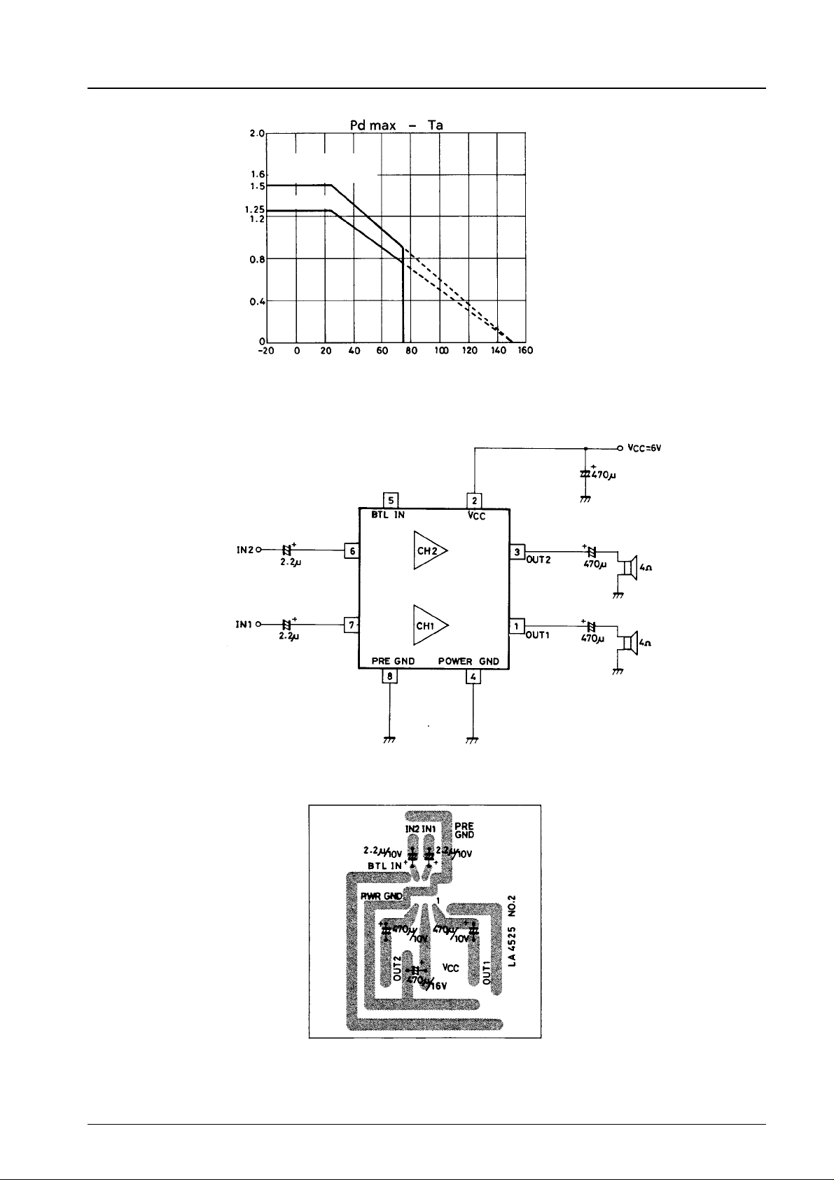
Dual Operation
Mounted on Sanyo
recommended board
Independent IC
Allowable power dissipation, Pd max − W
LA4525
Ambient temperature, Ta − °C
Sample Printed Circuit Pattern
Unit (capacitance:F)
Unit (capacitance:F)
65 × 65mm
2
(Cu-foiled area)
No.4022-3/8
Page 4
LA4525
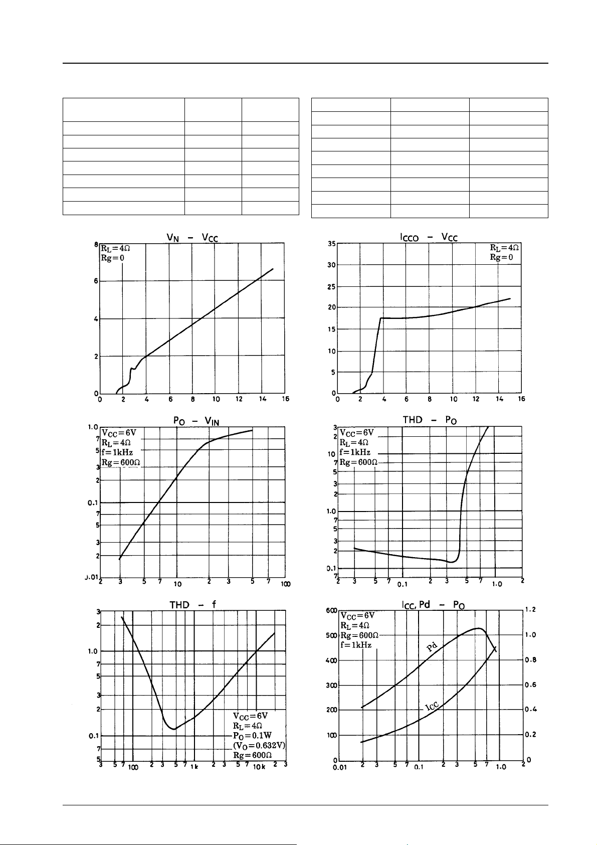
External Components Comparison
External components
Output capacitors ••
Input capacitors ••
Bootstrap capacitors • ×
Feedback capacitors • ×
Filter capacitors • ×
Oscillation damping mylars • ×
Dual-mode operation total 11 4
−V
N
Output pin voltage, V
Existing
Sanyo ICs
LA4525
Pin Voltages
Pin number Pin name Pin voltage
1 OUT1 2.8 V
2V
3 OUT2 2.8 V
4 POWER GND 0 V
5 BTL IN 65 mV
6 IN2 1.4 V
7 IN1 1.4 V
8 PRE GND 0 V
−mA
CCO
Quiescent current, I
CC
6V
−W
O
Output power, P
Supply voltage, VCC−V
Input voltage, VIN−mV
Supply voltage, VCC−V
Total harmonic distortion, THD − %
Output power, PO−W
−mA
CC
Current drain, I
Power dissipation, Pd − W
Total harmonic distortion, THD − %
Frequency,f−Hz
Output power, PO−W
No.4022-4/8
Page 5
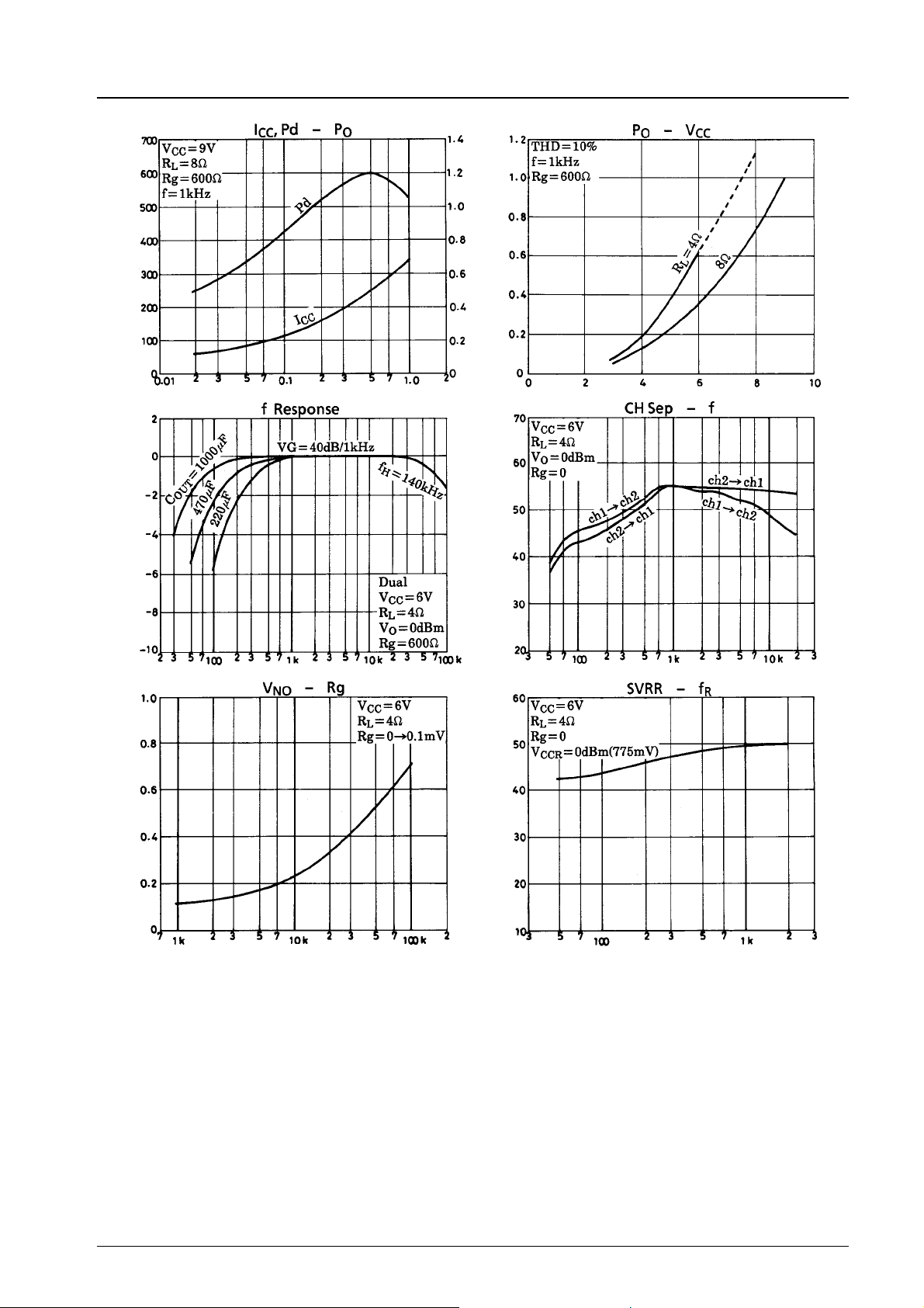
LA4525
−mA
Current drain, I
Frequency response − dB
CC
Output power, PO−W
−W
O
Output power, P
Power dissipation, Pd − W
Supply voltage, VCC−V
Channel separation, CH sep − dB
−mV
Output noise voltage, V
NO
Frequency,f−Hz
Signal source resistance, Rg − Ω
Frequency,f−Hz
Ripple rejection, SVRR − dB
Ripple frequency, fR−Hz
No.4022-5/8
Page 6
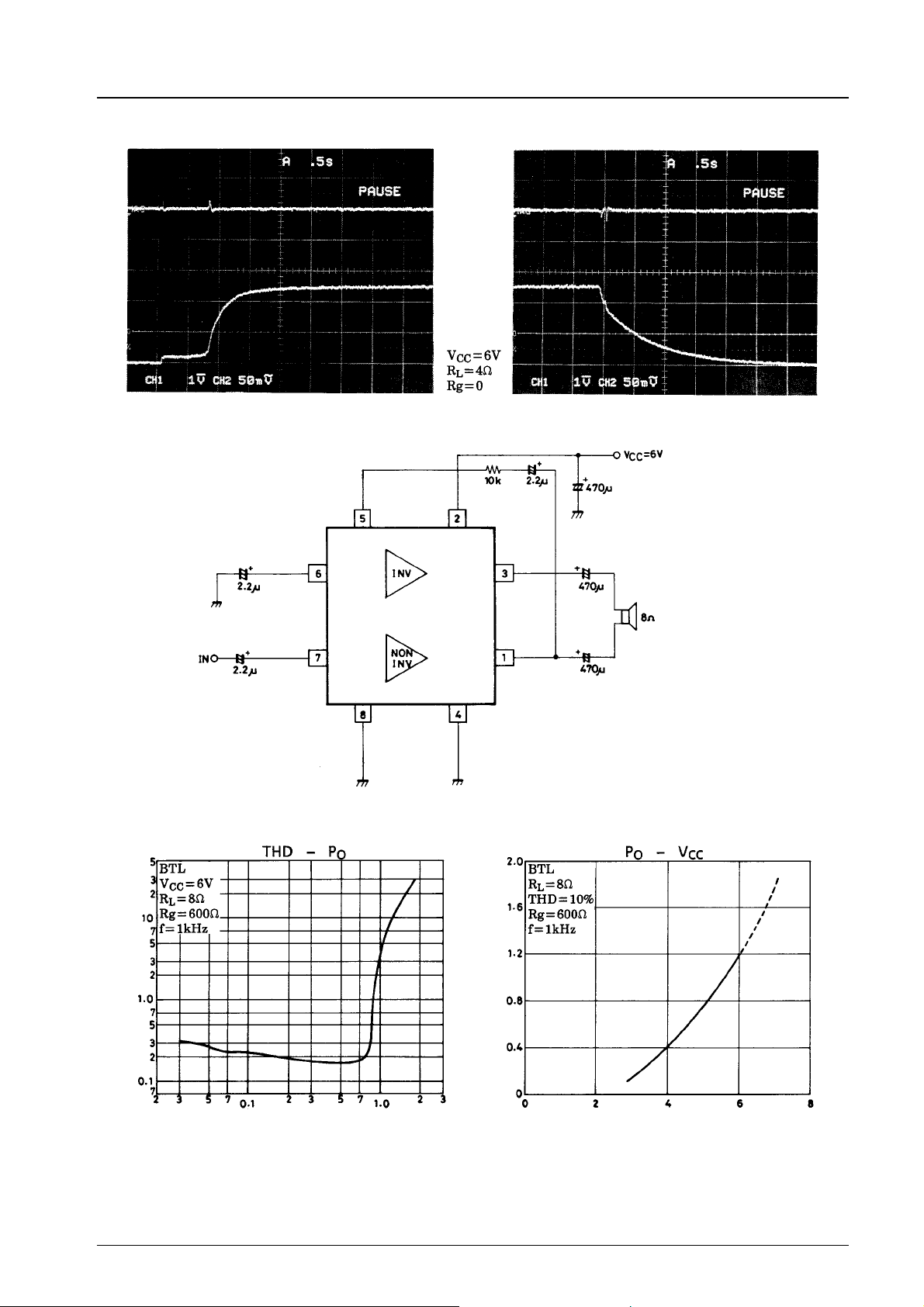
Rising and falling waveforms
BTL Operation
LA4525
Speaker
terminals
Output DC
locus
Unit (resistance: Ω, capacitance:F)
−W
O
Output power, P
Total harmonic distortion, THD − %
Output power, PO−W
Supply voltage, VCC−V
No.4022-6/8
Page 7
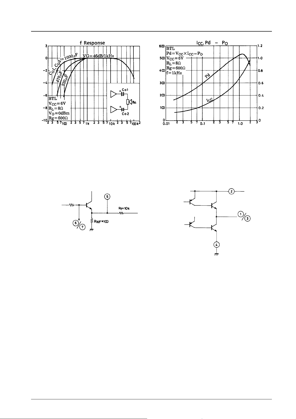
LA4525
−mA
CC
Frequency response − dB
Frequency,f−Hz
Handling Instructions and Precautions
Internal Circuits
Unit (resistance: Ω)
Figure 1. Input pins (6 and 7) and
BTL input pin (5)
Current drain, I
Output power, PO−W
Driver
Driver
Power
Power
Power dissipation, Pd − W
Figure 2. Output pins (1 and 3)
No.4022-7/8
Page 8
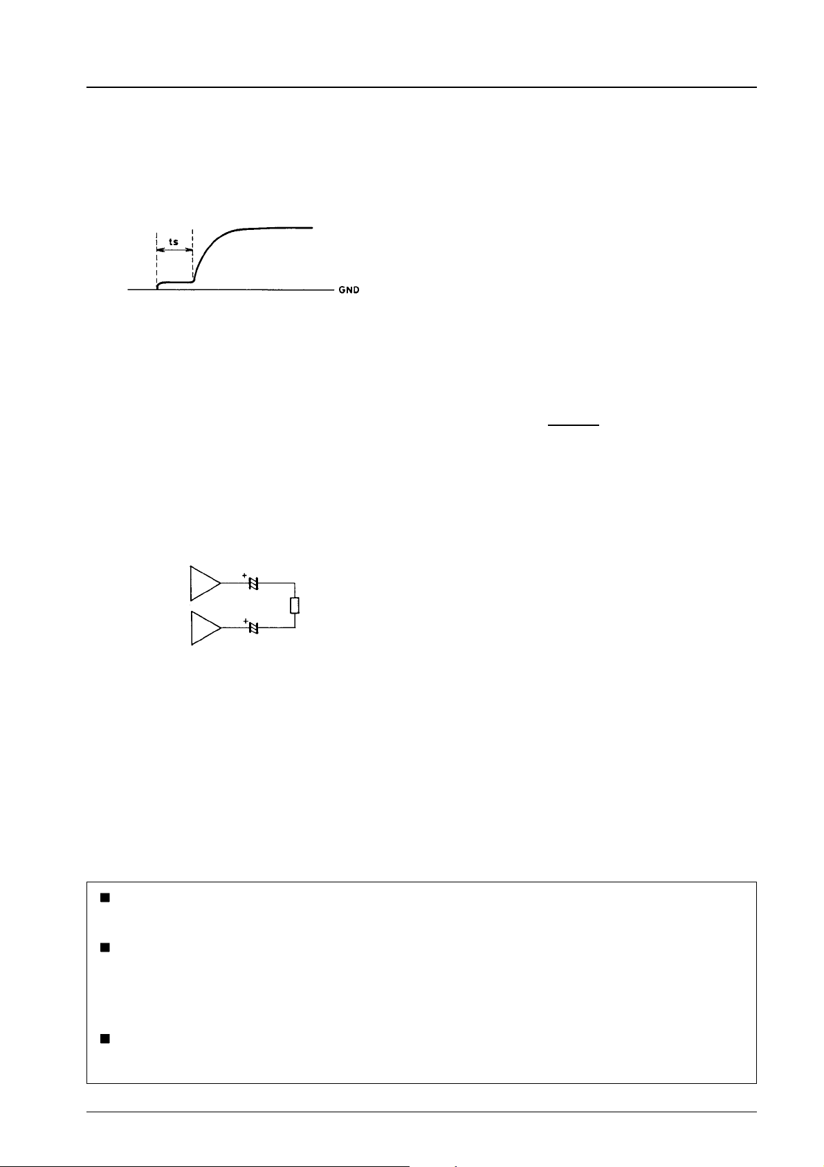
External Components
.
The starting time, ts, can be varied by changing the value of
the input capacitor. A value of 2.2 µF is recommended. A
smaller value will result in a lower starting time, and a larger
value, a higher starting time.
.
The output capacitor should have a value of 470 µF. A lower
value will cause the low-frequency roll-off and low-power
characteristics to deteriorate.
.
A value of 470 µF is recommended for the power supply
capacitor, although this can change according to the design
setup conditions.
.
In dual mode, BTL IN (the channel 2 negative feedback
connection) should be left floating.
BTL mode
.
The output capacitors should have a value of 470 µF. If these
are omitted, a ‘‘popping’’ noise occurs. Also, any output
offset will cause a current to flow which could damage the
load under quiescent DC conditions.
R
L
LA4525
.
The output capacitors can be replaced with a single 220 µF
bipolar capacitor. A larger value can cause switching noise
when power is applied to the device.
.
The voltage gain is fixed internally to 40 dB in dual mode
and 46 dB in BTL mode. These values cannot be altered by
connecting external components.
.
Phase correction capacitance (600 pF/TOTAL) is
incorporated in the internal stages. Oscillation damping
components (R and C) are also incorporated in the output pin
circuits.
.
Power consumption
Note that the 8-pin DIP does not have a heat dissipating
surface and that the power dissipation ratings are critical.
The maximum power dissipation of the device is 1.25 W,
and 1.5 W when the device is mounted on the recommended
PCB. The actual power dissipated depends on the supply
voltage and the load conditions. Ensure that the device is
kept within its maximum rating. For AC supplies,
transformer tappings may need to be adjusted to keep the
device within maximum ratings.
Pd max =
Note
For BTL mode operation, the value of R
calculation should be 1/2 the actual value.
.
If the speaker plug jacks short to ground when connected, a
protection resistor should be inserted in the output line.
.
If the device is operated at or near its rated values, these
values can be exceeded by small changes in operating
conditions, leading to device breakdown. Accordingly, ensure
that a safety margin is maintained so as not to exceed the
maximum ratings.
.
Check the PCB surface after soldering to ensure that no pins
have been accidentally shorted. Any short between pins could
cause poor operating characteristics or permanently damage
the device when power is applied.
.
If making the PCB, check the printed wiring to ensure that
no feedback loops occur between input and output.
V
π2R
CC
2
+I
× V
L
CCO
CC
used in the
L
No products described or contained herein are intended for use in surgical implants, life-support systems, aerospace equipment,
nuclear power control systems, vehicles, disaster/crime-prevention equipment and the like, the failure of which may directly or
indirectly cause injury, death or property loss.
Anyone purchasing any products described or contained herein for an above-mentioned use shall:
1 Accept full responsibility and indemnify and defend SANYO ELECTRIC CO., LTD., its affiliates, subsidiaries and distributors
and all their officers and employees, jointly and severally, against any and all claims and litigation and all damages, cost and
expenses associated with such use:
2 Not impose any responsibility for any fault or negligence which may be cited in any such claim or litigation on SANYO
ELECTRIC CO., LTD., its affiliates, subsidiaries and distributors or any of their officers and employees jointly or severally.
Information (including circuit diagrams and circuit parameters) herein is for example only; it is not guaranteed for volume
production. SANYO believes information hereinisaccurateand reliable, but no guarantees are made or implied regarding its use
or any infringements of intellectual property rights or other rights of third parties.
This catalog provides information as of March, 1996. Specifications and information herein are subject to change without notice.
No.4022-8/8
 Loading...