

Page 1
Ordering number: EN3309C
Monolithic Linear IC
LA4425A
5 W Power Amplifier with Very Few External Parts
for Car Radio and Car Stereo
Features
.
The world’s first power amplifier with very few external
parts.
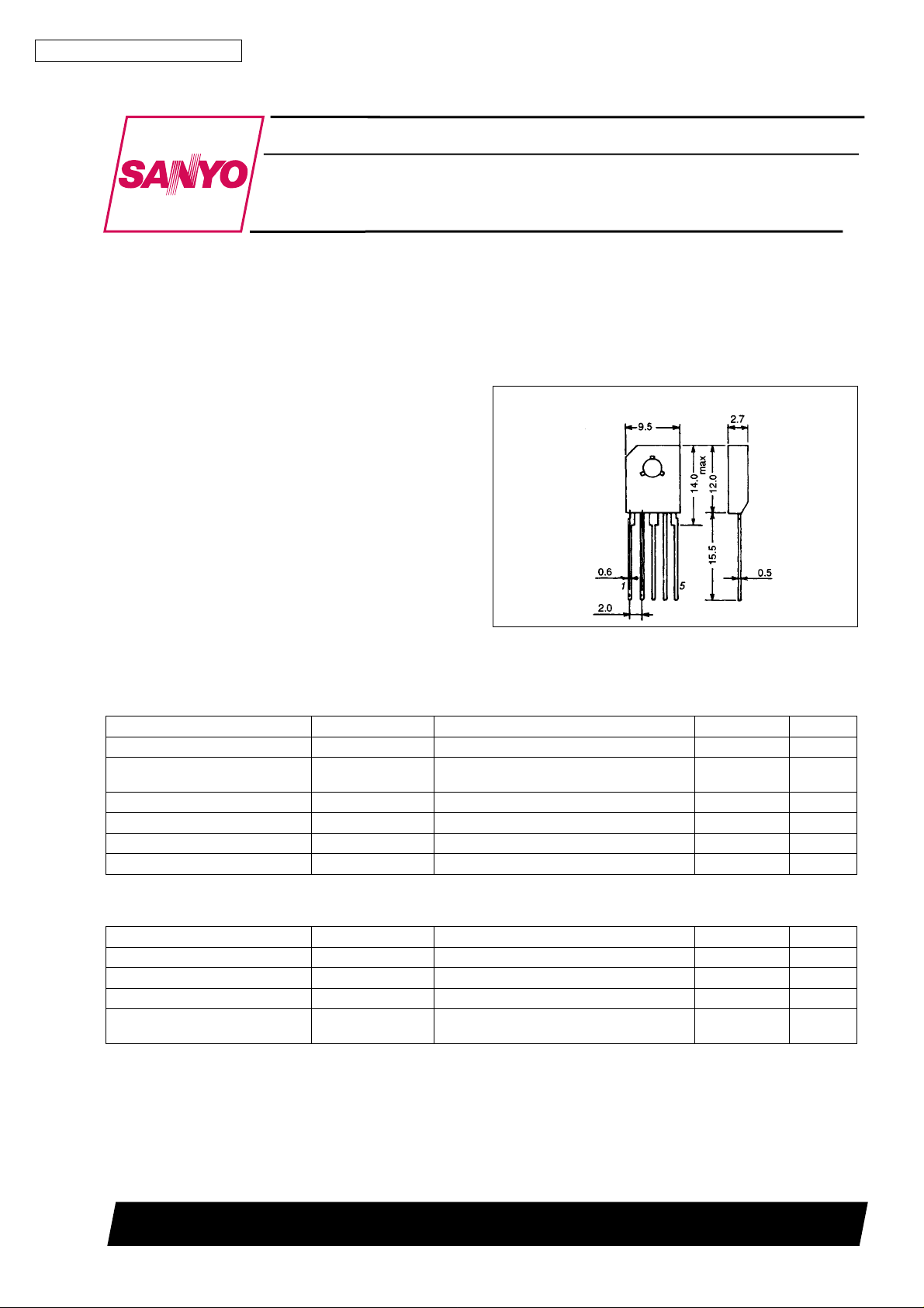
The smallest package in the industry
→ [SIP-5H (TO-126 type)]
Only two external parts
→ [Only I/O coupling capacitors]
.
Almost no evaluation, adjustment and check of its functions
as a power IC required
→ [Simplified control]
.
Wide operation supply range → 5to16V
.
On-chip protection:
Overvoltage protection
Thermal protection
Output D.C. short protection
.
On-chip pop noise reducing circuit
Package Dimensions
unit : mm
3031A-SIP-5H
[LA4425A]
SANYO : SIP5H
Specifications
Maximum Ratings at Ta = 25°C
Parameter Symbol Conditions Ratings Unit
Maximum supply voltage V
Surge maximum supply voltage V
Maximum output current I
Allowable power dissipation Pd max With infinite heat sink 7.5 W
Operating temperature Topr –30 to +80 °C
Storage temperature Tstg –40 to +150 °C
max Rg = 0 18 V
CC
surge
CC
peak 3.3 A
O
Giant pulse 200 msec
Rise time 1 ms
50 V
Operating Conditions at Ta = 25°C
Parameter Symbol Conditions Ratings Unit
Recommended supply voltage V
Recommended load resistance R
Operating voltage range V
Operating load resistance range R
CC
L
op 5to16 V
CC
op
L
Under conditions where maximum ratings
are not exceeded
SANYO Electric Co.,Ltd. Semiconductor Bussiness Headquarters
TOKYO OFFICE Tokyo Bldg., 1-10, 1 Chome, Ueno, Taito-ku, TOKYO, 110 JAPAN
53096HA(II)/20293TS/9200TA,TS(KOTO)/3050TA,TS(AF) No.3309-1/8
13.2 V
4 Ω
2to8 Ω
Page 2
LA4425A
Operating Characteristics at Ta = 25°C, VCC= 13.2 V, RL=4Ω,f=1kHz, Rg = 600 Ω, specified
3
board/specified circuit, 30 × 30 × 1.5 mm
Parameter Symbol Conditions min typ max Unit
Quiescent current I
Voltage gain VG V
Output power
Total harmonic distortion THD V
Output noise voltage V
Ripple rejection ratio
Overvoltage attack V
Starting time t
Input resistance R
Roll-off frequency
Thermal operating temperature Tc 125 °C
CCO
P
1 13.2 V/4 Ω, THD = 10% 4 5 W
O
P
2 14.4 V/4 Ω, THD = 10% 5 6 W
O
NO
SVRR
1
SVRR
2
CCX
s
IN
f
L
f
H
= 0 dBm 43 45 47 dB
O
= 2V 0.1 1.0 %
O
Rg = 0, BPF = 20 Hz to 20 kHz 0.15 0.5 mV
Rg=0,BPF=20Hzto20kHz
V
= 0 dBm, fR= 100 Hz
R
Rg=0,BPF=20Hzto20kHz
V
= 0 dBm, fR= 1 kHz
R
Rg = 0 21.5 V
thick aluminum used
65 130 mA
30 40 dB
47 dB
0.35 s
50 kΩ
40 Hz
90 kHz
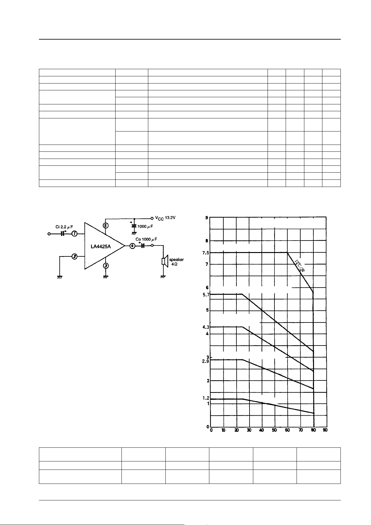
Sample Application Circuit
Pd max – Ta
With silicone grease applied.
Heat sink mounting torque 39 N·cm
.
On-chip overvoltage protection
.
On-chip thermal protection
.
On-chip pop noise reducing circuit
.
On-chip output D.C. short protection
With infinite heat sink
With 100 × 100 × 1.5 mm
With 50 × 50 × 1.5 mm
Al heat sink
With 30 × 30 × 1.5 mm
Allowable Power Dissipation, Pd max – W
3
Al heat sink
3
3
Al heat sink
No heat sink
Pin Voltage at VCC= 13.2 V
Characteristics Input
PinNo. 12345
Pin voltage
(reference value)
(6 2V
1.4 V
BE
Ambient temperature, Ta – °C
Small signal
GND
)
0V 0V
Large signal
GND
Output V
(6 1/2 VCC)
6.5 V
CC
(VCC)
13.2 V
No.3309-2/8
Page 3
LA4425A
IC Usage Notes
Maximum ratings
If the IC is used in the vicinity of the maximum ratings, even a slight variation in conditions may cause the maximum ratings to
be exceeded, thereby leading to a breakdown.
Printed circuit board
When drawing the printed circuit pattern, refer to the sample printed circuit pattern. Be careful not to form a feedback loop
between input and output.
Comparison of External Components
External Parts Our ICs now in use LA4425A
Output coupling capacitor jj
Input coupling capacitor jj
Bootstrap capacitor j —
Feedback capacitor j —
Filter capacitor j —
Phase compensation capacitor j —
Oscillation correction polyester
film capacitor
Oscillation correction resistor j —
Total 8 pcs. 2 pcs.
j —
Note: The power supply capacitor is not counted as a power IC part.
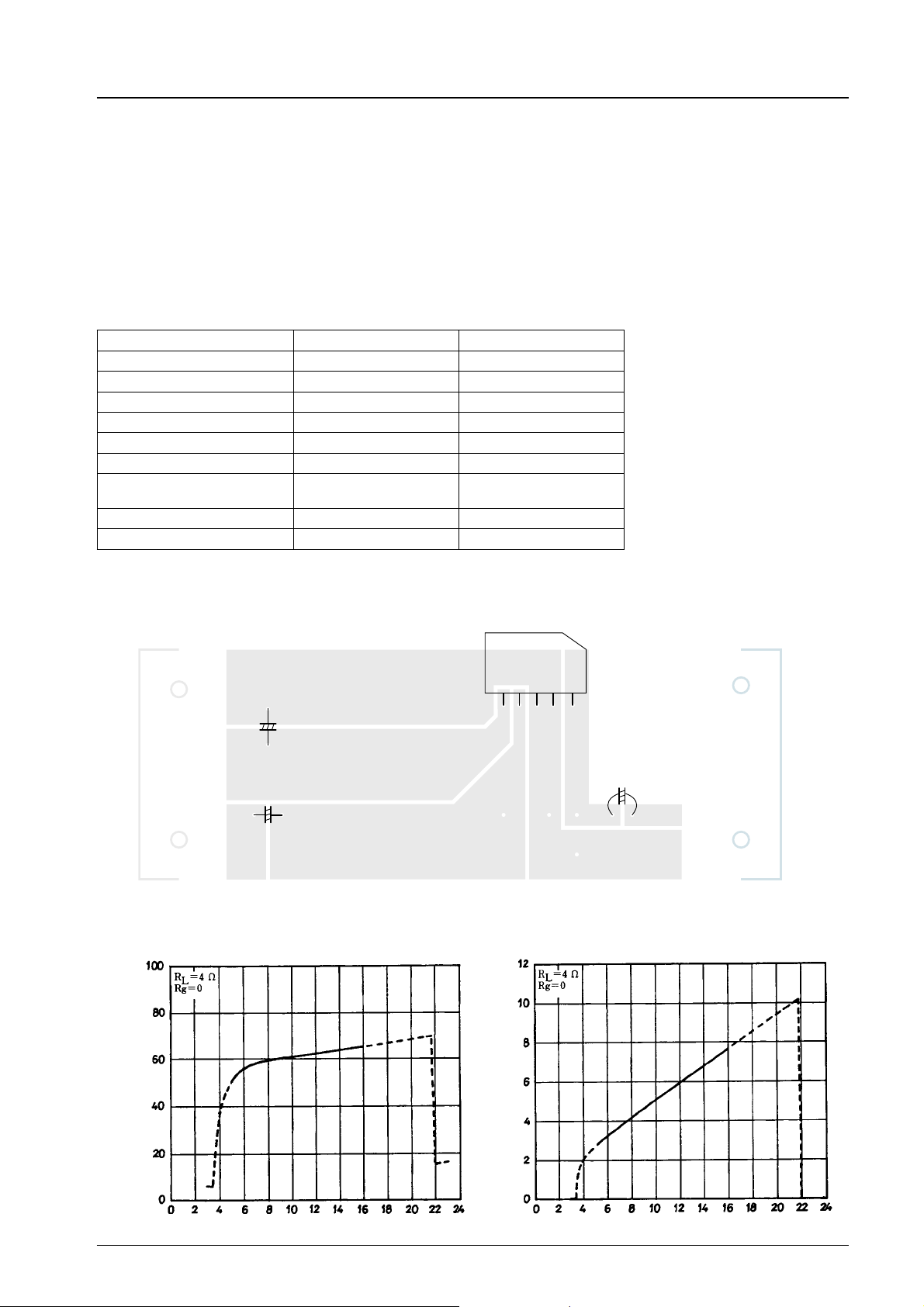
Sample Printed Circuit Pattern
–mA
CCO
GND
V
CC
OUT Co = 1000 µF
= 1000 µF
CV
CC
–
+
+–
I
CCO–VCC
LA4425A
+
–
Ci = 2.2 µF GND
Cu-foiled side 78.0 × 29.0 mm
VN–V
–V
N
IN
2
CC
Quiescent current, I
Supply voltage, VCC–V
Output pin voltage, V
Supply voltage, VCC–V
No.3309-3/8
Page 4
LA4425A
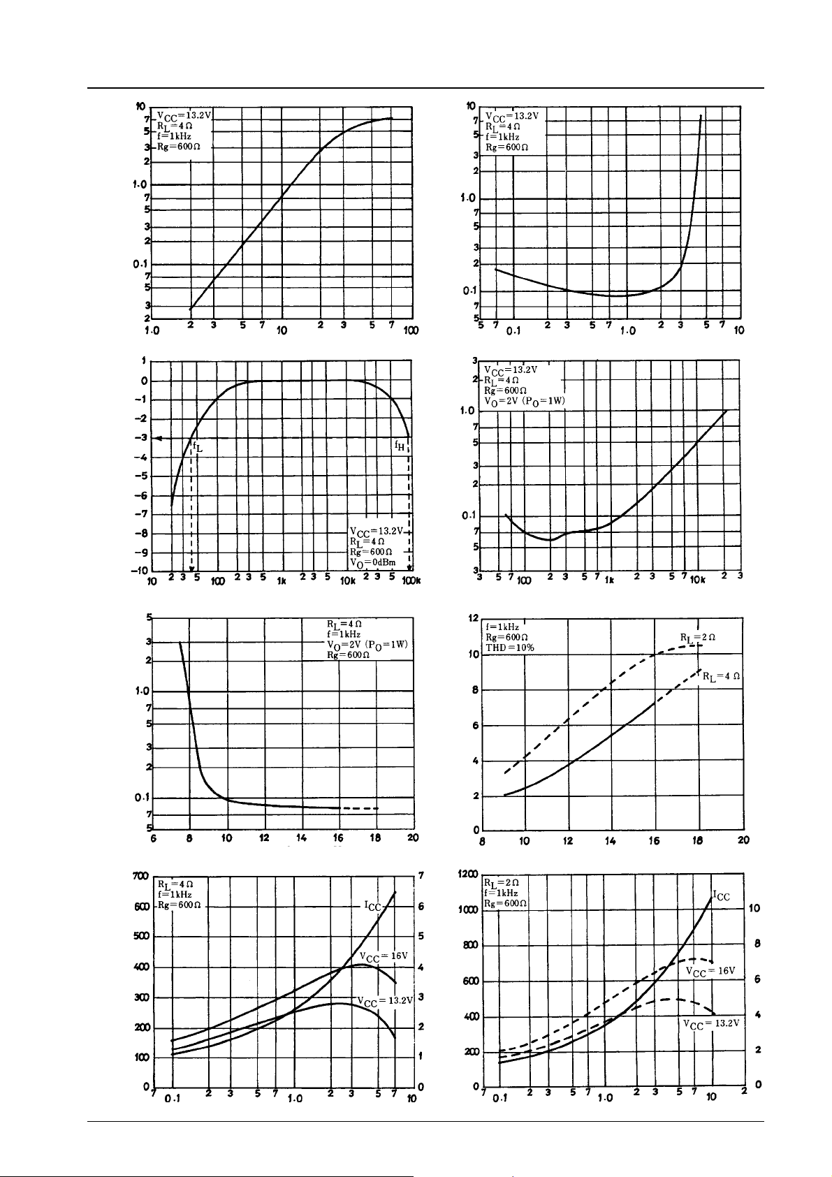
–W
O
Ouput power, P
PO–V
IN
Input voltage, VIN–mV
f Response
THD–P
O
Total harmonic distortion, THD – %
Output power, PO–W
THD–f
Response – dB
Total harmonic distortion, THD – %
Frequency,f–Hz
THD–V
CC
Frequency,f–Hz
PO–V
CC
–W
O
Output power, P
Total harmonic distortion, THD – %
Supply voltage, VCC–V
ICC,Pd–P
O
Supply voltage, VCC–V
ICC,Pd–P
O
–mA
Current drain, I
CC
Output power, PO–W
Power dissipation, Pd – W
–mA
Current drain, I
CC
Power dissipation, Pd – W
Output power, PO–W
No.3309-4/8
Page 5
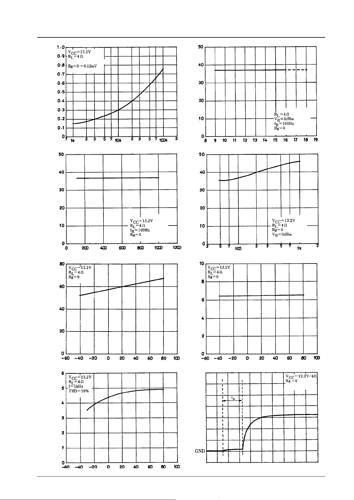
LA4425A
BPF=20Hzto20kHz
–mV
NO
Output noise voltage , V
VNO–Rg
Signal source resistance, Rg – Ω
SVRR – V
R
SVRR – V
Ripple rejection ratio, SVRR – dB
CC
BPF=20Hzto20kHz
Supply voltage, VCC–V
SVRR – fR
Ripple rejection ratio, SVRR – dB
–mA
CCO
Quiescent current, I
–W
O
BPF=20Hzto20kHz
Power supply ripple, VR– mVrms
I
–Ta
CCO
Ambient temperature, Ta – °C
PO–Ta
Ripple rejection ratio, SVRR – dB
–V
N
Output pin voltage, V
BPF=20Hzto20kHz
Ripple frequency, fR–Hz
VN–Ta
Ambient temperature, Ta – °C
Switch ‘‘ON’’ locus
2 V/div
Output power, P
Ambient temperature, Ta – °C
0.2 s/div
No.3309-5/8
Page 6
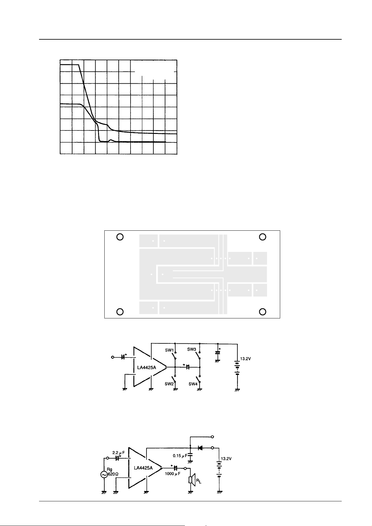
LA4425A
VCC= 13.2 V/4 Ω
Rg=0
‘‘OFF’’ locus
2 V/div
GND
0.2 s/div
Instructions and Precautions
.
Connect a capacitor of 1000 pF across pins 1 and 2 for external disturbance path.
.
Be careful of the ground line artwork when laying out the printed circuit pattern. Arrange so that the Sg route and load current
flow-in route do not overlap. Refer to the recommended printed circuit pattern or make slits, etc. at pins 2 and 3.
DUAL Printed Circuit Pattern Example
OUT1
V
CC
OUT2
.
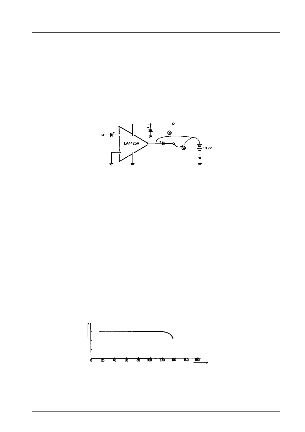
Short Circuit Tests
GND
1
IN1
GND
IN2
1
Cu-foiled side 45.0 × 75.0 mm
2
Sanyo’s recommended printed circuit board: Apply V
be protected from the DC/AC shorting of switches 1 to 4 above. However, be careful not to damage the IC by turning V
when DC short (SW 1 or SW 2) is on.
.
Power Supply Positive Surge
= 13.2 V using a 30 × 30 × 1.5 mm3thick aluminum board. The IC will
CC
JASO tester
Application of giant pulse
No.3309-6/8
CC
‘‘ON’’
Page 7
LA4425A
The overvoltage protector (V
stage elements, in order to increase the power line’s capability of handling positive surge. This means, of course, that a V
(V
) type output stage element is used instead of the V
CBO
.
Load Resistance and Misoperation
It should be noted that when R
10 %), the ground detector (current × voltage Schmitt circuit) operates momentarily.
.
Precautions on TaB
If power voltage is applied to the IC substrate (the heat sink on a set), the IC structure is such that the PN junctions may be
burned, causing deterioration or destruction. Consult Sanyo’s Quality Assurance Department with regard to the energy handling
capability (voltage peak value, pulse width). Also, the IC TaB (substrate) is connected to pin 3, large signal GND.
.
Test of +VCCto Output Pin
The power pin is in a floating state when a power capacitor is connected, so if +V
power transistor inside the IC will be damaged.
The LA4425A has a protective bypass route inside the IC.
.
Starting Time (ts)
This is set at 0.35 sec/typ, but it can be made shorter by making input capacitor Ci smaller, or longer by making it larger.
.
Pop noise
The pop noise prevention circuit operates to reduce pop until Rg reaches 50 kΩ. However, if Rg is left open, the charging route
of input capacitor Ci is lost, so the pop noise reduction circuit stops operating and click noises become louder.
.
VG/OSC
The voltage gain is fixed at 45 dB inside the IC. It is impossible to change it externally.
Phase compensation capacitors (350 pF/total) are connected between individual stages inside the IC, and the open loop gain is
low. In addition, the upper and lower drives are made equivalent so that final stage current gain is adjusted, providing a measure
against unwanted high-frequency parasitic oscillation peculiar to power IC’s.
.
BTL Connection
Connection is impossible with IC alone.
.
Reverse Mounting of IC
The pin assignment is such that there is no danger of damage.
.
T.S.D (Thermal Shutdown) Operating Temperature
6 21.5 V) inside the IC is used to cut all bias routes and reverse bias between B-E of output
CCX
CEO(VCER
< 2 Ω and VCCis high, and the switch is turned ‘‘ON’’ when setting is for a signal (THD =
L
) type.
Floating
CC
touches output lines a and b, the upper
CES
O
,P
CC
I
30 × 30 × 1.5 mm3thick Al board
Ta = 25°C
TC(°C)
No.3309-7/8
Page 8

LA4425A
T.S.D is capable of starting operation at Tc 120 to 130°C. When this is converted to junction temperature (Tj) according to the
formula below.
Tj 6 165°C,
Tj = QjcvPd + Tc
As T.S.D operation progresses, the output pin bias voltage drops, and it becomes harder to drive the upper waveform. Therefore,
the current (I
Proper Cares in Mounting Radiator Fin
1. The mounting torque is in the range of 39 to 59 Nvcm.
2. The distance between screw holes of the radiator fin must coincide with the distance between screw holes of the IC.
3. The screw to be used must have a head equivalent to the one of truss machine screw or binder machine screw defined by JIS.
Washers must be also used to protect the IC case.
4. No foreign matter such as cutting particles shall exist between heat sink and radiator fin. When applying grease on the
junction surface, it must be applied uniformly on the whole surface.
5. Because the heatsink mounting tab and the heatsink are at the same electric potential as the chip’s GND, care must be taken
when mounting the heatsink on more than one device.
6. IC lead pins are soldered to the printed circuit board after the radiator fin is mounted on the IC.
) and power (PO) show a tendency to decrease.
CC
No products described or contained herein areintendedforuse in surgical implants, life-support systems, aerospace equipment,
nuclear power control systems, vehicles, disaster/crime-prevention equipment and the like, the failure of which may directly or
indirectly cause injury, death or property loss.
Anyone purchasing any products described or contained herein for an above-mentioned use shall:
1 Accept full responsibility and indemnify and defend SANYO ELECTRIC CO., LTD., its affiliates, subsidiaries and distributors
and all their officers and employees, jointly and severally, against any and all claims and litigation and all damages, cost and
expenses associated with such use:
2 Not impose any responsibility for any fault or negligence which may be cited in any such claim or litigation on SANYO
ELECTRIC CO., LTD., its affiliates, subsidiaries and distributors or any of their officers and employees jointly or severally.
Information (including circuit diagrams and circuit parameters) herein is for example only; it is not guaranteed for volume
production. SANYO believes information herein is accurate and reliable, but no guarantees are made or implied regarding its use
or any infringements of intellectual property rights or other rights of third parties.
This catalog provides information as of June, 1996 . Specifications and information herein are subject to change without notice.
No.3309-8/8
 Loading...