

Page 1
Any and all SANYO products described or contained herein do not have specifications that can handle
applications that require extremely high levels of reliability, such as life-support systems, aircraft’s
control systems, or other applications whose failure can be reasonably expected to result in serious
physical and/or material damage. Consult with your SANYO representative nearest you before using
any SANYO products described or contained herein in such applications.
SANYO assumes no responsibility for equipment failures that result from using products at values that
exceed, even momentarily, rated values (such as maximum ratings, operating condition ranges,or other
parameters) listed in products specifications of any and all SANYO products described or contained
herein.
Monolithic Linear IC
5V CD Headphone-stereo Power Amplifier
Ordering number:ENN4033A
LA4536M
SANYO Electric Co.,Ltd. Semiconductor Company
TOKYO OFFICE Tokyo Bldg., 1-10, 1 Chome, Ueno, Taito-ku, TOKYO, 110-8534 JAPAN
The LA4536M is a low noise, low distortion headphonestereo power IC designed for use on a portable CD.
Features
• Less current drain.
• Accept 16Ω load drive.
• Excellent voltage reduction characteristic.
• Excellent ripple rejection.
• Power switch function and built-in muting circuit.
• Low noise (7µV), low gain (11dB).
Specifications
Absolute Maximum Ratings at Ta = 25˚C
retemaraPlobmySsnoitidnoCsgnitaRtinU
egatlovylppusmumixaMV
noitapissidrewopelbawollAxamdP 003Wm
erutarepmetgnitarepOrpoT 57+ot02–
erutarepmetegarotSgtsT 521+ot04–
xamlangisoN 0.6V
CC
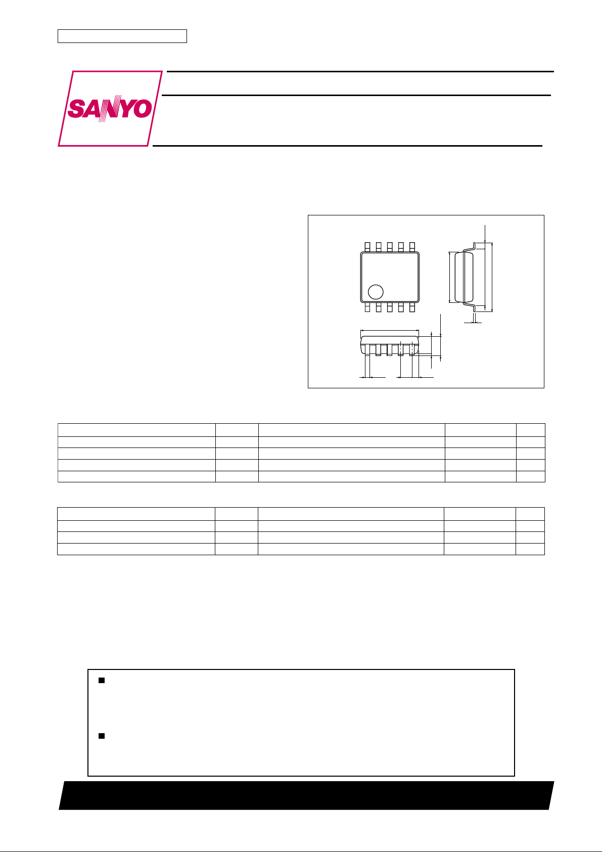
Package Dimensions
unit:mm
3086A-MFP10S
[LA4536M]
10
1
6
5
5.1
0.55
1.00.35
1.5˚
0.1
1.8max
4.4
0.15
SANYO : MFP10S
0.625
5.15
6.4
˚C
˚C
Operating Characteristics at Ta = 25˚C
retemaraPlobmySsnoitidnoCsgnitaRtinU
egatlovylppusdednemmoceRV
egnaregatlovylppusgnitarepOV
ecnadepmidaoldednemmoceRR
CC
poCC
L
O3098HA (KT)/62598RM (KI) No.4033–1/9
0.5V
0.6ot0.4V
23ot61 Ω
Page 2
LA4536M
Operating Characteristics at Ta = 25˚C, RL=16Ω, Rg=600Ω
retemaraPlobmySsnoitidnoC
I
1V
tnerructnecseiuQ
niagegatloVGVV
snoitairavniagegatloV
noitrotsidcinomrahlatoTDHTV
rewoptuptuOP
klatssorCTC
noitcejerelppRRRVS
egatlovesiontuptuOV
tceffefforewoPV
tceffeetuMV
ytivitisnestnerrucnorewoP1I
ytivitisnesegatlovfforewoP)ffo(1V5.06.0V
ytivitisnestnerrucffoetuM)ffo(01I2.00.2Aµ
ytivitisnesegatlovnoetuM)no(01V5.056.0V
I
I
∆VG1
∆VG2
OCC
OCC
OCC
O
ON
CC
2V
CC
3V
CC
CC
V
CC
V
CC
CC
V
CC
V
CC
V
O
V
CC
V
O
V
CC
V
CC
)ffo(O
V
NI
V
CC
)TM(O
V
NI
VCC=5.0V, V5≥0.85V
)no(
VCC=5.0V, V5≤0.1V
VCC=5.0V, V5 ≥0.85V
VCC=5.0V, V5≤0.1V
langison,V0.5=0.102Am
DNG,01nip,V0.6=1.10.4Am
DNG,1nip,V0.6=0.1Aµ
V,zHk1=f,V0.5=
V,zHk1=f,V0.5=
V,zHk1=f,V0.4=
P,zHk1=f,V0.5=
mBd01–=
k1=gR,V0.6= Ω,
zH02otzH02=FPB
mBd01–=
mBd01–=
mBd01–=91131Bd
O
mBd01–=0.1Bd
O
mBd02–=0.1Bd
O
Wm1=20.042.0%
O
%01=DHT,zHk1=f,V0.5=04001Wm
k1=gR,zHk1=f,V0.5= Ω,
k1=gR,zH001=f,V0.4= Ω,
zH001=FPB,mBd02–=
,DNGot1niP,zH001=f,V0.4=
,DNGot1niP,zH001=f,V0.4=
nimpytxam
0406Bd
5456Bd
*1 : Quiescent current is the current flowing into pin 6. The current flowing into pin 1 and pin 10 is at the maximum value and calculated from
the equation (V pin–0.5V)/16[V/kΩ], increasing total current.
sgnitaR
702Vµ
08– mBd
08– mBd
50.00.2Aµ
tinUetoN
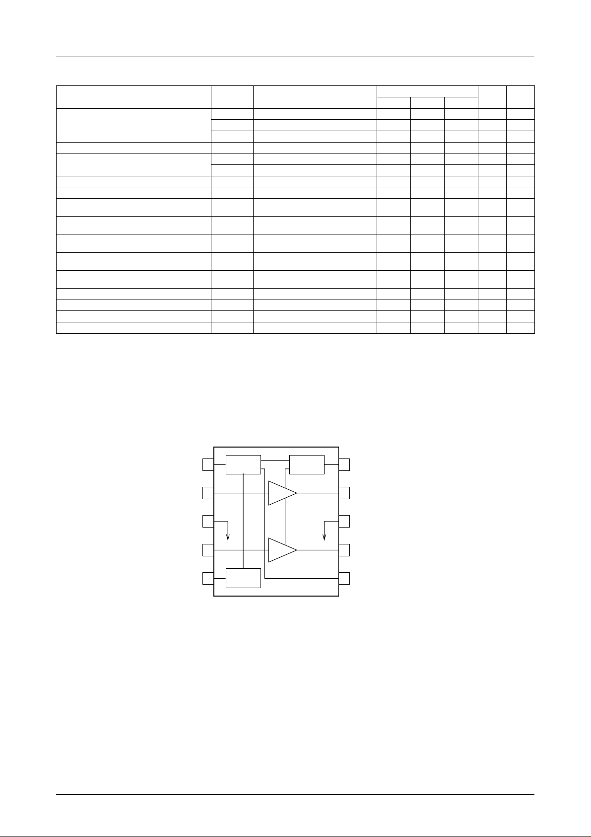
Equivalent Circuit Block Diagram
P/SW
IN 1
PRE GND
IN 2
REF
POWER
1
SWITCH
2
3
4
5
BIAS
Amp1
Amp2
MUTE
CIRCUIT
10
MT/SW
9
OUT 1
POWER GND
8
OUT 2
7
6
V
CC
A11160
No.4033–2/9
Page 3
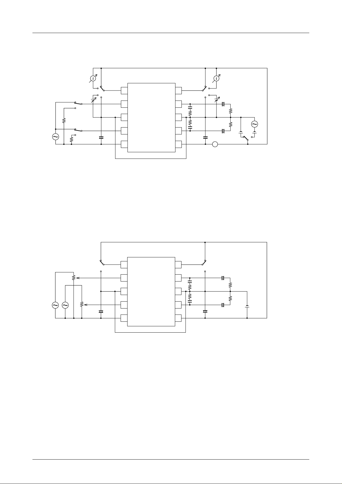
Test Circuit
LA4536M
I
1
2
3
V
1
1
2
Rg
1kΩ
1
2
SG
22µF 4.7µF
Rg
1kΩ
+
Sample Application Circuit
1
P/SW MT/SW
4
P/SW
1
IN 1
2
PRE
GND
IN 2
REF
LA4536M
3
4
5
MT/SW
OUT 1
POWER
GND
OUT 2
V
CC
10
9
8
7
6
0.1µF
2.2Ω
2.2Ω
0.1µF
I
10
1
2
3
V
4
+
10
220µF
+
R
L
16Ω
R
L
16Ω
+
220µF
A
I
CC
V
V
CC
DC RIPPLE
R
A11161
SG
0.1µF
2.2Ω
2.2Ω
0.1µF
OFF
ON
+
+
+
220µF
220µF
R
16Ω
R
16Ω
L
L
–
V
CC
+
A11162
ON
P/SW MT/SW
OFF
V
R
V
R
SG
1
2
22µF 4.7µF
+
P/SW
1
IN 1
2
PRE
LA4536M
3
GND
4
IN 2
5
REF
MT/SW
OUT 1
POWER
GND
OUT 2
V
CC
10
9
8
7
6
No.4033–3/9
Page 4
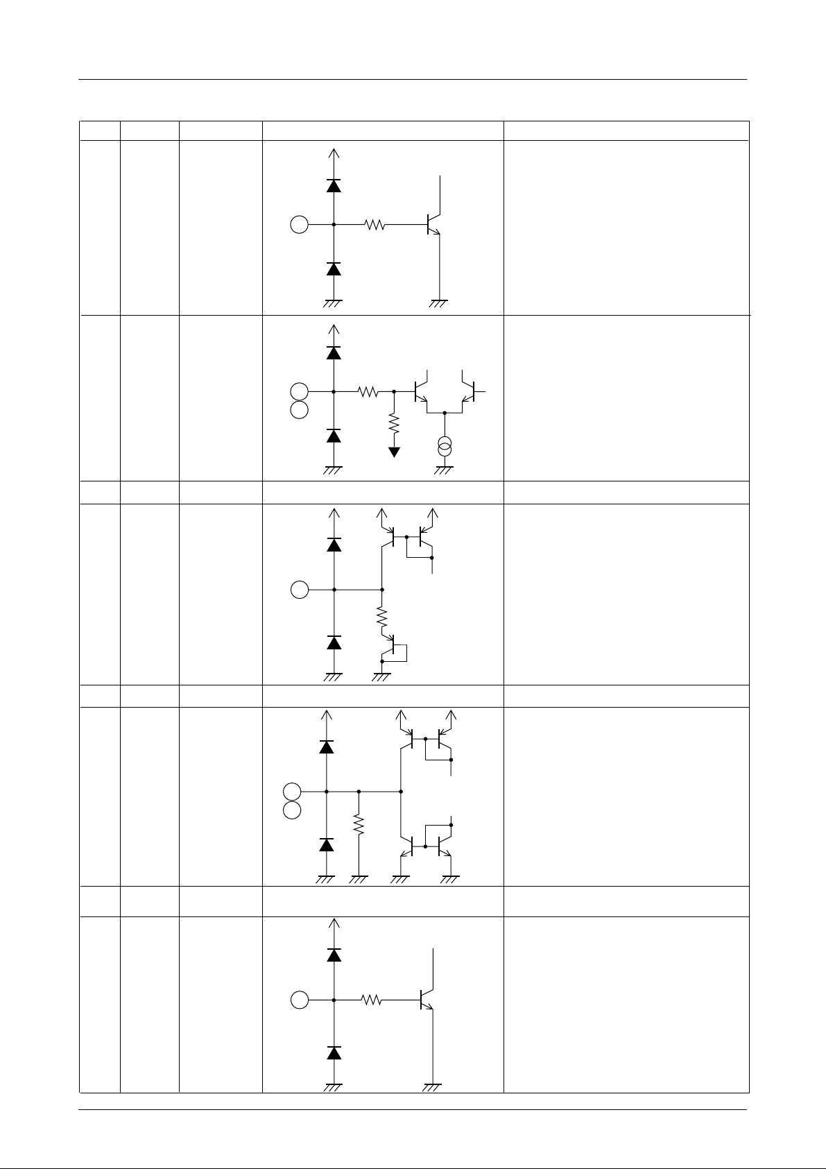
Pin Functions (VCC=5.0V)
LA4536M
Pin No.
1
2
4
3
Symbol Pin voltage Equivalent circuit Pin function
• The system runs on when the VCC is applied to this
pin and turns off by connectiong this pin to GND.
P/SW1
IN1
IN2
PRE GND
2.1
2.1
1
2
4
20kΩ
A11164
• Input pin connection.
Input impedance is 10kΩ.
500Ω
10kΩ
A11165
• 2.1V fixed bias is applied to this pin.
5
6
7
9
REF
V
CC
OUT2
OUT1
2.1
2.1
2.1
5
23kΩ
A11166
• Output pin connection.
7
9
4.7kΩ
A11167
POWER
8
GND
• The muting function turns on when this pin is
connected to GND and turns off by applying the V
to this pin.
CC
10
MT/SW
10
20kΩ
A11168
No.4033–4/9
Page 5
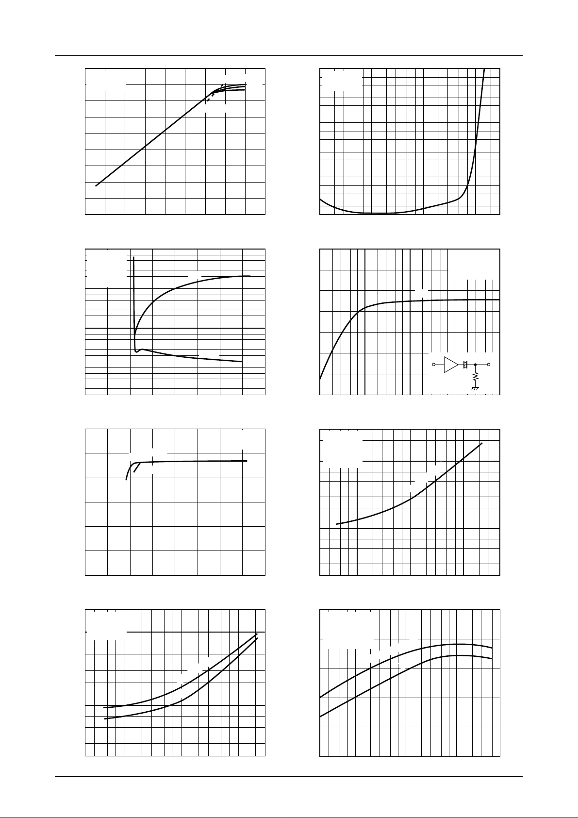
20
f=1kHz
RL=16Ω
10
0
—10
—20
– dBmOutput power, P
O
—30
—40
Output, V
—50
—60
—70
—60 —50 —40 —30 —20 —10 0 10 20—70
1000
7
f=1kHz
5
RL=16Ω
3
THD=10%
2
PO=1mW
100
7
5
– mW
3
O
2
10
7
5
3
2
1.0
7
5
3
2
0
12
160
140
120
100
VO – V
IN
THD=10%
Input voltage, VIN – dBm
PO,THD – V
CC
P
O
THD
3456
Power supply voltage, VCC – V
=–20dBm
V
O
VG – V
CC
–10dBm
V
CC
4.0V
f=1kHz
RL=16Ω
LA4536M
=6.0V
5.0V
10
7
5
3
2
1.0
7
5
3
2
0.1
7
5
3
2
0.01
7
5
3
2
10
VCC=5.0V
7
RL=16Ω
5
3
2
1.0
7
5
3
2
0.1
7
5
Total harmonic distortion, THD – %
3
2
23 57
0.1 1.0
THD – P
23 571023 2357
Output power, PO – mW
16
14
12
10
8
6
Voltage gain, VG – dBCurrent drain, I
Total harmonic distortion, THD – %
4
2
2
357
10 100
VG – f
23 57
Frequency, fIN – Hz
3
2
100
7
5
– mA
CC
3
2
VCC=5.0V
f=1kHz
RL=16Ω
2 output on
ICC – P
VG
1k
THD
O
IN
23 57
O
=10%
100
VCC=4.0V
VO=–10dBm
RL=16Ω
+
220µF
16Ω
23 5778
10k
OUT
100k
80
Voltage gain, VG – dB
60
40
210
34 5678
Power supply voltage, VCC – V
2
f=1kHz
RL=16Ω
1000
2 output on
7
5
3
2
100
7
5
Power dissipation, Pd – m W
3
2
23 57
1.0
Pd – P
23 571023 2357
Output power, PO – mW
CC
V
5.0V
O
=6.0V
100
10
7
5
3
2
3357
22 2
1.0 10
57 3 325 57
100
Output power, PO – mW
100
VCC=4.0V
CT – f
IN
RL=16Ω
Rg=1kΩ
80
VO=–10dBm
60
40
C
REF
=100µF
22µF
Crosstalk, CT – dB
20
0
2357
23571k2 3 57 23 57
100
Frequency, fIN – Hz
10k
No.4033–5/9
Page 6
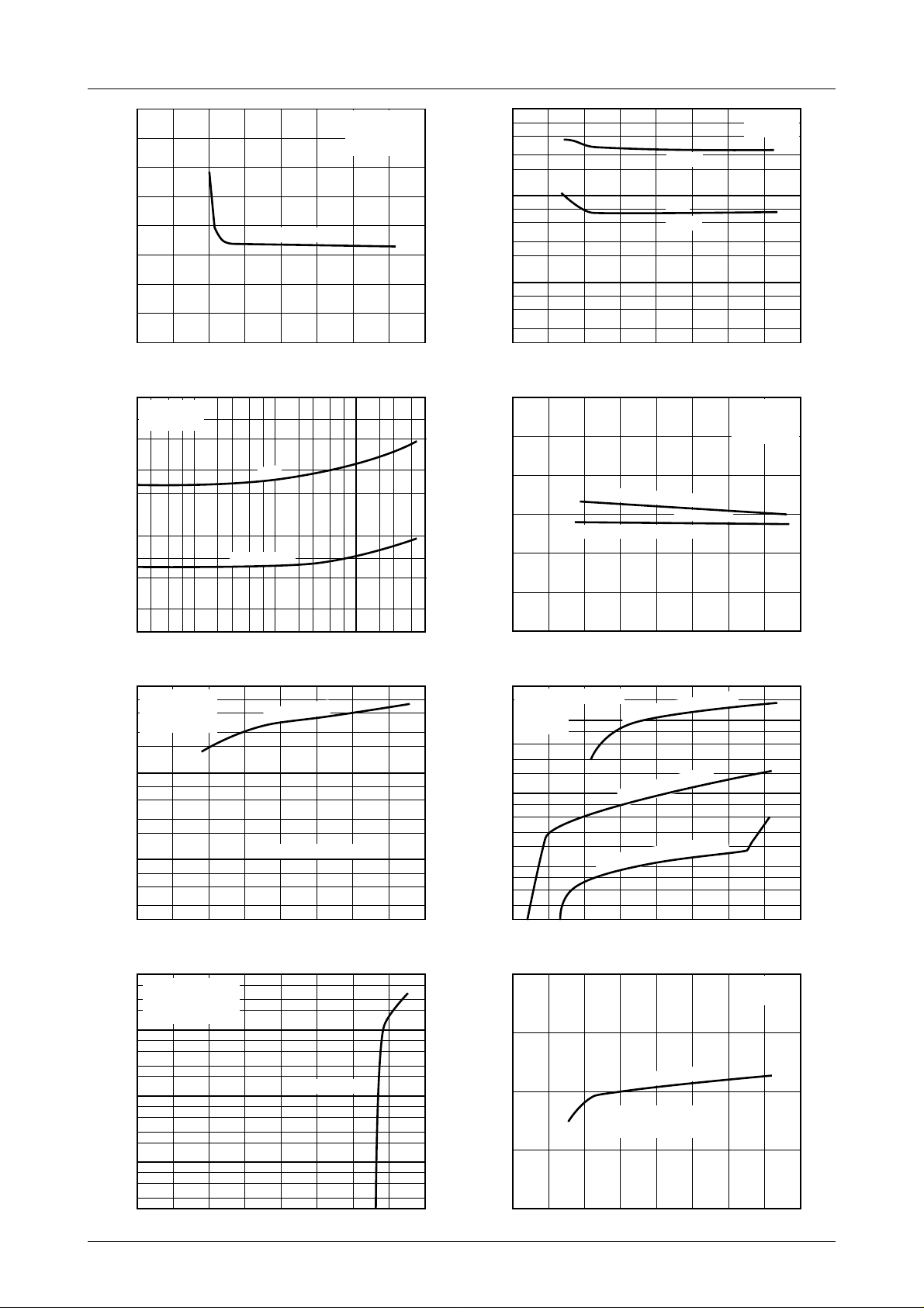
LA4536M
—20
—30
—40
—50
—60
—70
—80
Ripple rejection, SVRR – dBmOutput noise voltage, V
—90
—100
1
0
23 67 845
SVRR – V
C
REF
CC
=22µF
VR=–20dBm
fR=–100Hz
Rg=1kΩ
100
7
5
3
2
– ∝V
NO
10
7
5
3
2
0.1
7
5
Output noise voltage, V
3
2
Supply voltage, VCC – V
VNO – Rg
Flat
DIN AUDIO
23 571k23 57
1.2
1.0
– VCurrent drain, I
0.8
PIN(OFF)
0.6
0.4
0.2
Pin off voltage, V
0
20
10k
145623
– ∝ V
NO
100
RL=16Ω
7
VCC=5.0V
5
3
2
10
7
5
3
2
2
357
100
Signal source impedance, Rg – Ω
1.0
VIN=0
7
Rg=0
5
Pin V5≥0.5V
3
2
– µA
0.1
7
5
PIN(ON)
3
2
0.01
7
Pin on current, I
5
3
2
0
12345678
I
PIN(ON)
– V
Pin 10 (MT)
Pin 1 (P/SW)
CC
3
RL=16Ω(Dual Ope)
2
Rg=1kΩ
100
f=1kHz
7
5
3
2
– mA
CC
10
7
5
3
2
1.0
7
5
3
2
012345678
Supply voltage, VCC – V
I
7
5
VIN=0
3
Rg=1kΩ
2
Mute switch on
1.0
– mA
7
5
3
2
CCOP OFF
0.1
7
5
3
2
0.01
7
5
Quiescent current, I
3
2
012345678 012345678
CCOP OFF
– V
CC
PWR SW OFF
4.0
3.0
– V
DC
2.0
Voltage, V
1.0
0
Supply voltage, VCC – V
VNO – V
Flat
Rg=0
DIN
Rg=0
213546780
Supply voltage, VCC – V
V
– V
PIN
Pin 10 (MT) MT is OFF
ON
Pin 1 (P/SW)PWR is OFF
Supply voltage, VCC – V
ICC – V
THD=10% at output
No signal V
Mute on I
Supply voltage, VCC – V
V
DC
V5 : V
REF
V7,V9 : POWER OUT
Supply voltage, VCC – V
IN
CCM on
– V
V5,V7,V9
CC
CC
CC
=0
CC
ON
↑
↓
Rg=1kΩ
RL=16Ω
VIN=0
Rg=1kΩ
Pin V5≤0.1V
↑
↓
78357
Rg=1kΩ
VIN=0
No.4033–6/9
Page 7
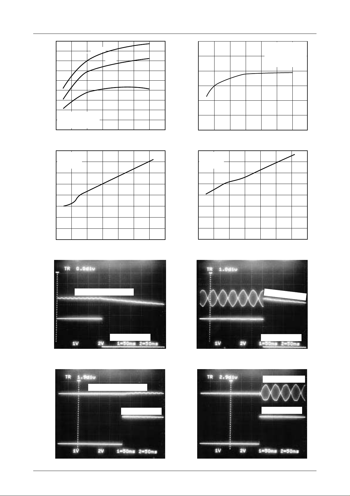
200
180
160
140
– mWVoltage, V
O
120
100
80
Output power, P
60
f=1kHz
40
THD=10%
RL=16Ω
20
—20—40
2.4
Rg=1kΩ
VIN=0
2.3
VCC=5.0V
2.2
2.1
– V
DC
2.0
PO – Ta
=6.0V
CC
V
5.0V
4.0V
(Dual Ope)
0 20 40 60 80 100
Ambient temperature, Ta – ˚C
VDC – Ta
LA4536M
16
14
12
10
8
6
Voltage gain deviation, VG – dB
4
—20—40 0 20 40 60 80 100
VG – Ta
Ambient temperature, Ta – ˚C
I
16
VIN=0
Rg=1kΩ
14
VCC=5.0V
12
CCO
– mA
10
CCO
8
VCC=5.0V
VO=–10dBm
RL=16Ω
f=1kHz
– Ta
(Dual Ope)
1.9
1.8
1.7
1.6
—40 —20 0 20 40 60 80 100
Ambient temperature, Ta – ˚C
P.SW OFF VCC=5.0V
Output AC waveform, VIN=0
P.SW DC waveform
P.SW OFF
P.SW ON VCC=5.0V
6
4
Quiescent current, I
2
0
—20 0 20 40 60 80 100
—40
Ambient temperature, Ta – ˚C
Output AC waveform
P.SW DC waveform
P.SW OFF
Output AC waveform, VIN=0
P.SW DC waveform
P.SW ON
Output AC waveform
P.SW DC waveform
P.SW ON
No.4033–7/9
Page 8
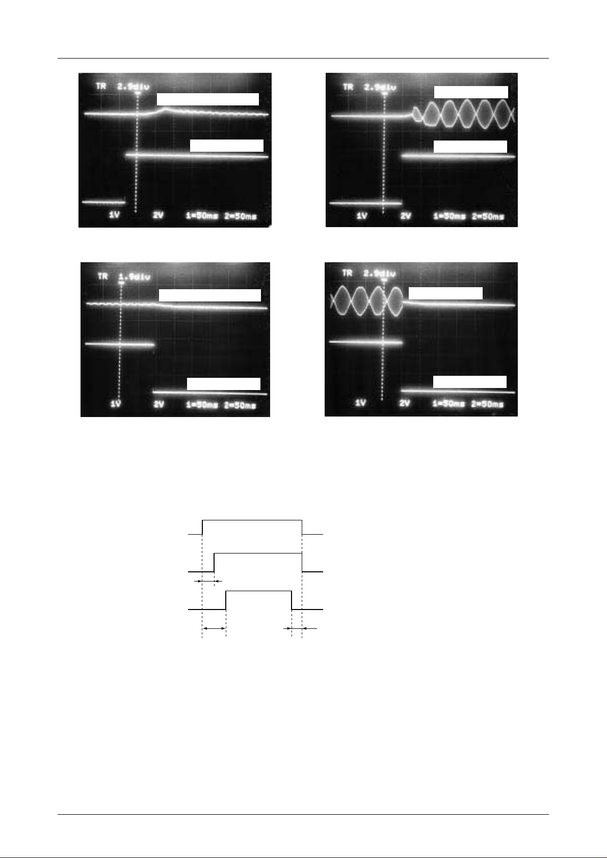
M.SW OFF
LA4536M
VCC=5.0V
M.SW ON
Output AC waveform, VIN=0
M.SW DC waveform
1V/div M.SW OFF
Output AC waveform, VIN=0
M.SW DC waveform
Output AC waveform
M.SW DC waveform
M.SW OFF
VCC=5.0V
Output AC waveform
M.SW DC waveform
1V/div M.SW ON
M.SW ON
Application Notes
Popping noise reduction
The switching sequence shown below can minimize the popping noise.
PWR.SW
V
CC
t
3
PWR, Mute SW
t
1
t
2
A11163
To minimize poping noise, the PWR mute switch should be turned on t1 (about 0.1s) after power-on and turned off t2
(about 0.1s) before power-off. Turn on and off the PWR mute switch by applying VCC with the PWR be in no state.
No.4033–8/9
Page 9
LA4536M
Specifications of any and all SANYO products described or contained herein stipulate the performance,
characteristics, and functions of the described products in the independent state, and are not guarantees
of the performance, characteristics, and functions of the described products as mounted in the customer's
products or equipment. To verify symptoms and states that cannot be evaluated in an independent device,
the customer should always evaluate and test devices mounted in the customer's products or equipment.
SANYO Electric Co., Ltd. strives to supply high-quality high-reliability products. However, any and all
semiconductor products fail with some probability. It is possible that these probabilistic failures could
give rise to accidents or events that could endanger human lives, that could give rise to smoke or fire,
or that could cause damage to other property. When designing equipment, adopt safety measures so
that these kinds of accidents or events cannot occur. Such measures include but are not limited to protective
circuits and error prevention circuits for safe design, redundant design, and structural design.
In the event that any or all SANYO products(including technical data,services) described or
contained herein are controlled under any of applicable local export control laws and regulations,
such products must not be exported without obtaining the export license from the authorities
concerned in accordance with the above law.
No part of this publication may be reproduced or transmitted in any form or by any means, electronic or
mechanical, including photocopying and recording, or any information storage or retrieval system,
or otherwise, without the prior written permission of SANYO Electric Co. , Ltd.
Any and all information described or contained herein are subject to change without notice due to
product/technology improvement, etc. When designing equipment, refer to the "Delivery Specification"
for the SANYO product that you intend to use.
Information (including circuit diagrams and circuit parameters) herein is for example only ; it is not
guaranteed for volume production. SANYO believes information herein is accurate and reliable, but
no guarantees are made or implied regarding its use or any infringements of intellectual property rights
or other rights of third parties.
This catalog provides information as of June, 2003. Specifications and information herein are subject to
change without notice.
PS No.4033–9/9
 Loading...