

Page 1
Monolithic Linear IC
Ordering number : ENN5905A
42800TN (OT)/70898RM (OT) No. 5905-1/10
SANYO Electric Co.,Ltd. Semiconductor Company
TOKYO OFFICE Tokyo Bldg., 1-10, 1 Chome, Ueno, Taito-ku, TOKYO, 110-8534 JAPAN
Two-Channel 16-W BTL General-Purpose
Audio Power Amplifier
LA4663
Overview
The LA4663 is a BTL 2-channel power amplifier IC that
was developed for ease of use in general audio
applications. In addition to providing improvements in a
wide range of electrical characteristics, the LA4663 aims
for improved listenability and an excellent costperformance ratio.
Applications
Radio/cassette players with built-in CD/MD players,
microcomponent stereo systems, active speakers,
electronic musical instruments, and other audio devices.
Features
• Wide operating supply voltage range (VCCop): 5.5 to
22 V (Certain conditions may apply.)
• High ripple rejection ratio: 60 dB (typical)
• Power: 16 W × 2 (VCC= 15 V/6Ω),
13 W × 2 (VCC= 12 V/4Ω), 6.5 W × 2 (VCC= 9 V/4Ω)
• Built-in signal muting circuit (AC muting) reduces the
number of external components and provides muting
with minimal switching noise.
• Startup circuit with a start time of 0.6 to 0.7 seconds.
The LA4663 provides distortion-free startup, since
output is only generated after the supply voltage reaches
the midpoint at power on.
(The startup time can be modified in end products by
using this circuit in conjunction with the muting circuit
described above.)
• Full complement of built-in protection circuits
(protection from shorting to ground, shorting to VCC,
load shorting, and overheating)
• High audio quality, minimal impulse noise
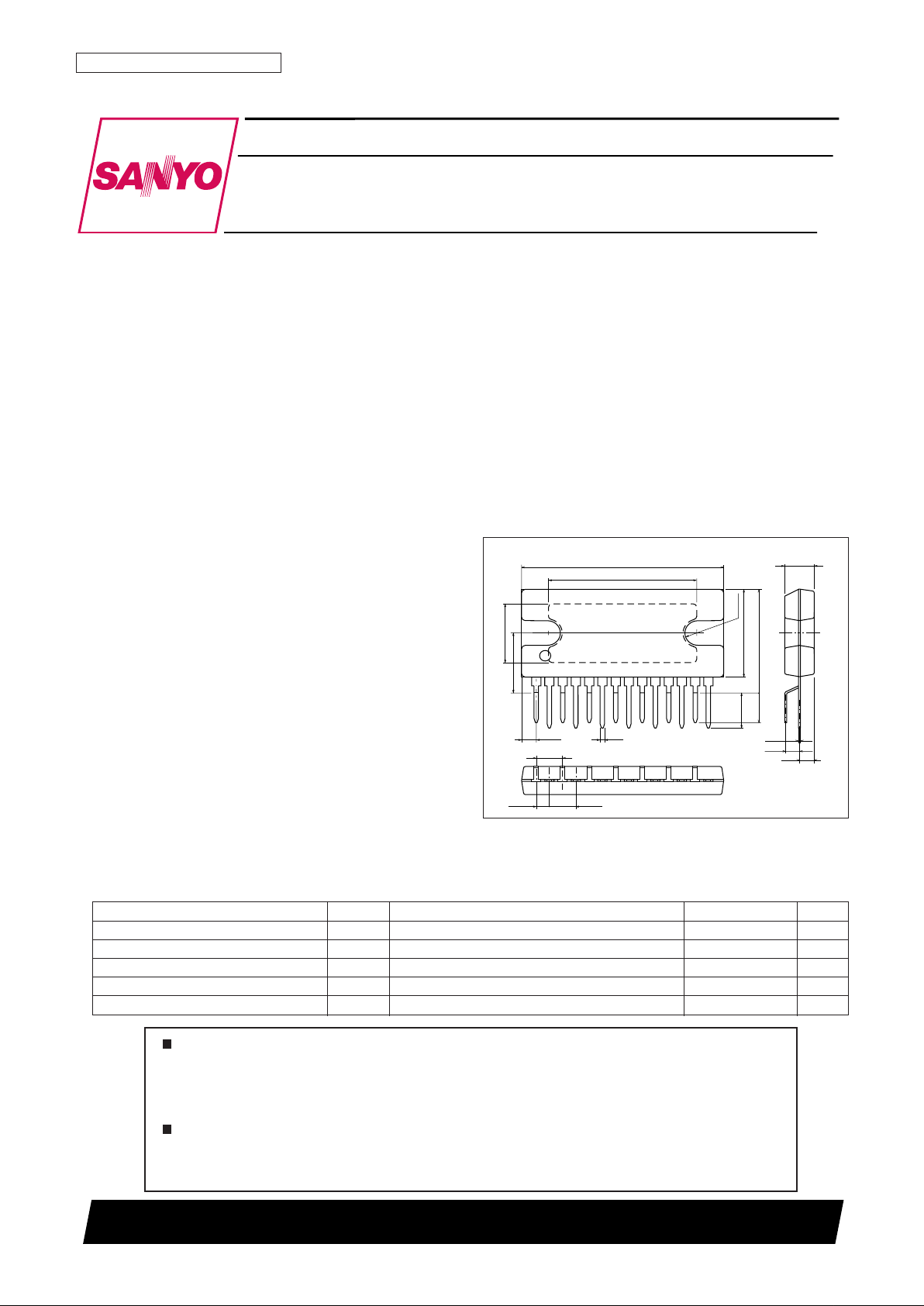
Package Dimensions
unit: mm
3113A-SIP14HZ
Specifications
Maximum Ratings at Ta = 25°C
Parameter Symbol Conditions Ratings Unit
Maximum supply voltage V
CC
max No signal 24 V
Maximum output current I
O
peak Per channel 3.5 A
Allowable power dissipation Pd max With an arbitrarily large heat sink 37.5 W
Operating temperature Topr –20 to +75 °C
Storage temperature Tstg –40 to +150 °C
27.0
20.0
R1.7
0.5
1.94
8.4
7.8
14.5max
14
1
0.4
11.8
5.2
4.6
1.6
2.2
4.0
1.78 3.56
3.56
[LA4663]
SANYO: SIP14HZ
Any and all SANYO products described or contained herein do not have specifications that can handle
applications that require extremely high levels of reliability, such as life-support systems, aircraft’s
control systems, or other applications whose failure can be reasonably expected to result in serious
physical and/or material damage. Consult with your SANYO representative nearest you before using
any SANYO products described or contained herein in such applications.
SANYO assumes no responsibility for equipment failures that result from using products at values that
exceed, even momentarily, rated values (such as maximum ratings, operating condition ranges, or other
parameters) listed in products specifications of any and all SANYO products described or contained
herein.
Page 2
Operating Conditions *1at Ta = 25°C
Note *:1. When used with VCC, RL, and output level ranges such that Pd max for the heat sink actually used is not exceeded.
2. When both channels are operating with I
O
peak values that exceed 2 A per channel.
If the I
O
peak value does not exceed 2 A per channel, a range of 5.5 to 22 V is allowed for any allowable RL(for ranges where Pd max is not
exceeded).
Operating Characteristics at Ta = 25°C, VCC= 15 V, RL= 4 Ω, f = 1 kHz, Rg = 600 Ω
No. 5905-2/10
LA4663
Parameter Symbol Conditions
Ratings
Unit
min typ max
Quiescent current I
CCO
Rg = 0, RL= open 60 100 180 mA
Standby current Ist When standby is off and with no power supply capacitor 1 10 µA
Voltage gain V
G
VO= 0 dBm 38 40 42 dB
Total harmonic distortion THD P
O
= 1 W, Filter = FLAT 0.07 0.4 %
P
O
1 VCC= 15 V, THD = 10%, RL= 4 Ω 16 20 W
Output power P
O
2 VCC= 12 V, THD = 10%, RL= 4 Ω 13 W
P
O
3 VCC= 12 V, THD = 10%, RL= 6 Ω 10 W
Output offset voltage V
N
offset Rg = 0 –300 +300 mV
Output noise voltage V
NO
Rg = 0, BPF = 20 Hz to 20 kHz 0.2 0.5 mV
Ripple rejection ratio SVRR Rg = 0, V
R
= 0 dBm, fR= 100 Hz 50 60 dB
Channel separation CH sep Rg = 10 kΩ, V
O
= 0 dBm 50 60 dB
Input resistance Ri 14 20 26 kΩ
Standby pin applied voltage V
ST
Amplifier on (the pin 5 voltage) 2.5 10 V
Muting pin applied voltage V
M
Muting on (the pin 6 voltage) 1.5 3 V
Muting attenuation ATT
M
Muting on (VO= 1 V rms), BPF = 20 Hz to 20 kHz 70 80 dB
Parameter Symbol Conditions Ratings Unit
Recommended supply voltage V
CC
12, 15 V
Recommended load resistance range R
L
op 4 to 8 Ω
When R
L
= 8 Ω 5.5 to 21 V
Allowable operating supply voltage range *
2
VCCop
When R
L
= 6 Ω 5.5 to 20 V
When R
L
= 5 Ω 5.5 to 17 V
When R
L
= 4 Ω 5.5 to 15 V
0
10
15
13.9
20.8
10.4
3.1
5
30
20
25
40
35
80 160120100 140604020-20 0
2
3
2
3
5
7
10
100
2 3 5 7
1000
2 3 5 7
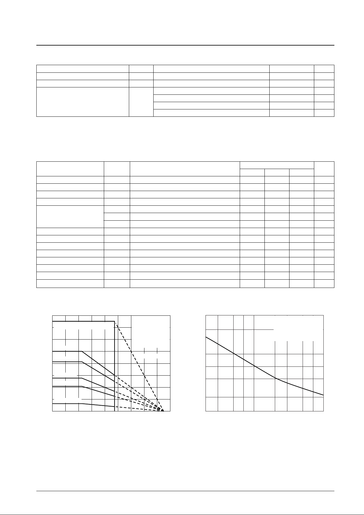
Pd max-Ta
θf=3°C/W
θjc=2°C/W
θf=4°C/W
θf=7°C/W
θf=10°C/W
No radiator fin
θf
-
S
f
Allowable power dissipation, Pd max — W
Ambient temperature, Ta — °C
With an arbitrarily large heat sink
With an Al heat sink
with mounting bolts
tightened down with
a torque of 39 N·cm
and silicone grease
applied.
Al heat sink, t = 1.5 mm
With mounting bolts
tightened down with a
torque of 39 N·cm and
silicone grease applied.
Heat sink area, Sf— cm
2
Heat sink thermal resistance, θ
f
— °C/W
Page 3

Usage Notes
1. Maximum ratings
If the device is operated in the vicinity of the maximum ratings, it is possible for small changes in the operating
conditions to result in the maximum ratings being exceeded. Since this can result in destruction of the device,
applications should be designed with adequate margins in the supply voltage and other parameters so that the maximum
ratings are never exceeded during device operation.
2. Protection circuits
While the LA4663 includes a full complement of built-in protection circuits, care is required in the usage. In particular,
be careful not to short any pairs of device pins together.
[Notes on the shorting (power, ground, and load shorting) protection circuit]
• This protection circuit operates whenever a power short (a short between the output and VCC), a ground short (a short
between the output and ground), or a load short (shorting between the + and – outputs) is detected. Although there are
cases where the protection circuit may not operate if the supply voltage is under 9 V, the thermal protection circuit will
protect the device in this range.
• The protection circuit continues to operate during the interval that the abnormal short continues, and automatically
recovers when the error state is resolved. However, under certain usage conditions, there are situations where the
protection circuit may lock and remain locked even after the problem has been resolved. In these cases, the circuit can
be reset by switching to standby mode or turning off the power temporarily.
• If the output is shorted to VCCwith the IC in the standby state and furthermore, a VCCof 20 V or higher applied, an
offset will be created between the + and – outputs. If a load is connected in this state, a current will flow in that load,
and the IC may be destroyed. Applications should assure that this does not occur.
• In the following situations, the operation of the protection circuit may result in a sound switching phenomenon at high
output levels. This may be a problem, depending on the details of the end product circuit itself, and must be verified in
an actual system.
• At low load resistances RL(high loads) and at high VCCvoltages, and with both channels operating at IOpeak levels of
over 2 A per channel. (This phenomenon is more likely to occur the higher the chip temperature.)
For systems operating under the most sever conditions (high temperatures and high outputs), specific operating
conditions such that the above phenomenon does no occur are listed in the “Allowable operating supply voltage range
(VCCop)” item in the Operating Conditions section of the specifications. (Refer to the VCCop ranges for different R
L
values.)
[Thermal protection circuit]
• A thermal protection circuit is provided to prevent damage to or destruction of the IC itself when the IC generates
abnormally high temperatures. This means that gradual attenuation is applied to the output signals by the thermal
protection circuit if the IC junction temperature (Tj) rises above about 160°C due to insufficient heat sinking or other
problems.
3. Notes on printed circuit boards
• When designing the printed circuit board pattern, keep the input lines separated from both the VCC lines and the
output lines. This is to prevent increased distortion and oscillation.
• When high output levels are used, make power-ground lines as wide as possible and as short as possible to prevent the
PWR GND pins potential from increasing with respect to pre-ground. (From the standpoint of IC stability, ideally, the
ground pin potential should be the lowest potential in the system. This is to prevent trouble caused by several types of
induced parasitic devices due to increases in the GND pin potential due to the structure of the IC.)
No. 5905-3/10
LA4663
Page 4

4. Notes on heat sink mounting
• Use a tightening torque of between 39 and 59 N·cm.
• Make the spacing of the heat sink mounting screw holes the same as the spacing of the IC mounting screw holes. Also,
make the mounting screw hole spacing as short as possible within the range that still allows mounting, referring to the
external dimensions L and R.
• For mounting screws, use screws that correspond to either the truss screws or binding screws stipulated by the JIS
(Japan Industrial Standards). Use washers to protect the IC case.
• Do not allow any foreign matter, such as machining chips, to get between the IC (package internal) heat sink and the
external heat sink. Also, if grease is applied to the junction, apply the grease as evenly as possible.
5. Other notes
• The LA4663 is a BTL power amplifier IC. When connecting this IC to test equipment, do not allow the test equipment
grounds for the input and output systems to be shared grounds.
No. 5905-4/10
LA4663
+ +
R
L
A10629
Page 5
No. 5905-5/10
LA4663
+
–
–+
6
5
14
2
+
–
12
13
R1
22 kΩ
C4
10 µF
10 V
+
–
C3
47 µF
25 V
+
–
C5
2200 µF
25 V
C1
4.7 µF
10 V
+5 V
Ri =
20 kΩ
SIGNAL
MUTE
IN1
3
1
PRE
GND
PWR
GND1
–OUT1
+OUT1
C6
0.1 µF
C7
0.1 µF
R2
2.2 Ω
R3
2.2 Ω
RL = 4 to 8 Ω
–+
9
4
+
–
11
10
C2
4.7 µF
10 V
Ri =
20 kΩ
IN2
PWR
GND2
–OUT2
+OUT2
C8
0.1 µF
C9
0.1 µF
R4
2.2 Ω
R5
2.2 Ω
**
**
**
**
RL = 4 to 8 Ω
CH 1
CH 2
Ripple Filter/
Starting Time
7 8
+5 V
STAND BY VCC1 VCC2
V
CC
A10630
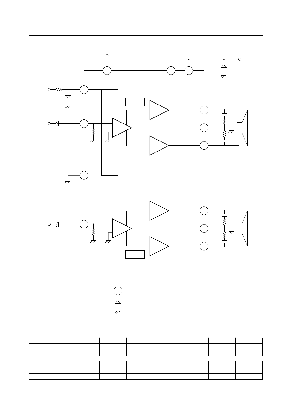
Pin No. 1 2 3 4 5 6 7
Pin RF IN1 PRE-GND IN2 STAND-BY MUTE V
CC
1
Pin voltage (V) 14.32 3 m 0 3 m 5 21m 15
Pin No. 8 9 10 11 12 13 14
Pin V
CC
2 +OUT2 PWR-GND2 –OUT2 –OUT1 PWR-GND1 +OUT1
Pin voltage (V) 15 6.84 0 6.84 6.84 0 6.84
Equivalent Circuit Block Diagram
Pin Voltages at VCC= 15 V, with 5 V applied to the STBY pin (pin 5), using a digital volt meter.
Input amplifier
Input amplifier
Output amplifier
V
CC
/ground shorting protection
circuit
Load shorting protection circuit
Thermal protection circuit
— Protection circuits —
Output amplifier
Polyester film capacitors
* *
Page 6
External Components
C1 and C2
• These are input coupling capacitors, and we recommend that values under 4.7 µF be used. The LA4663 uses a zero
bias type input circuit, and the input pin potential is about zero volts. Determine the polarity orientation of these
capacitors based on the DC current from the circuit connected to the LA4663 front end.
If the potential difference between across the + and – leads on the input capacitors is large, the charge time for the
input capacitors can be reduced by using as small a value as possible without causing degradation of the low band
frequency characteristics. This will shorten the time required to reach stable operation when power is first applied.
C3 *
1
• This capacitor functions both as a ripple filter and as the amplifier starting time capacitor. We recommend a value of
47 µF. When the recommended value is used, the BTL SVRR between outputs will be about 63 dB, and that between
the outputs and ground will be about 47 dB. (These are values are for reference purposes.) Similarly, the starting time
(the time between the point power is first applied and the point an output is generated) will be around 0.6 to 0.7
seconds.
C4 and R1 *
2
• These form an CR circuit used for muting function smoothing. C4 is required even if the muting function is not used.
C5
• Power supply capacitor
C6 to C9 and R2 to R5
• These components for oscillation prevention CR circuits. We recommend the use of polyester film capacitors (Mylar
capacitors) with excellent temperature characteristics for C6 through C9. (R2 to R5 should all be 2.2-Ω 1/4-W
resistors.)
Notes: 1. Starting time
• The LA4663 includes a built-in starting time circuit. The starting time can be varied somewhat by modifying
the value of the external capacitor connected to pin 1. With the recommended value of 47 µF, the starting time
will be between 0.6 and 0.7 second (although this will vary with the supply voltage, VCC) and this time can be
lengthened to about 0.9 second by inserting a 10 µF capacitor in parallel.
• We do not recommend using a value smaller than the recommended value for the pin 1 capacitor, since that
could result in reducing the SVRR with respect to ground.
2. Signal muting function
• When the recommended CR circuit (10 µF and 22 kΩ) is connected to pin 6, the signal muting function can be
turned on, and a muting function with minimal impulse noise applied by applying a voltage of 5V.
• The CR circuit determines the attack and recovery times for smoothing function. Note that this 10-µF capacitor
is required even when the signal muting function is not used, since it is also used for smoothing after the
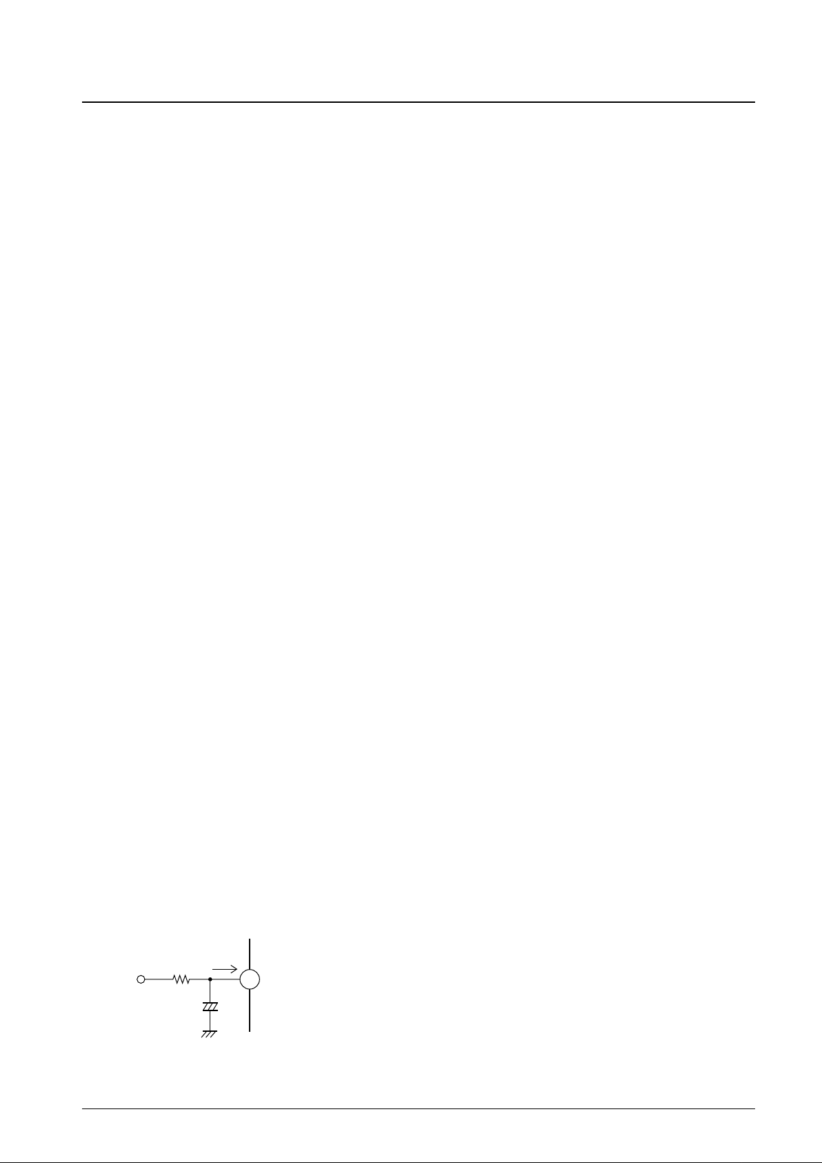
starting time has elapsed.The influx current to pin 6 when this external resistor has a value of
22 kΩ will be about 170 µA when the applied voltage is +5
V. Although it is possible to modify the value of this resistor
if a different applied voltage or if the capacity of the
microcontroller required it, it is possible for the level of the
impulse noise associated with the muting function to increase
if the pin 6 influx current becomes excessive. Be sure to take
this influx current into account if the value of this resistor is
modified.
No. 5905-6/10
LA4663
+
–
6
+5 V
22 kΩ
10 µF
I
About 1.56 V
A10631
Page 7
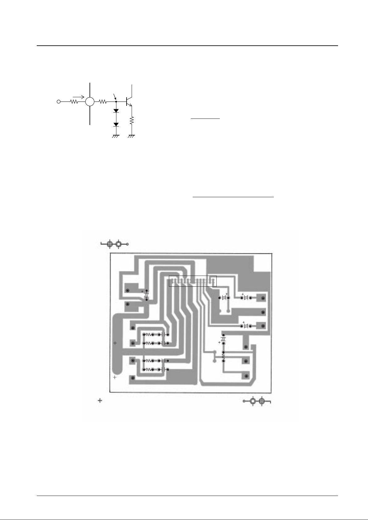
Other Notes
• Standby function
Pin 5 in this IC is the standby pin, and applying a voltage of 2.0 V or
higher will activate this function. The pin 5 influx current for an
applied voltage of 5 V will be about 240 µA.
ISTB =
5 V – 1.4 V
= 240 µA
15 k
Insert an external current limiting resistor (RSTB) if it is necessary to
limit this influx current when using a microcontroller.
If this input voltage is applied by a circuit or device other than a
microcontroller, calculate the value for RSTB from the following
formula such that the pin 5 influx current due to the applied VSTB is
under 500 µA.
RSTB =
Applied voltage (VSTB) – 1.4 V
– 15 kΩ
500 µA
No. 5905-7/10
LA4663
5
V
STB
(R
STB)
I
STB
About 1.4 V
15 kΩ
A10632
C1
GND
STBY
MUTE
C4
R1
IN1
PRE-GND
IN2
C2
C3
14
1
C5
C7R3
C6R2
C9R5
C8R4
—OUT1
OUT1
—OUT2
OUT2
GND
V
CC
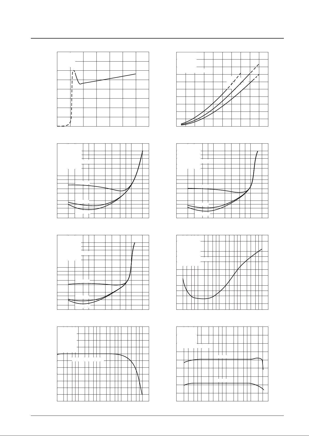
Sample Printed Circuit Board Pattern (Copper surface)
Page 8
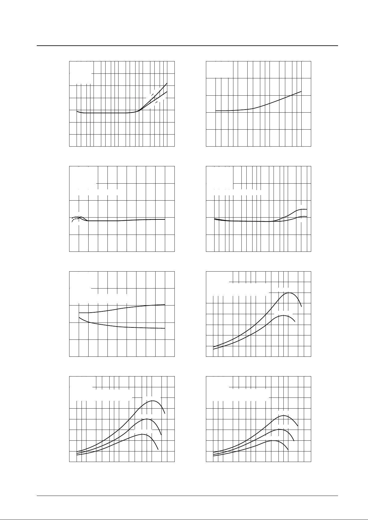
No. 5905-8/10
LA4663
0
0
20
4 8 12 16 20 24 28
40
60
80
100
120
160
140
0
4
2
3
5
7
0.1
2
3
5
7
1.0
2
2
3
5
7
10
4
0.1 1.0
2 3 5 7
10
2 3 5 7 2 3
6 8 10 12 14 16 18 20 22 24
8
12
16
20
24
36
32
28
40
2
3
5
7
0.1
2
3
5
7
1.0
2
2
3
5
7
10
0.1 1.0
2 3 5 7
10
2 3 5 7 2 3
2
3
5
7
0.1
2
3
5
7
1.0
2
2
3
5
7
10
0.1 1.0
2 3 5 7
10
2 3 5 7 2 3
2
3
5
7
0.1
2
3
2
3
5
7
1.0
10 100
2 3 5 71k2 3 5 7
10k
2 3 5 7
100k
2 3 5 7 2
-7
-6
-5
-4
-3
-2
-1
3
4
0
1
2
10 100
2 3 5 71k2 3 5 7
10k
2 3 5 7
100k
2 3 5 7 2
12
14
16
18
20
22
10
28
24
26
10 100
2 3 5 71k2 3 5 7
10k
2 3 5 7 2 3 5
I
CCO
-
V
CC
THD-P
O (RL=4Ω)
THD-P
O (RL=6Ω)
PO-
V
CC
THD
-
f
f
Response
P
O
-
f
RL=Open
Rg=0
V
STB
=5V
f=1kHz
THD=10%
Rg=600Ω
R
L
=4Ω
R
L
=6Ω
R
L
=8Ω
VCC=15V
RL=4Ω
Rg=600Ω
Filter=FLAT
VCC=15V
RL=6Ω
Rg=600Ω
Filter=FLAT
VCC=15V
RL=4Ω
Rg=600Ω
PO=1W
Filter=FLAT
f=10kHz
f=1kHz
f=100Hz
f=10kHz
f=1kHz
f=100Hz
f=10kHz
f=1kHz
f=100Hz
VCC=15V
RL=8Ω
Rg=600Ω
Filter=FLAT
VCC=15V
RL=4Ω
Rg=600Ω
VO=0dBm
VCC=15V
RL=4Ω
Rg=600Ω
THD=10%
THD=1%
THD-P
O (RL=8Ω)
Quiescent current, I
CCO
— mA
Output power, P
O
— W
Total harmonic distortion, THD — %
Total harmonic distortion, THD — %
Supply voltage, VCC— V
Supply voltage, V
CC
— V
Output power, P
O
— W Output power, PO— W
Both channels operating
Both channels operating
Both channels operating
Total harmonic distortion, THD — %
Response — dB
Total harmonic distortion, THD — %
Output power, P
O
— W
Output power, PO— W
Input frequency, f — Hz
Input frequency, f — Hz
Input frequency, f — Hz
Both channels operating
Both channels operating
Both channels operating
Both channels operating
Page 9
No. 5905-9/10
LA4663
-90
-20
-80
-70
-60
-30
-50
-40
10 100
2 3 5 71k2 3 5 7
10k
2 23 5 7
100k
72 3 5
-100
0
-20
-80
-60
-40
10 100
2 3 5 71k2 3 5 7
10k
2 3 5 7 72 3 5
0
0.1
0.2
0.3
0.4
0.5
100
2 3 5 7
1k
2 3 5 7
100k10k
2 3 5 7 2
-100
-80
-60
-40
-20
0
64 8 10 12 14 16 18 20 2422 26
-100
-80
-60
-40
-20
0
0.20 0.4 0.6 0.8 1.0 1.2 1.4 1.6 2.01.8 2.2
0
32
24
28
4
8
12
20
16
0.1
5 7
1.0
2 33 5 7
10
2 3 5 7 2 3 5
0
32
24
28
4
8
12
20
16
0.1
5 7
1.0
2 33 5 7
10
2 3 5 7 2 3 5
0
32
24
28
4
8
12
20
16
0.1
5 7
1.0
2 33 5 7
10
2 3 5 7 2 3 5
CHsep.-f
SVRR
-
V
CC
VNO-
R
g
SVRR
-
f
R
VCC=15V
RL=4Ω
Rg=10kΩ
VO=0dBm
RL=4Ω
Rg=0
fR=100Hz
V
CCR
=0dBm
VCC=15V
RL=4Ω
Rg=0
fR=100Hz
VCC=15V
RL=4Ω
Rg=0
V
CCR
=0dBm
VCC=15V
RL=4Ω
DIN AUDIO
CH1
CH2
CH1
CH2
VCC=15V
VCC=12V
CH1 CH2
CH2 CH1
SVRR-V
CCR
Pd-
P
O (RL=4Ω)
f=1kHz
RL=4Ω
VCC=18V
VCC=15V
VCC=12V
Pd-
P
O (RL=6Ω)
f=1kHz
RL=6Ω
VCC=18V
VCC=15V
VCC=12V
Pd-
P
O (RL=8Ω)
f=1kHz
RL=8Ω
Channel separation, CHsep. — dB
Output noise voltage, V
NO
— mV rms
Ripple rejection ratio, SVRR — dB
Ripple rejection ratio, SVRR — dB
Input frequency, f — Hz Input resistance, Rg — Ω
Supply voltage, V
CC
— V
Ripple frequency, fR— Hz
With a 1-µF power supply capacitor
With a 1-µF power supply capacitor
Ripple rejection ratio, SVRR — dB
Power dissipation, Pd — W
Power dissipation, Pd — W
Power dissipation, Pd — W
Output power, PO— W
Power supply ripple voltage, V
CCR
— V rms
Output power, P
O
— W
Output power, P
O
— W
With a 1-µF power supply capacitor
Calculated as SVRR = 20·log V
O/VCCR
Both channels operating
Calculated as Pd = V
CC
× ICC– 2·P
O
Both channels operating
Calculated as Pd = V
CC
× ICC– 2·P
O
Both channels operating
Calculated as Pd = V
CC
× ICC– 2·P
O
Page 10
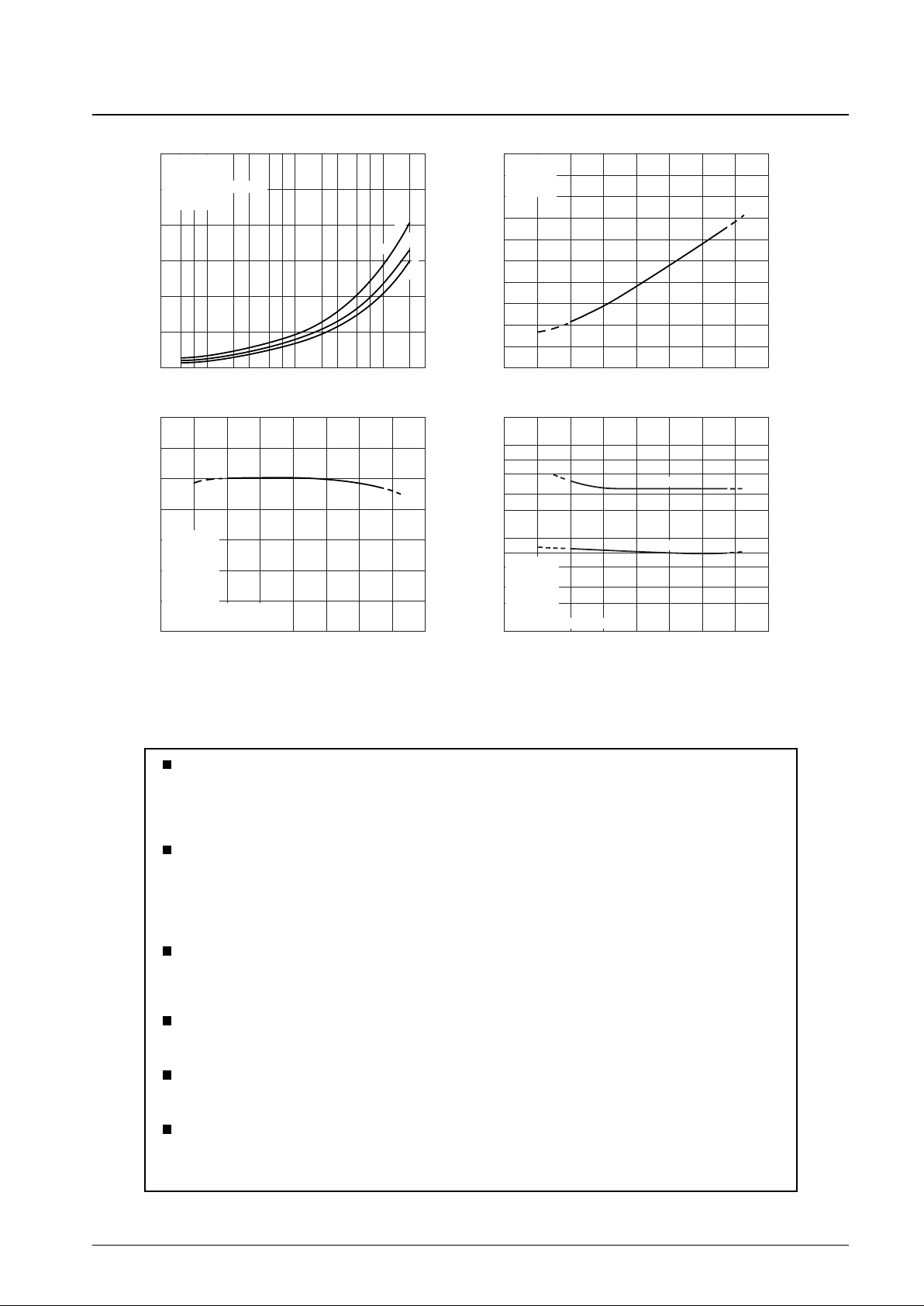
PS No. 5905-10/10
LA4663
This catalog provides information as of April, 2000. Specifications and information herein are subject to
change without notice.
Specifications of any and all SANYO products described or contained herein stipulate the performance,
characteristics, and functions of the described products in the independent state, and are not guarantees
of the performance, characteristics, and functions of the described products as mounted in the customer’s
products or equipment. To verify symptoms and states that cannot be evaluated in an independent device,
the customer should always evaluate and test devices mounted in the customer’s products or equipment.
SANYO Electric Co., Ltd. strives to supply high-quality high-reliability products. However, any and all
semiconductor products fail with some probability. It is possible that these probabilistic failures could
give rise to accidents or events that could endanger human lives, that could give rise to smoke or fire,
or that could cause damage to other property. When designing equipment, adopt safety measures so
that these kinds of accidents or events cannot occur. Such measures include but are not limited to protective
circuits and error prevention circuits for safe design, redundant design, and structural design.
In the event that any or all SANYO products (including technical data, services) described or contained
herein are controlled under any of applicable local export control laws and regulations, such products must
not be exported without obtaining the export license from the authorities concerned in accordance with the
above law.
No part of this publication may be reproduced or transmitted in any form or by any means, electronic or
mechanical, including photocopying and recording, or any information storage or retrieval system,
or otherwise, without the prior written permission of SANYO Electric Co., Ltd.
Any and all information described or contained herein are subject to change without notice due to
product/technology improvement, etc. When designing equipment, refer to the “Delivery Specification”
for the SANYO product that you intend to use.
Information (including circuit diagrams and circuit parameters) herein is for example only; it is not
guaranteed for volume production. SANYO believes information herein is accurate and reliable, but
no guarantees are made or implied regarding its use or any infringements of intellectual property rights
or other rights of third parties.
0
6
5
1
2
4
3
0.1
5 7
1.0
2 33 5 7
10
0.01
0.1
2 3 5 7 2
2
3
5
7
1.0
2
2
3
5
7
3
20
220
60
40
100
180
140
200
80
160
120
0-40 -20 20 40-60 60 80 100
0
8
4
16
24
12
28
20
0-40 -20 20 40-60 60 80 100
0-40 -20 20 40-60 60 80 100
ICC-
P
O
VCC=15V
Rg=600Ω
f=1kHz
R
L
=4Ω
R
L
=6Ω
R
L
=8Ω
I
CCO
-
Ta
RL=Open
Rg=0
VCC=15V
PO-
Ta
VCC=15V
RL=4Ω
THD=10%
Rg=600Ω
f=1kHz
VCC=15V
RL=4Ω
Rg=600Ω
f=1kHz
PO=1W
THD
-
Ta
f=10kHz
f=1kHz
Current drain, I
CC
— A
Output power, P
O
— W
Total harmonic distortion, THD — %
Quiescent current, I
CCO
— mA
Output power, PO— W
Ambient temperature, Ta — °C Ambient temperature, Ta — °C
Ambient temperature, Ta — °C
Both channels operating
Both channels operating
With a 3°C/W heat sink
Both channels operating
 Loading...