

Page 1
Ordering number: EN5245A
Monolithic Linear IC
LA4708
20 W 2-channel BTL AF Power Amplifier
for Car Stereos
Overview
The LA4708 is a BTL two-channel power IC for car audio
developed in pursuit of excellent sound quality. Low-region
frequency characteristics have been improved through the use
of a new NF capacitorless circuit, and crosstalk which causes
‘‘muddy’’ sound has been reduced by improving both circuit
and pattern layout. As a result, the LA4708 provides powerful
bass and clear treble. In addition, the LA4708 features on-chip
protectors and standby switch. The LA4708 is also
pin-compatible with the LA4705NA (car stereo-use 17 W
two-channel power IC), and can be substituted for the
LA4705NA for higher power. (When the board is shared, pins
1 and 9 must be left open.)
Features
.
High power: supports total output of 30 W + 30 W
(V
= 13.2 V, THD = 30%, RL=4Ω)
CC
.
Supports RL=2Ω(PO= 30 W when VCC= 13.2 V,
THD = 10%)
.
Designed for excellent sound quality
(f
< 10 Hz, fH= 130 kHz)
L
.
NF capacitorless
.
Any on time settable by external capacitor
.
Less pop noise
.
Standby switch circuit on chip (microprocessor supported)
.
Various protectors on chip
(output-to-ground short/output-to-V
load short/overvoltage/thermal shutdown circuit)
CC
short/
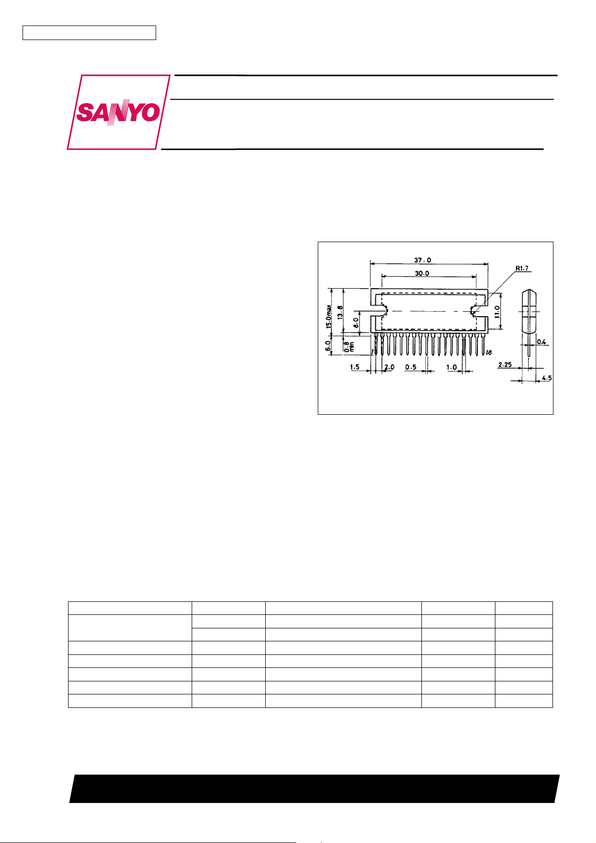
Package Dimensions
unit: mm
3109-SIP18H
[LA4708]
SANYO : SIP18H
Specifications
Maximum Ratings at Ta = 25°C
Parameter Symbol Conditions Ratings Unit
Maximum supply voltage V
Surge supply voltage V
Maximum output current I
Allowable power dissipation Pd max Arbitrarily large heat sink 37.5 W
Operating temperature Topr –35 to +85 °C
Storage temperature Tstg –40 to +150 °C
* Set VCC,RLin a range that does not exceed Pd max = 37.5 W
max 1 No signal,t=60s 24 V
CC
V
max 2 16 V
CC
surge t % 0.2 s, single giant pulse 50 V
CC
peak Per channel 4.5 A
O
SANYO Electric Co.,Ltd. Semiconductor Bussiness Headquarters
TOKYO OFFICE Tokyo Bldg., 1-10, 1 Chome, Ueno, Taito-ku, TOKYO, 110 JAPAN
93096HA(II)/13096HA(II) No.5245-1/9
Page 2
LA4708
Operating Conditions at Ta = 25°C
Parameter Symbol Conditions Ratings Unit
Recommended supply voltage V
Operating voltage range V
Recommended load resistance R
Recommended load resistance range
CC
op Range where Pd max is not exceeded 9 to 16 V
CC
L
RLop 2to4 Ω
Operating Characteristics at Ta = 25°C, VCC= 13.2 V, RL=4Ω,f=1kHz, Rg = 600 Ω
Parameter Symbol Conditions min typ max Unit
Quiescent current I
Standby current Ist 10 60 µA
Voltage gain VG 38 40 42 dB
Total harmonic distortion THD P
Output power
Output offset voltage V
Output noise voltage V
Ripple rejection ratio SVRR Rg = 0, f
Channel separation CHsep Rg = 10 kΩ,V
Input resistance r
Standby pin applied voltage Vst Amp on, applied through 10 kΩ 2.5 V
CCO
= 2 W 0.07 0.4 %
1 THD = 10% 16 20 W
P
O
P
2 THD = 10%, VCC= 14.4 V 24 W
O
P
3 THD = 10%, RL=2Ω 30 W
O
offset Rg = 0 –300 +300 mV
N
NO
i
O
Rg = 0, B.P.F. = 20 Hz to 20 kHz 0.1 0.5 mVrms
= 100 Hz, VR= 0 dBm 40 50 dB
R
= 0 dBm 50 60 dB
O
13.2 V
4 Ω
70 150 250 mA
21 30 39 kΩ
CC
V
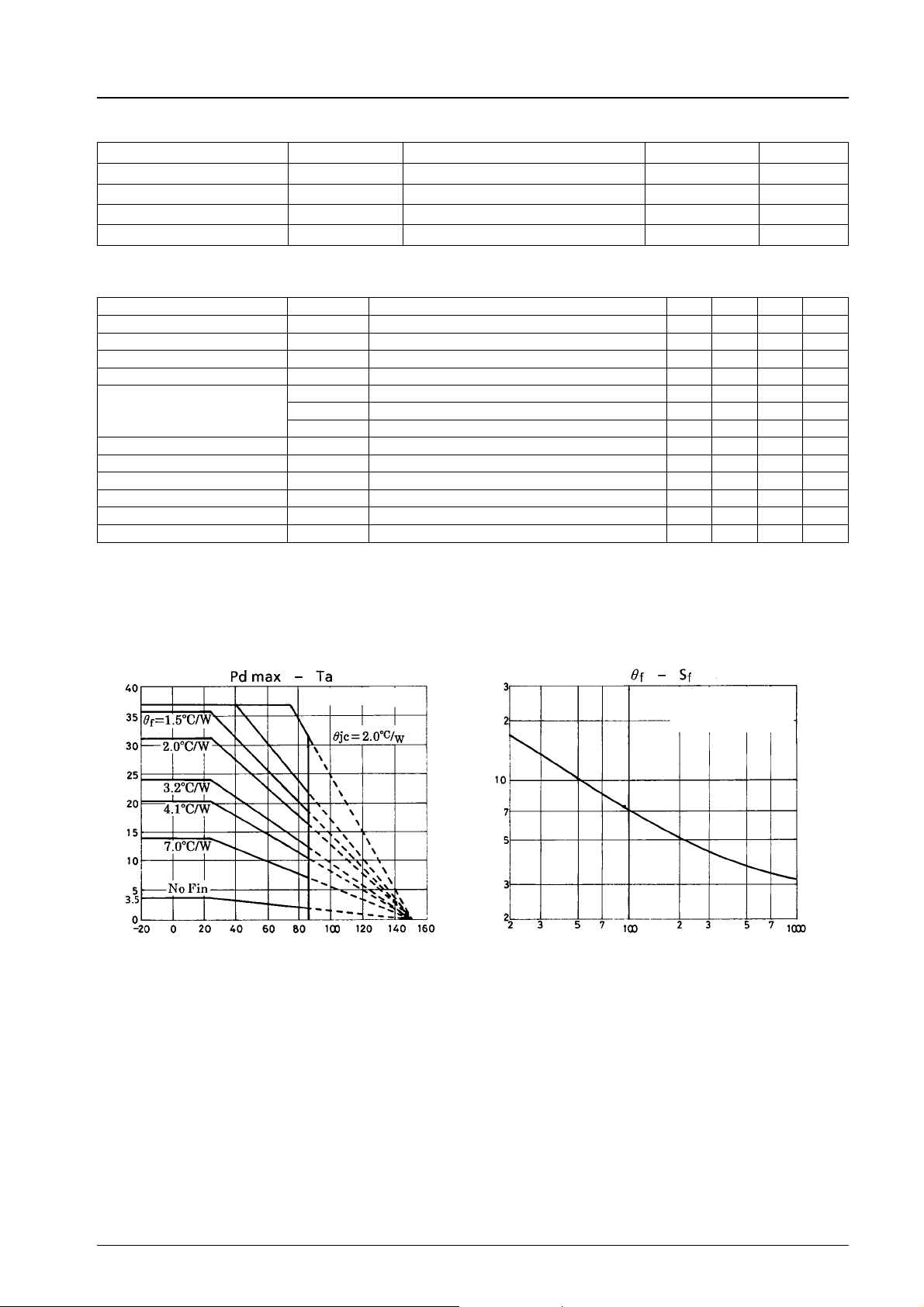
Allowable power dissipation, Pd max — W
Arbitrarily large heat sink
Ambient temperature, Ta — °C
— °C/W
f
Heat sink thermal resistance, θ
Al heat sink, t = 1.5 mm
Tightening torque 39 Nccm
With silicone grease applied
Heat sink area, Sf—cm
2
No.5245 -2/9
Page 3
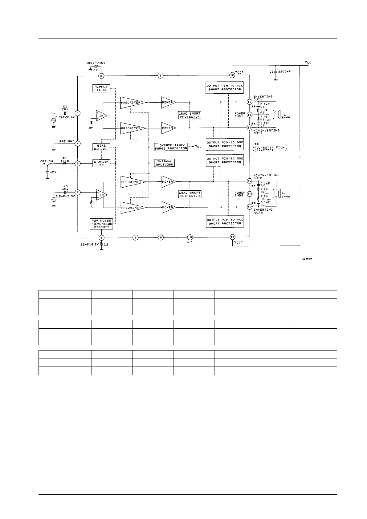
Equivalent Circuit Block Diagram
LA4708
--
--
Pins 1,9 : Don’t use
Pin 10 : No connection
Each Pin Voltage
VCC= 13.2 V, 5 V applied through STBY = 10 kΩ,RL=4Ω,Rg=0
PinNo.123456
Name IN1 DC Pre-GND STBY ON TIME
Pin voltage (V) 0.29 1.58 6.55 0 3.2 2.28
Pin No. 7 8 9 10 11 12
Name IN2 POP – N.C V
Pin voltage (V) 1.58 2.08 0.29 0 13.2 6.5
Pin No. 13 14 15 16 17 18
Name PWR–GND 2 +OUT 2 +OUT 1 PWR–GND 1 –OUT 1 V
Pin voltage (V) 0 6.5 6.5 0 6.5 13.2
2 –OUT 2
CC
CC
1
No.5245 -3/9
Page 4
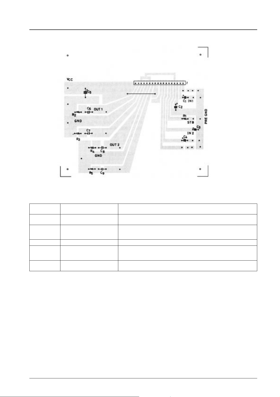
Sample Print Pattern
LA4708
Copper foil area 90 × 105 mm
2
Description of External Components
C1, C4 Input capacitors 2.2µF is recommended. fLcan be varied by C1, C4 capacitances to adjust the
C2 Decoupling capacitor
(ripple filter)
C3 Amplifier on time setting
capacitor
C5 Power supply capacitor
C6, C7, C8, C9 Oscillation blocking capacitors Use polyester film capacitors (Mylar capacitors) with good temperature
R1 Standby switch current limiting
resistor
bass range.
Approximately 0.8 second for 33 µF. Since the on time is proportional to this
capacitance, it can be set as desired by varying this capacitance.
(Refer to the characteristics curve.)
characteristics. (R2, R3, R4, and R5 used jointly.) Since stability may be
affected slightly by the pattern layout, etc., 0.1 µF or more is recommended.
10 kΩ is recommended (when the applied voltage for the standby switch is
2.5 V to 13.2 V). This resistor cannot be removed.
No.5245 -4/9
Page 5
LA4708
Features of IC Inside and Usage Notes
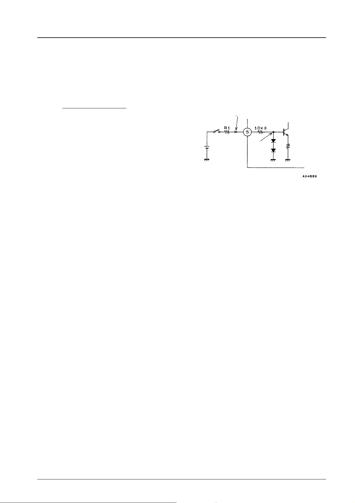
Standby function
.
Pin 5 is the standby switch pin. The amplifier is turned on by applying approximately 2.5 V or more to this pin through an
external resistor (R1).
.
If voltage in excess of 13.2 V is to be applied to the standby switch, calculate the value of R1 using the following formula so
that the current flowing into pin 5 is 500 µA or less:
R1 =
Mute function
.
Pin 6 is the connector for the capacitor that determines the on time in order to prevent pop noise. By grounding this pin, the
amplifier can implement mute operation. In this case, the recovery time depends on C3.
How to reduce pop noise
.
Although the LA4708 reduces pop noise, an electrolytic capacitor of between 0.47 and 2.2 µF can be connected between pin 8
and the pre-GND to further reduce pop noise that occurs when power supply is turned on/off (standby switch on/off). The larger
the capacitance, the lower the frequency of pop noise, and it is barely audible, but sound residue of the sound signal is liable to
linger when power is turned off. Pin 8 is the bias pin for the output amplifier and normally is left open.
Protectors
.
In an output-to-ground and output-to-VCCshort protector system configuration, if a DC resistor is connected between amplifier
output pin and GND, the protector may operate, causing the amplifier not to start operating. Therefore, as a general rule, no DC
resistor should be connected between amplifier output pin and GND.
.
In order to prevent damage or degradation which may be caused by abnormally heated IC, the LA4708 has a thermal shutdown
protector. Accordingly, if the IC junction temperature (Tj) climbs to around 170 to 180°C due to inadequate heat dissipation, the
thermal shutdown protector will operate to control the output gradually into attenuation.
.
Also be fully careful of handling other protectors built in the LA4708.
Applied voltage − 1.4 V
500 µA
–10kΩ
500 µA or less
Standby
applied voltage
About 1.4 V
)
(2V
BE
Pin 5 Equivalent
circuit internal IC
Miscellaneous
.
Since pins 1 and 9, which are unused, are connected internally, they must be left open.
.
Pin 10 is an NC pin (no internal connection).
No.5245 -5/9
Page 6
LA4708
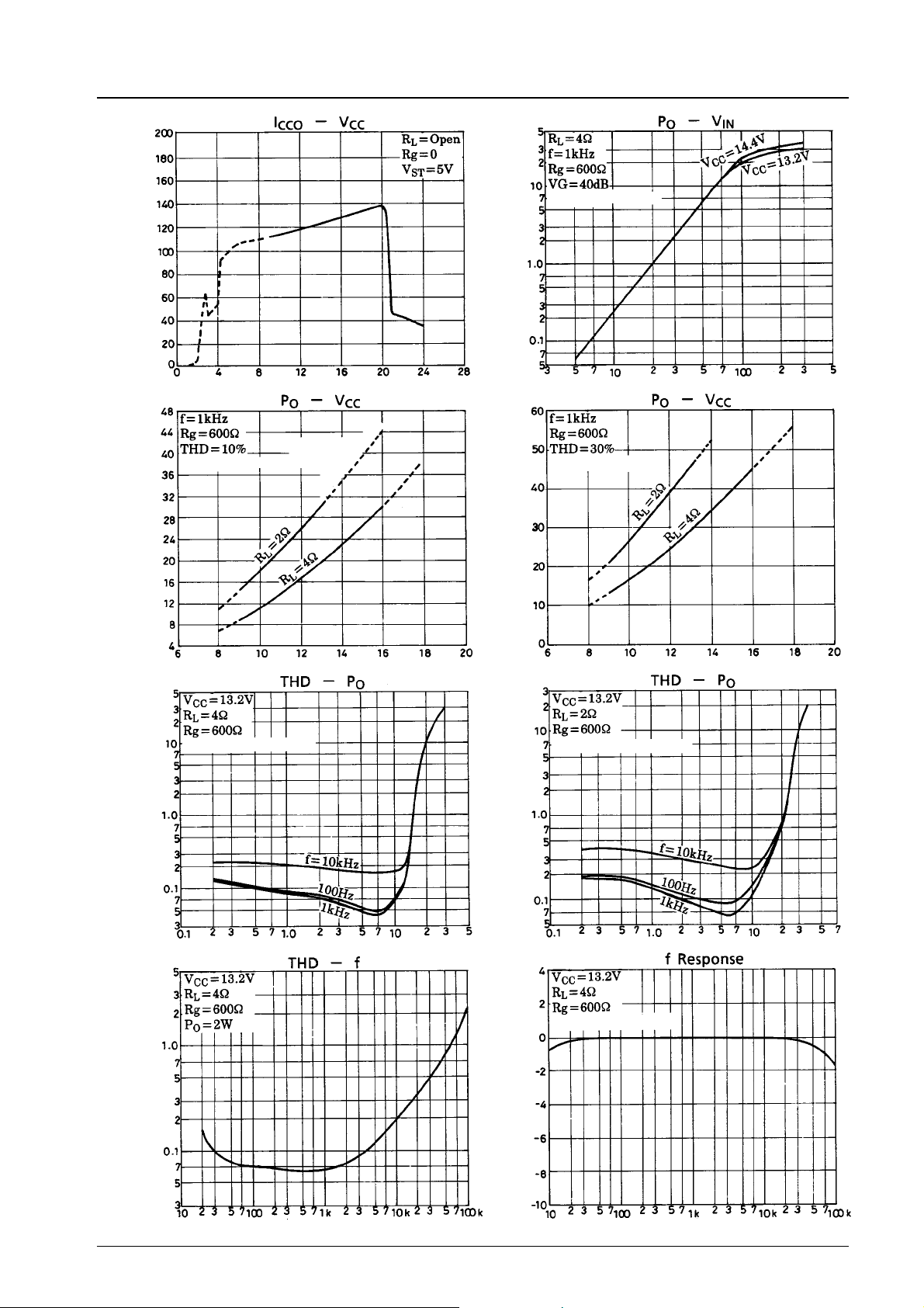
Dual channel drive
CCO—mA
Quiescent current, I
—W
O
Output power, P
Dual channel drive
—W
O
Output power, P
Dual channel drive
Supply voltage, VCC—V
Exceeding
Pd max
Supply voltage, VCC—V
Input level, VIN— mVrms
Dual channel drive
—W
O
Output power, P
Supply voltage, VCC—V
Dual channel drive
Total harmonic distortion, THD — %
Output power, P
O
—W
Total harmonic distortion, THD — %
VO=0dBmatf=1kHz
Output power, P
O
—W
Response — dB
Total harmonic distortion, THD — %
Input frequency,f—Hz
Input frequency,f—Hz
No.5245 -6/9
Page 7
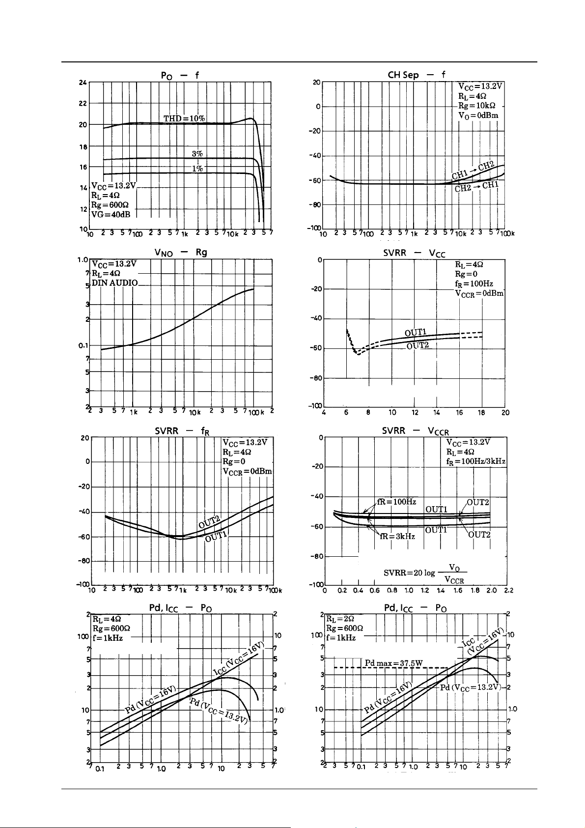
—W
O
Output power, P
Dual channel drive
— mVrms
NO
Input frequency,f—Hz
LA4708
Channel separation, CHsep — dB
Input frequency,f—Hz
Output noise voltage, V
Ripple rejection ratio, SVRR — dB
Dual channel drive
Input resistance, Rg — Ω
The value of power supply capacitor is 0.47 µF (Mylar)
Ripple frequency, f
—Hz
R
—A
CC
2200 µF
(power supply capacitor) is changed
to 0.47 µF (Mylar)
Ripple rejection ratio, SVRR — dB
Supply voltage, VCC—V
The value of power supply capacitor is 0.47 µF(Mylar)
Calculate as
Ripple rejection ratio, SVRR — dB
Power supply ripple voltage, V
Dual channel drive
Allowable power dissipation of package
CCR
— Vrms
—A
CC
Power dissipation, Pd — W
Output power, PO—W
Current drain, I
Current drain, I
Power dissipation, Pd — W
Output power, PO—W
No.5245 -7/9
Page 8
LA4708
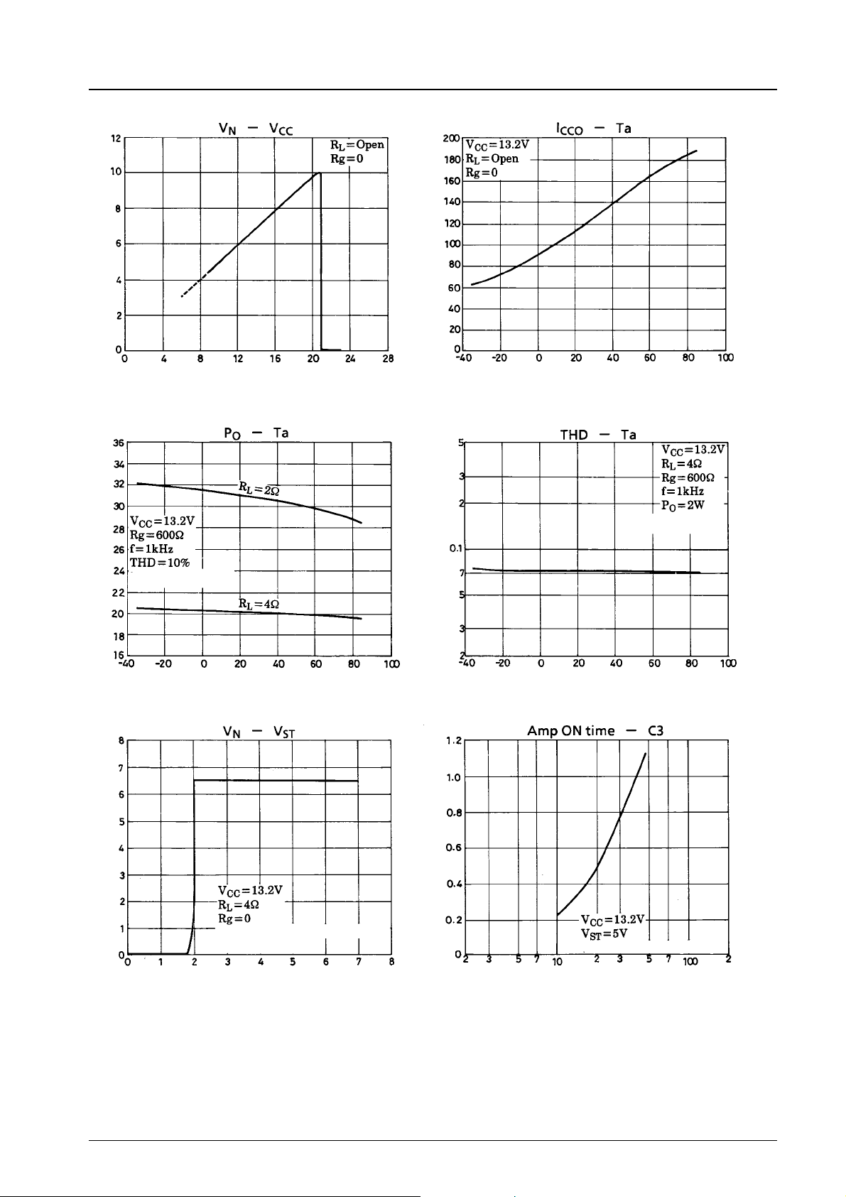
—V
N
Output pin voltage, V
—W
O
Dual channel drive
Supply voltage, VCC—V
—mA
CCO
Quiescent current, I
Ambient temperature, Ta —°C
Dual channel drive
Output power, P
—V
N
Output pin voltage, V
Ambient temperature, Ta —°C
Apply VSTto standby pin (pin 5)
through 10 kΩ.
Standby pin applied voltage, VST—V
Total harmonic distortion, THD — %
Ambient temperature, Ta —°C
Amp ON time — s
(Apply to pin 5 through 10 kΩ.)
C3—µF
No.5245 -8/9
Page 9

LA4708
No products described or contained herein are intended for use in surgical implants, life-support systems, aerospace equipment,
nuclear power control systems, vehicles, disaster/crime-prevention equipment and the like, the failure of which may directly or
indirectly cause injury, death or property loss.
Anyone purchasing any products described or contained herein for an above-mentioned use shall:
1 Accept full responsibility and indemnify and defend SANYO ELECTRIC CO., LTD., its affiliates, subsidiaries and distributors
and all their officers and employees, jointly and severally, against any and all claims and litigation and all damages, cost and
expenses associated with such use:
2 Not impose any responsibility for any fault or negligence which may be cited in any such claim or litigation on SANYO
ELECTRIC CO., LTD., its affiliates, subsidiaries and distributors or any of their officers and employees jointly or severally.
Information (including circuit diagrams and circuit parameters) herein is for example only; it is not guaranteed for volume
production. SANYO believes information herein is accurate and reliable, but noguarantees are made orimplied regarding its use
or any infringements of intellectual property rights or other rights of third parties.
This catalog provides information as of September, 1996. Specifications and information herein are subject to change without notice.
No.5245 -9/9
 Loading...