

Page 1

Any and all SANYO products described or contained herein do not have specifications that can handle
applications that require extremely high levels of reliability, such as life-support systems, aircraft’s
control systems, or other applications whose failure can be reasonably expected to result in serious
physical and/or material damage. Consult with your SANYO representative nearest you before using
any SANYO products described or contained herein in such applications.
SANYO assumes no responsibility for equipment failures that result from using products at values that
exceed, even momentarily, rated values (such as maximum ratings, operating condition ranges,or other
parameters) listed in products specifications of any and all SANYO products described or contained
herein.
Monolithic Linear IC
5.3W 2-Channel AF Power Amplifier
Ordering number:ENN1164C
LA4500
SANYO Electric Co.,Ltd. Semiconductor Company
TOKYO OFFICE Tokyo Bldg., 1-10, 1 Chome, Ueno, Taito-ku, TOKYO, 110-8534 JAPAN
Features
• Low idling current (20mA/2 channels) enabling prolonged
battery life.
• Less dependence of idling current on VCC.
• High power (5.3W typ. ×2).
• High ripple rejection (60dB at steady state).
Since filters are arranged in 3 stages (including 1 stage
inside the IC) to attain satisfactory ripple rejection at transient state, ripple occuring at the time of motor start can
be prevented from mixing in.
• Low pop noise at the time of power supply ON/OFF and
good starting balance between both channels (0.6s.) due
to built-in pop noise limiter.
• Pins provided for compensating high frequency responce.
• Low residual noise (0.4mV).
• Wide supply v oltag e range (6 to 24V) fascilitating design
of transformer power supply.
• Built-in thermal shutdown circuit,
• Designed so that inverse insertion or short between adjacent pins causes no destruction.
• Channel-to channel mirror image pin assignment and provision of Pre GND, Power GND pins enabling stable operation and fascilitating artwork of printed circuit board.
• Minimum number of external parts required (9pcs. min.,
12pcs. typ.).
• Audio muting capability (for automatic music selection,
electronic tuner).
Package Dimensions
unit:mm
3037A-DIP20H
20
8.4
R1.7
1
2.07 2.54 1.3
[LA4500]
20.0
27.0
0.6
11
11.2
12.7
10
4.04.0
SANYO : DIP20H
0.4
Specifications
Absolute Maximum Ratings at Ta = 25˚C
retemaraPlobmySsnoitidnoCsgnitaRtinU
egatlovylppusmumixaMV
tnerructuptuomumixaM
noitapissidrewopelbawollAxamdPknistaehetinifnihtiW 51W
erutarepmetgnitarepOrpoT 57+ot02–
erutarepmetegarotSgtsT 051+ot04–
xam 42V
CC
IOkaep
lennahc1 5.2A
21500TN (KT)/N2996RM/9036KI/8064KI No.1164–1/12
˚C
˚C
Page 2

LA4500
Recommended Operating Conditions at Ta = 25˚C
retemaraPlobmySsnoitidnoCsgnitaRtinU
egatlovylppuSV
ecnatsiserdaoLR
CC
L
oeretS 3
Operating Characteristics at Ta = 25˚C, VCC=12V, RL=3Ω (stereo), f=1kHz, Rg=600Ω, See specified test circuit.
retemaraPlobmySsnoitidnoC
tnerructnecseiuQI
niagegatloVGV840525Bd
ecnereffidniagegatloV
rewoptuptuOP
noitrotsidcinomrahlatoTDHTVOV2=3.05.1%
ecnatsisertupnIr
egatlovesiontuptuO
noitcejerelppiRR
noitarapeslennahCpeshck01=gR Ω mBd0=oV,5455Bd
OCC
∆ GV
O
i
VON1retlifssap-dnaB,zHk02otzH02=f,0=gR4.00.1Vm
VON2k01=gR Ω retlifssap-dnaB,zHk02otzH02=f,6.00.2Vm
r
oeretS010203Am
2,1lennahC 1±Bd
%01=DHT5.43.5W
f,0=gR
R
V,zH001=
mBd0=0506Bd
R
nimpytxam
Equivalent Circuit Block Diagram
21V
Ω
sgnitaR
03kΩ
tinU
No.1164–2/12
Page 3

Sample Application Circuit 1
LA4500
No.1164–3/12
Page 4

Description of External Parts
C1 (C1) Feedback capacitors
Related to low roll-off frequency fL for –3dB (100µF, fL=60Hz).
A capacitance value of 47µF to 100µF is recommended. Increasing the capacitance value makes the
starting time (ts) later. Decreasing the capacitance value makes the starting time (ts) earlier.
C3 (C4) Bootstrap capacitors
Decreasing the capacitance value lowers output at low frequencies. A capacitance value of 47µF to
100µF is recommended.
C5 (C6) Oscillation blocking capacitors
Polyester film capacitor, being excellent in temperature characteristic, frequency characteristics, is
recommended.
C7 (C8) Output capacitors
Related to low roll-off frequency and output at low frequencies. BTL applications normally require
output capacitors.
C9 (C10) Switching distortion compensating capacitors
Compensates switching distortion which occurs at a high frequency of 10kHz. Ceramic capacitor of
0.01µF is recommended. If no problem arises in terms of radio-casette recorder design or tone, it is
unnecessary to use these capacitors.
C11 Filter capacitor (A)
Ripple filter circuit provided in power supply line. A capacitance value of 220µF is recommended.
Ripple rejection SVRR starts to be saturated at 47µF. The starting time and pop noise generated at the
time of power supply ON must be considered when fixing the capacitance value. A capacitance value of
100µF to 220µF is usable.
C12 Filter capacitor (B)
Ripple filter circuit provided in bias circuit. A capacitance value of 100µF is recommended. 3V suffices
the breakdown voltage of this capacitor. This capacitor is for ripple rejection at transient state and rejects
noise “buzz” generated when the above-mentioned filter circuit provided in power supply line is saturated due to large ripple and supply voltage drop induced at the time of start of the motor connected to
power supply line. If the motor is satisfactory in performance and the power supply regulation including
ripple is 500mVrms or less, it is unnecessary to use this capacitor. If noise “buzz” is not offensive to the
ear, it is unnecessary to use this capacitor. In this case, other basic performances are not affected adversely.
LA4500
Feaures of IC Contents and Functions of Other Pins
(a) Since the input circuit uses PNP transistors and the bias voltage is set nearly equal to 0, no input coupling
capacitor is required, thereby enabling direct coupling. However, if slider contact noise of the variable resistor
presents any problem, connect a capacitor in series with input.
(b) Various ideas embodied in the idling circuit enable reduced I
and prolonged battery life. Since the non-
CCO
operating level of the idling circuit is made equal to that of the amplifier, crossover distortion does not worsen at
the time of reduced voltage.
(c) The open loop voltage gain is lowered and the negative feedback amount is made small to assure stable opera-
tion. Radiation to the radio-frequency stage is made less by soft clipping.
(d) Capacitors for oscillation compensation are contained as a means of reducing the number of external parts.
10pF×2 and 2pF×2 are used. Hig roll-off frequency fH (–3dB point) depends on these capacitance values.
(fH=28kHz)
(e) A thermal shutdown (THD) circuit is contained to prevent the IC from being destroyed by abromal heat genera-
tion attributable to insufficient heat dissipation. Pin (11) is used as THD control pin. Biasing pin (11) externally
makes the operating temperature lower ; and connecting a resister across pin (11) and (10) makes the operating
temperature higher. If pin (11) is connected to GND, the thermal shutdown circuit stops operating.
(f) The pin assignment is carefully considered so that no destruction takes place even if power supply is applied at a
state where adjacent pins are shorted by solder bridge, etc. Even 180°C-rotated insertion causes no destruction.
(g) Collector pins (5), (16) and base pins (6), (15) for predrive can be conveniently used in applications. For oscilla-
tion compensation occuring when operated at a lowered gain, connect a capacitor across the pins (4) and (6) and
a capacitor across pins (15) and (16). For fH compensation occuring when operated at a lowered gain, connect a
capacitor across pins (4) and (6) and a capacitor across pins (17) and (15). Further soft clippling and prevention
of waveform distortion at high frequencies are attained by connecting a series circuit of diode (DS442) and
resistor (10kΩ) across pin (6) and GND and the same across pin (15) and GND.
Continued on next page.
No.1164–4/12
Page 5
LA4500
Continued from preceding page.
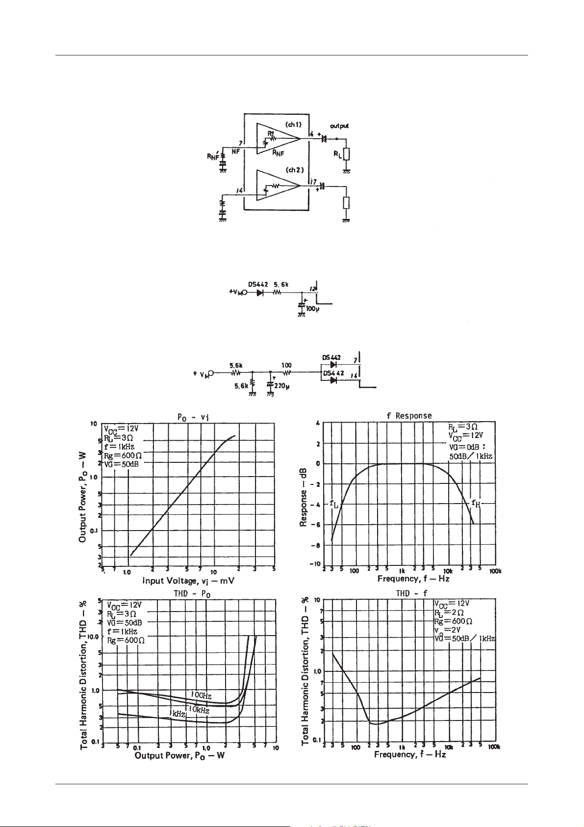
(h) Feedback resistance RNF is contained and the voltage gain is fixed at 50dB so that the variations in the voltage
gain can be minimized. The gain can be lowered by connecting RNF externally.
(i) Biasing pin (12) as shown below causes DC audio muting to be applied, thereby cutting off the IC. This makes
attack time, recovery time, pop noise, etc. saticefactory.
It is recommended that the following method be used to control the NF pin.
It is recommended that the following method be used to control the NF pin.
No.1164–5/12
Page 6
LA4500
No.1164–6/12
Page 7
LA4500
No.1164–7/12
Page 8
LA4500
No.1164–8/12
Page 9
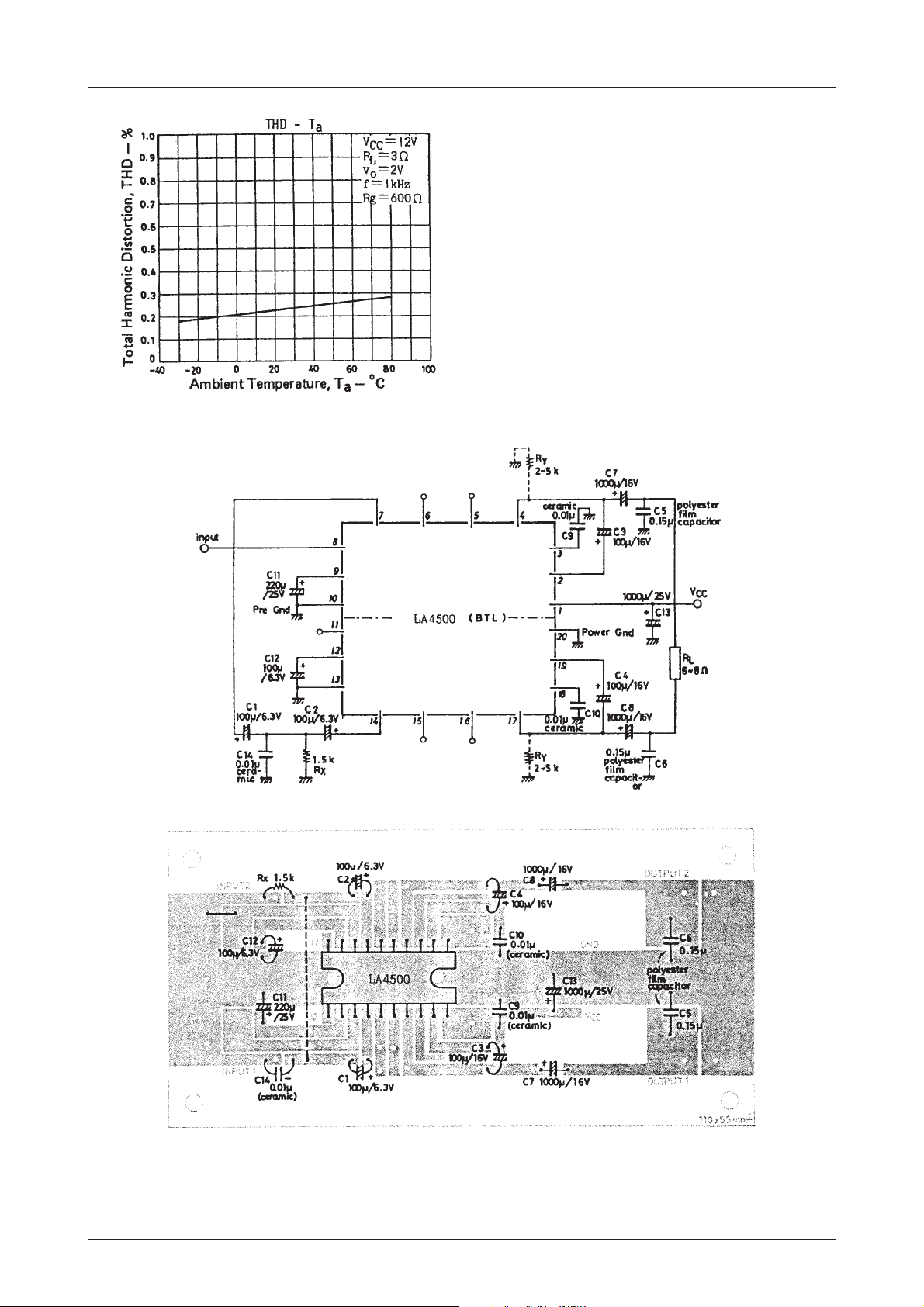
Sample Application Circuit 2
LA4500
No.1164–9/12
Page 10
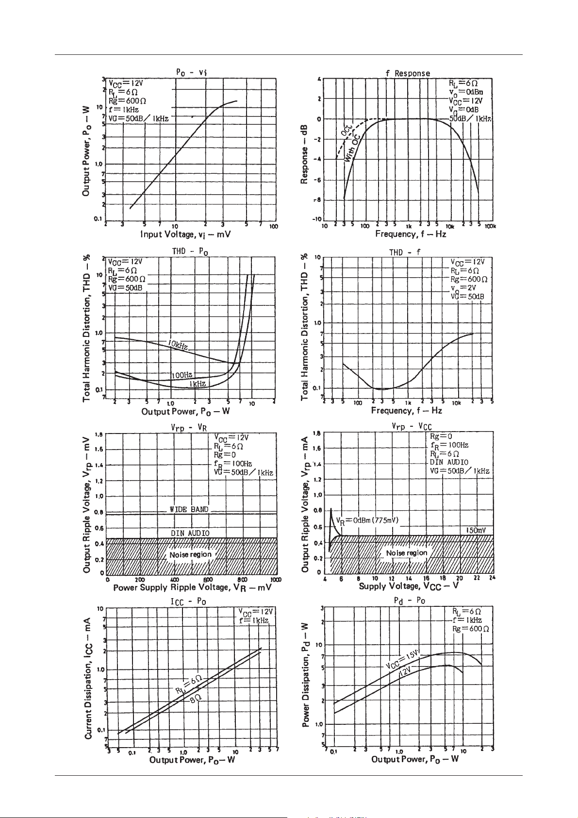
LA4500
No.1164–10/12
Page 11
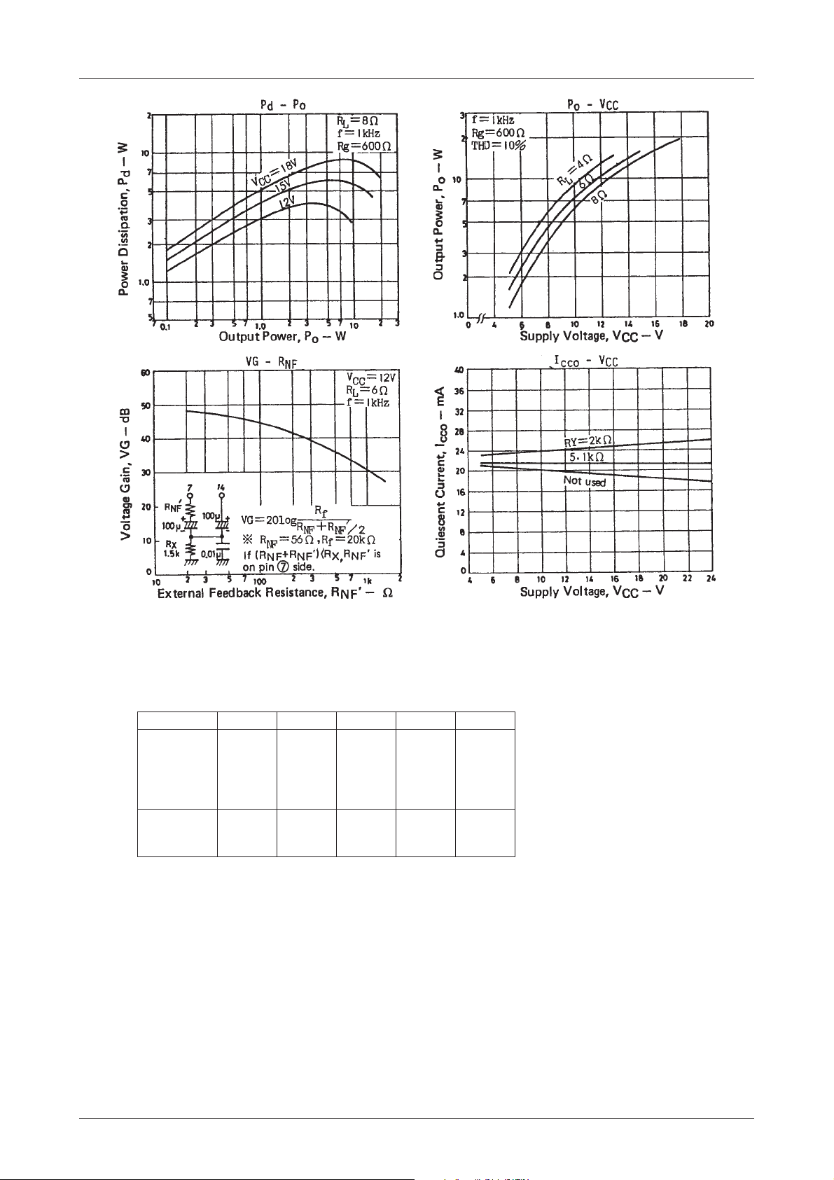
LA4500
Output power (reference value) corresponding to supply voltage and load resistance.
(THD=10%)
metsySRLV9V21V51V81
8Ω
6Ω
oeretS
egdirB
4Ω
3Ω
2Ω
8Ω
6Ω
4Ω
W4.1
W8.1
W4.2
W0.3
W5.3
W5.4
W5.5
W0.7
W5.2
W2.3
W5.4
W3.5
–
W5.8
W5.9
–
W0.4
W0.5
W9.6
W8.7
–
W31
W51
–
W6.5
W4.7
W8.9
–
–
W81
–
–
No.1164–11/12
Page 12
LA4500
Proper Cares in Using IC
· Maximum ratings
If the IC is used in the vicinity of the maximum ratings, even a slight variation in conditions may cause the maximum
ratings to be exceeded, thereby leading to breakdown. Allow an ample margin of variation for supply voltage, etc. and
use the IC in the range where the maximum ratings are not exceeded.
· Load short
If the IC is operated with the short loaded for a long time, breakdown or deterioration may take place. Be sure not to
short the load.
· Printed circuit board
When drawing the printed circuit pattern, refer to the sample printed circuit pattern. Be careful not to form a feedback
loop between input and output. Make the GND line thick and short so that no common resistance exists between Pre
GND and Power GND.
· When using the IC in radios or radio-cassette tape recorders, allow a good distance between IC and ber antenna. An
especially effectiv e measure against radiation to the SW band is to additionally connect a capacitor of 0.033µF (polyes-
ter film capacitor) across pins (2) and (20) and across pins (19) and (20) respectively.
· Normally connect the heat sink of the package to GND.
Proper Cares in Mounging Radiator Fin
1. The mounting torque is in the range of 39 to 59N · cm.
2. The distance between screw holes of the radiator fin must coincide with the distance between screw holes of the IC.
With case outline dimensions L and R referred to, the screws must be tightened with the distance between them as
close to each other as possible.
3. The screw to be used must ha v e a head equivalent to the one of truss machine screw or binder machine screw defined
by JIS. Washers must also be used to protect the IC case.
4. No foreign matter such as cutting particles shall exist between heat sink and radiator fin. When applying grease on the
junction surface, it must be applied uniformly on the whole surface.
5. IC lead pins are soldered to the printed circuit board after the radiator fin is mounted on the IC.
Specifications of any and all SANYO products described or contained herein stipulate the performance,
characteristics, and functions of the described products in the independent state, and are not guarantees
of the performance, characteristics, and functions of the described products as mounted in the customer's
products or equipment. To verify symptoms and states that cannot be evaluated in an independent device,
the customer should always evaluate and test devices mounted in the customer's products or equipment.
SANYO Electric Co., Ltd. strives to supply high-quality high-reliability products. However, any and all
semiconductor products fail with some probability. It is possible that these probabilistic failures could
give rise to accidents or events that could endanger human lives, that could give rise to smoke or fire,
or that could cause damage to other property. When designing equipment, adopt safety measures so
that these kinds of accidents or events cannot occur. Such measures include but are not limited to protective
circuits and error prevention circuits for safe design, redundant design, and structural design.
In the event that any or all SANYO products(including technical data,services) described or
contained herein are controlled under any of applicable local export control laws and regulations,
such products must not be exported without obtaining the export license from the authorities
concerned in accordance with the above law.
No part of this publication may be reproduced or transmitted in any form or by any means, electronic or
mechanical, including photocopying and recording, or any information storage or retrieval system,
or otherwise, without the prior written permission of SANYO Electric Co. , Ltd.
Any and all information described or contained herein are subject to change without notice due to
product/technology improvement, etc. When designing equipment, refer to the "Delivery Specification"
for the SANYO product that you intend to use.
Information (including circuit diagrams and circuit parameters) herein is for example only ; it is not
guaranteed for volume production. SANYO believes information herein is accurate and reliable, but
no guarantees are made or implied regarding its use or any infringements of intellectual property rights
or other rights of third parties.
This catalog provides information as of February, 2000. Specifications and information herein are subject
to change without notice.
PS No.1164–12/12
 Loading...