

Page 1

User’s Manual
DOT MATRIX PRINTER MECHANICAL
CONTROL LSI FOR DP910 SERIES
MODEL
Rev.1.00 Newly issued Sep.30th,2000
CBM-909PC SERIES
Page 2

REVISION
Rev.No. Date Content
1.00 Sep. 30, 2000 Newly issued
i
Page 3

CBM-909PC Series User’sManual
CONTENTS
1. General Specifications .................................................................................................................................................... 1
1.1 LSI Package.............................................................................................................................................................. 1
1.2 LSI Type ................................................................................................................................................................... 1
1.3 Printing functions ..................................................................................................................................................... 1
1.4 Control functions...................................................................................................................................................... 2
1.5 Operating voltage ..................................................................................................................................................... 2
1.6 Oscillation frequency ............................................................................................................................................... 2
2. Electrical Characteristics ............................................................................................................................................... 3
2.1 Absolute maximum ratings ...................................................................................................................................... 3
2.2 Operating range ........................................................................................................................................................ 3
2.3 Characteristics of LSI............................................................................................................................................... 4
2.4 Pin configurations .................................................................................................................................................... 5
3. Description of signals ...................................................................................................................................................... 8
3.1 Description of control signals .................................................................................................................................. 8
3.2 Description of communication signals .................................................................................................................. 14
3.3 Description of printer control signals .................................................................................................................... 17
3.4 Description of control functions ............................................................................................................................ 18
4. Control commands ........................................................................................................................................................ 19
4.1 Print command ....................................................................................................................................................... 19
4.2 Cancel command .................................................................................................................................................... 19
4.3 Enlarged character.................................................................................................................................................. 19
4.4 Power down control ............................................................................................................................................... 19
4.5 ESC control ............................................................................................................................................................ 23
5. Character code table ..................................................................................................................................................... 24
5.1 International character codes ................................................................................................................................. 24
5.2 Japanese character codes........................................................................................................................................ 26
ii
Page 4

CBM-909PC Series User’sManual
The CBM-909PC Series Control LSI is intended for driving the mechanism of DP910 series printer.
TYPE
CBM – 909PC – 2 D
Model name
Control LSI
Column capacity
2: 24 Columns
4: 40 Columns
Type of package
D: DIP type
F: Flat type
iii
Page 5
1. GENERAL SPECIFICATIONS
1.1 LSI Package
1) D type: 42 pin plastic Shrink DIP
2) F type: 44 pin plastic QFP
1.2 LSI Type
C-MOS LSI
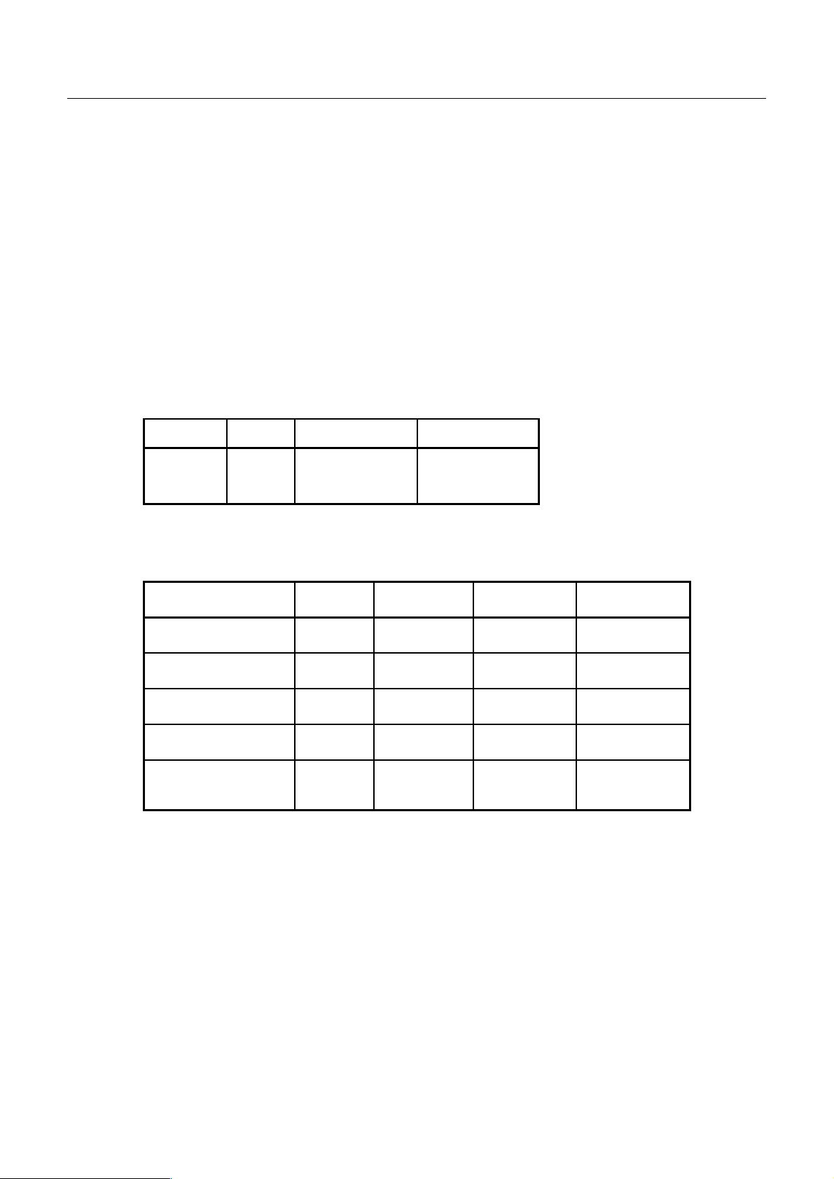
1.3 Printing Functions
Mechanism of the DP-910 series
1) Printing system: Mechanical dot matrix
2) Printer specifications:
Model Digits Printing Speed Control Board
MD-910 24 2.5 l/S CBM-909-2XX
MD-911 40 1.8 l/S CBM-909-4XX
CBM-909PC Series User’sManual
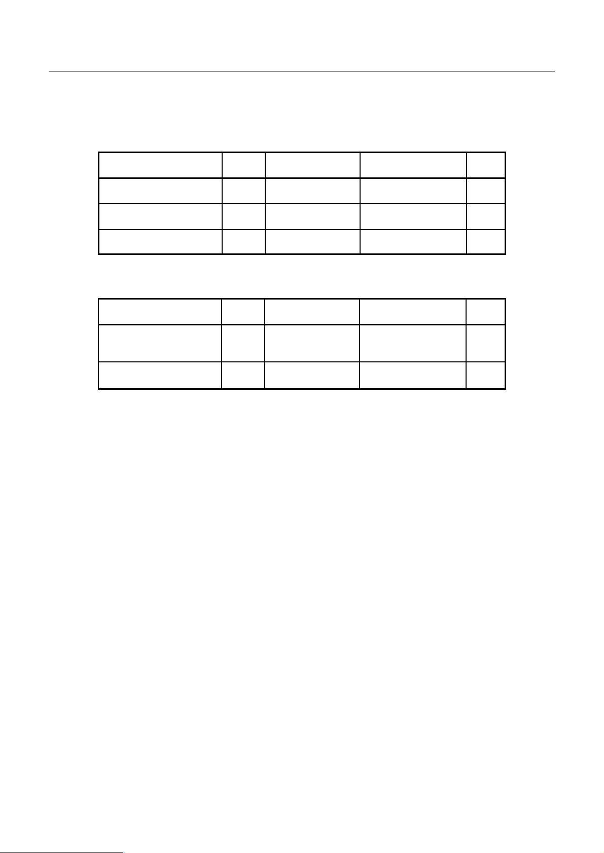
3) Types of characters
Japanese International 24 Digits 40 Digits
JIS 128 CH. V 5 x 8 dots 7 x 8 dots
ASCII (C) 64 CH. V 5 x 8 dots 7 x 8 dots
ASCII ($) 32 CH. VV5 x 8 dots 7 x 8 dots
Graphic 32 CH. VV6 x 8 dots 7 x 8 dots
Ext. char. registration
8 CH VV6 x 8 dots 7 x 8 dots
* Half dot included.
4) Line space: 2 dots, 1/36 inch (at initial setting)
5) Printing direction: L-type/R-type selectable
L-type=From the left to the right, R-type=From the right to the left
6) Bit image printing: The data subsequent to a bit image command is printed in the bit image mode.
*
1
Page 6

1.4 Control functions
1) Paper feed function
2) Self printing function
3) Buffer-full automatic printing function
4) Emergency stop function
5) Control codes
Print command: CR or LF
Input data cancel: CAN
Enlarged character printing: Double (transverse direction)
International character printing: 32 characters
Bit image printing: ESC + K + n1 + n2 + n3
CBM-909PC Series User’sManual
External character registration function: 8 characters at maximum
Line space seetting: Even number of lines out of 4 to 255 dot lines
Power-down function: DC2, DC3
Paper feed command: (ESC + B + n, 4 ≤ n ≤ 255)
1.5 Operating Voltage
1) Voltage: VDD=4.5 to 6.0 V DC at operating
VDD=3.5 to 6.0 V DC at low speed mode.*1
*1 The LSI is operated at low speed mode for first 60 ms after resetting the system.
2) Current:
VDD=5.0 V
At operating : 2.5 mA (typ.)
At power-down : DC2 0.5 mA (typ.)
At power-down : DC3 0.5 uA (typ.)
1.6 Oscillation frequency
4.19 MHz ±0.5%
2
Page 7
2. Electrical Characteristics
2.1 Absolute maximum ratings (Ta=25°C)
Item Symbol Test condition Ratings Unit
Power Supply VDD Ta = 25˚C –0.3~7.0 V
Input Voltage *1 Vi Ta = 25˚C –0.3~VDD+0.3 V
Storage temperature Tstg. — –65~150 ˚C
2.2 Operating Range
Item Symbol Test condition Ratings Unit
Power Supply VDD Operating 4.5~6.0 V
CBM-909PC Series User’sManual
low speed mode 3.5~6.0 *2 V
Operating temperature Top — –40~85 ˚C
Note)
*1. If the input voltage exceeds a rated value, malfunctioning results, and in the worst case, the IC may be destroyed.
At power-on time, do not apply an input signal prior to VDD.
*2 Under regular operations it will operate in the high speed mode between the range of 4.5-6.0 V
Before moving on to the normal operations after the power down or power on function, it will operate in low
speed between the 60 ms and operates between 3.5 and 6.0 V.
Ensure that an input signal is not input before the VDD when turning on the power. If the input signal should
come first, then add an electric current limited resistance (1k-ohm) in the series with the input ports.
3
Page 8

2.3 Characteristics of LSI
Item Sym. Test condition MIN Typ MAX Unit
“H” Input Voltage VIH
“L” Input Voltage VIL
“H” Output Voltage VOH
“L” Output Voltage VOL
Port
VDD =
4.5
~
6.0 V
CBM-909PC Series User’sManual
(Ta=–40~85°C, VDD=3.5~6.0 V)
Port 0.8 VDD VDD
V
x1, x2 VDD –0.5 VDD
Port 0 0.2 VDD
V
x1, x2 0 0.4
IOH = –1 mA VDD –1.0
V
IOH = –100 µA VDD –0.5
IOL = 1.6 mA 0.4
V
IOL = 400 µA 0.5
“H” Input Leakage Current
“L” Input Leakage Current
“H” Output Leakage Current
“H” Output Leakage Current
Built-in pull-up Resistance *2
Current
ILIH Port. VIN = VDD 3 µA
ILIL Port. VIN = 0 V –3 µA
ILOH Port. VOUT = VDD 3 µA
ILOL Port. VOUT = 0 V –3 µA
RL
IDD
*1
VDD = 5.0V
± 10%
Port
VDD = 3.0V
± 10%
f = 4.19 MHz
VDD = 5.0V ± 10%
At operating
Halt mode
VDD = 5.0V ± 10%
Stop mode
15 40 80
kΩ
30 300
2.5 8.0 mA
500 1500 µA
0.5 20 µA
Note)
*1. The IDD current is not included the current through the built-in pull-up resistance.
*2. At operating, the pull-up resistance in ports P10~P13, P20~P23, P30~P33, P60~P63, P70~P73 and P80~P81, will be
set.
At power-down mode, the pull-up resistance in ports P20~P23, P30~P33, P60~P63 and P70~P73 will be set.
Ports P40~P43, and P50~P53 are not built in pull-up resistance.
4
Page 9
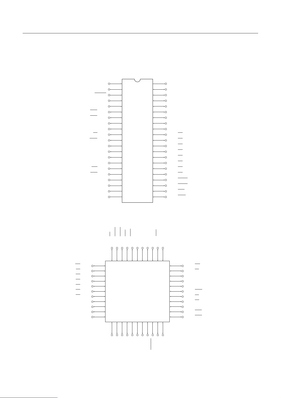
2.4 Pin configurations (Top View)
a) 42 Pin plastic shrink DIP
CBM-909PC Series User’sManual
b) 44 Pin plastic QFP
RDY
ACK
S3
RP
PF
SLIN
PXD
S2
S1
ES
INT
STB
RXD
DP
XT1
XT2
RESET
X1
X2
P33
P32
P31
P30
P81
P80
P03
P02
P01
P00
P13
P12
P11
P10
NC
V
1
2
3
4
5
6
7
8
9
10
11
12
13
14
15
16
17
18
19
20
DD
21
42
41
40
39
38
37
36
35
34
33
32
31
30
29
28
27
26
25
24
23
22
Vss
P40
P41
P42
P43
P50
P51
P52
P53
P60
P61
P62
P63
P70
P71
P72
P73
P20
P21
P22
P23
DB0
DB1
DB2
DB3
DB4
DB5
DB6
DB7
HA
HB
HC
HD
HE
HF
HG
HH
MSTR
MSTP
PFS
PWC
HG
HF
HE
HD
HC
HB
HA
DB7
DB6
DB5
DB4
P72
P71
P70
P63
P62
P61
P60
P53
P52
P51
P50
10
11
HH
MSTR
MSTP
PWC
PFS
P73
P20
P21
P23
P22
1
2
3
4
5
6
7
8
9
NC
P43
P42
P40
P41
DB3
DB2
DB0
DB1
DP
RXD
STB
DD
V
NC
P10
P11
P12
NC
3435363738394041424344
33
32
31
30
29
28
27
26
25
24
23
2221201918171615141312
SS
V
XT1
XT2
X1
RESET
X2
P13
P00
P01
P02
P03
P80
P81
P30
P31
P32
P33
INT
ES
S1
S2
RXD
SLIN
PF
RP
S3
ACK
RDY
5
Page 10

c) Pin Assignment
Pin No. Symbol Signal
QFP DIP IN OUT
CBM-909PC Series User’sManual
Function
18 1 XT1
19 2 XT2
20 3 Reset V
21 4 X1 V
22 5 X2 V
23 6 RDY V
24 7 ACK V
25 8 S3 V
26 9 RP V
27 10 RF V
Connect to VDD or VSS.
Not use
System reset signal. If this signal is set to the Low level, the inside of the
LSI is initialized.
Oscillator terminals. 4.19 MHz ± 0.5%
If receivable at data transfer time, this signal is set to the Low level.
If data read is completed at parallel data receive time, the Low pulse is
output.
Function selection S3.
RP Signal from the printer.
Paper feed signal. Effective only in the off-line mode.
28 11 SLIN V
29 12 RXD V
30 13 S2 VV
31 14 S1 VV
32 15 ES V
33 16 INT V
35 17 STB V
36 18 RXD V
On-line setting signal. When this signal is at the Low level, the on-line
mode is selected to enable data transfer. When this signal is at the High
level, the off-line mode is selected to disable data transfer.
Serial transfer. Serial data input pin.
Function selection S2 * 1
Function selection S1 * 1
Power-down command signal. If this signal is set to the Low level, control
is interrupted and oscillation stops, resulting in the power-down mode.
Power-down reset signal. If this signal is set to the Low level, the powerdown mode is reset.
Strobe pulse input
Negative logic
“Low”=8-bit data read
DIP type: Connect to 12 PIN
QFP type: Connect to 29 PIN
37 19 DP V
DP signal from the printer
6
Page 11

Pin No. Symbol Signal
QFP DIP IN OUT
CBM-909PC Series User’sManual
Function
38 20
39 21 VDD
40 22 PWC V
41 23 PFS V
42 24 MSTP V
43 25 MSTR V
44 26 HH V
127 HG V
228 HF V
329 HE V
430 HD V
531 HC V
NC
Power
The DC-DC converter control signal.
PF Solenoid signal.
Motor brake signal.
Motor drive signal.
Print solenoid drive signals.
632 HB V
733 HA V
8 34 DB7 V
9 35 DB6 V
10 36 DB5 V
11 37 DB4 V
13 38 DB3 V
14 39 DB2 V
15 40 DB1 V
16 41 DB0 V
17 42 VSS
12
Parallel data (8 bits)
Positive logic
“High”=“1”
”Low”=“0”
GND
NC
34
7
Page 12

3. Description of signals
3.1 Description of control signals
1. RESET
The LSI is initialized by setting the reset pin at the low level. The reset pulse is required to be 10 µS or more,
while the LSI is operating. When the power is switched on, if using the ceramic oscillator, send the low level
signal for 4 ms through the reset pin.
However, unless oscillation is stabilized, it is necessary to set the reset pin to the low level. After oscillation
is stabilized, set the reset pin to the high level.
VDD
PWC
CBM-909PC Series User’sManual
Reset
Oscillation
Low speed
1 Wait mode
Approx. 31.3 ms Approx. 60 ms
It is necessary to secure an oscillation stabilization time (4 ms or more).
1
mode
High speed
operation
8
Page 13

Resetting the stop mode
DC3 code
CBM-909PC Series User’sManual
Reset
PWC
Operating
Oscillation
*2) At low speed mode, power source range of 3.5~6.0 V, activate the DC-DC converter with the PWC signal
and supply the LSI with a voltage between 4.5~6.0 V.
As a result, you will obtain the operation voltage range between 3.5~6.0 V.
Resetting the halt mode
1
2
HALT HALT
Stop mode Wait mode Low speed mode
Approx. 31.3 ms Approx. 60 ms
Operating High
speed mode
RESET
PWC
Operating
Oscillation
DC2 code
HALT mode Wait mode
Low speed mode High speed mode
Approx. 31.3 ms Approx. 60 ms
9
Page 14

CBM-909PC Series User’sManual
2. PWC
This terminal will be in the “LOW” level under the low-speed operation mode (60 ms) and normal operation
mode. It will be in the “HIGH” level during power down.
By controlling (Refer to the circuitry diagram on p. XX, item XX) the DC-DC converter with the PWC signal, an
operation voltage range between 3.5-6.0 V can be obtained.
3. SLIN
Setting the SLIN pin to the Low level places this system in the on-line mode and causes it to be ready to receive
the data.
When this SLIN is at the High level, the system is placed in the off-line mode and can not receive the data. At this
time, it receives the signal PF (paper feed).
This system samples the SLIN signal in the following cases.
• After completing a system reset
• After resetting the power-down mode
• While the data is ready
• While the paper is being fed
V When the SLIN signal is set to Low during paper feed by the PF signal, the system is placed in the on-line
mode after ocmpleting that feed.
V When the SLIN signal is set to High during the text mode, the system is placed in the off-line mode after
printing the data in the print buffer.
V When the SLIN signal is set to High during the bit image mode, the data in the print buffer is cleared and the
bit image mode is also reset.
4. PF
This is a manual paper feed pin and doubles as a self test printing pin.
This pin accepts a signal only when the system is in the off-line mode, except the power-down mode.
Line feed is performed while this pin is held at the Low level (30 ms or more). To conduct a self printing test, set
the PF pin to the Low level and turn on the power or input the RESET signal.
5. INT
This is used to reset the power-down mode by the DC2 and DC3 command.
V Resetting the power-down mode by the DC2 command.
This is done by setting the INT pin to the Low level for 10 µs or more.
V Resetting the power-down mode by the DC3 command.
This is done by holding the INT pin at the Low level until XTAL oscillation is stabilized, and then, by setting
the pin to the High level.
6. ES
Setting this pin to the Low level interrupts system control and stops oscillation, resulting in the power-down
mode.
Resetting the power-down mode by the ES signal. This is done by holding the ES pin at the high level and
inputting the RESET signal.
10
Page 15

CBM-909PC Series User’sManual
7. S1, S2, S3
Function Setting DIP switch.
Symbol Function OFF ON
S1 Data transfer method Serial Parallel
S2 Printing method L-type R-type
Print command at parallel CR LF
S3
Baud rate at serial 9,600 bps 4,800 bps
1) The S1 and S2 terminals will be used as an input-port at initializing and an output-port at normally operating.
Therefore add a resistance (10 kΩ~47 kΩ) between the S1, S2 terminals and the DIP switch, and then add a
pull-up resistance (100 kΩ~150 kΩ) as shown below.
22
LS1
P23
S1
S2
S3
PWC
P01
P02
P03
14
13
3
R21
R20
47K x 2
150K x 2
VDD
DSW1
1
2
3
11
Page 16

2) Printing method
Printing method is specified by setting DIP switch S2.
For bit image printing, inverted printing is not performed even if R-TYPE is specified.
L–TYPE R–TYPE
CITIZEN
CITIZEN
CBM-909PC Series User’sManual
Paper
advance
123
123456
CBM
Paper
advance
CITIZEN
CITIZEN
CBM
123456
123
Printing direction Printing direction
12
Page 17

8. X1, X2
Use a ceramic oscillator for the clock of this LSI.
The oscillation frequency must be range 4.19 MHz ± 0.5%.
Recommended oscillator parts are the following.
CBM-909PC Series User’sManual
Maker Type f
MURATA
M.F.G
CSA 4.19 MGU
4.19 MHz ± 0.5%
CSA 4.19 MG
C1
C2
Capacitor
C1 C2
Operating
Voltage
30PF 30PF 2.7 ~ 6.0 V
30PF 30PF 3.0 ~ 6.0 V
X1
X2
CSA4.19MG
4.19MHz
9. Others
XT1 and XT2 are the input terminals when using an external clock. However, this LSI is set to use X1 and X2.
Please refrain from using terminal XT2 and connect terminal XT1 to Vss (GND).
The connect terminal NC is not connected to the inside of the LSI.
13
Page 18

3.2 Description of communication signals
1. DB0~DB7
These are parallel 8 bit data receive pins. For more details on the timing of the parallel data reception, refer to
the time chart 3.2-6.
When the SLIN is setting the low level and the RDY outputs low level, the 8 bit data is latched by the STB
signal (low level).
However, until the ACK pulse is output, hold the STB to low level.
2. RXD
This is the input pin to receive the serial data.
Refer to the timing chart 3.2-7.
When the RDY terminal is in the “LOW” level during the on-line status, the serial data from the host
computer can be received via this terminal.
This incorporates a data buffer for one line.
CBM-909PC Series User’sManual
Every time a line is printed the motor will stop, however when data transmission of the next line is finished
while the printing head is returning it can undergo continuous printing without stopping the motor.
3. RDY
This terminal is used for parallel and serial data receptions.
The signals received when the RDY signal is on-line notifies the host that the LSI data can be received.
When Using With a Parallel Interface
After verifying that the RDY signal of the host is in the ”LOW” level, there is a need to output data DB0DB7 and output the STB terminal in “LOW” level.
This LSI will maintain the RDY signal at the “HIGH” level after verifying that the STB terminal is in
“LOW” level.
However, the data read-in is not completed at this time. The data read-in of the LSI is completed only when
an ACK pulse is output.
When Using With a Serial Interface
After verifying that the RDY signal of the host side is in “LOW” level, there is a need to put the RXD signals
in the “LOW” level to perform data communication immediately after.
The RDY terminal is in the “HIGH” level under the following conditions.
a) during power down
b) during off-line
c) during data read-in
d) during printing
What is more, the RDY terminal during system reset will be in the floating status.
14
Page 19

CBM-909PC Series User’sManual
4. STB
This is a terminal used during parallel data reception and to input the data set signals from the host.
For the LSI to output signal level of this terminal it must be in the on-line status and the RDY signal must be in
the “LOW” level. If the STB terminal is in ”LOW” level, the LSI will consider that the data is sent from the host
via the DB0-DB7 and start reading the data after the RDY terminal is switched to the “HIGH” level.
When the LSI completes the data read-in it will output an ACK pulse.
There is a need to keep the STB terminal in the “LOW” level until the startup of the ACK signal at the host is
verified.
5. ACK
This is the data read-in signal used during parallel data reception.
During parallel data reception this terminal is in the on-line status and after outputting the RDY signal it will
verify that the STB terminal is in the “LOW” level.
Then it will output a “LOW” pulse of about 2 µs as a read-in timing signal to input the data in the terminal.
Therefore, there is a need for the data to be stable between, before and after these pulses.
6. Parallel interface timing chart
VDD
RESET
SLIN
RDY
DS0~DDS7
STB
ACK
RF
*1
*2 100 ms (Min.)
*5
*3
1us (Min.) 1us (Min.)
2.0us
90us (Min.)
50us (Min.)
30ms (Min.)
IN
*4
IN
50us (Max.)
OUT
IN
IN
OUT
IN
*1 It is necessary to secure an oscillation frequency stabilization time.
*2 Time required for the LSI to make the SLIN pin sensible after resetting the system.
*3 Since the DTR signal may rise regardless of the STB signal due to printer control, it is necessary to output
the STB signal within 200 µs after checking the DTR signal.
15
Page 20

*4 After this, paper feed is enabled via the PF pin.
*5 The ACK signal is output by 1 pulse after resetting the LSI.
7. Serial interface timing chart
CBM-909PC Series User’sManual
VCC
RESET
SLIM
DTR
RXD
SAMPLING
DATA
PF
*1
*2
*6
D0 D1 D2 D3 D4 D5 D6 D7
*3 *4
*5
*1 It is necessary to secure an oscillation frequency stabilization time.
*2 Time required for the LSI to make the SLIN pin sensible after resetting the system.
*3 The number of start bits should be 1 bit.
*4 The number of stop bits should be 1 bit or more.
IN
IN
50us (Max.)
OUT
IN
IN
30ms (Min.)
*5 After this, paper feed is enabled via the PF pin.
*6 The DTR signal may rise regardless of the RXD signal due to printer control. When transferring the data,
therefore, it is necessary to set the RXD signal to the Low level within 200 µs after checking the DTR signal,
and then, transfer the data.
16
Page 21

3.3 Description of printer control signals
1) RP
This terminal is used to input the signal that determining the printing start position. Connect it on one side of
the reset detector on the printer.
The other terminal of the reset detector is to be connected to the GND or the PWC terminal.
2) MSTR
This is the motor drive signal terminal and the motor will operate when the terminal is in the “LOW” level
status.
3) MSTP
This is the motor control signal terminal and outputs a “LOW” level of a maxinum of 60 ms immediately
after the motor is turned off.
Brake the motor when this terminal is in the “LOW” level status.
4) HA, HB, HC, HD, HE, HF, HG, HH
CBM-909PC Series User’sManual
These terminals output the drive signals of the printer solenoid and the printer solenoid is activated when
these terminals are in the “LOW” level.
5) PFS
This is the paper feed solenoid drive signal and will drive the PF solenoid when this terminal is in the
“LOW” level.
6) DP
Received the printer solenoid drive timing from the printer.
Upon onset of the printer timing, it is advised that the DP signal from the printer is shaped with a transistor,
and then put in the LSI DP terminal since it employs a photosensor.
+V
VDD
DP
P10/Pin#19
Photo-Sensor
17
Page 22

3.4 Description of control functions
1. Buffer full automatic print
When the input buffer is filled up by the character data, it starts the printing automatically.
2. Self test printing
This LSI has a built in self print function.
Take the following procedures to test.
a) Set the paper properly.
b) Turn off the power switch.
c) Turn on the power switch while keeping the PF signal to the low level, then set it to the high level.
d) To stop the printing, turn off the power switch or set RESET signal to low level.
3. Emergency Stop Function
CBM-909PC Series User’sManual
When the following abnormalities are detected during the print operation, cut off the power to the print head
solenoids and motor, and put the LSI in the power down mode.
The emergency stop can be cleared by resetting the LSI.
Printer abnormalities are as follows.
a) Motor lock.
b) Operation defect in the timing detector (DP signal)
c) Operation defect in the reset detector (RP signal)
18
Page 23

4 CONTROL COMMANDS
4.1 Print commands: CR (0DH), LF (0AH)
When the parallel interface is used, either CR or LF code can be selected by preset (S3). If the set CR or LF code
is input, the data in the print buffer is printed and line feed is performed.
When the serial interface is used, only the CR code becomes effective regardless of preset (S3).
When graphic mosaic printing is performed, line feed is not performed by the print command, and graphic mosaic
printing is allowed on the next line.
4.2 Cancel command: CAN (18H)
This code cancels all the data on the identical line in the print buffer, which was input before the code is input.
4.3 Enlarged character printing: SO (0EH)
The printing data following this code is printed with its width doubled.
This function is cleared by the print command (CR LF) or DC4 (14H).
4.4 Power-down control: DC2 (12H), DC3 (13H)
CBM-909PC Series User’sManual
There are two kinds of power-down mode, DC2 and DC3 codes, in order to reduce current consumption. If this
code is received, the power-down mode is put into effect after printing the data received before it.
a. DC2 (12H)
Inputting the DC2 code places this unit in the power-down mode.
At this time, oscillation of the oscillator does not stop.
[Resetting the power-down mode]
a-1) Input to INT
If the Low pulse is applied to the INT pin for 10 µs or more, the condition existing just before power-
down is restored in about 100 ms and allows you to control the printer and transfer the data.
a-2) Input to RESET
If the Low pulse is applied to the RESET pin for 4 ms or more, the power-down mode is reset and the
inside of the unit is initialized to be ready to operate in about 100 ms.
b. DC3 (13H)
Inputting the DC2 code places this unit in the power-down mode.
At this time, oscillation of the oscillator stops. Therefore, current consumption is much less than the DC2
power-down mode.
[Resetting the power-down mode]
b-1) Input to INT
If the Low level is applied to the INT pin for 10 µs, the power-down mode is reset, and about 4 ms after
oscillation is stabilized, the condition existing just before power-down is restored in about 100 ms and
allows you to control the printer and transfer the data.
19
Page 24
CBM-909PC Series User’sManual
b-2) Input to RESET
If the Low level is applied to the RESET pin for 4 ms or more, the power-down mode is reset. However,
unless oscillation is stabilized, it is necessary to set the RESET pin to the Low level. After oscillation is
stabilized, set the RESET pin to the High level.
This initializes the inside of the unit and starts it in about 100 ms.
D0 through D7 are dot points in each position:
“1” for a point, and “0” for a space.
When n1, n2, n3, are specified beyond their ranges, or when n2=n3=0 is specified, the text mode results with the
bit image mode cancelled.
Since this printer prints by 4-dot line, insufficient data is printed as a space after reading in the 4-dot line worth of
data or when the n1, n2, n3, specified data is completed.
IN the MD-910 specifications, when n1,=23 is specified, the 4 dots from the most significant dot (MSC DOT) are
invalidated. This is because there are 180 dots fro one-line printing positions.
Although the text mode has been restored after bit image printing, the line space=0 has been assumed.
Therefore, it is necessary to perform line feed before printing in the text mode.
Note)
For bit image printing, inverted printing is not performed even if R-type is specified.
c. International character setting; ESC + R + n
The ESC + R + n command specifies the following character table of each country.
n Country n Country
0 U.S.A 5 Sweden
1 France 6 Italy
2 Germany 7 Spain
3 Britain 8 Japan
4 Denmark
“n” other 0 to 8 is invalid (not changed).
n=8 (Japan) is set at power-on or after a reset.
20
Page 25

CBM-909PC Series User’sManual
d. External character registration; ESC + & + A1 + A2
Up to 8-character pattern can be registered by inputting the pattern data following the ESC + & + A1 + A2
command.
Registerable character addresses are the code table 20H through OFFH, that is 8 characters.
The character address at the start of registration is “A1”, and that at the end of registration is “A2”.
When registering one character, it should be A1=A2.
When registering multiple characters, it should be A1<A2 and A2-A1 ≤ 7.
When external character registration is done in the same character address duplicately, the pattern registered later
becames effective.
If more than 8 characters are registered, all the character patterns registered so far are cleared.
The pattern data should be as follows.
The MD-910 specifications require 6 bytes per character.
1 1
23456
LSD
MSD
63H255H349H441H541H641H
Pattern data (6 bytes)
The MD-911 specifications require 7 bytes per character.
1 1
234567
LSD
MSD
41H222H355H408H541H600H741H
Pattern data (7 bytes)
The pattern for the MD-911 specifications does not allow the dots to be consecutively arranged in the printing direction
(line direction).
Printing is not allowed at the point “*” to the right of the point “.”shown above. Even if you specify the pattern at the
point “*”, the print “*” of registration is canceled.
21
Page 26

CBM-909PC Series User’sManual
e. Continuous paper feed; ESC + B + n
The ESC + B + n command provides continuous paper feed by “n” lines.
The range of “n” is even-number dot lines within 4 ≤ n ≤ 255.
When “n” is an odd number, it is assumed to be an even number of “n-1”.
When the number within the range of “0 ≤ n ≤ 3” is specified for “n”, this command is canceled.
When there is data in the buffer, this command will be carried out n-dot line feed after printing is completed.
If the range of “n” is within 4 ≤ n ≤ 9, there is no line space.
22
Page 27

CBM-909PC Series User’sManual
4.5 ESC control
The following setting funcitons can be performed by the ASCII code subsequent to the ESC (1BH) code. If you
input other ASCII code than those defined below after the ESC code, that ASCII code and the ESC code are
invalidated. In the following commands;
“n” is an 8-bit binary number.
“+” is a separator for convenience sake.
a. Line space setting command: ESC + A + n
The command ESC + A + n allows you to set the interline space of “n” dots.
“n” should be 0 ≤ n ≤ 255. If an odd number is specified for “n”, the line space will be “n-1” dots.
Initial setting for the line space is 2 dots.
b. Bit image printing: ESC + K + n1 + n2 + n3
The command ESC + K + n1 + n2 + n3 changes over the mode from the text mode to the bit image mode.
The transfer amout of the bit image data entered subsequent to this command is specified with n1, n2, n3.
D7 D6 D5 D4 D3 D2 D1 D0
n3 x 256 + n2
Ranges of n1, n2, n3
n1
1 Byte
n 1 n 2 n 3
MD – 910 1 ~ 18 0 ~ 255 0 ~ 1
MD – 911 1 ~ 23 0 ~ 255 0 ~ 1
23
Page 28

5 CHARACTER CODE TABLE
5.1 INTERNATIONAL CHARACTER CODES
CBM-909PC Series User’sManual
24
Page 29

CBM-909PC Series User’sManual
25
Page 30

5.2 JAPANESE CHARACTER CODES
CBM-909PC Series User’sManual
26
 Loading...