

PROPRIETARY NOTE
THIS SPECIFICATION IS THE PROPERTY OF BOE HF AND SHALL NOT BE
REPRODUCED OR COPIED WITHOUT THE WRITTEN PERMISSION OF BOE OT AND
MUST BE RETURNED TO BOE HF UPON ITS REQ UEST.
SPEC. NUMBER
TITLE : HT260WXC-100 Product Specification
PRODUCT GROUP
TFT-LCD
Rev. P1
REV.
P1
ISSUE DATE
2011.2.15
PAGE
1
OF 27
www.jxlcd.com
www.jxlcd.com
B2010-6011-O(1/3)
A4(210 X 297)

PRODUCT GROUP
REV
ISSUE DATE
SPEC. NUMBER
TFT- LCD PRODUCT
SPEC. TITLE
HT260WXC-100 Product Specification Rev P1
P1 2011.2.15
PAGE
OF 26
2
REVISION HISTORY
REV. ECN NO. DESCRIPTION OF CHANGES DATE PREPARED
PO Initial Release 10.12.30 金在 光
P1 量产对应 Release 11.2.15 金在 光
www.jxlcd.com
www.jxlcd.com
B2010-6011-O(2/3) A4(210 X 297)

PRODUCT GROUP
REV
ISSUE DATE
SPEC. NUMBER
No ITEM Page
1 GENERAL DESCRIPTION
2 ABSOLUTE MAXIMUM RATINGS 6
3 ELECTRICAL SPECIFICATIONS 7
TFT- LCD PRODUCT
SPEC. TITLE
HT260WXC-100 Product Specification Rev P1
P1
2011.2.17
Contents
REVISIONS HISTORY 2
CONTENTS
1.1 Introduction
1.2 Features
1.3 Applications
1.4 General Specification
PAGE
3
3
4
OF 27
4 INTERFACE CONNECTION 9
4.1 Module Input Signal & power
www.jxlcd.com
www.jxlcd.com
5 SIGNAL TIMING SPECIFICATIONS
6 OPTICAL SPECIFICATIONS 16
7 MECHANICAL CHARACTERISTICS 18
8RELIABLITY
9 PRODUCT SERIAL NUMBER 20
10 PACKING INFORMATION
11 HANDING & CAUTIONS 23
12 APPENDIX
4.2 Back-light Interface Connection
4.3 LVDS Interface
12
5.1 Timing Parameter
5.2 Signal Timing Waveform
5.3 Input Signals, Basic Display Colors & Cray Scale Of Colors
5.4 Power Sequence
19
21
24
B2010-6011-O(3/3) A4(210 X 297)
PRODUCT GROUP
REV
ISSUE DATE
SPEC. NUMBER
TFT- LCD PRODUCT
SPEC. TITLE
HT260WXC-100 Product Specification Rev P1
P1
2011.2.17
4
1.0 GENERAL DESCRIPTION
1.1 Introduction
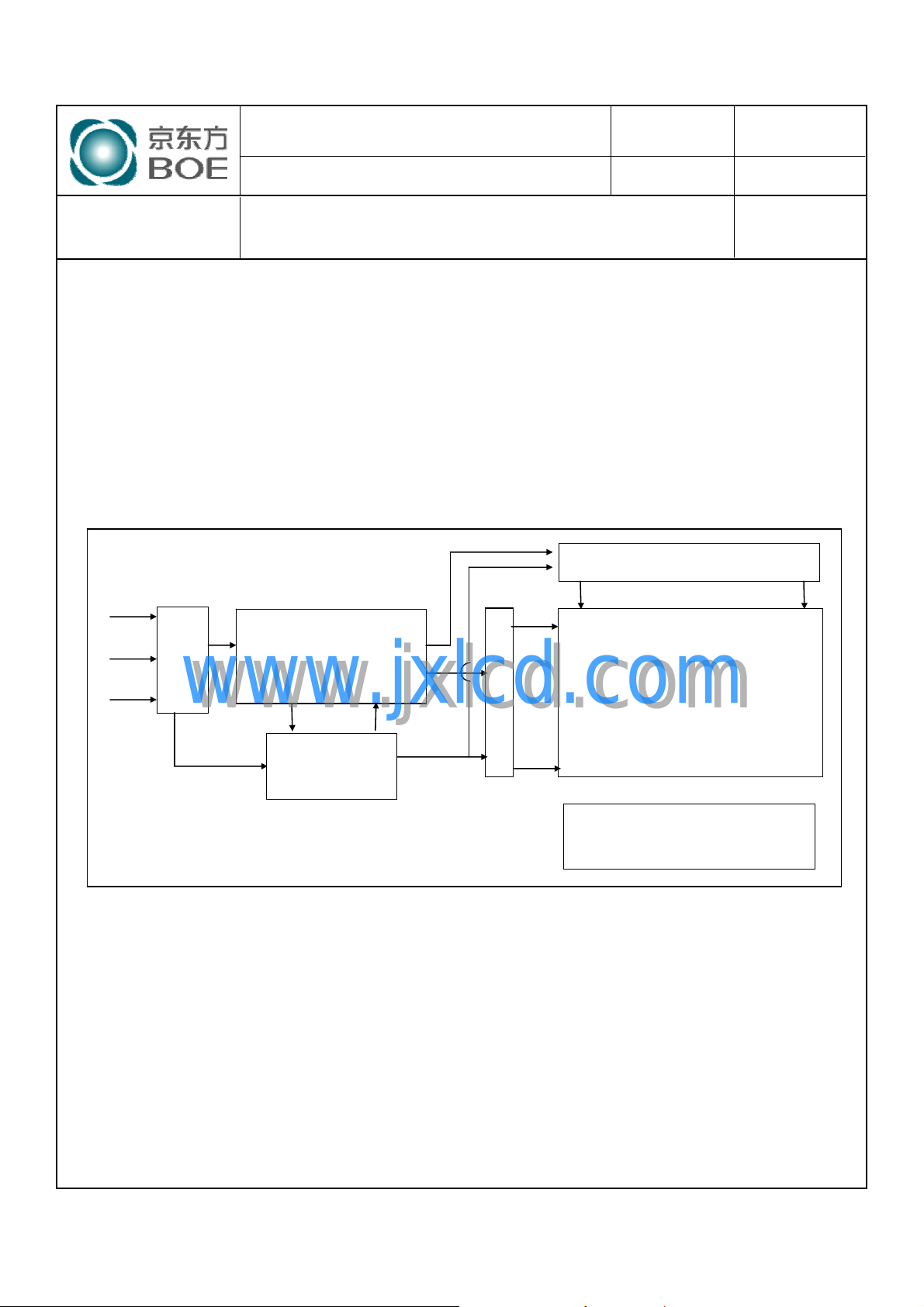
HT260WXC-100 is a color active matrix TFT LCD module using amorphous silicon TFT's
(Thin Film Transistors) as an active switching devices. This module has a 26.0inch diagonally
measured active area with WXGA resolutions (1366 horizontal by 768 vertical pixel array).
Each pixel is divided into RED, GREEN, BLUE dots which are arranged in vertical stripe and
this module can display 16.7M colors. The TFT-LCD panel used for this module is adapted for a
low reflection and higher color type.
RGB(Mini-LVDS)
Source Driver Circuit
S1 S1366
G1
+12.0V
LVDS
5pair
Option
# 9
CN1
(30pin)
www.jxlcd.com
www.jxlcd.com
Timing Controller
[LVDS Rx & Mini-LVDS
Tx integrated]
Gate Driver Circuit
TFT - LCD Panel
(1366 × RGB × 768 pixels)
PAGE
OF 27
Power Circuit
Block
G768
Back light Assembly
(4 U_CCFL)
1.2 Features
z LVDS Interface with 1 pixel / clock
z High-speed response
z Lower Color shift Image Quality
z 6-bit Hi-FRC color depth, display 16.7M colors
z High luminance and contrast ratio, low reflection and wide viewing angle
z DE (Data Enable) only mode
z RoHS Compliant
B2010-6011-O(3/3) A4(210 X 297)
PRODUCT GROUP
REV
ISSUE DATE
TFT- LCD PRODUCT
SPEC. NUMBER
1.3 Application
z Home Alone Multimedia TFT-LCD TV
z Display Terminals for Control System
z High Definition TV(HD TV)
z AV application Products
1.4 General Specification
Parameter Specification Unit Remarks
Active area 575.769(W) x 323.712(H) mm
SPEC. TITLE
HT260WXC-100 Product Specification Rev P1
< Table 1. General Specifications >
P1
2011.2.17
PAGE
OF 27
5
Number of pixels 1366(H) ×768(V) pixels
Pixel pitch 140.5(H) ×RGB×421.5(V)
www.jxlcd.com
Pixel arrangement Pixels RGB stripe arrangement
Display colors 16.7M(6bits + Hi FRC) colors
Display mode Transmission mode, Normally White
Outline Dimension 626.0(H) × 373.0(V) × 32.0(D) (typ.) mm
Weight 3700 (typ.) gram
Power Consumption Total 40.6Watt (Typ.) (Logic=2W,
Surface Treatment Haze 25%, 3H, Semi-glare treatment
www.jxlcd.com
Lamp=38.6W [IBL=7mA] )
(Front Polarizer)
㎛
Watt
B2010-6011-O(3/3) A4(210 X 297)

PRODUCT GROUP
REV
ISSUE DATE
SPEC. NUMBER
TFT- LCD PRODUCT
SPEC. TITLE
HT260WXC-100 Product Specification Rev P1
P1
2011.2.17
6
2.0 ABSOLUTE MAXIMUM RATINGS
The followings are maximum values which, if exceed, may cause faulty operation or
damage to the unit. The operational and non-operational maximum voltage and current
values are listed in Table 2.
< Table 2. LCD Module Electrical Specifications >
Parameter Symbol Min. Max. Unit Remarks
Power Supply Voltage VDD VSS-0.3 13 V Ta = 25 ℃
Back-light Lamp Current IBL 6.0 9.0 mArms
Back-light Lamp Frequency FL 40 80 KHz
Operating Temperature T
Storage Temperature T
Operating Ambient Humidity Hop 10 80 %RH
www.jxlcd.com
www.jxlcd.com
T
OP
SUR
ST
0+50
0+60
-20 +60
℃
℃
℃
[VSS=GND=0V]
1)
PAGE
OF 27
Storage Humidity Hst 10 80 %RH
Note : 1) Temperature and relative humidity range are shown in the figure below.
Wet bulb temperature should be 39 ℃ max. and no condensation of water.
80%
60
60%
Wet Bulb
Temperature [C]
30
20
10
0
10 20 30 40 50 60 70 800-20
Dry Bulb Temperature [
50
40
40%
Humidity [(%)RH]
10%
°C]
Storage
Operation
B2010-6011-O(3/3) A4(210 X 297)

PRODUCT GROUP
REV
ISSUE DATE
SPEC. NUMBER
TFT- LCD PRODUCT
SPEC. TITLE
HT260WXC-100 Product Specification Rev P1
P1
2011.2.17
PAGE
7
3.0 ELECTRICAL SPECIFICATIONS
< Table 3. LCD Module Electrical Specifications >
Parameter Symbol
Power Supply Input Voltage VDD 11.4 12 12.6 V
Power Supply Ripple Voltage VRP 300 mV
Power Supply Current IDD - 170 300 mA 1
Power Consumption of VDD PDD - 2 3.5 Watt
Rush current IRUSH - - 3.0 A 2
LVDS
Interface
Differential Input High
Threshold Voltage
Differential Input Low
Threshold Voltage
VLVTH +100 mV
VLVTL -100 mV
Min Typ Max
Values
Unit Notes
[Ta =25±2 ℃]
OF 27
Common Input Voltage VLVC 1.0 1.2 1.4 V
www.jxlcd.com
www.jxlcd.com
Input High Threshold
CMOS
Interface
Back-light Lamp Voltage VBL 1242 1380 1518 Vrms IBL=7.0 mA
Back-light Lamp Current IBL 6.5 7.0 7.5 mArms
Back-light Lamp operating
Frequency
Lamp Start Voltage Vs
Lamp Life 50,000 - - Hrs IBL=7.0mA, 5
Power Consumption of BL
Voltage
Input Low Threshold
Voltage
VIH 2.7 - 3.3 V
VIL 0 - 0.7 V
FL 40 - 80 KHz 3
- - 2200 Vrms 25℃, 4
- - 2400 Vrms 0℃, 4
PBL - 38.6 - W IBL=7.0mA, 6
B2010-6011-O(3/3) A4(210 X 297)

PRODUCT GROUP
REV
ISSUE DATE
SPEC. NUMBER
Notes :
1. The supply voltage is measured and specified at the interface connector of LCM.
The current draw and power consumption specified is for VDD=12.0V, Frame rate=60Hz
and Clock frequency = 75.4MHz. Test Pattern of power supply current
a) Typ : Black Pattern
b) Max : Sub Dot Pattern
2. The duration of rush current is about 2ms and rising time of Power Input is 1ms(min)
White : 255Gray
Black : 0Gray
Mosaic Pattern(8 x 6)
TFT- LCD PRODUCT
SPEC. TITLE
HT260WXC-100 Product Specification Rev P1
P1
2011.2.17
PAGE
OF 27
8
www.jxlcd.com
www.jxlcd.com
3. The frequency range can be keep within ±10% range of electrical and optical
characteristics. (except the chromaticity)
4. Output voltage of test circuit in order to stabilize discharge in tube. Lamp and
test circuit should be left at the above standard conditions over 1Hr.
5. The lifetime is judged to be over when any situation mentioned below occurs:
・When the central lamp luminance decline to 50% of the initial luminance.
・When the lamp starting voltage is 10% higher than its specification
6. Calculated value for reference (VBL × IBL) ×4 excluding inverter loss
B2010-6011-O(3/3) A4(210 X 297)

PRODUCT GROUP
REV
ISSUE DATE
SPEC. NUMBER
TFT- LCD PRODUCT
SPEC. TITLE
HT260WXC-100 Product Specification Rev P1
P1
4.0 INTERFACE CONNECTION
4.1 Module Input Signal & Power
- Connector : IS100-L30B-C23(Manufactured by UJU) or Equivalent.
< Table 4. LCM Module Input Connector Pin Configuration >
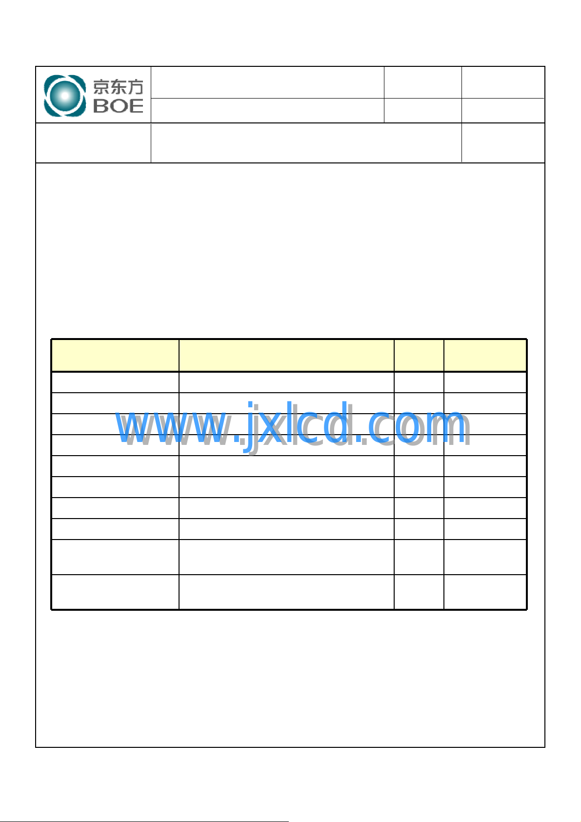
Pin No Symbol Description Pin No Symbol Description
1 VDD Power Supply +12.0V 16 RX1+ LVDS Receiver Signal(+)
2 VDD Power Supply +12.0V 17 GND Ground
3 VDD Power Supply +12.0V 18 RX2- LVD S Recei ver Si g nal (-)
4 VDD Power Supply +12.0V 19 RX2+ LVDS Receiver Signal(+)
5 GND Ground 20 GND Ground
6 GND Ground 21 RCLK- LVDS Receiver Clock Signal(-)
7 GND Ground 22 RCLK+ LVDS Receiver Clock Signal(+)
8 GND Ground 23 GND Ground
9 LVDS_SEL ‘L’=JEIDA , ‘H’or NC= VESA 24 RX3- LVDS Receiver Signal(-)
10 NC No Connection 25 RX3+ LVDS Receiver Signal(+)
11 GND Ground 26 GND Ground
12 RX0- LVDS Receiver Signal(-) 27 NC No Connection
13 RX0+ LV DS Receiver Signal(+) 28 NC No Connectio n
14 GND Ground 29 GND Ground
15 RX1- LVDS Receiver Signal(-) 30 GND Ground
www.jxlcd.com
www.jxlcd.com
2011.2.17
PAGE
OF 27
9
Notes : 1. NC(Not Connected) : This pins are only used for BOE internal operations.
2. Input Level of LVDS signal is based on the IEA 664 Standard.
3. LVDS_SEL : This pin is used for selecting LVDS signal data format.
If this Pin : High (3.3V) or Open (NC) Æ Normal NS LVDS format
Otherwise : Low (GND) Æ JEIDA LVDS format
Sequence : On = Vdd ≥LVDS Option ≥Interface signal
Off = Interface signal ≥LVDS Option ≥ Vdd
Rear view of LCM
1
B2010-6011-O(3/3) A4(210 X 297)
IS100-L30B-C23 (UJU)
30
 Loading...