

Page 1
PROPRIETARY NOTE
THIS SPECIFICATION IS THE PROPERTY OF BOE HYDI S AND SHA LL NOT BE
REPRODUCED OR COPIED WITHOUT THE WRITTEN PERMISSION OF BOE
HYDIS AND MUST BE RETURNED TO BOE HYDIS UPON ITS REQUEST
TITLE : HV150UX1-100
Product Specification for Lenovo
Rev. A
www.jxlcd.com
www.jxlcd.com
BEIJING BOE OPTOELECTRONICS TECHNOLOGY
SPEC. NUMBER
BOE TFT-LCD SBU
BOE HYDIS TECHNOLOGY
PRODUCT GROUP
REV.
ISSUE DATE
PAGE
S864-1236 1
B2005-C001-O (1/3) A4(210 X 297) A4(210 X 297)
TFT LCD
A
2005.12.20
OF 30
Page 2

PRODUCT GROUP
REVISION HISTORY
ISSUE DATEREV
2005.12.20ATFT LCD PRODUCT
PREPARED DATE DESCRIPTION OF CHANGES ECN NO.REV.
S.H.YUN05.08.22Initial Release0
A
E0511-F021
www.jxlcd.com
www.jxlcd.com
S.H.YUN05.12.201. Add a max power value and current
2. Change the tolerance of white
chromaticity
3. Add a Lenovo barcode in Product label
4. Change the outline drawing of rear view
5. Apply new EDID data
SPEC. NUMBER
S864-1236 2
B2003-002-B(2/3) A4(210 X 297)
SPEC TITLE
HV150UX1-100 Product Specification for Lenovo
PAGE
OF 30
Page 3
PRODUCT GROUP
Contents
ISSUE DATEREV
2005.12.20ATFT LCD PRODUCT
PageItemNo
4General Description1.0
6Absolute Maximum ratings2.0
7Electrical specifications.3.0
9Optical specifications.4.0
13Interface Connection5.0
16Signal Timing Specification6.0
www.jxlcd.com
www.jxlcd.com
16Signal Timing waveforms7.0
18Input Signals, Display Colors & Gray Scale of Colors8.0
19Power Sequence9.0
20Mechanical Characteristics10.0
21Reliability Test11.0
22Handling & Cautions.12.0
23Packing information13.0
24Label14.0
26EDID data table 15.0
29Outline drawing (Front and Rear)Appendix
SPEC. NUMBER
S864-1236 3
B2005-C001-O(3/3) A4(210 X 297)
SPEC TITLE
HV150UX1-100 Product Specification for Lenovo
PAGE
OF 30
Page 4
PRODUCT GROUP
ISSUE DATEREV
2005.12.20ATFT LCD PRODUCT
1.0 GENERAL DESCRIPTION
1.1 Introduction
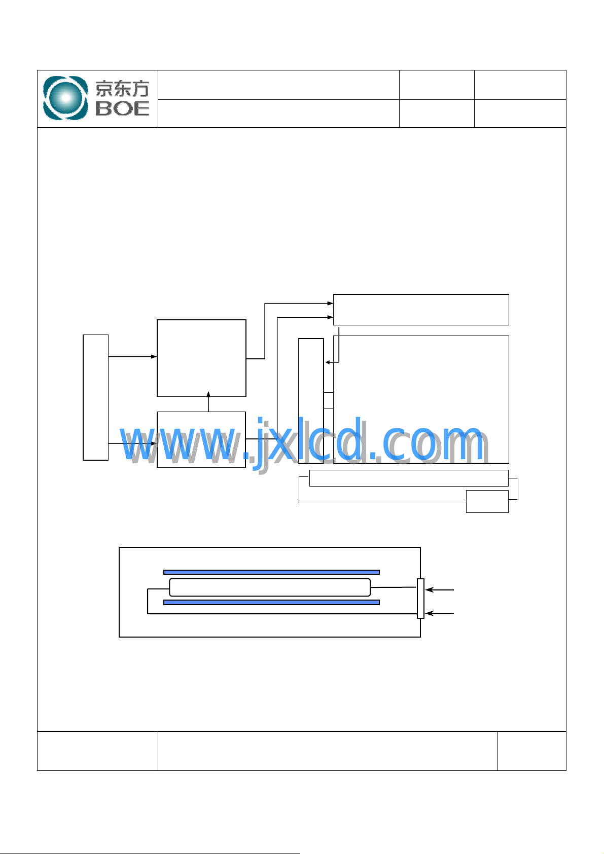
HV150UX1-100 is a color active matrix TFT LCD module using amorphous silicon TFT's
(Thin Film Transistors) as an active switching devices. This module has a 15.0 inch
diagonally measured active area with UXGA resolutions (1600 horizontal by 1200 vertical
pixel array). Each pixel is divided into RED, GREEN, BLUE dots which are arranged in
vertical stripe and this module can display 262,144 colors. The TFT-LCD panel used for this
module is a low reflection and higher color type. Therefore, this module is suitable for
Notebook PC. The DC/AC inverter for back-light driving is not built in this model.
Source Driver
Connector (CN )
LVDS
Input
Signal
LVDS Rx
+
T/CON
Gate Driver
TFT LCD Panel
BACK LIGHT (Fluorescent Lamp)
1600 ×1200
1
VDD
www.jxlcd.com
www.jxlcd.com
DC/DC
Gamma
Vcom
Reflector
LAMP
HOT (Pink)
1
CN2
COLD (Black)
2
Note) The output of the inverter may change according to the material of the
reflector.
SPEC. NUMBER
S864-1236 4
B2005-C001-O(3/3) A4(210 X 297)
SPEC TITLE
HV150UX1-100 Product Specification for Lenovo
PAGE
OF 30
Page 5

PRODUCT GROUP
1.2 Features
z 15.0 UXGA FFS
z Thin and light weight
z 3.3 V power supply
z 2 Channel LVDS Interface
z Single CCFL (Bottom side/Horizontal Direction)
z 262,144 colors
z Data enable signal mode
z Side Mounting Frame
z Green Product (RoHS)
z On Board EDID chip
z High contrast ratio
1.3 General Specification
The followings are general specifications at the model HV150UX1-100. (listed in Table 1.)
<Table 1. General Specifications>
ISSUE DATEREV
2005.12.20ATFT LCD PRODUCT
www.jxlcd.com
www.jxlcd.com
Dimensional outline
Power consumption
RGB Vertical stripePixel arrangement
Normally BlackDisplay mode
317.3±0.5(H) ×242.0±0.5(V) ×6.5(D:max)
AG(H45%)/AR/2HSurface treatment
: 6.1
total
RemarksUnitSpecificationParameter
mm304.8 (H) ×228.6 (V) (15.0” diagonal)Active area
pixels1600(H) ×1200(V)Number of pixels
mm0.1905(H) ×0.1905(V)Pixel pitch
colors262,144Display colors
mm
g540 g (typ.)Weight
Note 1Bottom edge side, 1-CCFL typeBack-light
WPD: 2.0
WPBL: 4.1
WP
Note 1: CCFL (Cold Cathode Fluorescent Lamp)
SPEC. NUMBER
S864-1236 5
B2005-C001-O(3/3) A4(210 X 297)
SPEC TITLE
HV150UX1-100 Product Specification for Lenovo
PAGE
OF 30
Page 6

PRODUCT GROUP
ISSUE DATEREV
2.0 ABSOLUTE MAXIMUM RATINGS
The followings are maximum values which, if exceed, may cause faulty operation or
damage to the unit. The operational and non-operational maximum voltage and current
values are listed in Table 2.
< Table 2. Absolute Maximum Ratings>
Ta=25+/-2°C
RemarksUnitMax.Min.SymbolParameter
2005.12.20ATFT LCD PRODUCT
Power Supply Voltage
Logic Supply Voltage
Lamp Current
Lamp frequency
Operating Temperature
Storage Temperature
Note (1) Permanent damage to the device may occur if maximum values are exceeded
Functional operation should be restricted to the condition described under normal
www.jxlcd.com
www.jxlcd.com
operating conditions.
Note (2) Temperature and relative humidity range are shown in the figure below.
95 % RH Max. ( 40 OC ≥ Ta)
Maximum wet - bulb temperature at 39
100
DD
IN
L
L
OP
SP
STStorage Humidity
O
Relative Humidity ( %RH)
95
+500T
+60-20T
C or less. (Ta > 40 OC) No condensation.
V4.0-0.3V
VVDD+0.3-0.3V
(1)mArms7.03.0I
kHz8045F
℃
%80-RHOPOperating Humidity
℃
%90-RH
(2)
80
60
40
20
-40 -20 0 20 40 60 80
SPEC. NUMBER
S864-1236 6
B2005-C001-O(3/3) A4(210 X 297)
SPEC TITLE
HV150UX1-100 Product Specification for Lenovo
Operating Range
Storage Range
5
0
Temperature (OC)
PAGE
OF 30
Page 7

PRODUCT GROUP
3.0 ELECTRICAL SPECIFICATIONS
3.1Electrical Specifications
< Table 3. Electrical specifications >
ISSUE DATEREV
2005.12.20ATFT LCD PRODUCT
RemarksUnitMax.Typ.Min.Parameter
Power Supply Voltage
Permissible Input Ripple
Voltage
Power Supply Current
High Level Differential Input
Signal Voltage
Low Level Differential Input
Signal Voltage
Back-light Lamp Voltage
Back-light Lamp Current
Back-light Lamp operating
Frequency
Lamp Start Voltage
www.jxlcd.com
www.jxlcd.com
DD
RF
DD
BL
BL
Note1V3.63.33.0V
At VDD= 3.3VmV100--V
Note1mA760610-I
IH
IL
L
+ 100--V
Vcm = 1.2 V typmV
---100V
770630600V
-1,180940
rms
mA7.06.53.0I
KHz806045F
V
rms
Vrms-1,4201, 180
Note2V
One Lamp ,
Note3
At Ta = 25℃
Note 4
At Ta = 0℃
Note 4
Hrs-15,00012,000Lamp Life
D
Power Consumption
SPEC. NUMBER
S864-1236 7
B2005-C001-O(3/3) A4(210 X 297)
SPEC TITLE
HV150UX1-100 Product Specification for Lenovo
BL
total
W4.54.1-P
W7.06.1-P
At IBL= 6.5 mA,
Max. Note5
Note1W2.52.0-P
Note6,
IBL=6.5mA
PAGE
OF 30
Page 8
PRODUCT GROUP
Notes : 1. The supply voltage is measured and specified at the interface connector of LCM.
The current draw and power consumption specified is for 3.3V at 25℃.
a) Typ : Window XP pattern
b) Max : Skip sub pixel pattern (L255)
2. Reference value, which is measured with Samsung Electric SIC-180 Inverter.
(VBL Min is value at IBL Min and VBL Max is value at IBL Max)
3. The lamp frequency should be selected as different as possible from the horizontal
synchronous frequency and its harmonics to avoid interference which may
cause line flow on the display.
4. For starting the backlight unit, the output voltage of DC/AC's transformer should
be larger than the minimum lamp starting voltage.
(1,180 Vrms at 25 ℃ & 1,420 Vrms at 0 ℃)
If an inverter has shutdown function it should keep its output for more than
1 second even if the lamp connector open. Otherwise the lamps may not to be
turned on.
5. End of Life shall be determined by the time when any of the following is satisfied
under continuous lighting at 25℃ and IBL= 6.5[mA] Max Only.
y Intensity drops to 50% of the Initial Value.
6. The typical value is calculated value for reference (VBL × IBL).
Max value adds a 10 % tolerance of typical value of Back light power.
ISSUE DATEREV
2005.12.20ATFT LCD PRODUCT
www.jxlcd.com
www.jxlcd.com
SPEC. NUMBER
SPEC TITLE
PAGE
S864-1236 8
B2005-C001-O(3/3) A4(210 X 297)
HV150UX1-100 Product Specification for Lenovo
OF 30
Page 9

PRODUCT GROUP
ISSUE DATEREV
2005.12.20ATFT LCD PRODUCT
4.0 OPTICAL SPECIFICATION
4.1 Overview
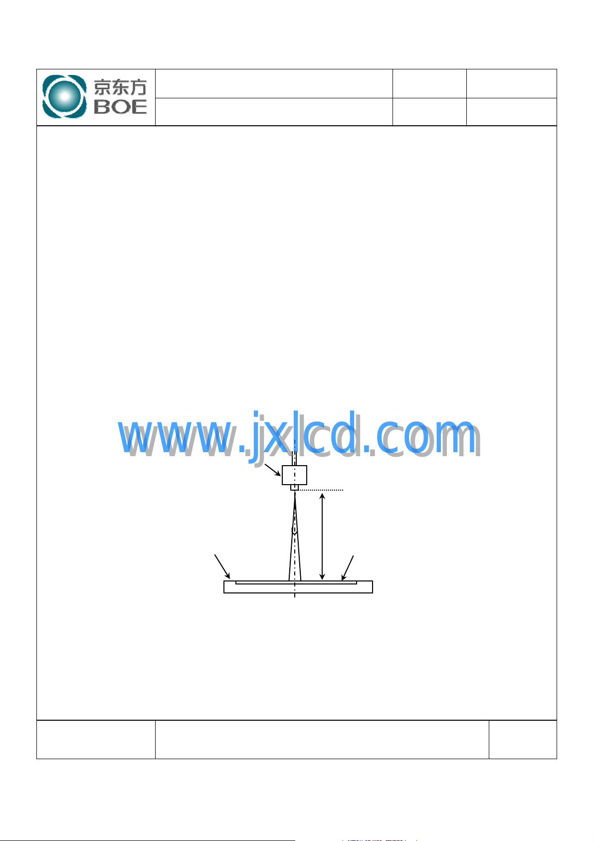
The test of Optical specifications shall be measured in a dark room (ambient luminance ≤ 1
lux and temperature = 25±2℃) with the equipment of Luminance meter system (Goniometer
system and TOPCONE BM-5) and test unit shall be located at an approximate distance
50cm from the LCD surface at a viewing angle of θ and Φ equal to 0°. We refer to θØ=0
(=θ3 ) as the 3 o’clock direction (the “right”), θØ=90 (= θ12 ) as the 12 o’clock direction
(“upward”), θØ=180 (= θ9 ) as the 9 o’clock direction (“left”) and θØ=270(= θ6 ) as the 6
o’clock direction (“bottom”). While scanning θand/or Ø, the center of the measuring spot on
the Display surface shall stay fixed. The backlight should be operating for 30 minutes prior to
measurement... VDD shall be 3.3+/- 0.3V at 25°C. Optimum viewing angle direction is 6
’clock.
4.2 Optical Specifications
<Table 4. Optical Specifications>
RemarkUnitMax.Typ.Min.ConditionSymbolParameter
Deg.-85Deg.-85Deg.-85Deg.-85-
cd/m
%
ms
%2.0--
Note 1
Note 2-500:1-
2
Note 3
Viewing Angle
range
Center
Luminance of
White
White
Luminance
uniformity
White Chromaticity
Reproduction
of color
www.jxlcd.com
www.jxlcd.com
Horizontal
Vertical
1 Point
Red
Green
Blue
Rise Response
DecayTime
Θ
CRLuminance Contrast ratio
CTCross Talk
Θ
Θ
Θ
Y
R
T
3
9
12
6
w
IBL = 6.5mA
x
y
x
y
x
y
x
y
r
d
CR > 10
Θ = 0°
Θ = 0°
Θ = 0°
Ta= 25° C
Θ = 0°
Θ = 0°
30
-200170
-8580ΔY55 Points
-6560ΔY1313 points
0.3410.3130.285W
0.3490.3290.309W
0.6040.5740.544
0.3660.3360.306R
0.3280.2980.268G
0.5830.5530.523G
0.1790.1490.119B
0.1690.1390.109B
-30-
--T
SPEC. NUMBER
S864-1236 9
B2005-C001-O(3/3) A4(210 X 297)
SPEC TITLE
HV150UX1-100 Product Specification for Lenovo
PAGE
OF 30
Page 10
PRODUCT GROUP
Notes : 1. Viewing angle is the angle at which the contrast ratio is greater than 10. The
viewing angles are determined for the horizontal or 3, 9 o’clock direction and the
vertical or 6, 12 o’clock direction with respect to the optical axis which is normal
to the LCD surface (see FIGURE1 as below).
2. Contrast measurements shall be made at viewing angle of Θ= 0 and at the center
of the LCD surface. Luminance shall be measured with all pixels in the view field
set first to white, then to the dark (black) state .
Luminance Contrast Ratio (CR) is defined mathematically as CR = Luminance when
displaying a white raster / Luminance when displaying a black raster.
3. The color chromaticity coordinates specified in Table 4. shall be calculated from
the spectral data measured with all pixels first in red, green, blue, and white.
Measurements shall be made at the center of the panel.
ISSUE DATEREV
2005.12.20ATFT LCD PRODUCT
4.3 Optical measurements
www.jxlcd.com
www.jxlcd.com
Photo detector
( TOPCON BM-5A)
TFT-LCD module
Figure 1. Measurement Set Up
o
Field = 2
Center of the screen
Optical characteristics measurement setup
50 cm
LCD panel
SPEC. NUMBER
S864-1236 10
B2005-C001-O(3/3) A4(210 X 297)
SPEC TITLE
HV150UX1-100 Product Specification for Lenovo
PAGE
OF 30
Page 11
PRODUCT GROUP
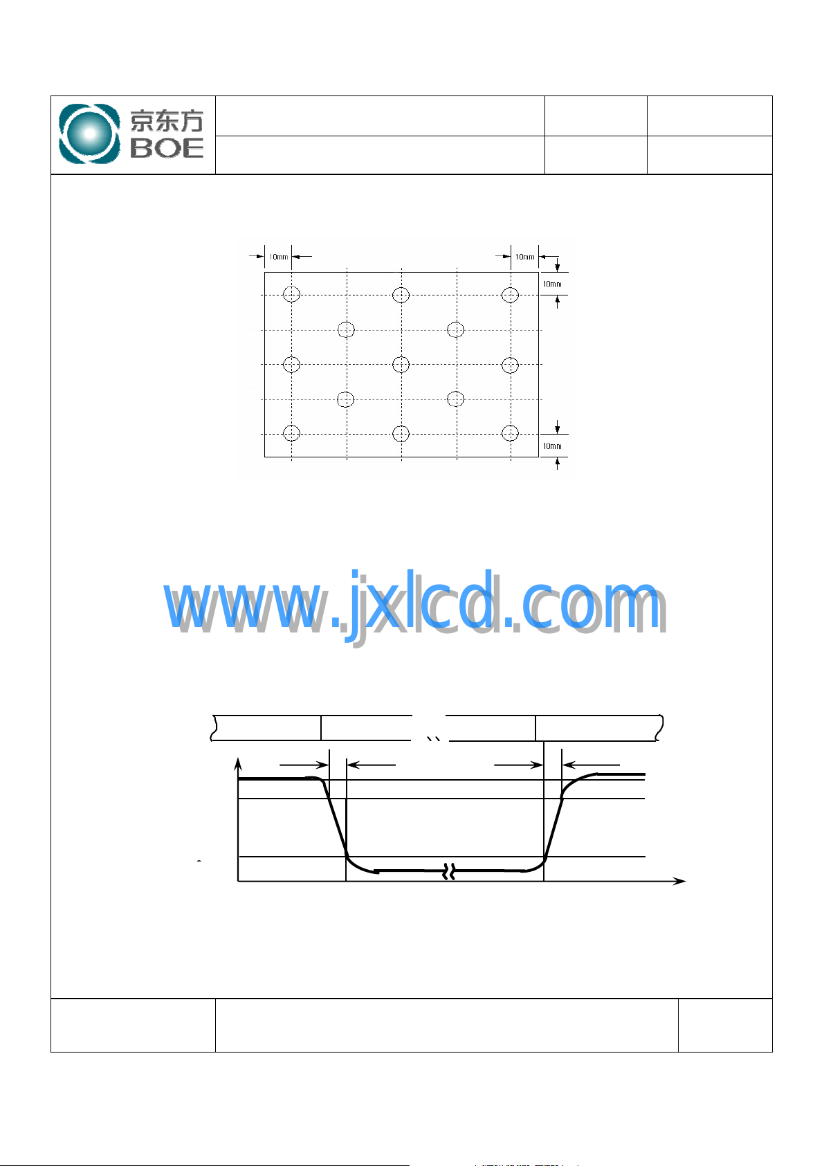
Figure 2. White Luminance (Center) and Uniformity Measurement Locations
(5 and 13points)
400 800 1200
300
600
900
White luminance : Center Luminance of white is defined as luminance values of
center 1 point. Luminance shall be measured with all pixels in the view field set first
to white. This measurement shall be taken at the locations shown in FIGURE 2.
ISSUE DATEREV
2005.12.20ATFT LCD PRODUCT
Uniformity of 5 points and 13 points : The White luminance uniformity on LCD
surface is expressed as : ΔY5 = Minimum Luminance of five points / Maximum
Luminance of five points (see FIGURE 2) , ΔY13 = Minimum Luminance of 13
points /Maximum Luminance of 13 points (see FIGURE 2.)
Display data
Optical
Response
The electro-optical response time measurements shall be made as shown in
FIGURE 3 by switching the “data” input signal ON and OFF. The times needed
for the luminance to change from 10% to 90% is Td and 90% to 10% is Tr.
www.jxlcd.com
www.jxlcd.com
Figure 3. Response Time Testing
White(TFT OFF)
100%
90%
10%
0%
Black(TFT ON)
TR
White(TFT OFF)
TF
Time
SPEC. NUMBER
S864-1236 11
B2005-C001-O(3/3) A4(210 X 297)
SPEC TITLE
HV150UX1-100 Product Specification for Lenovo
PAGE
OF 30
Page 12

PRODUCT GROUP
Figure 4. Cross Modulation Test Description
ISSUE DATEREV
2005.12.20ATFT LCD PRODUCT
VIEW AREA VIEW AREA
Test point of YA/ YB: Horizontal - 1400, 600
Cross-Talk (%) =
Where:
www.jxlcd.com
YA= Initial luminance of measured area (cd/m2)
www.jxlcd.com
YB= Subsequent luminance of measured area (cd/m2)
The location measured will be exactly same position in both patterns
Y
A
L31
Vertical - 800, 150
YB-Y
Y
A
B
400,300
× 100
1200,300
1200,900400,900
L0
Y
B
Cross-Talk of one area of the LCD surface by another shall be measured by
comparing the luminance (YA) of a 25mm diameter area, with all display pixels
set to a gray level, to the luminance (Y
area is driven dark (Refer to FIGURE 4).
SPEC. NUMBER
S864-1236 12
B2005-C001-O(3/3) A4(210 X 297)
SPEC TITLE
HV150UX1-100 Product Specification for Lenovo
) of that same area when any adjacent
B
PAGE
OF 30
Page 13

PRODUCT GROUP
ISSUE DATEREV
2005.12.20ATFT LCD PRODUCT
5.0 INTERFACE CONNECTION.
5.1 Electrical Interface Connection
The electronics interface connector is a model FI-XB30S-HFxx manufactured by JAE. The
mating connector part number is FI-S30S or FI-SE30M or FI-S30S manufactured by JAE.
The connector interface pin assignments are listed in Table 5.
<Table 5. Pin Assignments for the Interface Connector>
FunctionsSymbolTerminal
GNDGND1
Power Supply : +3.3V (typical)VDD2
Power Supply : +3.3V (typical)VDD3
No ConnectionNC5
V
EDID
CLK
DATA
GNDVSS10
GNDVSS13
GNDVSS16
GNDVSS19
GNDVSS22
GNDVSS25
GNDVSS28
EDID
EDID
4
6
7
www.jxlcd.com
www.jxlcd.com
V
EDID
CLK
DATA
EDID
EDID
-LVDS differential data input (R0~R5,G0) (Odd pixel)O_RIN0-8
+LVDS differential data input (R0~R5,G0) (Odd pixel)O_RIN0+9
-LVDS differential data input (G1~G5,B0,B1) (Odd pixel)O_RIN1-11
+LVDS differential data input (G1~G5,B0,B1) (Odd pixel)O_RIN1+12
-LVDS differential data input (B2~B5,HS,VS,DE) (Odd pixel)O_RIN2-14
+LVDS differential data input (B2~B5,HS,VS,DE) (Odd pixel)O_RIN2+15
-LVDS differential Clock input (Odd pixel)O_CLKIN-17
+LVDS differential Clock input (Odd pixel)O_CLKIN+18
-LVDS differential data input (R0~R5,G0) (Even pixel)E_RIN0-20
+LVDS differential data input (R0~R5,G0) (Even pixel)E_RIN0+21
-LVDS differential data input (G1~G5,B0,B1) (Even pixel)E_RIN1-23
+LVDS differential data input (G1~G5,B0,B1) (Even pixel)E_RIN1+24
-LVDS differential data input (B2~B5,HS,VS,DE) (Even pixel)E_RIN2-26
+LVDS differential data input (B2~B5,HS,VS,DE) (Even pixel)E_RIN2+27
-LVDS differential Clock input (Even pixel)E_CLKIN-29
+LVDS differential Clock input (Even pixel)E_CLKIN+30
SPEC. NUMBER
S864-1236 13
SPEC TITLE
HV150UX1-100 Product Specification for Lenovo
PAGE
OF 30
B2005-C001-O(3/3) A4(210 X 297)
Page 14
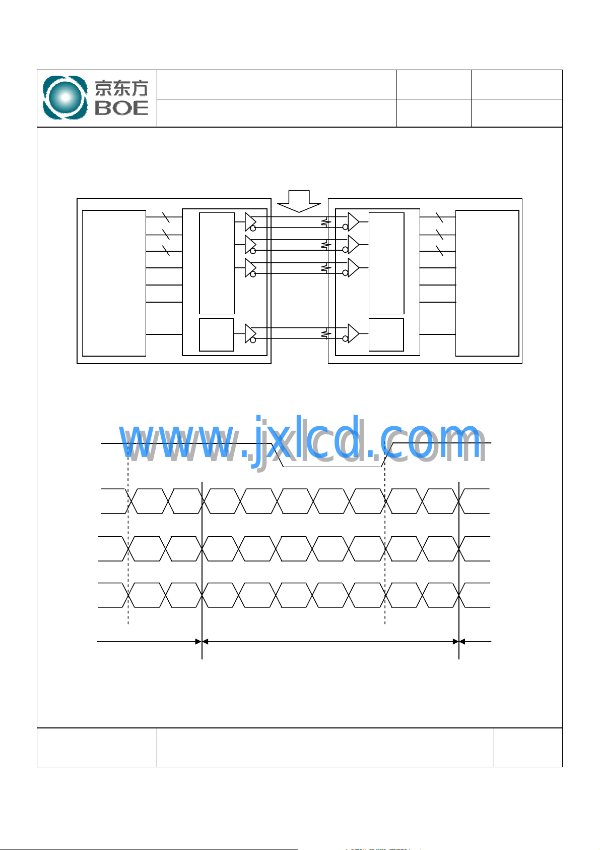
5-2. LVDS Interface
PRODUCT GROUP
ISSUE DATEREV
2005.12.20ATFT LCD PRODUCT
TFT-LCD Side
LVDS to TTL Parallel
PLL
6
6
6
R0~R5
G0~G5
B0~B5
Hsync
Vsync
DE
CLK
R0~R5
G0~G5
B0~B5
Hsync
Vsync
DE
CLK
Notebook PC Side
6
6
6
PLL
CN1
TTL Parallel-to-LVDS
100 ohm
100 ohm
100 ohm
100 ohm
Note. Transmitter : Thine THC63LVDM63A or equivalent. Transmitter is not contained in
Module.
5.3.LVDS Input signal
Vdiff=0V
CLK+
www.jxlcd.com
www.jxlcd.com
Rin0
Rin1
Rin2
G0 R5
B1 B0 G5
Vsync Hsync
DE B5 B4
R4
Signal for 1 DCLK cycle Next cyclePrior cycle
R3 R2 R1
G4
G3
G2
B3
R0
G1
B2
Note. Pin connection in case of using Thine THC63LVDM63A
SPEC. NUMBER
S864-1236 14
SPEC TITLE
HV150UX1-100 Product Specification for Lenovo
PAGE
OF 30
B2005-C001-O(3/3) A4(210 X 297)
Page 15
PRODUCT GROUP
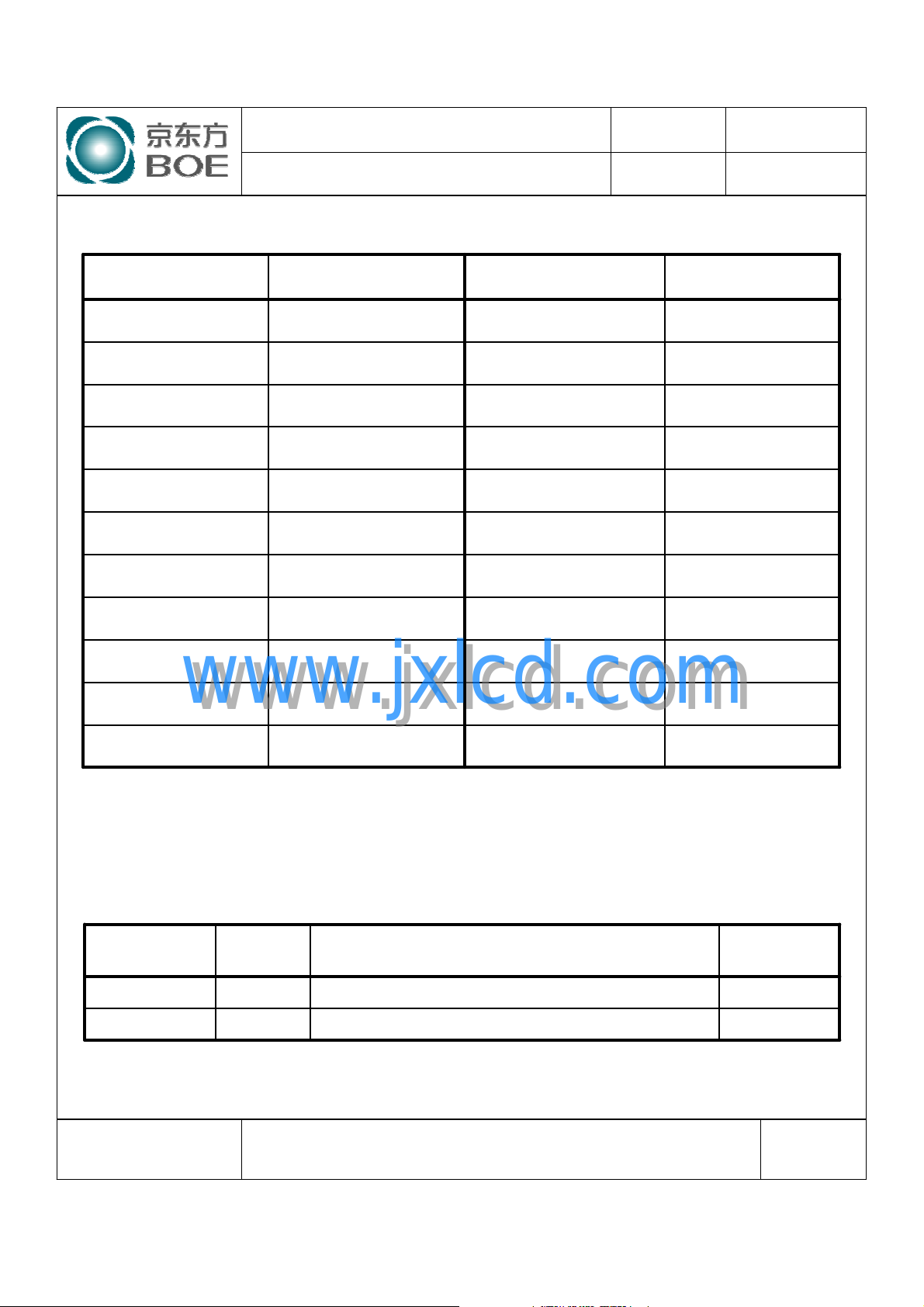
<Table 6. Pin connection in case of using Thine THC63LVDM63A>
ISSUE DATEREV
2005.12.20ATFT LCD PRODUCT
Input signal
www.jxlcd.com
www.jxlcd.com
TransmitterInput signalTransmitter
TB3(10)G4CLK IN(26)DCLK
TB4(12)G5TA0(44)R0
TB5(13)B0TA1(45)R1
TB6(15)B1TA2(47)R2
TC0(16)B2TA3(48)R3
TC1(18)B3TA4(1)R4
TC2(19)B4TA5(3)R5
TC3(20)B5TA6(4)G0
TC4(22)HsyncTB0(6)G1
TC5(23)VsyncTB1(7)G2
TC6(25)DETB2(9)G3
5.4.Back-light Interface
The Back-light interface connector is a model BHSR-02VS-1 manufactured by JST or
equivalent. The connector interface pin assignments are listed in Table 7.
<Table 7. Back-light Electrical Interface>
ColorFunctionSymbolTerminal No.
BlackCCFL Power Supply (GND Side)GL2
SPEC. NUMBER
S864-1236 15
SPEC TITLE
HV150UX1-100 Product Specification for Lenovo
PinkCCFL Power Supply (High Voltage)VL1
PAGE
OF 30
B2005-C001-O(3/3) A4(210 X 297)
Page 16

PRODUCT GROUP
6.0. SIGNAL TIMING SPECIFICATION
The specification of the signal timing parameters are listed in Table 8.
<Table 8. Signal Timing Specification.>
ISSUE DATEREV
2005.12.20ATFT LCD PRODUCT
UnitMaxTypMinSymbolsItem
ms15.8716.6728.57T1Frame Period
ms-16-T2Vertical Display Period
us-13.3-T3One line Scanning Period
us-9.9-T4Horizontal Display Period
MHz858147.251/T5Clock Frequency
7.0 SIGNAL TIMING WAVEFORMS
7.1 Timing wave forms of interface signal
www.jxlcd.com
www.jxlcd.com
T2
DE
DCLK
T5
DE
DATA
SIGNALS
T1
T3
T4
Valid display data (1600 Clocks)
SPEC. NUMBER
S864-1236 16
B2005-C001-O(3/3) A4(210 X 297)
SPEC TITLE
HV150UX1-100 Product Specification for Lenovo
PAGE
OF 30
Page 17

PRODUCT GROUP
7.2 LVDS Rx Interface Timing Parameter
The specification of the LVDS Rx interface timing parameter is listed in Table 9.
<Table 9. LVDS Rx Interface Timing Specification>
msec10.0--tRPLLPLL Set
nsec21.1612.3511.77tRICPCLKIN Period
nsec+0.40.0-0.4tRIP0Input Data 0
nsectRICP/7+0.4tRICP/7tRICP/7-0.4tRIP1Input Data 1
nsec2 ×tRICP/7+0.42 ×tRICP/72 ×tRICP/7-0.4tRIP2Input Data 2
nsec3 ×tRICP/7+0.43 ×tRICP/73 ×tRICP/7-0.4tRIP3Input Data 3
ISSUE DATEREV
2005.12.20ATFT LCD PRODUCT
RemarkUnitMaxTypMinSymbolItem
www.jxlcd.com
www.jxlcd.com
tRIP6
tRIP5
tRIP4
tRIP3
tRIP2
tRIP1
tRIP0
RxINz +/-
* Z = 0, 1, 2
RxCLKIN+/-
Rx2 Rx1 Rx0 Rx6 Rx5 Rx4 Rx3 Rx2 Rx1 Rx0Rx3
Vdiff=0[v]Vdiff=0[v]
tRICP
nsec4 ×tRICP/7+0.44 ×tRICP/74 ×tRICP/7-0.4tRIP4Input Data 4
nsec5 ×tRICP/7+0.45 ×tRICP/75 ×tRICP/7-0.4tRIP5Input Data 5
nsec6 ×tRICP/7+0.46 ×tRICP/76 ×tRICP/7-0.4tRIP6Input Data 6
SPEC. NUMBER
S864-1236 17
B2005-C001-O(3/3) A4(210 X 297)
SPEC TITLE
HV150UX1-100 Product Specification for Lenovo
PAGE
OF 30
Page 18
PRODUCT GROUP
ISSUE DATEREV
2005.12.20ATFT LCD PRODUCT
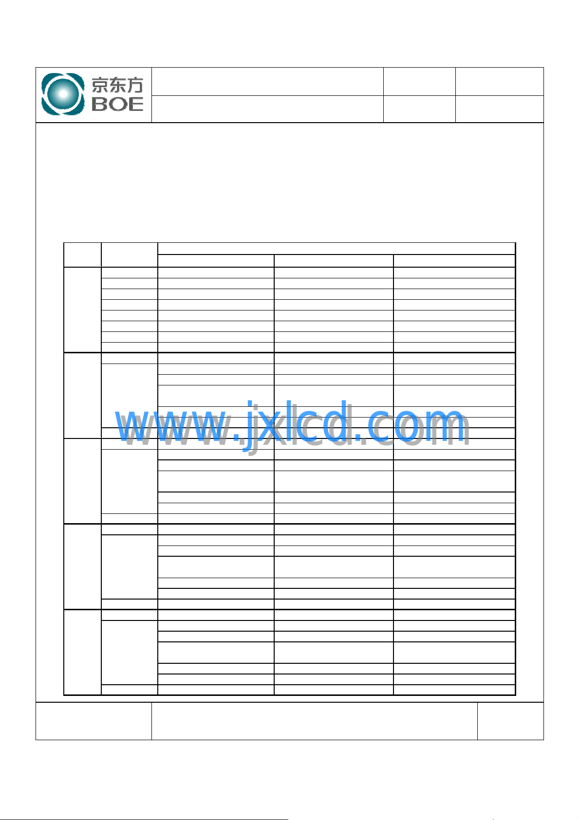
8.0 INPUT SIGNALS, BASIC DISPLAY COLORS & GRAY SCALE OF
COLORS
Each color is displayed in 64 gray scales from a 6 bit data signal input. A total of 262,144
colors are derived from the resultant 18 bit data. Table 10. shows the input signals, basic
display colors and gray scale for each color.
<Table 10. Input signals, Basic display colors and Gray scale for each color.>
Colors & Data signal
Gray scale R0 R1 R2 R3 R4 R5 G0 G1 G2 G3 G4 G5 B0 B1 B2 B3 B4 B5
Black 0 0 0 0 0 0 0 0 0 0 0 0 0 0 0 0 0 0
Blue 0 0 0 0 0 0 0 0 0 0 0 0 1 1 1 1 1 1
Basic Green 0 0 0 0 0 0 1 1 1 1 1 1 0 0 0 0 0 0
colors Light Blue 0 0 0 0 0 0 1 1 1 1 1 1 1 1 1 1 1 1
Red 1 1 1 1 1 1 0 0 0 0 0 0 0 0 0 0 0 0
Purple 1 1 1 1 1 1 0 0 0 0 0 0 1 1 1 1 1 1
Yellow 1 1 1 1 1 1 1 1 1 1 1 1 0 0 0 0 0 0
White 1 1 1 1 1 1 1 1 1 1 1 1 1 1 1 1 1 1
Black 0 0 0 0 0 0 0 0 0 0 0 0 0 0 0 0 0 0
△
Gray Darker 0 1 0 0 0 0 0 0 0 0 0 0 0 0 0 0 0 0
scale
of
Red Brighter 1 0 1 1 1 1 0 0 0 0 0 0 0 0 0 0 0 0
Gray Darker 0 0 0 0 0 0 0 1 0 0 0 0 0 0 0 0 0 0
scale
of
Green Brighter 0 0 0 0 0 0 1 0 1 1 1 1 0 0 0 0 0 0
Gray Darker 0 0 0 0 0 0 0 0 0 0 0 0 0 1 0 0 0 0
scale
of
Blue Brighter 0 0 0 0 0 0 0 0 0 0 0 0 1 0 1 1 1 1
Gra y
scale Darker 0 1 0 0 0 0 0 1 0 0 0 0 0 1 0 0 0 0
of
White
& Brighter 1 0 1 1 1 1 1 0 1 1 1 1 1 0 1 1 1 1
Black
△
▽
▽
Red 1 1 1 1 1 1 0 0 0 0 0 0 0 0 0 0 0 0
www.jxlcd.com
www.jxlcd.com
Black 0 0 0 0 0 0 0 0 0 0 0 0 0 0 0 0 0 0
△
△
▽
▽
Green 0 0 0 0 0 0 1 1 1 1 1 1 0 0 0 0 0 0
Black 0 0 0 0 0 0 0 0 0 0 0 0 0 0 0 0 0 0
△
△
▽
▽
Blue 0 0 0 0 0 0 0 0 0 0 0 0 1 1 1 1 1 1
Black 0 0 0 0 0 0 0 0 0 0 0 0 0 0 0 0 0 0
△
△
▽
▽
White 1 1 1 1 1 1 1 1 1 1 1 1 1 1 1 1 1 1
1 0 0 0 0 0 0 0 0 0 0 0 0 0 0 0 0 0
↓↓ ↓
↓↓ ↓
0 1 1 1 1 1 0 0 0 0 0 0 0 0 0 0 0 0
0 0 0 0 0 0 1 0 0 0 0 0 0 0 0 0 0 0
↓↓ ↓
↓↓ ↓
0 0 0 0 0 0 0 1 1 1 1 1 0 0 0 0 0 0
0 0 0 0 0 0 0 0 0 0 0 0 1 0 0 0 0 0
↓↓ ↓
↓↓ ↓
0 0 0 0 0 0 0 0 0 0 0 0 0 1 1 1 1 1
1 0 0 0 0 0 1 0 0 0 0 0 1 0 0 0 0 0
↓↓ ↓
↓↓ ↓
0 1 1 1 1 1 0 1 1 1 1 1 0 1 1 1 1 1
SPEC. NUMBER
S864-1236 18
SPEC TITLE
HV150UX1-100 Product Specification for Lenovo
PAGE
OF 30
B2005-C001-O(3/3) A4(210 X 297)
Page 19
PRODUCT GROUP
ISSUE DATEREV
2005.12.20ATFT LCD PRODUCT
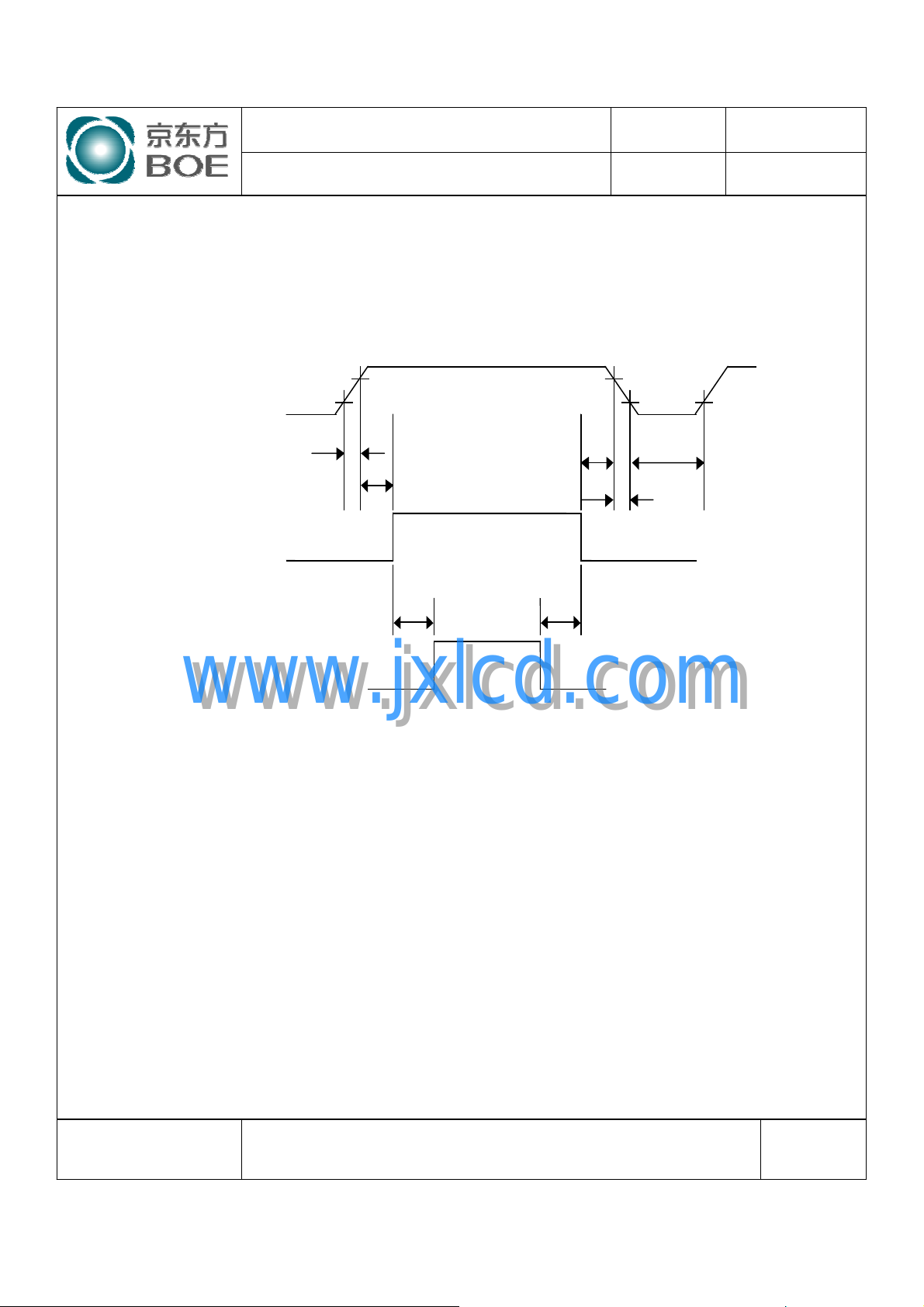
9.0 POWER SEQUENCE
To prevent a latch-up or DC operation of the LCD module, the power on/off sequence shall
be as shown in below
Power Supply
Interface Signal
Back- light
www.jxlcd.com
www.jxlcd.com
0V
0V
0.9VDD
0.1VDD
T1
T2
Valid
T3 T4
0V
● T1 ≤ 10 ms
● 0 ≤ T2 ≤ 50 ms
● 200ms ≤ T3
● 0 ≤ T4
● 0 ≤ T5
● 0 ≤ T6 ≤ 10ms
● 150ms ≤ T7
0.9VDD
T5
0.1VDD
T7
T6
Notes : 1. When the power supply VDD is 0V, Keep the level of input signals on the low or keep
high impedance.
2. Do not keep the interface signal high impedance when power is on.
Back Light must be turn on after power for logic and interface signal are valid.
SPEC. NUMBER
S864-1236 19
B2005-C001-O(3/3) A4(210 X 297)
SPEC TITLE
HV150UX1-100 Product Specification for Lenovo
PAGE
OF 30
Page 20
PRODUCT GROUP
10.0 MECHANICAL CHARACTERISTICS
10.1 Dimensional Requirements
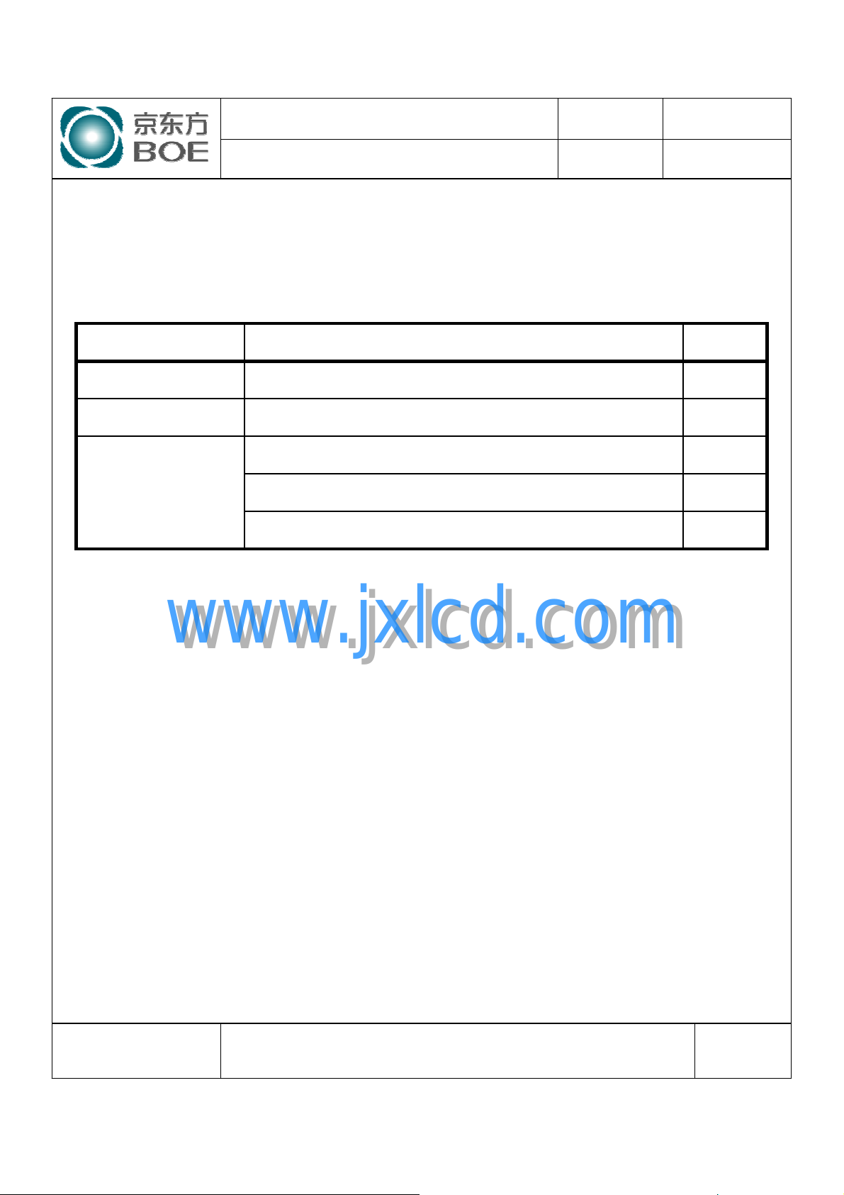
FIGURE 5 (located in Appendix) shows mechanical outlines for the model HV150UX1-100.
Other parameters are shown in Table 11.
<Table 11. Dimensional Parameters>
Connector : BHSR-02VS-1
CCFL, Horizontal & Bottom side lamp typeBack-light
ISSUE DATEREV
2005.12.20ATFT LCD PRODUCT
UnitSpecificationParameter
mm317.3±0.5 ×242.0±0.5×6.5 maxDimensional outline
gram540g (typ.)Weight
mmLength : 40.0±5.0
10.2 Mounting
See FIGURE 5. (shown in Appendix)
www.jxlcd.com
10.3 Anti-Glare and Polarizer Hardness.
The surface of the LCD has an anti-glare coating to minimize reflection and a coating to
reduce scratching.
10.4 Light Leakage
There shall not be visible light from the back-lighting system around the edges of the
screen as seen from a distance 50cm from the screen with an overhead light level of
350lux.
www.jxlcd.com
SPEC. NUMBER
S864-1236 20
B2005-C001-O(3/3) A4(210 X 297)
SPEC TITLE
HV150UX1-100 Product Specification for Lenovo
PAGE
OF 30
Page 21
PRODUCT GROUP
11.0 RELIABLITY TEST
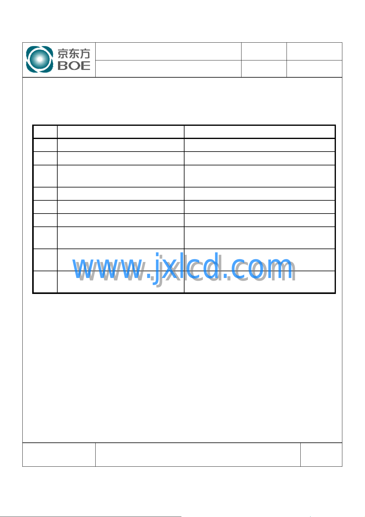
The Reliability test items and its conditions are shown in table 12.
<Table 12. Reliability test>
Ta = 60 ℃, 240 hrsHigh temperature storage test1
Ta = -20 ℃, 240 hrsLow temperature storage test2
ISSUE DATEREV
2005.12.20ATFT LCD PRODUCT
ConditionsTest ItemsNo
3
7
8
9
High temperature & high humidity
operation test
Vibration test
(non-operating)
Shock test
(non-operating)
www.jxlcd.com
www.jxlcd.com
Electro-static discharge test
(non-operating)
Ta = 50 ℃, 80%RH, 1000 hrs
Ta = 50 ℃, 240hrsHigh temperature operation test4
Ta = 0 ℃, 1000hrsLow temperature operation test5
Ta = -20 ℃↔60 ℃ (0.5 hr), 100 cycleThermal shock6
1.5G,10~300Hz for X,Y,Z axis
30 minutes for each axis
220G,2msec,half sine (6 times)
Air : 150 pF, 330Ω, 15 KV
Contact : 150 pF, 330Ω, 8 KV
SPEC. NUMBER
S864-1236 21
B2005-C001-O(3/3) A4(210 X 297)
SPEC TITLE
HV150UX1-100 Product Specification for Lenovo
PAGE
OF 30
Page 22
PRODUCT GROUP
12.0 HANDLING & CAUTIONS
(1) Cautions when taking out the module
y Pick the pouch only, when taking out module from a shipping package.
(2) Cautions for handling the module
y As the electrostatic discharges may break the LCD module, handle the LCD module with
care. Peel a protection sheet off from the LCD panel surface as slowly as possible.
y As the LCD panel and back - light element are made from fragile glass material, impulse
and pressure to the LCD module should be avoided.
y As the surface of the polarizer is very soft and easily scratched, use a soft dry cloth
without chemicals for cleaning.
y Do not pull the interface connector in or out while the LCD module is operating.
y Put the module display side down on a flat horizontal plane.
y Handle connectors and cables with care.
(3) Cautions for the operation
y When the module is operating, do not lose CLK, ENAB signals. If any one of these signals
is lost, the LCD panel would be damaged.
y Obey the supply voltage sequence. If wrong sequence is applied, the module would be
damaged.
(4) Cautions for the atmosphere
y Dew drop atmosphere should be avoided.
y Do not store and/or operate the LCD module in a high temperature and/or humidity
atmosphere. Storage in an electro-conductive polymer packing pouch and under relatively
low temperature atmosphere is recommended.
(5) Cautions for the module characteristics
y Do not apply fixed pattern data signal to the LCD module at product aging.
y Applying fixed pattern for a long time may cause image sticking.
(6) Other cautions
y Do not disassemble and/or re-assemble LCD module.
y Do not re-adjust variable resistor or switch etc.
y When returning the module for repair or etc., Please pack the module not to be broken.
We recommend to use the original shipping packages.
www.jxlcd.com
www.jxlcd.com
ISSUE DATEREV
2005.12.20ATFT LCD PRODUCT
SPEC. NUMBER
S864-1236 22
B2005-C001-O(3/3) A4(210 X 297)
SPEC TITLE
HV150UX1-100 Product Specification for Lenovo
PAGE
OF 30
Page 23
PRODUCT GROUP
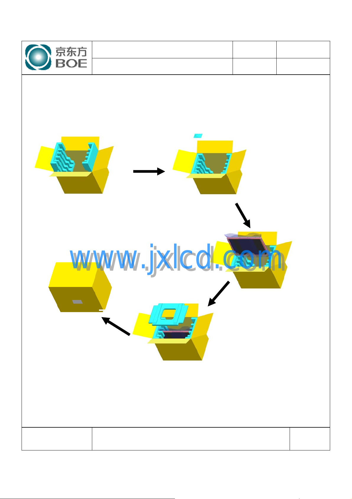
13.0 PACKING INFORMATION
13.1 Packing order
ISSUE DATEREV
2005.12.20ATFT LCD PRODUCT
Put Pad into the
box.
After sealing the
box, attach Packing
Label on the attach
position sign area
of the box.
www.jxlcd.com
www.jxlcd.com
Put silica gels in
the box.
Place a cover on
the top of the box.
As shown in the
figure, place the
Modules bundled by
shielding bag in the
box.
13.2 Notes
zBox Dimension: 333mm(W)X 333mm(D)X 435(H)
zPackage Quantity in one Box: 12pcs
SPEC. NUMBER
S864-1236 23
B2005-C001-O(3/3) A4(210 X 297)
SPEC TITLE
HV150UX1-100 Product Specification for Lenovo
PAGE
OF 30
Page 24

PRODUCT GROUP
14.0 Label
14.1 Packing Label
● Label size : 108 mm (L) X 56 mm (W)
●Contents
Model : HV150UX1-100
Q’ty : Module Q’ty in one box
Serial No. : Box Serial No. See next figure for detail description
Date : Packing Date
FG Code : FG Code of Product
ISSUE DATEREV
2005.12.20ATFT LCD PRODUCT
HV150UX1-100
* 0000000000000 *
www.jxlcd.com
www.jxlcd.com
00 0 00 0 0 000000
Type Grade Year Month ITEM-CODE Serial_no
14.2. High voltage caution label
XXXX
12
20XX.X.XX
1
0
FG CODE
RoHS Mark
SPEC. NUMBER
S864-1236 24
B2005-C001-O(3/3) A4(210 X 297)
SPEC TITLE
HV150UX1-100 Product Specification for Lenovo
PAGE
OF 30
Page 25

14.3. Product Label
14.3.1 BOE HYDIS Barcode
12345 6 7
PRODUCT GROUP
HV150UX1-100
YDTHXXXXXXXXXXXXX
13N7075
13N7076
11S13N7075Z1ZXXXXXXXXX XXX
ISSUE DATEREV
2005.12.20ATFT LCD PRODUCT
X X X X X X X X X X X X X X X X X
Type Designation
No 1. Control number No 5. Month (1, 2, 3, … , 9, X, Y, Z)
No 2. Rank / Grade No 6. Product Identification
No 3. Company (H : BOE HYDIS, O : BOE OT No 7. Serial Number
No 4. Year (4 : 2005, 5 : 2005, … )
14.3.2 Lenovo Barcode
1 1 S 1 3 N 7 0 7 5 Z 1 Z X X X X X X X X X X X X
Type Designation
No 1. Barcode Format ID “ 11S” No 5. Header code
No 2. Part Number No 6. Serial Number No
No 3. Indicator (Should “Z”) No.7. Manufacturing Date Code
No 4. Yamato Control ID “1Z” y : year lower 1 digit
www.jxlcd.com
www.jxlcd.com
1234567
mm : month (01 ~ 12)
SPEC. NUMBER
S864-1236 25
B2005-C001-O(3/3) A4(210 X 297)
SPEC TITLE
HV150UX1-100 Product Specification for Lenovo
PAGE
OF 30
Page 26

PRODUCT GROUP
15.0 EDID data table
EDID chip is 24LC024 (Microchip) or equivalent .
ISSUE DATEREV
2005.12.20ATFT LCD PRODUCT
Add
(Hex)
08
0A
0C
Add
DataField name & comments
Field name & Comments
(Hex)
00Header00
FFHeader01
FFHeader02
FFHeader03
FFHeader04
FFHeader05
FFHeader06
00Header07
ID System Manufacturer Name
: LEN
ID Product Code
: UXGA FFS
www.jxlcd.com
www.jxlcd.com
ID Serial number
30
AE09
46
400B
00
000D
000E
1B
1C
1D
1E
1F
20
21
22
23
24
25
26
27
28
29
Red X : 0.569 (10010001)
Red Y : 0.332 (01010100)
Green X : 0.312 (01001111)
Green Y : 0.544 (100001011)
Blue X : 0.149 (00100110)
Blue Y : 0.132 (00100001)
White X : 0.313 (01010000)
White Y : 0.329 (01010100)
Established timing I
Established Timing II
Manufacturer’s timings
Standard timing ID1 (01h if not used)
Standard timing ID1 (01h if not used)
Standard timing ID2 (01h if not used)
Standard timing ID2 (01h if not used)
Data
91
54
4F
8B
26
21
50
54
21
08
00
81
80
A9
40
000F
00Week of manufacture10
0FYear of Manufacturer : 200511
01EDID Structure version : Ver 1.012
03EDID Revision Number : Rev 313
80Digital I/P, Non TMDS CRGB14
1EMax H image size (cm) : 30.45 cm15
16Max V image size (cm) : 22.8375 cm16
78Display Gamma : 2.217
EAActive off, RGB color18
BDRed/Green low bits = 1011110119
30Blue/White low bits = 001100001A
SPEC. NUMBER
S864-1236 26
SPEC TITLE
HV150UX1-100 Product Specification for Lenovo
2A
2B
2C
2D
2E
2F
30
31
32
33
34
35
Standard timing ID3 (01h if not used)
Standard timing ID3 (01h if not used)
Standard timing ID4 (01h if not used)
Standard timing ID4 (01h if not used)
Standard timing ID5 (01h if not used)
Standard timing ID5 (01h if not used)
Standard timing ID6 (01h if not used)
Standard timing ID6 (01h if not used)
Standard timing ID7 (01h if not used)
Standard timing ID7 (01h if not used)
Standard timing ID8 (01h if not used)
Standard timing ID8 (01h if not used)
01
01
01
01
01
01
01
01
01
01
01
01
PAGE
OF 30
B2005-C001-O(3/3) A4(210 X 297)
Page 27

PRODUCT GROUP
ISSUE DATEREV
2005.12.20ATFT LCD PRODUCT
Add
(Hex)
Horizontal Sync pulse width : 192
Hor Sync offset, PW : pulse width
Vertical image size (mm):228.375 mm
Add
DataField name & comments
Field name & Comments
Data
(Hex)
48Detailed timing descriptor #136
3FPixel clock (MHz) / 1000 : 162 MHz37
40Horizontal active : 160038
30Horizontal blanking : 56039
62Horizontal active : blanking3A
B0Vertical active : 12003B
32Vertical blanking : 503C
40Vertical active : blanking3D
40Horizontal Sync offset : 643E
C03F
13Ver sync offset : pulse width = 1 : 340
0041
30Horizontal image size (mm):304.5 mm42
E443
53
54
55
56
57
58
59
5A
5B
5C
5D
5E
5F
60
Hor Sync offset, PW : pulse width
Horizontal image size (mm):304.5 mm
Vertical image size (mm):228.375 mm
Horizontal & Vertical image size : 0
Horizontal border : 0
Vertical border : 0
Flags : 0
Detailed timing descriptor #3
ASCII data string Tag (Supplier Name)
Horizontal active pixel / 8 - 31
Image Aspect Rate (4:3)
00
30
E4
10
00
00
19
00
00
00
0F
00
A9
43
Horizontal & Vertical image size : 0
www.jxlcd.com
www.jxlcd.com
Horizontal border : 0
1044
0045
00Vertical border : 046
19Flags : 047
BCDetailed timing descriptor #248
34Pixel clock (MHz) / 1000 : 135 MHz49
40Horizontal active : 16004A
30Horizontal blanking : 5604B
62Horizontal active : blanking4C
B0Vertical active : 12004D
32Vertical blanking : 504E
40Vertical active : blanking4F
40Horizontal Sync offset : 6450
C0Horizontal Sync pulse width : 19251
13Ver sync offset : pulse width = 1 : 352
61
62
63
64
65
66
67
68
69
6A
6B
6C
6D
6E
6F
Low refresh rate #1 (50 Hz)
Horizontal active pixel / 8 – 31
Image aspect rate (4:3)
Low refresh rate #2 (40 Hz)
Brightness (1/10 nit)
Feature flag (FFS mode)
Reserved 00H
EISA manufacturer code (3CharacterID)
Compressed ASCII
Panel supplier reserved –product code
(Hex, LSB first)
Detailed timing descriptor #4
ASCII data string Tag (Supplier P/N)
32
A9
43
28
14
02
00
09
E5
00
00
00
00
00
FE
SPEC. NUMBER
S864-1236 27
SPEC TITLE
HV150UX1-100 Product Specification for Lenovo
PAGE
OF 30
B2005-C001-O(3/3) A4(210 X 297)
Page 28

PRODUCT GROUP
ISSUE DATEREV
2005.12.20ATFT LCD PRODUCT
Add
(Hex)
DataField name & comments
00ASCII data string Tag (Supplier P/N)70
31173
35574
30075
55U76
58X77
Add
(Hex)
78
7B
7C
7D
7E
7F
Field name & Comments
1
0
0
SP (space)
Extension Flag
Checksum
Data
31
2D-7948H71
3117A56V72
30
30
0A
00
A7
www.jxlcd.com
www.jxlcd.com
SPEC. NUMBER
SPEC TITLE
PAGE
S864-1236 28
B2005-C001-O(3/3) A4(210 X 297)
HV150UX1-100 Product Specification for Lenovo
OF 30
Page 29

PRODUCT GROUP
Figure 5. TFT-LCD Module Outline Dimension (Front View)
ISSUE DATEREV
2005.12.20ATFT LCD PRODUCT
www.jxlcd.com
www.jxlcd.com
SPEC. NUMBER
SPEC TITLE
PAGE
S864-1236 29
B2005-C001-O(3/3) A4(210 X 297)
HV150UX1-100 Product Specification for Lenovo
OF 30
Page 30

PRODUCT GROUP
Figure 6. TFT-LCD Module Outline Dimensions (Rear view)
ISSUE DATEREV
2005.12.20ATFT LCD PRODUCT
www.jxlcd.com
www.jxlcd.com
SPEC. NUMBER
SPEC TITLE
PAGE
S864-1236 30
B2005-C001-O(3/3) A4(210 X 297)
HV150UX1-100 Product Specification for Lenovo
OF 30
 Loading...