


PROPRIETARY NOTE
THIS SPECIFICATION IS THE PROPERTY OF BOE OT AND SHALL NOT BE
REPRODUCED OR COPIED WITHOUT THE WRITTEN PERMISSION OF BOE OT
AND MUST BE RETURNED TO BOE OT UPON ITS REQUEST
TITLE : HT141WXB-100
Product Specification
Rev. A
www.jxlcd.com
www.jxlcd.com
BEIJING BOE OPTOELECTRONICS TECHNOLOGY
SPEC. NUMBER
S864-5039
PRODUCT GROUP
TFT-LCD
REV.
A
ISSUE DATE
2008.11.04.
PAGE
1
OF 31
B2006-5006-O (1/3) A4(210 X 297) A4(210 X 297)

PRODUCT GROUP
REVISION HISTORY
ISSUE DATEREV
2008.11.04.ATFT LCD PRODUCT
PREPARED DATE DESCRIPTION OF CHANGES ECN NO.REV.
W. Kim2008.10.13.Initial Release-0
W. Kim2008.11.03.Changed Lamp Start Voltage Spec.A
www.jxlcd.com
www.jxlcd.com
SPEC. NUMBER
SPEC TITLE
PAGE
S864-5039
B2006-5006-O (2/3) A4(210 X 297)
HT141WXB-100 Product Specification
OF 31
2

PRODUCT GROUP
Contents
ISSUE DATEREV
2008.11.04.ATFT LCD PRODUCT
PageItemsNo.
4General Description1.0
6Absolute Maximum ratings2.0
7Electrical specifications.3.0
9Optical specifications.4.0
14Interface Connection5.0
www.jxlcd.com
www.jxlcd.com
17Signal Timing Specification6.0
17Signal Timing waveforms7.0
19Input Signals, Display Colors & Gray Scale of Colors8.0
20Power Sequence9.0
21Mechanical Characteristics10.0
22Reliability Test11.0
22Handling & Cautions.12.0
23Label13.0
25Packing information14.0
26Mechanical Outline Dimension15.0
28EDID Table16.0
SPEC. NUMBER
S864-5039
B2006-5006-O (3/3) A4(210 X 297)
SPEC TITLE
HT141WXB-100 Product Specification
PAGE
OF 31
3

PRODUCT GROUP
ISSUE DATEREV
2008.11.04.ATFT LCD PRODUCT
1.0 GENERAL DESCRIPTION
1.1 Introduction
HT141WXB-100 is a color active matrix TFT LCD module using amorphous silicon TFT's
(Thin Film Transistors) as an active switching devices. This module has a 14.1 inch
diagonally measured active area with WXGA resolutions (1280 horizontal by 800 vertical
pixel array). Each pixel is divided into RED, GREEN, BLUE dots which are arranged in
vertical Stripe and this module can display 262,144 colors. The TFT-LCD panel used for this
module is a low reflection and higher color type. Therefore, this module is suitable for
Notebook PC. The DC/AC inverter for back-light driving is not built in this model.
Source Driver
LVDS
Input
Connector (CN )
Signal
LVDS Rx
+
T/CON
Gate Driver
TFT LCD Panel
BACK LIGHT (Fluorescent Lamp)
1280 ×800
1
VDD
www.jxlcd.com
www.jxlcd.com
I2C bus
1.2 Features
z SPWG (Standard Panel Working Group) 14.1”W type WXGA(16:10) Form Factor
z Thin and light weight
z 3.3 V power supply
z 1 Channel LVDS Interface
z Single CCFL (Bottom side/Horizontal Direction)
z 262,144 colors
z Data enable signal mode
z Side Mounting Frame
z Green Product (RoHS product)
z On board EDID chip
z Low driving voltage and low power consumption
DC/DC
Gamma
Vcom
EDID/EEPROM
Backlight Unit
CN2
SPEC. NUMBER
S864-5039
B2006-5006-O (3/3) A4(210 X 297)
SPEC TITLE
HT141WXB-100 Product Specification
PAGE
OF 31
4

PRODUCT GROUP
1.3 Application
z Notebook PC (Wide type)
1.4 General Specification
The followings are general specifications at the model HT141WXB-100. (listed in Table 1.)
<Table 1. General Specifications>
mm303.36 (H) ×189.60 (V) (14.1” diagonal)Active area
ISSUE DATEREV
2008.11.04.ATFT LCD PRODUCT
RemarksUnitSpecificationParameter
www.jxlcd.com
www.jxlcd.com
Dimensional outline
Power consumption
RGB Vertical stripePixel arrangement
Normally WhiteDisplay mode
319.5±0.5 (H) ×205.5±0.5 (V) ×5.5 (D:max)
Glare (Clear Black) / Hard coating 3HSurface treatment
: 5.2
total
pixels1280 (H) ×800 (V)Number of pixels
mm0.237 (H) ×0.237 (V)Pixel pitch
colors262,144Display colors
mm
g390 (typ)Weight
Note 1Bottom edge side, 1-CCFL typeBack-light
WPD: 1.1
WPBL: 4.1
WP
Notes : 1. CCFL (Cold Cathode Fluorescent Lamp)
SPEC. NUMBER
S864-5039
B2006-5006-O (3/3) A4(210 X 297)
SPEC TITLE
HT141WXB-100 Product Specification
PAGE
OF 31
5
PRODUCT GROUP
Temp
(
)
(40,
)
(
)
(
)
ty
ISSUE DATEREV
2.0 ABSOLUTE MAXIMUM RATINGS
The followings are maximum values which, if exceed, may cause faulty operation or
damage to the unit. The operational and non-operational maximum voltage and current
values are listed in Table 2.
Ta=25+/-2°C< Table 2. Absolute Maximum Ratings>
RemarksUnitMax.Min.SymbolParameter
2008.11.04.ATFT LCD PRODUCT
Power Supply Voltage
Logic Supply Voltage
Lamp Current
Lamp frequency
Operating Temperature
Storage Temperature
DD
IN
L
L
OP
SP
+500T
+70-20T
V4.0-0.3V
VVDD+0.3-0.3V
mArms7.02.0I
Note 1
kHz8040F
℃
Note 2
℃
Notes : 1. Permanent damage to the device may occur if maximum values are exceeded
functional operation should be restricted to the condition described under normal
operating conditions.
www.jxlcd.com
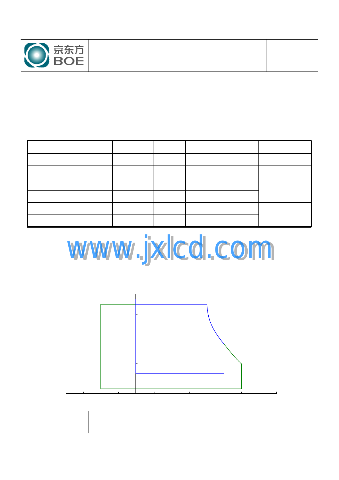
2. Temperature and relative humidity range are shown in the figure below.
www.jxlcd.com
95 % RH Max. ( 40 OC ≥ Ta)
Maximum wet - bulb temperature at 39 OC or less. (Ta > 40 OC) No condensation.
Relative Humudi
100
90
80
90
60
Operating Range
40
20
50, 50
60, 27
Storage Range
5
-40 -20 0 20 40 60 80
SPEC. NUMBER
S864-5039
SPEC TITLE
HT141WXB-100 Product Specification
erature
℃
PAGE
OF 31
6
B2006-5006-O (3/3) A4(210 X 297)

PRODUCT GROUP
3.0 ELECTRICAL SPECIFICATIONS
3.1 Electrical Specifications
ISSUE DATEREV
2008.11.04.ATFT LCD PRODUCT
Power Supply Voltage
Permissible Input Ripple
Voltage
Power Supply Current
High Level Differential Input
Signal Voltage
Low Level Differential Input
Signal Voltage
Back-light Lamp Voltage
www.jxlcd.com
www.jxlcd.com
Back-light Lamp Current
Back-light Lamp operating
Frequency
< Table 3. Electrical specifications >
DD
RF
DD
IH
IL
BL
BL
L
-670-V
IBL= 6.0mA
RemarksUnitMax.Typ.Min.Parameter
Note 1V3.63.33.0V
At VDD= 3.3VmV100--V
Note 1mA400330-I
mV100--V
mV100--V
rms
mA7.06.02.0I
KHz806040F
Note 2V
One Lamp
Note 3
Vrms1,340--
Lamp Start Voltage
Power Consumption
SPEC. NUMBER
S864-5039
B2006-5006-O (3/3) A4(210 X 297)
SPEC TITLE
HT141WXB-100 Product Specification
Vs
BL
total
Vrms1,680--
D
W5.65.2-P
At Ta = 25℃
Note 4
At Ta = 0℃
Note 4
Note 5Hrs-1500010000Lamp Life
Note 1W1.31.1-P
Note 6W4.34.1-P
PAGE
OF 31
7
PRODUCT GROUP
Notes : 1. The supply voltage is measured and specified at the interface connector of LCM.
The current draw and power consumption specified is for 3.3V at 25℃.
a) Typ : Window XP pattern
b) Max : Vertical 2 line skip pattern
2. Reference value, which is measured with Samsung Electric SIC-180 Inverter.
BL Min is value at IBL Min and VBL Max is value at IBL Max)
(V
3. The lamp frequency should be selected as different as possible from the horizontal
synchronous frequency and its harmonics to avoid interference which may
cause line flow on the display.
4. The voltage that must be larger than Vs should be applied to the lamp for more
than 1 second after startup. Otherwise the lamp may not be turned on.
ISSUE DATEREV
2008.11.04.ATFT LCD PRODUCT
5. End of Life shall be determined by the time when any of the following is satisfied
under continuous lighting at 25℃ and I
y Intensity drops to 50% of the Initial Value.
6. Calculated value for reference (VBL × IBL)
www.jxlcd.com
www.jxlcd.com
4.0 OPTICAL SPECIFICATION
4.1 Overview
The test of Optical specifications shall be measured in a dark room (ambient luminance ≤ 1
lux and temperature = 25±2℃) with the equipment of Luminance meter system (Goniometer
system and TOPCONE BM-5) and test unit shall be located at an approximate distance
50cm from the LCD surface at a viewing angle of θ and Φ equal to 0°. We refer to θØ=0
(=θ3 ) as the 3 o’clock direction (the “right”), θØ=90 (= θ12 ) as the 12 o’clock direction
(“upward”), θØ=180 (= θ9 ) as the 9 o’clock direction (“left”) and
θØ=270(= θ6 ) as the 6 o’clock direction (“bottom”). While scanning θand/or Ø, the center
of the measuring spot on the Display surface shall stay fixed. The backlight should be
operating for 30 minutes prior to measurement... VDD shall be 3.3+/- 0.3V at 25°C.
Optimum viewing angle direction is 6 ’clock.
BL = 6.0[mA] Max Only.
SPEC. NUMBER
S864-5039
B2006-5006-O (3/3) A4(210 X 297)
SPEC TITLE
HT141WXB-100 Product Specification
PAGE
OF 31
8

4.2 Optical Specifications
PRODUCT GROUP
<Table 4. Optical Specifications>
ISSUE DATEREV
2008.11.04.ATFT LCD PRODUCT
RemarkUnitMax.Typ.Min.ConditionSymbolParameter
Viewing Angle
range
Luminance of
White
White
Luminance
uniformity
www.jxlcd.com
White Chromaticity
Reproduction
of color
Θ
Θ
3
Θ
9
12
Θ
6
CRLuminance Contrast ratio
Y
w
x
w
w
x
R
R
G
G
CR > 10
Θ = 0°
Θ = 0°
IBL = 6mA
Θ = 0°
Θ = 0°
230200
8580ΔY55 Points
7565ΔY1313 Points
0.3430.3130.283
0.3590.3290.299y
0.6240.5940.564
0.3870.3570.327y
0.5960.5660.536y
Horizontal
Vertical
5 Points
www.jxlcd.com
Red
Green
Deg.-4545
Deg.-4545
Deg.-2515
Deg.-4040
2
Note 1
Note 2500300
Note 3cd/m
Note 4
Note 5
Note 50.3240.2940.264x
0.1790.1490.119x
0.1600.1300.100y
ms16-
Note 610
Note 7%2.0--
PAGE
OF 31
9
Response Time
(Rising + Falling)
SPEC. NUMBER
S864-5039
Blue
B
B
T
RT
CTCross Talk
Ta= 25° C
Θ = 0°
Θ = 0°
SPEC TITLE
HT141WXB-100 Product Specification
B2006-5006-O (3/3) A4(210 X 297)
PRODUCT GROUP
Notes : 1. Viewing angle is the angle at which the contrast ratio is greater than 10. The
viewing angles are determined for the horizontal or 3, 9 o’clock direction and the
vertical or 6, 12 o’clock direction with respect to the optical axis which is normal
to the LCD surface (see FIGURE 1).
2. Contrast measurements shall be made at viewing angle of Θ= 0 and at the center
of the LCD surface. Luminance shall be measured with all pixels in the view field
set first to white, then to the dark (black) state .
(see FIGURE 1) Luminance Contrast Ratio (CR) is defined mathematically.
Luminance when displaying a white raster
CR =
Luminance when displaying a black raster
ISSUE DATEREV
2008.11.04.ATFT LCD PRODUCT
3. Center Luminance of white is defined as luminance values of 5 point average
across the LCD surface. Luminance shall be measured with all pixels in the view
field set first to white. This measurement shall be taken at the locations shown
in FIGURE 2 for a total of the measurements per display.
www.jxlcd.com
4. The White luminance uniformity on LCD surface is then expressed as : ΔY =
5. The color chromaticity coordinates specified in Table 4 shall be calculated from
6. The electro-optical response time measurements shall be made as FIGURE 4
7. Cross-Talk of one area of the LCD surface by another shall be measured by
www.jxlcd.com
Minimum Luminance of 5(or 13) points / Maximum Luminance of 5(or 13) points
(see FIGURE 2 and FIGURE 3).
the spectral data measured with all pixels first in red, green, blue and white.
Measurements shall be made at the center of the panel.
by switching the “data” input signal ON and OFF. The times needed for the
luminance to change from 10% to 90% is Tr, and 90% to 10% is Td.
comparing the luminance (YA) of a 25mm diameter area, with all display pixels
set to a gray level, to the luminance (YB) of that same area when any adjacent
area is driven dark. (See FIGURE 5).
SPEC. NUMBER
S864-5039
B2006-5006-O (3/3) A4(210 X 297)
SPEC TITLE
HT141WXB-100 Product Specification
PAGE
10
OF 31
 Loading...