

Page 1

P
4
T
G
S
P
P
4
4
T
T
G
G
S
S
FCC Statement and Copyright
This equipment has been tested and found to comply with the limits of a
Class B digital device, pursuant to Part 15 of the FCC Rules. These limits
are designed to provide reasonable protection against harmful interference
in a residential installation. This equipment generates, uses and can
radiate radio frequency energy and, if not installed and used in
accordance with the instructions, may cause harmful interference to radio
communications. There is no guarantee that interference will not occur in a
particular installation.
The vendor makes no representations or warranties with respect to the
contents here of and specially disclaims any implied warranties of
merchantability or fitness for any purpose. Further the vendor reserves the
right to revise this publication and to make changes to the contents here of
without obligation to notify any party beforehand.
Duplication of this publication, in part or in whole is not allowed without
first obtaining the vendor’s approval in writing.
The content of this user’s is subject to be changed without notice and we
will not be responsible for any mistakes found in this user’s manual. All the
brand and product names are trademarks of their respective companies.
i
Page 2

C
o
n
t
e
n
t
s
C
o
n
C
o
n
ENGLISH..................................................................................................... 1
P4TGS Features................................................................................................................. 1
Package contents..............................................................................................................1
Layout of P4TGS................................................................................................................2
CPU Installation.................................................................................................................3
SDR DIMM Modules: SDR1-2............................................................................................ 4
Jumpers, Headers, Connectors & Slots.......................................................................... 5
t
e
n
t
s
t
e
n
t
s
ESP AÑOL .................................................................................................10
Características del P4TGS.............................................................................................. 10
Contenido del Paquete.................................................................................................... 10
Disposición del P4TGS ................................................................................................... 11
Instalación de la CPU......................................................................................................12
Módulos SDR DIMM: SDR1-2.......................................................................................... 13
Conectores, Cabezales, Puentes y Ranuras.................................................................14
WARPSPEEDER ................................................................................ ...... 19
Introduction......................................................................................................................19
System Requirement ....................................................................................................... 20
Installation........................................................................................................................20
Usage................................................................................................................................22
TROUBLE SHOOTING.............................................................................30
SOLUCIÓN DE PROBLEMAS .................................................................31
ii
Page 3

M
o
t
h
e
r
b
o
a
r
d
D
e
s
c
r
i
p
t
i
o
n
M
M
o
t
h
e
r
b
o
a
r
d
D
e
s
c
r
o
t
h
e
r
b
o
a
r
d
D
i
e
s
c
r
p
t
i
o
n
i
p
t
i
o
n
English
P4TGS Features
Use Intel 845GL/ ICH4 Chipset, ITE IT8712, LAN Chip- RTL8100B
(optional).
Contains on board I/O facilities, which include one serial port, one VGA port,
a parallel port, a PS/2 mouse port, a PS/2 keyboard port, audio ports, USB
ports, a LAN port (optional) and a game port.
®
Supports the Intel Pentium 4
Supports Ultra 100/66/33, BMIDE and PIO modes.
Supports USB2.0 High Speed Device.
Supports up to 2 SDR 100/133 MHz (without ECC) devices, running at 400
MHz or Fuzzy 533 MHz Front Side Bus frequency.
Supports one CNR Slot (Type A only), and three 32-bit PCI Bus slots.
Complies with PC Micro-ATX form factor specifications.
Supports popular operating systems such as Windows NT, Windows 2000,
Windows ME, Windows XP, LINUX and SCO UNIX.
®
Intel
High S/N ratio meets PC 99 requirements.
6CH DAC, applicable for leading motherboard chipsets.
Line-in phonejack share with rear out.
Mic-in phonejack share with Bass & Center.
Supports front audio pin head functions.
AC’97 2.2 compatible.
(Socket 478) processor up to 3.06GHz.
Package contents
HDD Cable X 1, FDD Cable X 1, Fully Setup Driver CD X 1
Flash Memory Writer for BIOS update X 1
1
Page 4

M
o
t
h
e
r
b
o
a
r
d
D
e
s
M
o
t
h
e
r
b
o
a
r
M
o
t
h
e
USB Cable X 2 (Optional)
Rear I/O Panel for ATX Case X 1 (Optional)
d
r
b
o
a
r
c
D
e
s
d
c
D
e
s
Layout of P4TGS
r
i
p
t
i
o
n
r
i
c
r
p
t
i
o
n
i
p
t
i
o
n
JKBMS1
KB
&
Mouse
USB & LAN
JCOM1
JPRNT1
COM1
Parallel Port
VGA1
JVGA1
Speaker
Out
Game Port
MIC-In Line-In
JGAME_USB1
2
1
JAUDIO1
Codec
JCDIN1
LAN CHIP
JRJ45USB1
ITE I/O
1
JSPDIF_OUT
14
13
1
1
JUSBV1
JATXPWR2
Socket 478
INTEL
845GL
PCI1
JUSBV3
1
PCI2
PCI3
JUSB2
2
1
JUSBV4
10
9
WOL1
11
CNR1
2
1
JUSB1
10
82801DB
9
JCFAN1
1
FDD1
JATXPWR1
SDR1
SDR2
IDE1IDE2
BAT1
INTEL
(ICH4)
2
123
1
JCMOS1
JPANEL1
1
JSFAN1
24
2
Page 5

M
o
t
h
M
o
t
h
M
o
t
h
CPU Installation
e
r
b
o
a
r
d
D
e
s
c
r
i
p
t
i
o
n
e
r
b
o
a
r
d
D
e
s
c
r
e
r
b
o
a
r
d
D
i
e
s
c
r
p
t
i
o
n
i
p
t
i
o
n
1. Pull the lever sideways away from the socket then raise the lever up
to 90-degree angle.
2. Locate Pin A in the socket and lock for the white dot or cut edge in
the CPU. Match Pin A with the white dot/cut edge then insert the
CPU.
3. Press the lever down. Then Put the fan on the CPU and buckle it
and put the fan’s power port into the JCFAN1, then to complete the
installation.
C
P
U
CPU/ System Fan Headers: JCFAN1/ JSFAN1
Ground
12V
Sense
1
JCFAN1
1
Ground
12V
Sense
JSFAN1
3
Page 6

M
o
t
h
e
r
b
o
a
r
d
D
e
s
c
r
i
p
t
i
o
n
M
M
o
t
h
e
r
b
o
a
r
d
D
e
s
c
r
o
t
h
e
r
b
o
a
r
d
D
i
e
s
c
r
p
t
i
o
n
i
p
t
i
o
n
SDR DIMM Modules: SDR1-2
DRAM Access Time: 3.3V Unbuffered PC100/ PC133 Type required.
DRAM Type: 64MB/ 128MB/ 256MB/ 512MB DIMM Module (168 pin)
DIMM Socket
Location
SDR 1 64MB/128MB/256MB/512MB *1
SDR 2 64MB/128MB/256MB/512MB *1
* The list shown above for DRAM configuration is only for reference.
How to install a DIMM Module
1. The DIMM socket has a
“ Plastic Safety Tab”, and the
DIMM memory module has an
“Asymmetrical notch”, so the
DIMM memory module can
only fit into the slot in one
direction.
2. Push the tabs out. Insert the
DIMM memory modules into
the socket at a 90-degree
angle, then push down
vertically so that it will fit into
the place.
3. The Mounting Holes and
plastic tabs should fit over the
edge and hold the DIMM
memory modules in place.
SDR Module Total Memory
Size (MB)
Max is
1GB
4
Page 7

M
o
t
h
e
r
b
o
a
r
d
D
e
s
c
r
i
p
t
i
o
n
M
M
o
t
h
e
r
b
o
a
r
d
D
e
s
c
r
o
t
h
e
r
b
o
a
r
d
D
i
e
s
c
r
p
t
i
o
n
i
p
t
i
o
n
Jumpers, Headers, Connectors & Slots
Hard Disk Connectors: IDE1/ IDE2
The motherboard has a 32-bit Enhanced PCI IDE Controller that
provides PIO Mode 0~4, Bus Master, and Ultra DMA / 33/ 66/ 100
functionality. It has two HDD connectors IDE1 (primary) and IDE2
(secondary).
The IDE connectors can connect a master and a slave drive, so you can
connect up to four hard disk drives. The first hard drive should always be
connected to IDE1.
Floppy Disk Connector: FDD1
The motherboard provides a standard floppy disk connector that
supports 360K, 720K, 1.2M, 1.44M and 2.88M floppy disk types. This
connector supports the provided floppy drive ribbon cables.
Communication Network Riser Slot: CNR1
The CNR specification is an open Industry Standard Architecture, and it
defines a hardware scalable riser card interface, which supports audio,
network and modem only.
Peripheral Component Interconnect Slots: PCI1-3
This motherboard is equipped with 3 standard PCI slots. PCI stands for
Peripheral Component Interconnect, and it is a bus standard for
expansion cards, which has, supplanted the older ISA bus standard in
most ports. This PCI slot is designated as 32 bits.
Power Connectors: JATXPWR1/ JATXPWR2
JATXPWR2
(ATX 12V Power Connector)
JATXPWR1
(ATX Main Power Connector)
5
Page 8

M
o
t
h
e
r
b
o
a
r
d
D
e
s
c
r
i
M
M
o
t
h
e
r
b
o
a
r
d
o
t
h
e
r
b
D
o
a
r
d
D
p
e
s
c
r
i
p
e
s
c
r
i
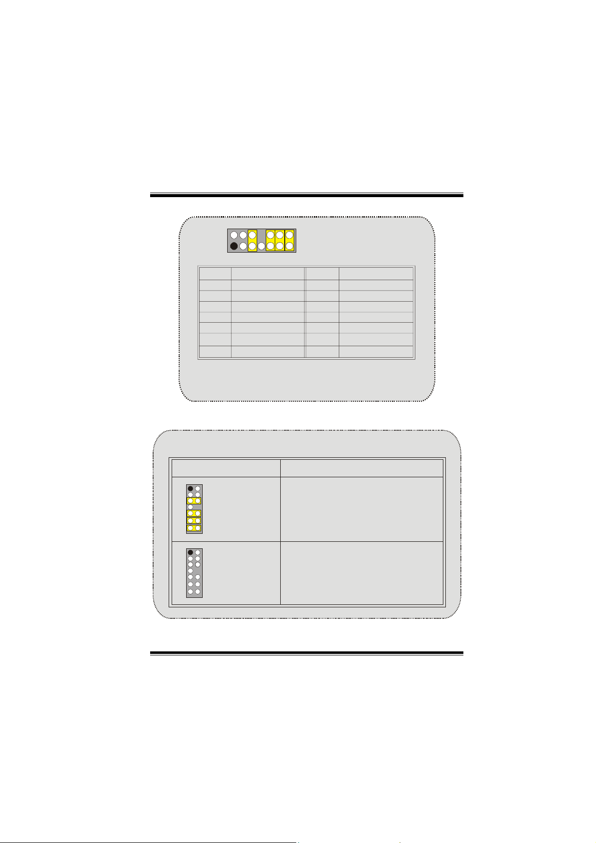
Wake On LAN Header: WOL1
Ground
5V_SB Wake up
1
WOL1
Front USB Header: JUSB1/ JUSB2
t
i
o
n
t
i
o
n
p
t
i
o
n
2
1
JUSB1/2
Pin Assignment Pin Assignm ent
12
+5V +5V
43
Data (-)Data (-)
56
Data (+) Data (+)
Ground Ground
910
Key NA
87
5V/ 5VSB Selection for USB: JUSBV1/ 3/ 4
1
JUSBV1/3/4
Pin 1-2 on ==> 5V
Pin 2-3 on ==> 5V_SB
Digital Audio Connector: JSPDIF_OUT
JSPDIF1
1
Pin Assignment
1
2
3
VCC5
SPDIFO_OUT
GND
6
Page 9

M
M
M
o
t
h
e
r
b
o
a
r
d
D
e
s
c
r
i
p
t
i
o
n
o
t
h
e
r
b
o
a
r
d
D
e
s
c
r
o
t
h
e
r
b
o
a
r
d
D
i
e
s
c
r
p
t
i
o
n
i
p
t
i
o
n
Front Panel Connector: JPANEL1
2
1
PWR_LED
SLP
SPK
(+) (-)(+)
(+) (-)
HLED
RST
SPK ==> Speaker Conn.
HLED ==> Hard Driver LED
RST ==> Reset Button
IR ==> Infrared Conn.
SLP ==> Sleep Button
PWR_LED ==> Power LED
ON/ OFF ==> Power-on Button
Audio Subsystem: JAUDIO1/ JCDIN1
2
1
JAUDIO1
(Front Audio Header)
14
13
JCDIN1
(CD-ROM Audio-In Header)
IRON/OFF
24
23
IR
1
7
Page 10
M
M
M
o
t
h
e
r
b
o
a
r
d
D
e
s
c
r
i
p
t
i
o
n
o
t
h
e
r
b
o
a
r
d
D
e
s
c
r
o
t
h
e
r
b
o
a
r
d
D
i
e
s
c
r
p
t
i
o
n
i
p
t
i
o
n
14
13
JAUDIO1
Pin
2
4
6
8
10
12
14
Assignment
Ground
Audio Power
RT Line Out
Key
LFT Line Out
RT Line In
LFT Li ne In
Pin
1
3
5
7
9
11
13
2
2
1
RT Line Out
LFT Line Out
RT Line In
LFT Line In
Assignment
Mic In
Mic Power
Reserved
Pin 5, 9, 11, 13 are routed to Front Panel Audio Out.
Pin 6, 10, 12, 14 are routed from Front Panel Audio Out.
Front Panel Audio Connector/ Jumper Block
Jumper Setting Configuration
12
4
13
11
3
5
7
9
Pin 5 and 6
6
Pi n 9 a nd 10
Pin11 and 12
10
12
Pin13 and 14
14
Audio line out signals are routed
to the back panel audio line out connector.
12
4
3
6
5
7
9
11
13
10
12
14
No jumpers
installed
Audio line out and mic i n signals are
available for front panel audio connectors.
8
Page 11

M
o
t
h
e
r
b
o
a
r
d
D
e
s
M
M
o
t
h
e
r
b
o
a
r
o
t
h
e
d
r
b
o
a
r
c
D
e
s
d
D
e
s
Clear CMOS Jumper: JCMOS1
1
JCMOS1
Pin 1-2 on ==> Normal Operation
(default)
Pin 2-3 on ==> Clear CMOS Data
Back Panel Connectors
r
i
p
t
i
o
n
c
r
i
c
r
p
t
i
o
n
i
p
t
i
o
n
JKBMS1
PS/2
Mouse
PS/2
Keyboard
JUSBLAN1
LAN(Optional)
USB
COM1
JCOM1
JPRNT1 JGAME1
Parallel
VGA1
JVGA1
Speaker
Out
Game Po r t
Line In
Mic
In
9
Page 12

M
o
t
h
e
r
b
o
a
r
d
D
e
s
c
r
i
p
t
i
o
n
M
M
o
t
h
e
r
b
o
a
r
d
D
e
s
c
r
o
t
h
e
r
b
o
a
r
d
D
i
e
s
c
r
p
t
i
o
n
i
p
t
i
o
n
Español
Características del P4TGS
Usa Chipset Intel 845GL/ ICH4, ITE IT8712, LAN Chip- RTL8100B
(opcional).
Contiene facilidades I/O integrados en la placa madre en el que incluye un
puerto en serie paralelo, un puerto VGA, un puerto paralelo, un puerto para
el ratón PS/2, un puerto para teclado PS/2, puertos de audio, puertos USB,
puerto LAN (opcional) y un puerto para juegos.
®
Soporta procesador Intel Pentium 4
Soporta Ultra 100/66/33, BMIDE y modo PIO.
Soporta Dispositivo de Alta Velocidad USB2.0.
Soporta hasta 2 SDR 100/133 MHz (no incluye ECC) dispositivos,
corriendo a 400 MHz o Fuzzy 533 MHz frecuencia Front Side Bus.
Soporta una ranura CNR (solamente de tipo A), y tres ranuras PCI Bus de
32-bit.
Compatible con la forma de PC Micro-ATX.
Soporta sistemas operativos populares tales como Windows NT, Windows
2000, Windows ME, Windows XP, LINUX y SCO UNIX.
Intel
High S/N ratio meets PC 99 requirements.
6CH DAC, applicable a los chipsets de la place madre.
Entrada de Linea compartido con el rear out.
Entrada de Mic compartido con Bass & Center.
Soporta funciones del cabezal de contactos del audio frontal.
®
AC’97 2.2 compatible.
(Socket 478) hasta 3.06GHz.
Contenido del Paquete
Cable HDD X 1, Cable FDD X 1, Completo Setup Driver CD X 1
10
Page 13

M
o
t
h
e
r
b
o
a
r
d
D
e
s
c
r
i
p
t
i
o
M
o
t
h
e
r
b
o
a
r
d
D
e
s
M
o
t
h
e
r
b
o
a
r
d
Memoria Flash Writer para actualización del BIOS X 1
Cable USB X 2 (Opcional)
Panel trasero I/O para caja ATX X 1 (Opcional)
c
D
e
s
c
n
r
i
p
t
i
o
n
r
i
p
t
i
o
n
Disposición del P4TGS
JKBMS1
JCOM1
JPRNT1
COM1
Puerto Paralelo
VGA1
JVGA1
Salida del
Altavoz
Entrada
de Linea
Game Port
Entrada
de MIC
JGAME_USB1
2
1
JAUDIO1
Codec
JCDIN1
LAN CHIP
JRJ45USB1
ITE I/O
1
JSPDIF_OUT
14
13
1
1
JUSBV1
JATXPWR2
Socket 478
INTEL
845GL
PCI1
JUSBV3
1
PCI2
PCI3
2
1
JUSB2
JUSBV4
10
9
WOL1
11
CNR1
2
1
JUSB1
10
9
JCFAN1
1
JATXPWR1
SDR1
SDR2
BAT1
INTEL
82801DB
(ICH4)
1
JCMOS1
JPANEL1
2
123
FDD1
IDE1IDE2
1
JSFAN1
24
11
Page 14

M
o
t
h
e
r
b
o
a
r
d
D
e
s
c
r
i
p
t
i
o
n
M
M
o
t
h
e
r
b
o
a
r
d
D
e
s
c
r
o
t
h
e
r
b
o
a
r
d
D
i
e
s
c
r
p
t
i
o
n
i
p
t
i
o
n
Instalación de la CPU
C
P
12V
Sense
U
1
Tierr a
12V
Sense
JSFAN1
1. Tire de la palanca del lado del zócalo, luego levante la palanca
hasta un ángulo de 90 grados.
2. Sitúe el contacto A del zócalo y busque el punto blanco o corte el
borde en la CPU. Empareje el contacto A con el punto blanco/
corte del borde, luego inserte la CPU.
3. Presione la palanca para abajo. Ponga el ventilador en la CPU y
abróchelo. Luego ponga el puerto de corriente del ventilador en el
JCFAN1. Y ya habrá completado su instalación.
CPU/ Cabezales del Sistemas de Ventilación: JCFAN1/
JSFAN1
Tierr a
1
JCFAN1
12
Page 15

M
o
t
h
e
r
b
o
a
r
d
D
e
s
c
r
i
p
t
i
o
n
M
M
o
t
h
e
r
b
o
a
r
d
D
e
s
c
r
o
t
h
e
r
b
o
a
r
d
D
i
e
s
c
r
p
t
i
o
n
i
p
t
i
o
n
Módulos SDR DIMM: SDR1-2
DRAM Tiempo de Acceso: 3.3V Unbuffered PC100/ PC133 Tipo
requerido.
DRAM Tipo: 64MB/ 128MB/ 256MB/ 512MB Módulo DIMM (168
Contactos)
Localización
del Zócalo
DIMM
SDR 1 64MB/128MB/256MB/512MB *1
SDR 2 64MB/128MB/256MB/512MB *1
* La lista de arriba para la configuarción DRAM es solamente para
referencia.
Cómo instalar un módulo DIMM
1. El zócalo DIMM tiene una
lengüeta plástica de
seguridad y el módulo de
memoria DIMM tiene una
muesca asimétrica, así el
módulo de memoria DIMM
puede caber solamente en la
ranura de una sóla dirección.
2. Tire la lengüeta hacia
afuera. Inserte los módulos
de memoria DIMM en el
zócalo a los 90 grados, luego
empuje hacia abajo
verticalmente de modo que
encaje en el lugar.
3. Los agujeros de montaje y
las lengüetas plásticas deben
caber por sobre el borde y sostenga los módulos de memoria DIMM en el
lugar.
Módulo SDR
Total del
Tamaño de
Memoria (MB)
Máxima es
1GB
13
Page 16

M
o
t
h
e
r
b
o
a
r
d
D
e
s
c
r
i
p
t
i
o
n
M
M
o
t
h
e
r
b
o
a
r
d
D
e
s
c
r
o
t
h
e
r
b
o
a
r
d
D
i
e
s
c
r
p
t
i
o
n
i
p
t
i
o
n
Conectores, Cabezales, Puentes y Ranuras
Conectores del Disco Duro: IDE1/ IDE2
La placa madre tiene un controlador de 32-bit PCI IDE que proporciona
Modo PIO 0~4, Bus Master, y funcionalida Ultra DMA / 33/ 66/ 100.
Tiene dos conectores HDD IDE1 (primario) y IDE2 (secundario).
El conector IDE puede conectar a un master y un drive esclavo, así
puede conectar hasta cuatro discos rígidos. El primer disco duro debe
estar siempre conectado al IDE1.
Conector para el Disquete: FDD1
La placa madre proporciona un conector estándar del disquete (FDC)
que soporta 360K, 720K, 1.2M, 1.44M y 2.88M tipos de disquete. Éste
conector utiliza los cables de cinta proporcionados por el disquete.
Ranura de Canalización de la Red de Comunicación:
CNR1
La especificación CNR es una abierta Industria Estándar de Arquitectura,
y define una tarjeta hardware escalable de interface en el que soporta
audio, red y módem.
Ranura de Interconexión del Componente Periférico:
PCI1-3
Ésta placa madre está equipado con 3 ranuras PCI. PCI es la sigla para
Interconexión del Componente Periférico, y es un estándar bus para la
tarjeta de expansión en el que reemplaza, en su mayoría de las partes,
al antiguo estándar ISA bus. Las ranuras de PCI están desiñados con
32 bits
Conectores de Encendido: JATXPWR1/ JATXPWR2
(ATX 12V Conector de Corriente)
JATXPWR2
JATXPWR1
(ATX Conector de Corriente Prin cipal)
14
Page 17

M
o
t
h
e
r
b
o
a
r
d
D
e
s
c
r
i
p
t
i
o
n
M
M
o
t
h
e
r
b
o
a
r
d
D
e
s
c
r
o
t
h
e
r
b
o
a
r
d
D
i
e
s
c
r
p
t
i
o
n
i
p
t
i
o
n
Cabezal Wake On LAN: WOL1
Tierr a
5V_SB Wake up
1
WOL1
Cabezal Frontal USB: JUSB1/ JUSB2
Contactos Asignacion Contactos Asignacion
2
1
12
56
910
+5V +5V
Data (+) Data (+)
Ground Ground
Key NA
JUSB1/2
43
87
Data (-)Data (-)
5V/ 5VSB Selección para USB: JUSBV1/ 3/ 4
1
JUSBV1/3/4
Contacto 1-2 on ==> 5V
Contacto 2-3 on ==> 5V_SB
Conector Digital de Audio: JSPDIF_OUT
JSPDIF_OUT
1
Contactos
2
3GND
Asignacion
VCC51
SPDIF_Out
15
Page 18

M
M
M
o
t
h
e
r
b
o
a
r
d
D
e
s
c
r
i
p
t
i
o
n
o
t
h
e
r
b
o
a
r
d
D
e
s
c
r
o
t
h
e
r
b
o
a
r
d
D
i
e
s
c
r
p
t
i
o
n
i
p
t
i
o
n
Conector del Panel Frontal: JPANEL1
2
1
SPK ==> Conector de Altavoz
HLED ==> LED del Disco Duro
RST ==> Boton de Rei n i ci o
IR ==> Conector Infrarojo
SLP ==> Boton de Suspension
PWR_LED ==> Corriente LED
ON/ OFF ==> Boton de Encendido
SLP
SPK
PWR_LED
(+) (-)(+)
(+) (-)
HLED
RST
IRON/OFF
IR
Subsistema de Audio: JAUDIO1/ JCDIN1
2
2
1
1
JAUDIO1
JAUDIO1
(Cabezal de A udio Frontal)
(Front Audio Header)
14
13
JCDIN1
JCDIN1
(CD-ROM Audio-I n Header )
(Cabezal de Entrada de Audio
CD-ROM)
24
23
1
1
16
Page 19

M
M
M
o
t
h
e
r
b
o
a
r
d
D
e
s
c
r
i
p
t
i
o
n
o
t
h
e
r
b
o
a
r
d
D
e
s
c
r
o
t
h
e
r
b
o
a
r
d
D
i
e
s
c
r
p
t
i
o
n
i
p
t
i
o
n
14
13
Contactos
JAUDIO1
2
4
6
8
10
12
14
Corriente de Audio
R T Sal ida de Linea
LFT Salida de Lin ea
RT Entrada de Linea
LFT Entr ada de Line a
Asignacion
Tierra
Key
Contactos
1
3
5
7
9
11
13
2
2
1
Asignacion
Entrada del MIC
Corriente del MIC
RT Salida de Linea
Reservado
LFT Salida de Linea
R T Entrada de L ine a
LFT Entrad a de Lin ea
Contactos 5, 9, 11, 13 son encaminados a la Salida de Audio del
Panel Frontal.
Contactos 6, 10, 12, 14 son encaminados desde la Salida de
Audio del Panel Fron tal.
Conector del Panel Frontal de Audio/ Jumper Block
Jumper Setting Configuracion
12
11
13
4
3
5
7
9
Contacto 5 & 6
6
Contacto 9 & 10
Contacto 11 & 12
10
12
Contacto 13 & 14
14
~
La senal de salida de linea del Audio
encamina al conector de la salida de linea
del Audio ubicado en el panel trasero.
12
4
3
6
5
7
9
11
13
10
12
14
No jumpers
installed
~
La senal de salida de linea del Audio y la
~
senal del entrada del mic estan disponibles
desde el conector de Audio del
panel frontal.
17
Page 20

M
M
M
o
t
h
e
r
b
o
a
r
d
D
e
s
c
r
i
p
t
i
o
n
o
t
h
e
r
b
o
a
r
d
D
e
s
c
r
o
t
h
e
r
b
o
a
r
d
D
i
e
s
c
r
p
t
i
o
n
i
p
t
i
o
n
Puente de Borrar CMOS: JCMOS1
1
Contac to 1 - 2 encendido ==> Operacion Normal (default)
Contacto 2-3 encendido ==> Borrar Datos CMOS
JCMOS1
Conectores del Panel Trasero
Raton
PS/2
RJ45USB1
LAN(Opcional)
USB
JPRNT1
Paralelo
COM1
JCOM1
JKBMS1
Teclado
PS/2
VGA1
JVGA1
JGAME1_USB1
Puerto de Juego
Salida del
Altavoz
Entrada
de Linea
Entrada de
Mic
18
Page 21

M
o
t
h
e
r
b
o
a
r
d
D
e
s
c
r
i
p
t
i
o
n
M
M
o
t
h
e
r
b
o
a
r
d
D
e
s
c
r
o
t
h
e
r
b
o
a
r
d
D
i
e
s
c
r
p
t
i
o
n
i
p
t
i
o
n
WarpSpeeder
Introduction
[ WarpSpeeder™ ], a new powerful control utilit y, features three user-friendly
functions including Overclock Manager, Overvoltage Manager, and Hardware
Monitor.
With the Overclock Manager, users can easily adjust the frequency they prefer
or they can get the best CPU performance with just one click. The Overvoltage
Manager, on the other hand, helps to power up CPU core voltage and Memory
voltage. The cool Hardware Monitor smartly indicates the temperatures, voltage
and CPU fan speed as well as the chipset information. Also, in the About panel,
you can get detail descriptions about BIOS model and chipsets. In addition, the
frequency status of CPU, memory, AGP and PCI along with the CPU speed are
synchronically shown on our main panel.
Moreover, to protect users' computer systems if the setting is not appropriate
when testing and results in system fail or hang, [ WarpSpeeder™ ] technology
assures the system stability by automatically rebooting the computer and then
restart to a speed that is either the original system speed or a suitable one.
19
Page 22

M
o
t
h
e
r
b
o
a
r
d
D
e
s
c
r
i
p
t
i
o
n
M
M
o
t
h
e
r
b
o
a
r
d
D
e
s
c
r
o
t
h
e
r
b
o
a
r
d
D
i
e
s
c
r
p
t
i
o
n
i
p
t
i
o
n
System Requirement
OS Support: Windows 98 SE, Windows Me, Windows 2000, Windows XP
DirectX: DirectX 8.1 or above. (The Windows XP operating system includes
DirectX 8.1. If you use Windows XP, you do not need to install DirectX 8.1.)
Installation
1. Execute the setup execution file, and then the following dialog will
pop up. Please click “Next” button and follow the default procedure
to install.
20
Page 23

M
o
t
h
e
r
b
o
a
r
d
D
e
s
c
r
i
p
t
i
o
n
M
o
t
h
e
r
b
o
a
r
d
D
e
s
c
r
M
o
t
h
e
r
b
o
a
r
d
D
2. When you see the following dialog in setup procedure, it means
setup is completed. If the “Launch the WarpSpeeder Tray Utility”
checkbox is checked, the Tray Icon utility and [ WarpSpeeder™ ]
utility will be automatically and immediately launched after you click
“Finish” button.
i
e
s
c
r
p
t
i
o
n
i
p
t
i
o
n
21
Page 24

M
o
t
h
e
r
b
o
a
r
d
D
e
s
c
r
i
p
t
i
o
n
M
M
o
t
h
e
r
b
o
a
r
d
D
e
s
c
r
o
t
h
e
r
b
o
a
r
d
D
i
e
s
c
r
p
t
i
o
n
i
p
t
i
o
n
Usage
The following figures are just only for reference, the screen printed in this user
manual will change according to your motherboard on hand.
[ WarpSpeeder™ ] includes 1 tray icon and 5 panels:
1. Tray Icon:
Whenever the Tray Icon utility is launched, it will display a little tray ic on on the
right side of Windows Taskbar.
This utility is responsible for conveniently invoking [ WarpSpeeder™ ] Utility.
You can use the mouse by clicking the left button in order to invoke
[ WarpSpeeder™ ] directly from the little tray icon or you can right-click the little
tray icon to pop up a popup menu as following figure. The “Launch Utility” item
in the popup menu has the same function as mouse left-click on tray icon and
“Exit” item will close Tray Icon utility if selected.
22
Page 25

M
o
t
h
e
r
b
o
a
r
d
D
e
s
c
r
i
p
t
i
o
n
M
o
t
h
e
r
b
o
a
r
d
D
e
s
c
r
M
o
t
h
e
r
b
o
a
r
d
D
2. Main Panel
If you click the tray icon, [ WarpSpeeder™ ] utility will be invoked. Please refer
do the following figure; the utility’s first window you will see is Main Panel.
Main Panel contains features as follows:
a. Display t he CPU Speed, CPU external clock, Memory clock, AGP clock,
and PCI clock information.
b. Contains About, Voltage, Overclock, and Hardware Monitor Buttons for
invoking respective panels.
c. With a user-friendly Status Animation, it can represent 3 overclock
percentage stages:
Man walking => overclock percentage from 100% ~ 110 %
Panther running => overclock percentage from 110% ~ 120%
Car racing => overclock percentage from 120% ~ above
i
e
s
c
r
p
t
i
o
n
i
p
t
i
o
n
23
Page 26

M
o
t
h
e
r
b
o
a
r
d
D
e
s
c
r
i
p
t
i
o
n
M
o
t
h
e
r
b
o
a
r
d
D
e
s
c
r
M
o
t
h
e
r
b
o
a
r
d
D
3. Voltage Panel
Click the Voltage button in Main Panel, the button will be highlighted and the
Voltage Panel will slide out to up as the following figure.
In this panel, you can decide to increase CPU core voltage and Memory voltage
or not. The default setting is “No”. If you want to get the best performance of
overclocking, we recommend you click the option “Yes”.
i
e
s
c
r
p
t
i
o
n
i
p
t
i
o
n
24
Page 27

M
o
t
h
e
r
b
o
a
r
d
D
e
s
c
r
i
p
t
i
o
n
M
o
t
h
e
r
b
o
a
r
d
D
e
s
c
r
M
o
t
h
e
r
b
o
a
r
d
D
4. Overclock Panel
Click the Overclock button in Main Panel, the button will be highlighted and the
Overclock Panel will slide out to left as the following figure.
Overclock Panel contains the these features:
a. “–3MHz button”, “-1MHz button”, “+1MHz button”, and “+3MHz button”:
provide user the ability to do real-time overclock adjustment.
Warning: Manually overclock is potentially dangerous, especially
when the overclocking percentage is over 110 %. We strongly
recommend you verify every speed you overclock by click the Verify
button. Or, you can just click Auto overclock button and let
[ WarpSpeeder™ ] automatically gets the best result for you.
b. “Recovery Dialog button”: Pop up the following dialog. Let user select a
restoring way if system need to do a fail-safe reboot.
c. “Auto-overclock button”: User can click this button and [ WarpSpeeder™ ]
will set the best and stable performance and frequency automatically.
[ WarpSpeeder™ ] utility will execute a series of testing until system fail. Then
system will do fail-safe reboot by using Watchdog function. After reboot, the
[ WarpSpeeder™ ] utility will restore to the hardware default setting or load
the verified best and stable frequency according to the Recovery Dialog’s
setting.
i
e
s
c
r
p
t
i
o
n
i
p
t
i
o
n
25
Page 28

M
o
t
h
e
r
b
o
a
r
d
D
e
s
c
r
i
p
t
i
o
n
M
o
t
h
e
r
b
o
a
r
d
D
e
s
c
r
M
o
t
h
e
r
b
o
a
r
d
D
d. “Verify button”: User can click this button and [ WarpSpeeder™ ] will
proceed a testing for current frequency. If the testing is ok, then the
current frequency will be saved into system registry. If the testing fail,
system will do a fail-safe rebooting. After reboot, the [ WarpSpeeder™ ]
utility will restore to the hardware default setting or load the verif ied best
and stable frequency according to the Recovery Dialog’s setting.
Note: Because the testing programs, invoked in Auto-overclock and
Verify, include DirectDraw, Direct3D and DirectShow tests, the
DirectX 8.1 or newer runtime library is required. And please make
sure your display card’s color depth is High color (16 bit) or True
color( 24/32 bit ) that is required for Direct3D rendering.
i
e
s
c
r
p
t
i
o
n
i
p
t
i
o
n
26
Page 29

M
o
t
h
e
r
b
o
a
r
d
D
e
s
c
r
i
p
t
i
o
n
M
o
t
h
e
r
b
o
a
r
d
D
e
s
c
r
M
o
t
h
e
r
b
o
a
r
d
D
5. Hardware Monitor Panel
Click the Hardware Monitor button in Main Panel, the button will be highlighted
and the Hardware Monitor panel will slide out to left as the following figure.
In this panel, you can get the real-time status information of your system. The
information will be refreshed every 1 second.
i
e
s
c
r
p
t
i
o
n
i
p
t
i
o
n
6. About Panel
Click the About button in Main Panel, the button will be highlighted and the
About Panel will slide out to up as the following figure.
In this panel, you can get model name and detail information in hints of all the
chipset that are related to overclocking. You can also get the mainboard’s BIOS
model and the Version number of [ WarpSpeeder™ ] utility.
27
Page 30

M
o
t
h
e
r
b
o
a
r
d
D
e
s
c
r
i
p
t
i
o
n
M
o
t
h
e
r
b
o
a
r
d
D
e
s
c
r
M
o
t
h
e
r
b
o
a
r
d
D
i
e
s
c
r
p
t
i
o
n
i
p
t
i
o
n
28
Page 31

M
o
t
h
e
r
b
o
a
r
d
D
e
s
c
r
i
p
t
i
o
n
M
o
t
h
e
r
b
o
a
r
d
D
e
s
c
r
M
o
t
h
e
r
b
o
a
r
d
D
Note: Because the overclock, overvoltage, and hardware monitor
features are controlled by several separate chipset,
[ WarpSpeeder™ ] divide these features to sep arate panels. If one
chipset is not on board, the correlative button in Main panel will be
disabled, but will not interfere other panels’ functions. This pro perty
can make [ WarpSpeeder™ ] utility more robust.
i
e
s
c
r
p
t
i
o
n
i
p
t
i
o
n
29
Page 32

Trouble Shooting
PROBABLE SOLUTION
No power to the system at all Power light don’t
illuminate, fan inside power supply does not turn
on. Indicator light on keyboard does not turn on
PROBABLE SOLUTION
System inoperative. Keyboard lights are on,
power indicator lights are lit, hard drive is
spinning.
PROBABLE SOLUTION
System does not boot from hard disk drive, can
be booted from CD-ROM drive.
PROBABLE SOLUTION
System only boots from CD-ROM. Hard disk can
be read and applications can be used but
booting from hard disk is impossible.
* Make sure power cable is securely plugged in
* Replace cable
* Contact technical support
* Using even pressure on both ends of the
DIMM, press down firmly until the module
snaps into place.
* Check cable running from disk to disk
controller board. Make sure both ends are
securely plugged in; check the drive type in
the standard CMOS setup.
* Backing up the hard drive is extremely
important. All hard disks are capable of
breaking down at any time.
* Back up data and applications files. Reformat
the hard drive. Re-install applications and
data using backup disks.
PROBABLE SOLUTION
Screen message says “Invalid Configuration” or
“CMOS Failure.”
* Review system’s equipment . Make sure
correct information is in setup.
PROBABLE SOLUTION
Cannot boot system after installing second hard
drive.
* Set master/slave jumpers correctly.
* Run SETUP program and select correct drive
types. Call drive manufacturers for
compatibility with other drives.
30
Page 33

Solución de Problemas
CAUSA PROBABLE SOLUCIÓN
No hay corriente en el sistema. La luz de
corriente no ilumina, ventilador dentro de la
fuente de alimentación apagada. Indicador de
luz del teclado apagado.
CAUSA PROBABLE SOLUCIÓN
Sistema inoperativo. Luz del teclado encendido,
luz de indicador de corriente iluminado, disco
rígido está girando.
CAUSA PROBABLE SOLUCIÓN
Sistema no arranca desde el disco rígido, puede
ser arrancado desde el CD-ROM drive.
CAUSA PROBABLE SOLUCIÓN
Sistema solamente arranca desde el CD-ROM.
Disco rígido puede leer y aplicaciones pueden
ser usados pero el arranque desde el disco
rígido es imposible.
CAUSA PROBABLE SOLUCIÓN
Mensaje de pantalla ”Invalid Configuration” o
“CMOS Failure.”
CAUSA PROBABLE SOLUCIÓN
No puede arrancar después de instalar el
segundo disco rígido.
* Asegúrese que el cable de transmisión esté
* Reemplace el cable.
* Contacte ayuda técnica.
* Presione los dos extremos del DIMM, presione
* Controle el cable de ejecución desde el disco
* Copiando el disco rígido es extremadamente
* Copie datos y documentos de aplicación.
* Revise el equipo del sistema. Asegúrese de
* Fije correctamente el puente master/esclav o.
* Ejecute el programa SETUP y seleccione el
seguramente enchufado.
para abajo firmemente hasta que el módulo
encaje en el lugar.
hasta el disco del controlador. Asegúrese de
que ambos lados estén enchufados con
seguridad; controle el tipo de disco en la
configuración estándar CMOS.
importante. Todos los discos rígidos son
capaces de dañarse en cualquier momento.
Vuelva a formatear el disco rígido. Vuelva a
instalar las aplicaciones y datos usando el
disco de copiado.
que la información configurada sea correcta.
tipo de disco correcto. Llame a una
manufacturación del disco para
compatibilidad con otros discos.
31
Page 34

12/06/2002
32
 Loading...