

ATL Ultramark 9HDI Service Manual

P/N 4730-0013-04 Rev B
£
9
Field Service Manual
Service Manual 4730-0013-04 Rev A consists of:
4720--0013--04 Rev A (2/96)
HDI
August, 1999

A detailed Table of Contents and List of Effective Pages are contained in
Page i. Changed or added pages, from the initial manual release, can be
identified by the change date located at the bottom of each page. No
changedateindicatesthatthispageistheoriginalrelease and has notbeen
changed. A change bar ( ), located in the outside margin of a page,
denotesthespecificpart ofapage thatwaschangedatthatdate.Apointing
hand ( ) indicates the portion of a figure that has been revised.
For a list of current documents, refer to the latest revision of the Active
Documents List -- Ultramark 9 HDI System, P/N 4768-0013-01.

ATL
P.O. Box 3003
Bothell, WA 98041-3003
COPYRIGHTE1996 BY ATL
ALL RIGHTS RESERVED
PRINTEDINUSA
“ATL” , “Advanced Technology Laboratories”, ”Cineloop” , “HDI”, and “Ultramark” are registered trademark of ATL
“Color Power Angio”, “High Definition”, “High Q”, “Power Motion”, and “Tissue Specific” are trademarks of ATL.
Non-ATL product names may be trademarks or registered trademarks of their respective owners.

Introduction
Organization
Introduction
This manual provides only information most often needed in the field.
Experienced personnel will be able to use accompanying performance testing, and preventive maintenance checklists.
The manual contains major tab divisions for diagrams, procedures,
adjustments, fault isolation, configuration supplement, Operating
Notes, Service Bulletins, reference, and parts.
ACTIVE DOCUMENT LIST: lists all active documents pertaining to
the Ultramarkr9 HDI Ultrasound System. Listed are active service
bulletins, service manuals, operation manuals, translated operation
manuals and operating notes.
HDI--i

DIAGRAMS: includes diagrams of system/data paths, power distribution, and cabling.
PROCEDURES: contains information on pre-installation requirements, installation, performance testing, and preventive maintenance.
ADJUSTMENTS: procedures for field authorized adjustments,
including adjustment parameters and location diagrams.
FAULT ISOLATION: system self-diagnostics and fault isolation
information organized by PCB. Also includes minimum configuration
information.
CONFIGURATION: hardware and software compatibility information
for specific system configurations.
OPERATING NOTES: contains operating infor-mation not incorporated into the operation manual.
HDI--ii

SERVICE BULLETINS: includes copies of all active service bulletins. “Hot Tips” may be added as they are received by the CSR.
REPLACEABLE PARTS: contains illustrated parts listings of parts
commonly replaced in the field.
REFERENCE: for information regarding interconnecting cables and
connectors used in the Ultramark 9 HDI as well as other miscellaneous information. This section is currently empty.
Manual Usage and Update Information
The Table of Contents and List of Effective Pages have been combined for this manual. There is no List of Illustrations or List of Tables.
This will facilitate frequent updating of the manual and allow CSRs to
easily determine the effective date of referenced information.
The contents of a manual change package should be inserted as
indicated on the cover sheet attached to the package. Changed or
added pages can be identified by the change date at the bottom of
the affected page. No change date indicates the page is an original
HDI--iii

page. Change bars located in the outside margin of the page denote
the specific part of a page that was changed at that date. A pointing
hand indicates the portion of the figure that has been changed.
Page numbers are divided into three parts. The prefix identifies the
system covered by the manual. The middle portion identifies the section of the manual. The suffix indicates the actual page number.
Safety and Precautions
This section provides biological, procedural, environmental, electrical
and mechanical safety information.
WARNING statements identify conditions or practices that could
result in personal injury or death.
CAUTION statements identify conditions or practices that could result
in equipment damage.
HDI--iv

Biological Safety
The assessment of the biological effects of diagnostic ultrasound on
humans is not complete. Diagnostic ultrasound procedures should be
used only for valid reasons, for the shortest period of time, and at the
lowest power settings necessary to produce diagnostically acceptable images.
Procedural Safety
W ARNING
Do not service or adjust a system unless another
person capable of rendering first aid is present.
CAUTION
Do not sterilize scanheads with heat, liquid, gas, or
solvents. Do not autoclave or expose to temperatures exceeding 50_C(131_F). Permanent damage
may result.
HDI--v

W ARNING
Disconnect power source and scanheads prior to
cleaning.
W ARNING
Inspect the transducer face, housing, and cable
before using the instrument. Do not use damaged
transducers.
W ARNING
Equipment grounding: This equipment is classified
Class I, Type B as defined in IEC Standard 601-1
Safety of Medical Electrical Equipment. Electrical
shock protection is provided by connecting the
instrument chassis to safety ground using the
3-wire power cable provided. This cable must be
connected to a properly grounded receptacle. Do
not defeat the grounding integrity of the equipment.
HDI--vi

W ARNING
Shock hazards exist if the system is not properly
grounded. The system must be plugged into a hospital-grade outlet.
W ARNING
Do not replace components with power connected.
Under certain conditions, dangerous voltages may
exist with power removed. Disconnect power and
discharge circuits before touching.
W ARNING
Fuse replacement is to be done by qualified service
personnel only. Avoid electric shock and fire hazard
by using proper fuses.
CAUTION
Verify the system is set to proper power source
voltage and the cart power plug mates with the
power receptacle.
HDI--vii

W ARNING
Additional hazards may be introduced by using
substituted parts or modified instruments.
W ARNING
Using accessories not recommended by ATL may
cause electrical shock or other unsafe conditions.
CAUTION
Verify circuit boards and components are dry
before applying system power.
CAUTION
This equipment contains components which are
electro-static sensitive. Proper static procedures,
protection and equipment must be used prior to
opening and during handling of this equipment.
Failure to use ESD procedures will cause damage
to these components. Such damage to components
is not covered by ATL warranties.
HDI--viii

Environmental Safety
Do not operate a system in the presence of flammable gases or anesthetics or in an oxygen
enriched environment (i.e., in an explosive atmosphere). An explosion could result.
Mechanical Safety
Use caution when transporting the system over
uneven surfaces, including entry to or exit from elevators.
Stacking equipment on the system, other than ATL
specified equipment, can cause it to become
mechanically unstable.
W ARNING
CAUTION
W ARNING
HDI--ix

Do not use esters or ketone solutions to clean
parts. Discoloration (or worse) will result.
System Safety Symbology
Document IEC601-1, International Electrotechnical Commission:
Safety of Medical Electrical Equipment, classifies patient connections
according to whether the outer enclosure is grounded or floating
(non-conducting). The classifications are shown below.
Grounded chassis. Protection against electrical shock is provided by
connection of chassis to the safety ground (IEC601-1 Type B).
Isolated patient connection (IEC 601-1 Type BF).
Isolated patient connection (IEC 601-1 Type CF).
CAUTION
I and O on circuit breaker and power switch represents ON and OFF,
respectively.
HDI--x

!
IPX--1
This symbol identifies safety note. Be sure you understand the function of this control before using it.
Drip-proof hand-held appliance (transducer assembly). This instrument may be safely handled with wet hands.
Identifies protective earth ground (located next to ground stud on
the rear panel).
Identifies the point where the system safety ground is fastened to the
chassis.
The following a re internal symbols (for reference only):
Identifies high voltage components operating above 1000 VDC or
1500 VAC.
HDI--xi

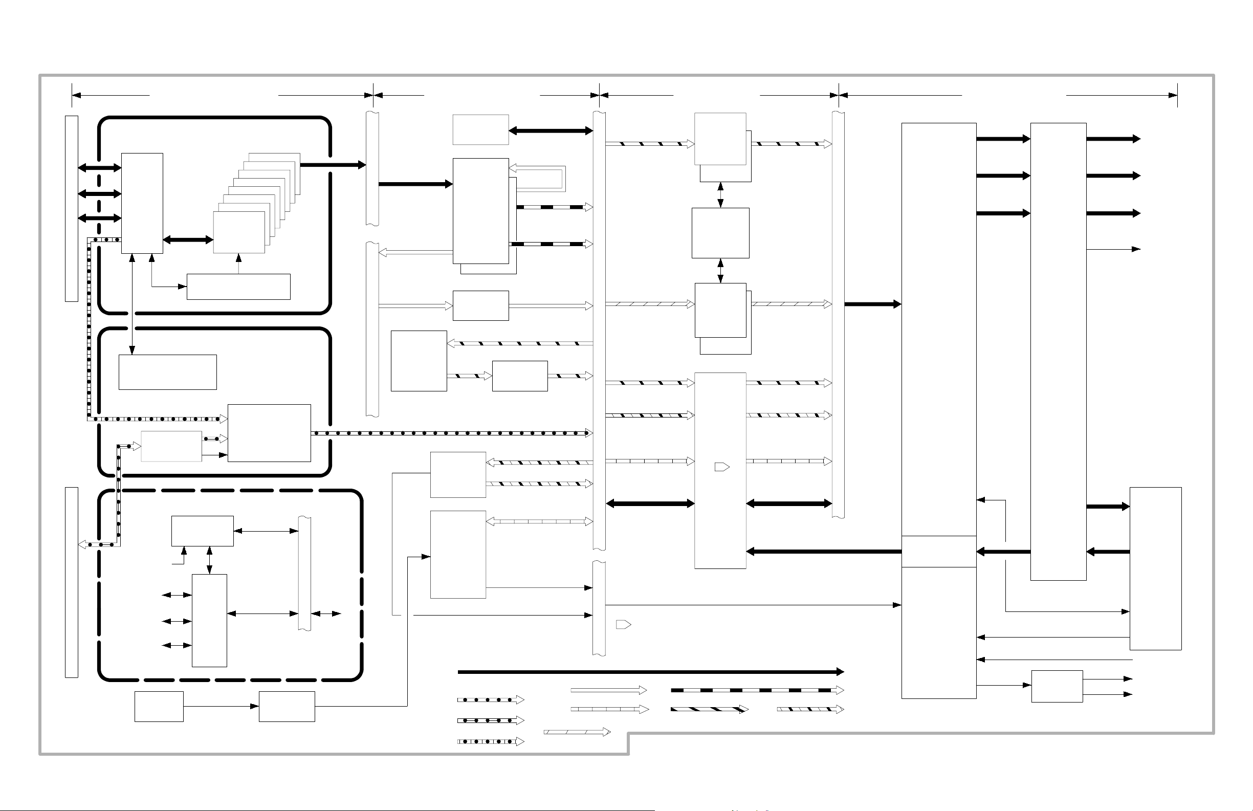
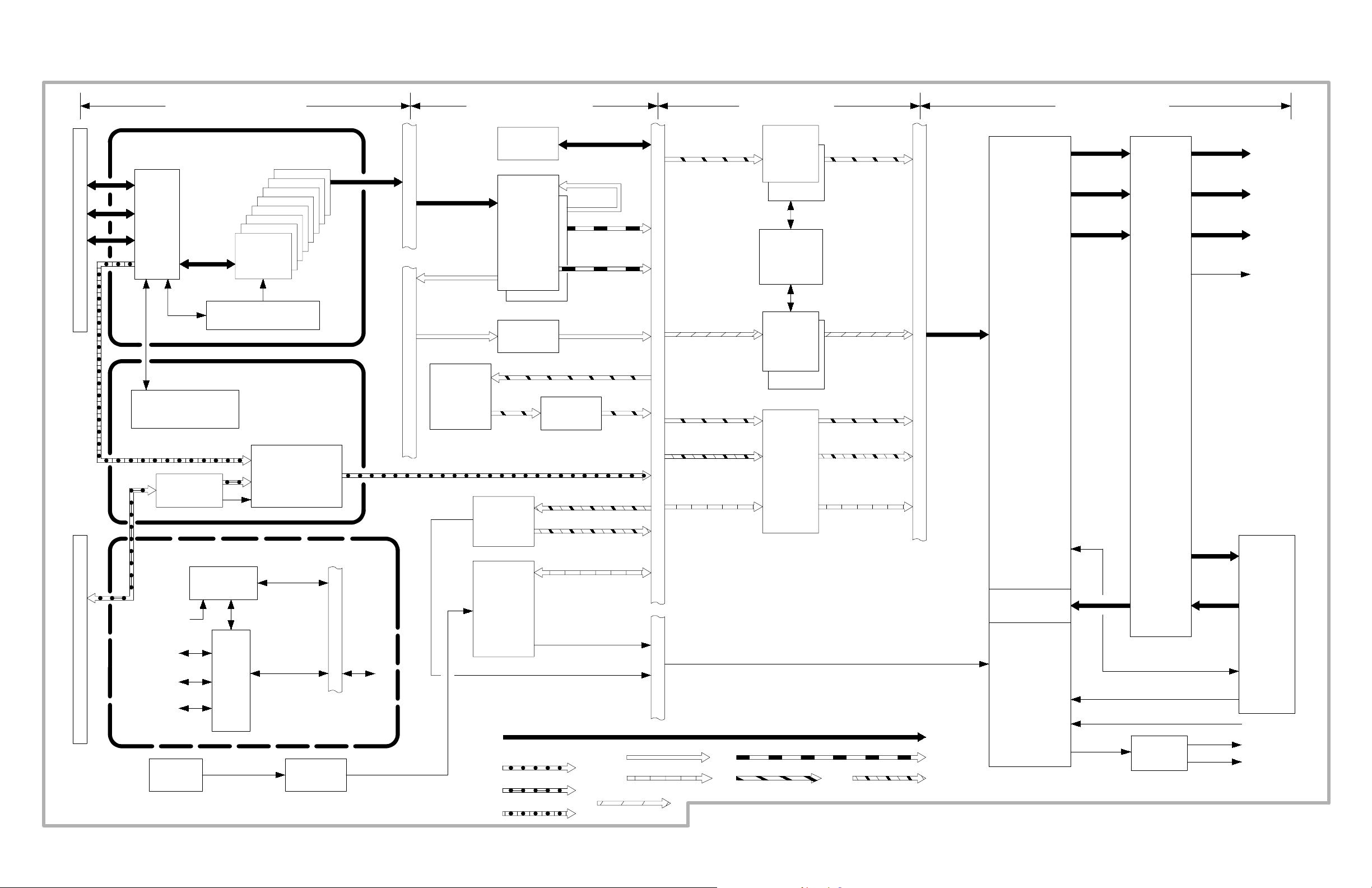
1A Block Diagrams
NOTE:
NOTE:
The block diagrams in this section include PCBs for all
options available for each PCB configuration. Refer to the
following notes as appropriate.
The Doppler Acquisition PCB is installed only if the sys-
D
tem has steered CW or TCD.
The Motor Controller PCB is installed only if the system
D
has A6--3 scanhead capabilities.
Dual IFOM PCBs are installed only on ESP systems. A
D
single IFOM PCB is installed in A16 for Non-ESP systems.
Many PCBs used in Ultramark 9 HDI systems now have
mu ltip le re fere nce designators. Re fer to
PCB slot locations.
Section 5 C
for
HDI-- 1 A--1
)
ACQUISITION GROUP
PROCESSOR GROUP
A
R
R
A
Y
S
C
A
N
H
E
A
D
S
C
W
P
R
O
B
E
S
MECHANICAL
MOTOR CONTROLLER 7500--0617
* Provides WAM motor drive
* Decodes transducer position
* Generates column request to front end
to initiate transmit burst
* SCIP bus interface
* 4 independent power amplifiers with auto--shutdown
if preset power limits are exceeded
2D ACQUISITION, (MFE1) 7500--0655
* Generates 120 MHz system clock
* Part of static CW Doppler transmit andreceive
preamp
* General I/Q reference clock
* Static TCD pulser and preamp
DOPPLER ACQUISITION, (MFE2) 7500--0615
* Required for steered CW, T CD, and static CW
* Receives RF signals from beamformer or MFE1
* Filters and amplifies the RF signal
* Mixes RF down to basebandfrequency
* Low and highpass filtering of baseband frequency
* Audio amplification
* A/D conversion
* Digital control of filtering and amplification
Refer to Tables 5C--1and 5C--2for PCB slot locations.
1
2
Generates 120 MHz clock on ST CW systems
and on Non--steered CW systems with the
7500--0570 FEC. On newer systems without
ST CW/CW, the 2DAcquisition will not be
installed. In this case, the 120 MHz clock
originates from the 7500--0754 FEC.
3
The MFE1 is not in thesteered CW data path.
It generates static CW/TCD transmit pulses
and is in receive data path for static CW/TCD.
For steered CW, the system uses more thanone
element for TX and RX. Steered CW transmit and
receive signals must be routed thru thebeamformer
to provide summation.
1
3
2
ARRAY
FRONT--END CONTROLLER, 7500--0570
* Generates SCIP Bus master clock
for ADDA, IFO, MMC, FEC, and CPU PCB’s
* TGC generation
* Header generation
* High PRF
* PRI sequencing
* Generates transmit and receive delays
* Provides all control and PRI timing functions
for various front ends
* Provides all system backplane clocks
* The 7500--0754 PCB has 120 MHz system clock
when used in non--steered CW only
SCANHEAD SELECT, 7500--0629
* Scanhead interface: linear and phased
Array path via relay to Channel PCB’s
* Scanhead personality interface
* TGC Summation Bus
* CW Summation Bus
* Steered CW path via coax to MFE2
SCANHEAD SELECT DAUGHTER 7500--0636
* Decodes control signals from FEC to Scanhead
Select PCB and pulser power supplies
* Monitors high voltage and +12V on Scanhead
Select PCB
* Interface decoded scanhead personality data from
Scanhead Select PCB back to FEC PCB
* Decodes control data from FEC to HV Mux
ICs in L10--5 scanhead
* Decodes control data from FEC to relays in
Scanhead Select PCB
* S/H temperature monitor
* TGC voltage monitor
CHANNEL, 7500--0544
* 128 transmit pulser elements (16/Channel PCB)
* 128 channel receive apertures
* Echo Summation
* Summed Steered CW toScanhead Select Interface
* TGC waveform generation
* All Channel PCB’s required for scanhead
operation but not required for scanhead ID.
* Applies transmit and receive delays
* Applies TGC to Echo RF data
7500--0755
7500--0772
7500--0754
A
E
C
H
O
B
U
S
B
E
C
H
O
B
U
S
IMAGE BUS MEMORY, 7500--0405
* 256 pages of system memory for 7500--0405 and
7500--0722 PCB’s
* 1024 pages of system memory for 7500--0569PCB
* Stores 2D Cineloop, Doppler,and Doppler
data review
* Manages transfer of Doppler,Color,M--Mode,
and ECG data toImage Bus
* Generates timing signals for memory
* Determines priority of PCB’s requesting
memory time
* Refresh timing
* Image Bus control
IF OUTPUT,7500--0592 (Stand--alone)
* Color samples from RF Data
* Demodulation and bandwidth limiting
* Array sample volume generation
* Doppler Cineloop Limits,Reset, and
Frame Number
* Line density
* Echo detection and compression
* 2D dynamic range
* Self--test capability
* Transfers color and Pulsed Doppler to
Image Memory
* CW Doppler memory addressing
* Participates in 2D depth scaling
* Receives beamformed RF data and performs
demodulation and bandpass filtering to produce
in--phase and quadrature complex data samples
* Creates Image Bus addresses for a color flow
test pattern
IF OUTPUT MASTER/SLAVE, 7500--0783
* Same functions as 7500--0592 IFOM
* Doubles through--put
* Used only on systems with ESP capability
ECHO INPUT MODULE, 7500--0692
* Final 2D and M--Mode depth scaling
* Cineloop memory addressing
* M--Mode enhance
* Receives detected echo data from array front
end, processes data, and writes processed
data to image memory
* Needed for generation oftiming signals sent
through M--Mode/Physio to the Scrolling
Graphics Display
7500--0722
7500--0783 (Stand--alone)
ADVANCED DIGITAL DATA ANALYZER, 7500--0603
* FFT processing
* Array Pulsed Doppler wall filters
* Doppler audio
* Color capture
* Doppler audio synthesis and output
* Doppler signal optimization
* Overall supervision and control of Doppler
processing
* Image memory processing tasks
(edge detection, Doppler history reconstruction,
and color capture)
* Spectral estimation and display processing
* Color Persistence
* ADDA is the only PCB touse Image Bus for
checksum
M--MODE/PHYSIO PROCESSOR, 112--25337
* M--Mode Zoom
* Physio processing: ECG, pulse,
phono displays
* Acquires M--Modedata and performs temporal
averaging to produce visible M--Mode sweep
rates
* Digitizes physiological information from
ECG Isolation PCB, attaches it to processed
M--Mode and sends it to Image Memory
* Generates timing signals for Color M--Mode
and sends them toScrolling Graphics Display
COLOR DATAPROCESSOR, 7500--0602
* Array color wall filter
* Dynamic Motion Differentiation
* Spectral Estimator interface
* Removes Doppler signals coming from stationary
or slow moving structures
* Eliminates high amplitude, low frequency echoes
SPECTRAL ESTIMATOR, 7500--0382
* Generates Color Flow display parameters
* Stores color data in Image Memory
* Estimates frequency, velocity, andstrength
of the returned signal
* Interface with the CDP
* Sends color frame interrupt to system CPU
7500--0671
7500--0829
I
M
A
G
E
B
U
S
A
U
D
I
O
B
U
S
ECG ISOLATION, 3500--1319
* ECG receiver and preamp
* Pulse and phono receiver and preamp
Figure 1A--1. UM--9 HDI PCB Functions (1 of 2
10 ES01--B01 19
HDI-1A-2
)
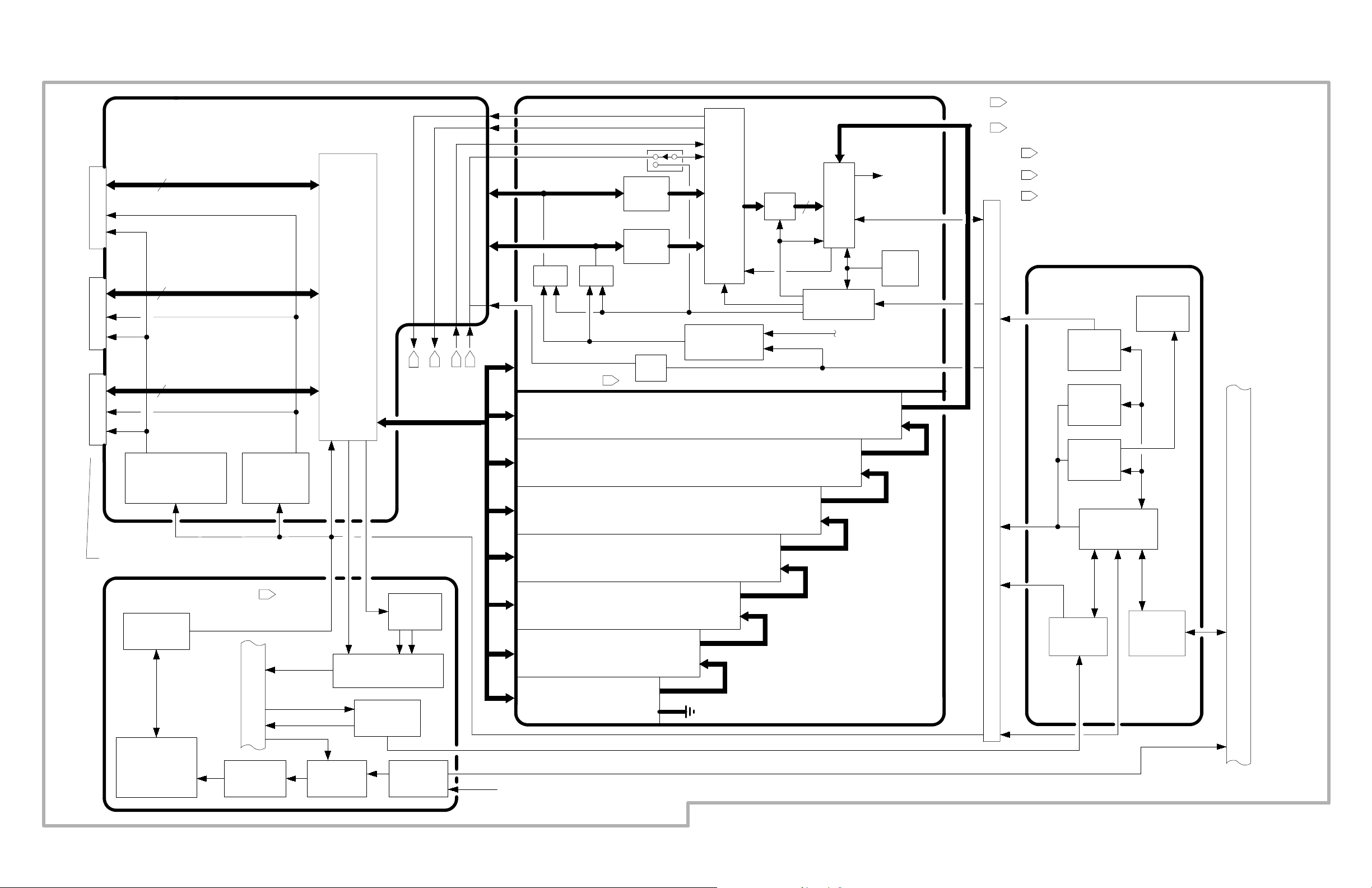
CONTROL GROUP
IMAGE GROUP
DISPLAY GROUP
CONTROL INTERFACE, 7500--0528
* LED Function
* Interface between front panel controls
and system CPU
* I/O port for MIC
* Self test feature
* Soft click audio output
P
H
Y
S
I
O
S
E
N
S
O
R
S
Mode Switch PCB, 7500--0441
Footswitch PCB
* Controls footswitch operation
TactSwitch PCB, 7500--0436
* Front panel pushbuttons, status LED’s,
control panel speaker, rotary controls,
encoder controls
* Switch daughterboard PCB provides
encoder controls (2D, DOPPLER, and
COLORGAINcontrol)
Trackball Switch PCB, 7500--0442
* S1 (Enter), S2 (Set), Trackball
SYSTEM CPU, 7500--0573
* Hard disk control
* Floppy disk control
* System controller (32--bit microprocessor)
* System clock
* Measurement and Analysis
* RS--232 interface
* Monitors critical analog voltages
* Real--time clock and backup
* Stores user defaults
7500--0749
7500--0757
I
M
A
G
E
C
O
N
T
R
O
L
B
U
S
B
U
S
A
U
D
I
O
B
U
S
2D SCAN CONVERTER
*5PCBset
* Formats ultrasound input data into sector or linear rectangular--
coordinate output synchronized to TV raster timing
* Frame averaging (Dynamic Contrast Enhancement)
* 2D pan zoom
* Image orientation (reversal and inversion)
* Interpolates image display data
* Sets display boundaries
S.C. Output Address Generator PCB (B/W and Color) 7500--0499
* Uses CPU timing and control data from the system CPU and the
respective Interface PCB (B/W or Color) to create row and
column display addresses
S.C. Interface PCB (B/W or Color) 7500--0557
* Transfers control messages from the Image Bus to the respective
Output Address Generator PCB and theDual Buffer Memory PCB
* Transfers image data from ImageMemory to the Dual Buffer
* Receives and interpolates display data from the Dual Buffer
Memory PCB and transfers it tothe Video Bus
* Performs frame averaging function (Dynamic Contrast Enhancement)
Dual Buffer Memory PCB 7500--0558
* Provides image data storage for the 2Dscan converter module
* Modifies the display address from the OutputAddress Generator
PCB, and uses thataddress to select the correct data from
the memory array for transfer to theInterface PCB
DISPLAY GRAPHICS, 7500--0514 COLOR
* Scrolling spectral display
* Color M--Mode display
* Doppler ECG display
ADVANCED VIDEO PROCESSOR, 3500--1200 (NTSC)
* All non--scrolling general purpose
graphics
* Grayscale/color mapping
* Generates RGB signals
* Image processing curves
* Doppler grayscale curves
* All system video timing
V
I
D
E
O
B
U
S
* Graybar/Colorbar generator
* VCR remote control and framegrab sync
* Audio preamplification
* Hidden digital overlay for tape directory
* Audio buffer mute control
* Color vs. echo overwrite
REAR PANEL,
3500--1257(NTSC)
3500--1256(PAL)
3500--1511(NTSC/PAL)
* Video switch matrix
* Video sync distribution
* RS--232/422 port
* PAL/NTSC generation
* Video Format Converter PCB, or Video Encoder/
Decoder PCB used as daughter boards
(NTSC or PAL) 7500--0506/0758
* Video output buffer
* Volume control interface (12V)
* Receives 3 different RGB video signals
* Accepts, buffers and distributes
video signals
* Provides DC restored video to theAVP
for frame grabbing
3500--1201 (PAL)
3500--1444 (PAL)
VIDEO
MONITORS
EXTERIOR
VIDEO
MONITOR
HARDCOPY
FRAME
SYNC
VCR
LAMBDA POWER SUPPLY
* Generates +/--48 volts to pulser
PULSER POWER SUPPLY, 3500--1131
* Generates pulser voltage
* Receives +/--48V and converts to transducer pulser voltage
which is variable to +/-- 105V, depending on the scanhead
type, system type, and mode ofoperation
DIGITAL POWER SUPPLY (L.H. RESEARCH)
* Converts 120 VACinto +5 VDC, --5.2 VDC, and +/-- 12 VDC
ANALOG POWER SUPPLY
* Six discrete power supplies which convert 120 VAC
to +6V,--6V, +15V, --15V, +16.5V, --16.5V
1
Frame Grabber functional only on systems
with 17.X software andup.
2
Frame Grabber functions of the Advanced
Frame Grabber PCB functional only on
systems with 17.X software and up.
MASTER SCROLLING GRAPHICS, 7500--0515
* 2D ECG display
* Scrolling M- -Modedisplay
* M--mode ECG display
SCROLLING GRAPHICS DISPLAY, 7500--0864
* Combines all functions of Display Graphics (7500--0514) and Master Scrolling
Graphics (7500--0515)
FRAME GRABBER, 7500--0556
* 4 on 1Save--Recall Format (only on systems without Advanced Frame Grabber)
* VCR Freeze Frame
* Patient Directory
* Hidden Digital
ADVANCED FRAME GRABBER, 7500--0554
* Combines all functions of Display Graphics (7500--0514) and Master Scrolling
Graphics (7500--0515) and Frame Grabber (7500--0556) Refer to PCB functions
listed above for each of thesePCB’s. 2
* Grabs video data and stores in ImageMemory
* Retrieves video data from Image Memory for display
* Scrolling graphics for M--Mode,Doppler, ECG and Physio
* Retrieves Hidden Digital information from VCR playback signal
Refer to PCB functions listed above for each of these PCB’s.
1
AUDIO BUFFER, 7500--0433
* Volume control
* Headphone audio amplifier
* Speaker audio amplifier
* Real time right and left Doppler audio
* VCR playback of right and leftchannel Doppler audio,
and right channel microphone audio
BACKPLANE MOTHERBOARD, 7500--0588
* Signal distribution
* Structural support
* Power distribution
* Ground plane
* Multi--layer PCB
FAN SPEED CONTROLLER, 2100--0679
7500--0677
Figure 1A--1. UM--9 HDI PCB Functions (2 of 2
10 ES01--B02 15
HDI--1A--3
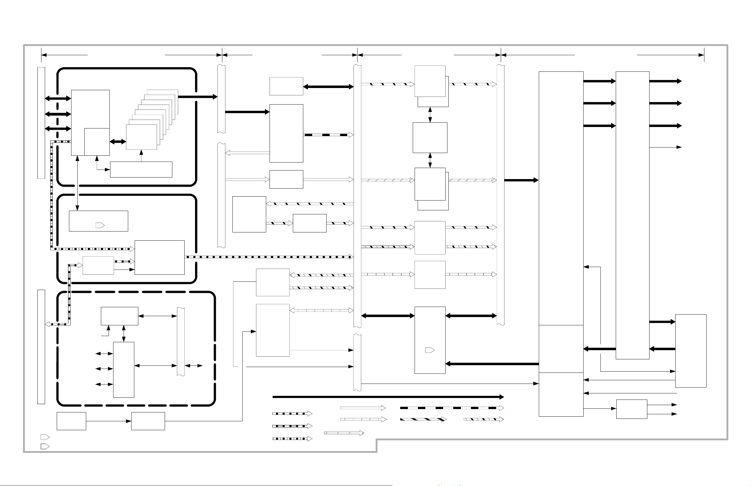
ACQUISITION GROUP PROCESSOR GROUP IMAGE GROUP DISPLAYGROUP
ARRAY FRONT--END
A
R
R
A
Y
S
C
A
N
H
E
A
D
S
RF
SCANHEAD
SELECT
SCANHEAD
SELECT
DAUGHTER
BOARD
MOTOR CONTROLLER
1
CHANNEL
PCB
FRONT--END
CONTROLLER
MECHANICAL
FRONT--END
A
E
C
H
O
B
U
S
GRAYSCALE 2D/
GRAYSCALE 2D/
B
E
C
H
O
B
U
S
ALL
DATATYPES
16 BITS
M--MODE ECHO
8BITS
M--MODE ECHO
COLOR
DATA
PROCESSOR
IMAGE
MEMORY
IF OUTPUT
MODULE
ECHO INPUT
MODULE
ALL DATA TYPES
SPECTRAL, COLOR
DOPPLER
64 BITS
ECHO
COLOR DOPPLER
SPECTRAL
ESTIMATOR
I
M
A
G
E
B
U
S
SPECTRAL/PHYSIO
2D ECH0 2D ECHO
COLOR M--MODE
COLOR
2D SCAN
CONVERTER
ADDRESS
GENERATOR
INTERFACE
SCAN
CONVERTER
DUAL BUFFER
MEMORY
B/W
2D SCAN
CONVERTER
ADDRESS
GENERATOR
INTERFACE
DISPLAY
GRAPHICS
2D COLOR2D COLOR
COLOR M--MODE
SPECTRAL/PHYSIO
V
I
D
E
O
B
U
S
ALL
DATATYPES
ADVANCED
VIDEO
PROCESSOR
VIDEO
”A”
VIDEO
”B”
VIDEO
”C”
VIDEO
MONITORS
EXTERIOR
VIDEO
MONITOR
HARDCOPY
FRAME
SYNC
REAR
PANEL
DOPPLER
ACQUISITION
2D ACQ
(MFE1)
S
T
A
T
I
C
C
W
/
T
C
D
P
R
O
B
E
S
1 Refer to Tables 5C--1and 5C--2 for PCB slot locations.
2
FLOPPY DISK
PHYSIO ECG/PHYSIO
SENSORS
Frame Grabber functions of the Advanced Frame Grabber PCB functional only on systems with 17.X software and up.
INTERFACE
HARD DISK
REPORT
PRINTER
USER
SCS1
RS--232
PHYSIO PHYSIO
I/Q
CONTROL
INTERFACE
CPU
(MFE2)
CONTROL
CONTROL
PREAMP PCB
CONTROL GROUP
C
O
N
T
R
O
L
TO ALL
B
MODULES
U
S
ADVANCED
DIGITAL
DATA
ANALYZER
M--MODE/
PHYSIO
PROCESSOR
(STEERED CW,STATIC CW,STATIC TCD)
STATICCW/STATIC TCD
STEERED CW
PULSED/CW DOPPLER
SPECTRAL DOPPLER
M--MODE ECHO
PHONO AUDIO
DOPPLER AUDIO
2D ECHO
FRAME--GRAB DATA
A
U
D
I
O
B
U
S
ECHO
M--MODE ECHO
M--MODE/PHYSIO M--MODE/PHYSIO
ALL DATA TYPES
MASTER
SCROLLING
GRAPHICS
FRAME
GRABBER
2
COLOR
FRAME--GRAB DATA
VCR VIDEO
AUDIO
DOPPLER
PULSED/CW/SPECTRAL
V
I
D
E
O
B
U
S
VCR
PATH
INTERNAL VCR CONTROL
VCR AUDIO
AUDIO
PATH
AUDIO
BUFFER
PCB
VCR
VIDEO
VCR
VIDEO
PLAYBACK
VCR
MICROPHONE
SPEAKER
PHONES
10 ES01--B03 15
Figure 1A--2. System Signal Path Diagram
(Systems with 7500--0588 or 7500--0677 Motherboards)
HDI-1A-4
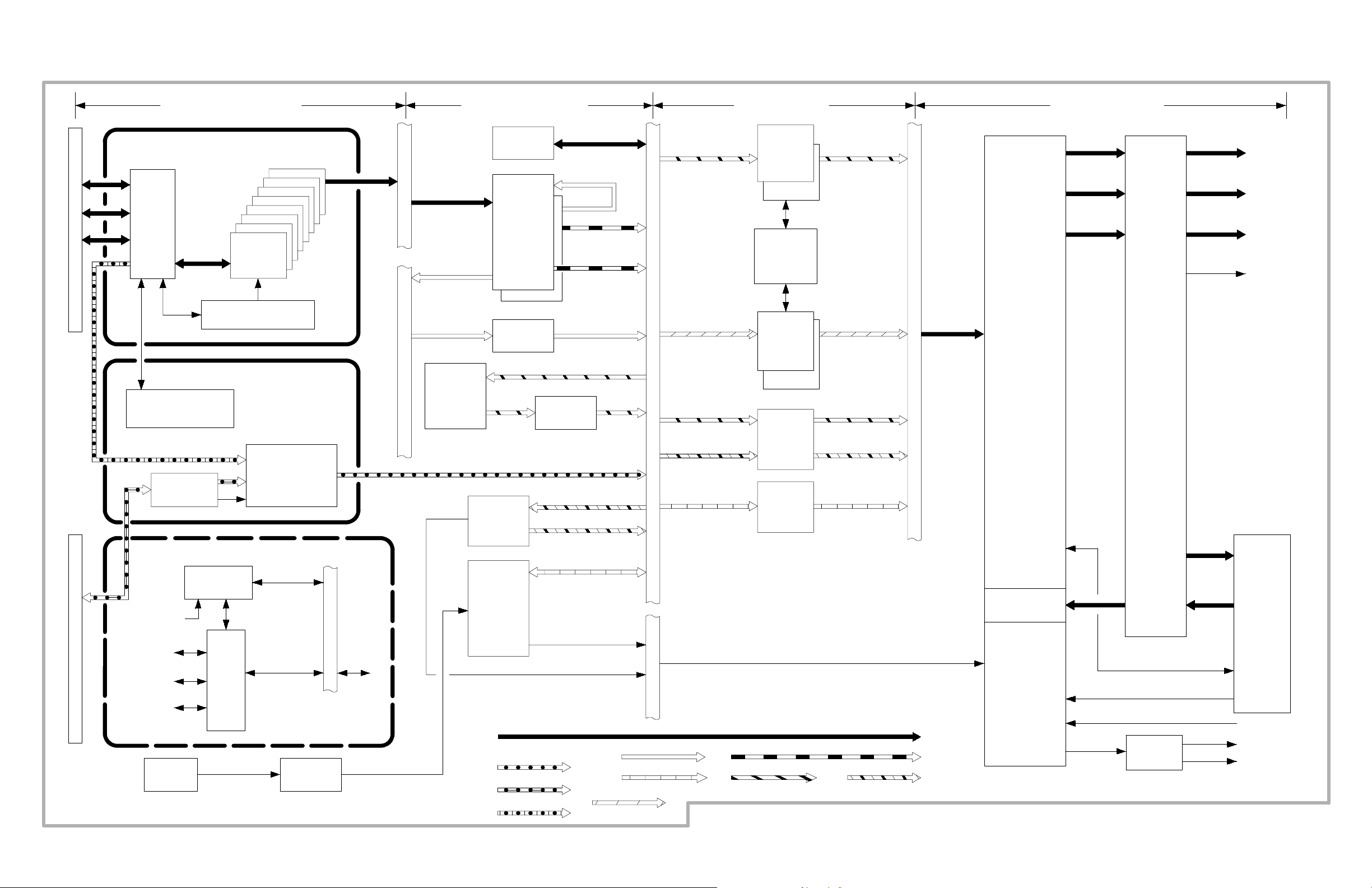
ACQUISITION GROUP PROCESSOR GROUP IMAGE GROUP DISPLAYGROUP
ARRAY FRONT--END
A
R
R
A
Y
S
C
A
N
H
E
A
D
S
RF
SCANHEAD
SELECT
MOTOR CONTROLLER
CHANNEL
PCB
FRONT--END
CONTROLLER
MECHANICAL
FRONT--END
A
E
C
H
O
B
U
S
GRAYSCALE 2D/
GRAYSCALE 2D/
B
E
C
H
O
B
U
S
ALL
DATATYPES
16 BITS
M--MODE ECHO
8BITS
M--MODE ECHO
COLOR
DATA
PROCESSOR
IMAGE
MEMORY
IF OUTPUT
MODULE
MASTER
SLAVE
ECHO INPUT
MODULE
COLOR DOPPLER
ALL DATA TYPES
SPECTRAL, COLOR
SPECTRAL
ESTIMATOR
8BITS
DOPPLER
ECHO
64 BITS
I
M
A
G
E
B
U
S
SPECTRAL/PHYSIO
2D ECH0 2D ECHO
COLOR M--MODE
COLOR
2D SCAN
CONVERTER
ADDRESS
GENERATOR
INTERFACE
SCAN
CONVERTER
DUAL BUFFER
MEMORY
B/W
2D SCAN
CONVERTER
ADDRESS
GENERATOR
INTERFACE
DISPLAY
GRAPHICS
2D COLOR2D COLOR
COLOR M--MODE
SPECTRAL/PHYSIO
V
I
D
E
O
B
U
S
ALL
DATATYPES
ADVANCED
VIDEO
PROCESSOR
A10
VIDEO
”A”
VIDEO
”B”
VIDEO
”C”
VIDEO
MONITORS
EXTERIOR
VIDEO
MONITOR
HARDCOPY
FRAME
SYNC
REAR
PANEL
DOPPLER
ACQUISITION
2D ACQ
(MFE1)
S
T
A
T
I
C
C
W
/
T
C
D
P
R
O
B
E
S
FLOPPY DISK
USER
INTERFACE
HARD DISK
REPORT
PRINTER
SCS1
RS--232
PHYSIO ECG/PHYSIO
SENSORS
I/Q
CONTROL
INTERFACE
CPU
PHYSIO PHYSIO
(MFE2)
CONTROL GROUP
CONTROL
CONTROL
PREAMP PCB
C
O
N
T
R
O
L
B
U
S
TO ALL
MODULES
ADVANCED
DIGITAL
DATA
ANALYZER
M--MODE/
PHYSIO
PROCESSOR
(STEERED CW,STATIC CW,STATIC TCD)
STATICCW/STATIC TCD
STEERED CW
PULSED/CW DOPPLER
SPECTRAL DOPPLER
M--MODE ECHO
PHONO AUDIO
DOPPLER AUDIO
2D ECHO
A
U
D
I
O
B
U
S
ECHO
M--MODE ECHO
M--MODE/PHYSIO M--MODE/PHYSIO
ALL DATA TYPES
MASTER
SCROLLING
GRAPHICS
COLOR
AUDIO
DOPPLER
PULSED/CW/SPECTRAL
VCR
PATH
AUDIO
PATH
INTERNAL VCR CONTROL
VCR AUDIO
AUDIO
BUFFER
PCB
VCR
VIDEO
VCR
VIDEO
PLAYBACK
VCR
MICROPHONE
SPEAKER
PHONES
10 ES01--B14 07
Figure 1A--3. System Signal Diagram (Systems with 7500--0677
Motherboard and Scrolling Graphics Cards only)
HDI--1A--5
ACQUISITION GROUP PROCESSOR GROUP IMAGE GROUP DISPLAY GROUP
ARRAY FRONT--END
A
R
R
A
Y
S
C
A
N
H
E
A
D
S
RF
SCANHEAD
SELECT
MOTOR CONTROLLER
CHANNEL
PCB
FRONT--END
CONTROLLER
MECHANICAL
FRONT--END
A
E
C
H
O
B
U
S
GRAYSCALE 2D/
GRAYSCALE 2D/
B
E
C
H
O
B
U
S
ALL
DATATYPES
16 BITS
M--MODE ECHO
8BITS
M--MODE ECHO
COLOR
DATA
PROCESSOR
IMAGE
MEMORY
IF OUTPUT
MODULE
MASTER
SLAVE
ECHO INPUT
MODULE
COLOR DOPPLER
ALL DATA TYPES
SPECTRAL, COLOR
SPECTRAL
ESTIMATOR
8BITS
DOPPLER
ECHO
64 BITS
I
M
A
G
E
B
U
S
SPECTRAL/PHYSIO
2D ECH0 2D ECHO
COLOR M--MODE
COLOR
2D SCAN
CONVERTER
ADDRESS
GENERATOR
INTERFACE
SCAN
CONVERTER
DUAL BUFFER
MEMORY
B/W
2D SCAN
CONVERTER
ADDRESS
GENERATOR
INTERFACE
2D COLOR2D COLOR
COLOR M--MODE
SPECTRAL/PHYSIO
V
I
D
E
O
B
U
S
ALL
DATATYPES
ADVANCED
VIDEO
PROCESSOR
A10
VIDEO
”A”
VIDEO
”B”
VIDEO
”C”
VIDEO
MONITORS
EXTERIOR
VIDEO
MONITOR
HARDCOPY
FRAME
SYNC
REAR
PANEL
DOPPLER
ACQUISITION
2D ACQ
(MFE1)
S
T
A
T
I
C
C
W
/
T
C
D
P
R
O
B
E
S
FLOPPY DISK
USER
INTERFACE
HARD DISK
REPORT
PRINTER
SCS1
RS--232
PHYSIO ECG/PHYSIO
SENSORS
I/Q
CONTROL
INTERFACE
CPU
PHYSIO PHYSIO
(MFE2)
CONTROL GROUP
CONTROL
CONTROL
PREAMP PCB
C
O
N
T
R
O
L
B
U
S
TO ALL
MODULES
ADVANCED
DIGITAL
DATA
ANALYZER
M--MODE/
PHYSIO
PROCESSOR
(STEERED CW,STATIC CW,STATIC TCD)
STATICCW/STATIC TCD
STEERED CW
PULSED/CW DOPPLER
SPECTRAL DOPPLER
M--MODE ECHO
PHONO AUDIO
DOPPLER AUDIO
2D ECHO
A
U
D
I
O
1
B
U
S
ECHO
M--MODE ECHO
M--MODE/PHYSIO M--MODE/PHYSIO
FRAME--GRAB FRAME--GRAB
DATA
Frame Grabber functions of the Advanced Frame Grabber
PCB functional only on systems with 17.X software and up.
ALL DATA TYPES
ADVANCED
FRAME
GRABBER
COLOR
1
VCR
VIDEO
VCR
VIDEO
PLAYBACK
VCR
MICROPHONE
SPEAKER
PHONES
10 ES01--B15 06
AUDIO
DOPPLER
DATA
VCR VIDEO
PULSED/CW/SPECTRAL
VCR
PATH
AUDIO
PATH
INTERNAL VCR CONTROL
VCR AUDIO
AUDIO
BUFFER
PCB
Figure 1A--4. System Signal Path Diagram (Systems with 7500--0677
Motherboard and Advanced Frame Grabber)
HDI-1A-6
ACQUISITION GROUP PROCESSOR GROUP IMAGE GROUP DISPLAY GROUP
ARRAY FRONT--END
A
R
R
A
Y
S
C
A
N
H
E
A
D
S
RF
S
T
A
T
I
C
C
W
/
T
C
D
P
R
O
B
E
S
SCANHEAD
SELECT
CHANNEL
PCB
FRONT--END
CONTROLLER
MOTOR CONTROLLER
2D ACQ
(MFE1)
USER
INTERFACE
HARD DISK
FLOPPY DISK
REPORT
PRINTER
SCS1
RS--232
PHYSIO ECG/PHYSIO
SENSORS
I/Q
CONTROL
INTERFACE
CPU
PHYSIO PHYSIO
MECHANICAL
FRONT--END
DOPPLER
ACQUISITION
(MFE2)
CONTROL GROUP
CONTROL
CONTROL
PREAMP PCB
C
O
N
T
R
O
L
B
U
S
TO ALL
MODULES
A
E
C
H
O
B
U
S
GRAYSCALE 2D/
GRAYSCALE 2D/
B
E
C
H
O
B
U
S
ALL
DATATYPES
16 BITS
M--MODE ECHO
8BITS
M--MODE ECHO
COLOR
DATA
PROCESSOR
PROCESSOR
(STEERED CW,STATIC CW,STATIC TCD)
IMAGE
MEMORY
IF OUTPUT
MODULE
MASTER
SLAVE
ECHO INPUT
MODULE
COLOR DOPPLER
ADVANCED
DIGITAL
DATA
ANALYZER
M--MODE/
PHYSIO
STATICCW/STATIC TCD
STEERED CW
ALL DATA TYPES
8BITS
SPECTRAL, COLOR
DOPPLER
64 BITS
ECHO
SPECTRAL
ESTIMATOR
PULSED/CW DOPPLER
SPECTRAL DOPPLER
M--MODE ECHO
PHONO AUDIO
DOPPLER AUDIO
2D ECHO
I
M
A
G
E
B
U
S
SPECTRAL/PHYSIO
A
U
D
I
O
B
U
S
ECHO
M--MODE ECHO
2D ECH0 2D ECHO
COLOR M--MODE
M--MODE/PHYSIO M--MODE/PHYSIO
ALL DATA TYPES
COLOR
2D SCAN
CONVERTER
ADDRESS
GENERATOR
INTERFACE
SCAN
CONVERTER
DUAL BUFFER
MEMORY
B/W
2D SCAN
CONVERTER
ADDRESS
GENERATOR
INTERFACE
SCROLLING
GRAPHICS
DISPLAY
COLOR
COLOR M--MODE
SPECTRAL/PHYSIO
AUDIO
DOPPLER
2D COLOR2D COLOR
PULSED/CW/SPECTRAL
V
I
D
E
O
B
U
S
ALL
DATATYPES
ADVANCED
VIDEO
PROCESSOR
A10
VCR
PATH
AUDIO
PATH
VIDEO
”A”
VIDEO
”B”
VIDEO
”C”
INTERNAL VCR CONTROL
REAR
PANEL
VCR AUDIO
AUDIO
BUFFER
PCB
VIDEO
MONITORS
EXTERIOR
VIDEO
MONITOR
HARDCOPY
FRAME
SYNC
VCR
VIDEO
VCR
VIDEO
PLAYBACK
VCR
MICROPHONE
SPEAKER
PHONES
10 ES01--B16 05
Figure 1A--5. System Signal Path Diagram (Systems with 7500--0677
Motherboard and Scrolling Display only)
HDI--1A--7
SCANHEAD SELECT PCB
64/128 ELEMENTS
(LINEAR, CURVED, PHASED)
7 ELEMENTS (ANNULAR)
A
64/128 ELEMENTS
(LINEAR, CURVED, PHASED)
B
C
PERSONALITY
INTERFACE
(ON DAUGHTER BOARD)
FRONT PANEL SCANHEAD CONNECTORS
7 ELEMENTS (ANNULAR)
64/128 ELEMENTS
(LINEAR, CURVED, PHASED)
7 ELEMENTS (ANNULAR)
DATA
MOTOR CONTROLLER PCB
POWER
AMPLIFIER
(4X)
ANALOG FILTER
(PROGRAMMABLE
PROBE
COMPENSATION)
16.5V MOTOR DRIVE
ELEMENT
INTERFACE
(HV MUX)
(IN SCANHEAD)
2
P
O
S
I
T
I
O
N
B
U
S
D/A
CONVERSION
192--
RELAYS
SUBTRACTOR
COMMAND
REGISTER
ENCA
ENCB
ENCZ
POSITION
COUNTER
ANGLE
DETECTOR
CONTROLLER
3
8 CHANNELS
16 ELEMENTS
FOR EACH PCB
ENCODER
PHASE A
PHASE B
MOTOR
CPU
STEERED CW SUMMATION BUS
A23--A29 circuitry is similar to that shown in A22.
DIFFERENTIAL STEERED CW ANALOG SIGNAL
ODD CHNL PCBANALOG TGC
EVEN CHNL PCB ANALOG TGC
2D
ELEMENT 0
1 CHANNEL
(2 ELEMENTS)
ELEMENT 1
ODD CHNL PCB TGC SUM BUS
EVEN CHNL PCB TGC SUM BUS
5
4
3
PULSER PULSER
DIFFERENTIAL
ANALOG TGC
CHANNEL PCB
1
TRANSMIT
RECEIVE
SWITCH
16 T/R/PCB
TRANSMIT
RECEIVE
SWITCH
D/A
CONV.
CW
LOW
2D
TGC/
STEERED
CW
MIXER
ASIC
8/PCB
LO
TRACKING
HIGH VOLTAGE
REGULATORS
(2/PCB)
A/D
8/PCB
8
CONTROL
CHANNEL PCB
CHANNEL PCB
CHANNEL PCB
CHANNEL PCB
CHANNEL PCB
CHANNEL PCB
OUT
A26
SUM
A27
SUM
A28
SUM
A25
SUM
SUM
1/2
FIFO
SUM
ASIC
4/PCB
1/2 DELAY
ASIC CONTROL
4/PCB
PULSER POWER SUPPLY
DIGITAL TGC AND PULSER
CONTROL BUS FROM FEC
BOARD 0
A24
SUM
SUMMED
CHANNELS
TO IFOM
FRONT END
CONTROL BUS
XDCR
TABLE
RAM
120 MHZ
A23
SUM
A22
SUM
FROM OTHER
CHANNEL PCB’S
CHANNEL PCB
BOARD 7
24 MHz SYSTEM CLOCK
A29
IN
1
Refer to Tables 5C--1and 5C--2for PCB slot locations.
2
Summed differential steered CW signals to MFE2
3
Channel PCB 1,3,5,7 analog TGC4
Channel PCB 0,2,4,6 analog TGC
5
FRONT END CONTROLLER PCB
TGC
SEQUENCER
F
R
O
N
T
E
N
D
B
U
S
N
E
T
W
O
R
K
GATE
ARRAY
SEQUENCER
INTER--
PRI
SEQUENCER
INTRA--
PRI
SEQUENCER
MODULE
OPERATION
PROCESSOR
HEADER
GENERATOR
SERIAL
CONTROL
INTERFACE
PROCESSOR
S
Y
S
T
E
M
C
O
N
T
R
O
L
I
N
T
TO/FROM
E
SYSTEM
R
CPU PCB
F
A
C
E
P
R
O
C
E
S
S
O
R
B
U
S
10 ES01--B06 08
Figure 1A--6. Digital Beamformer and Motor Controller Block Diagram
HDI-1A-8
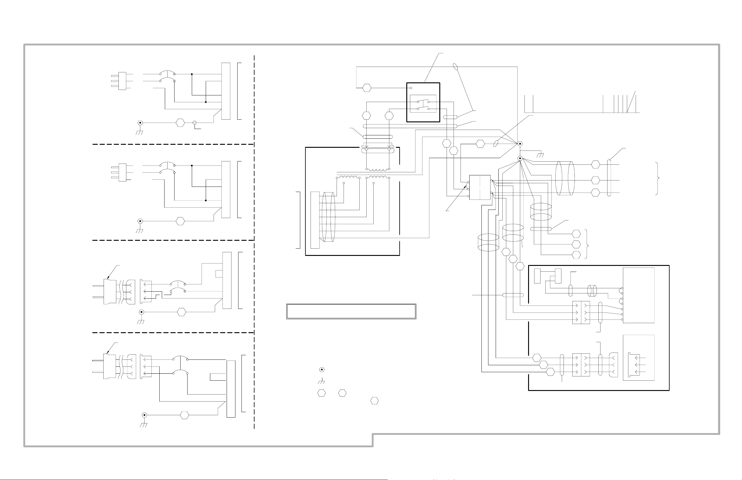
1B Power Distribution
111--24280--02
111--24280--02
POWER CORD
BRN
BLU
GRN/YEL
E4
BRN
BLU
GRN/YEL
E4
E4
MAIN CIRCUIT
BREAKER
12
3
MAIN CIRCUIT
BREAKER
34
1
2
3
1
2
3
4
206
21
206
MAIN CIRCUIT
BREAKER
3
206
MAIN CIRCUIT
BREAKER
1
3
206E4
21
4
2
4
3500--1308--XX
WHT
BLK
GRN/YEL
WHT
BLK
GRN/YEL
P1
1
2
3
4
5
6
7
8
P1
1
2
3
4
5
6
7
8
P1
1
2
3
4
5
6
7
8
P1
1
2
3
4
5
6
7
8
J1
100V
J1
120V
220V
SWITCH = 3300--0283--01
116
107 106
3500--1156--XX
WHT BLK
P1
J1
J1
1
2
3
4
5
6
7
8
(SHIELD)
ISO--XFMR
(2601--0018--01)
AC POWER DISTRIBUTION
J1
NOTES: =GROUND STUD
=
GROUND TO CART WELDMENT
101
T
AND
100
=
TWISTED PAIR WIRE NUMBERS
INSIDE ARE WIRE NUMBERS
GRN/YEL
WHT
BLK
GRN/YEL
GRN/YEL
21 22
11 12
ON/STDBY
SWITCH
GRN/YEL
102
103
9903--0355--01
3500--0767--XX
EM FILTER
5
E
N
1
L
2
(SHIELD)
3500--1156--XX
CONDUIT
110
IN OUT
N
L
ABDI
2/27/91
3500--1305--XX
E2
E3
111
3
4
(SHIELD)
(SHIELD)
3500--1159--XX
208
207
308
307
(SHIELD)
307
209
GRN
BLU
BRN
3500--0897--XX
3500--0766--XX
308
309
3500--0767--XX
309
108
109
TO DIGITAL
POWER SUPPLY
(FIGURE 1B--2)
P/O 3500--0896--XX
(SHIELD)
S. SPEISER
3500--1155--XX
TO TB1, PIN 17
TO TB1, PIN 9
TO TB1, PIN 1
--S
-+
+S
FG
N
H
1700--0016--XX
COLOR
VIDEO
MONITOR
3500--0778--XX
B/W
VIDEO
MONITOR
POWER
SUPPLY
FIGURE 1B--2
MONITOR ASSEMBLY
E = GROUND
240V
10 ES01--B10 05
Figure 1B--1. Power Conversion and Main Power Assy Wiring Diagram
HDI--1B--1
(FOR VCR AND PRINTER POWER CABLES)
3500--1155--XX
DUPLEX RECEPTACLE (115V)
3500--1161--XX
210
212
214
(FIGURE 1B--1)
FROM
LINE FILTER
(FIGURE 1B--1)
(FIGURE 1B--1)
FROM
LINE FILTER
(FIGURE 1B--1)
TO E3
TO E3
111
N
L
108
109
3500--1159--XX
12
56
9
10
13
14
17
18
22
21
TERMINAL BLOCK TB1
(LOCATED IN UPPER PORTION
3500--1123--XX
OF P.S.ASSEMBLY)
3100--1779--XX
4
3
8
7
12
11
16
15
20
19
24
23
3500--1123--XX
FIGURE 1B--3
SHEET 1
3500--1124--XX
FIGURE 1B--3
SHEET 1
2X
N
L
208
207
115V
INPUT
209
LNE
1
203
204
L
115V
INPUT
205
E
N
1
205
204
1
E
115V
INPUT INPUT
504
203
N
505
L
(--S) --6V
514
506
(+S) 6V RTN
507
509
(+S) +6V
(--S) 6V RTN
(+S) +15V
(--S) 15V RTN
218
217
1
ENL
216
510
115V
(--V) --15V
508
511
512
(--V) --16.5V
(+V) 15V RTN
515
513
(+V) +16.5V
(+V) +16.5V RTN
(--V) 16.5V RTN
1 E = GROUND
DIGITAL POWER SUPPLY
(1700--0057--XX, L.H. RESEARCH)
PULSER POWER SUPPLY ASSY
(3500--1131--XX)
1700--0050--XX
1700--0050--XX
1700--0028--XX
1700--0055--XX
1700--0054--XX
1700--0055--XX
ANALOG POWER SUPPLY
10 ES01--B11 01
Figure 1B--2. AC Distribution Wiring Diagram
HDI-1B-2
MB1J1E
MB1J1A
SYSTEM
BACKPLANE
7500--0588--XX
7500--0677--XX
MB1J11A
MB1J11B
+5V SENSE
+5V SENSE RTN
POWER FAIL
123456 10987654321 1234 5678910 10987654321 11 12 13 14 15 16 4321
301
303
304
T301
3500--1215--XX
TO TB2
314
FIGURE 1B--3
SHEET 2
FIGURE 1B--3
SHEET 2
FIGURE 1B--4
3500--1162--XX
”T” numbers indicate the
1
white wire of a twisted
wire pair.
16.5V is supplied to A16/A18 Motor Controller.
2
On systems with the 7500--0677--XX Motherboard, install the Motor Controller PCB only in slot A18
and the Doppler Acquisition PCB (MFE2) only in slot A19.
PIN 8
TO TB2
PIN 14
TO TB2
PIN 2
3500--1304--XX
TO TB2
PIN 18
TO TB2
PIN 6
TO TB2
PIN 12
315
316
350C
352C
351C
202
201
(SHIELD)
(SHIELD)
(SHIELD)
3
1700--0057--XX
L.H. RESEARCH
3500--1212--XX
(BUS BARCABLE)
ENL
DIGITAL P.S.
+5V
--5.2V SENSE
T304
+5V RTN
--5.2V SENSE RTN
N\C
3500--1306--XX
3500--1164--XX
+12V
+12V RTN
+6V
+6V RTN
--6 V
+15V
+15V RTN
--15V
509
510
HV1+
336
--5.2V
T310
1
T310--T311--T312
--12V
--5.2V
--12V RTN
T311
310--311--312
--5.2V RTN
--5.2V
--5.2V RTN
T312
301
1
--5.2V RTN
--5.2V
+5V SENSE
310
--5.2V RTN
311
312
T301
43
2
RTN
N\C
N\C
5V SENSE
303
12V RTN
N\C
314
5
PWR FAIL
--1 2 VDC
+12 VDC
E11 E12 E13
EEEEEEEEEE
316
315
3500--1151--XX
(BUS BARASSEMBLY)
123 456 789
3500--1312--XX
504
505
506
520
514
(+S) +6V
(--S)6V RTN
(+S) 6V RTN
520
1700--0050--XX
1
J1
6
N\C
(--S)--6V
1700--0050--XX
507
(+S) +15V
509
E14
506
505
504
507
Z1
987654321
Z2
510
511
512
508
(--V)--15V
(--S)15V RTN
1700--0028--XX
513
12 515
(--V)--16.5V
(+V) 15V RTN
1700--0054--XX
(+V) +16.5V
(--V) 16.5V RTN
(+V) 16.5V RTN
2
2
1700--0055--XX
1700--0055--XX
HV1 RTN
337
N\C
HV1--
338
3500--1125--XX
32
+48V
--48V RTN
HV2+
HV2 RTN
339
340
1
RTN
48VI
48VI
CHASIS
PULSER P.S.
7500--0589--XX
LAMBDA P.S.
1700--0061--XX
341
GND
HV2--
513
P1
FG
+16.5 VDC
16.5 RTN
511
512
336
337
338
123
RTN
HV +
HV
--16.5 VDC
339
456
HV +
HV --
RTN
HV --
HV
123
340
RTN
HV
HV +
3500--1183--XX
341
3500--1131--XX
PULSER
POWER
SUPPLY ASSY
J3
HV --
SYNC
HVCTRL1
HVCTRL2
DISABLE
4
P4
N\C
P2
1
2
3
4
ANALOG POWER SUPPLY
N\C
N\C
N\C
--5.2V RTN
SENSE
3456
12
J2
N\C
--5.2V SENSE
4
304
T304
HV+ and HV-- are variable from 0 to 105V and depend on the
scanhead type, system type, and mode ofoperation.
Refer to Service Bulletin HDI--30 and Table 3--1.
5
3500--1131--XXcomprises 7500--0589--XX and 1700--0061--XX.
5
3500--1234--XX
PWR SEL
HV CTRL1
3500--1131--XX
4
4
HV CTRL2
CTRL RTN
2275--0285--XX
HV ENABLE0--5V
(FROM SCANHEAD SELECT MODULE)
TO
SCANHEAD
SELECT
MODULE
10 ES01--B08 04
3
E = GROUND
Figure 1B--3. DC Distribution Wiring Diagram (1 of 3)
HDI--1B--3
2100--0538--XX
3500--1304--XX
352C
LOCATED IN UPPER PORTION OF POWER SUPPLY ASSEMBLY
12V DC TERMINAL BLOCK TB2
123
3500--1154--XX3500--1153--XX
--12V
--12V DI G
456
789
314
3500--1306--XX
FROM DIGITAL
POWER
SUPPLY
FIGURE 1B--3
SHEET 1
(SHIELD)
REAR PANEL
DC
FAN
351C
350C
+12
+12V DIG
12V RTN
101112
131415
161718
315
316
TO MB1J1A
FIGURE 1B--3
SHEET 1
10 ES01--B09 01
Figure 1B--3. DC Distribution Wiring Diagram (2 of 3)
HDI-1B-4
SYSTEM BACKPLANE
7500--0588--XX
7500--0677--XX
1--17
1--17
+12V
+12V RTN
MB1J3B
+5V RTN
+5V
+5V
+5V RTN
5678123412 536 6352 43211 4 654
1 234
+12V RTN
DISK
DRIVE
+5V
+5V RTN
+12V
FLOPPY
+12V RTN
+12V
3500--1135--XX
4321
+12V RTN
HARD
DISK
DRIVE
+5V
+5V RTN
+12V
MB1J5 MB1J1B MB1J1C J23
+12V
12V RTN
--12V
+5V
+5V RTN
+12V
ECG PREAMP
DIG GND
1918 20
--12V
2018 19
111--26423--XX
J24
REAR PANEL PCB
--5.2V
(SHIELD) (SHIELD)
3500--0844--XX
635214
--5.2V
+5V RTN
+5V
--12V
12V RTN
346
347
349
345
2536
+12V
GND
CONTROL INTERFACE PCB
348
+12V
P1B
41
+155V
DISPLAY
RETURN
MB1J1D
N\C
N\C
N\C
3500--1303--XX
N\C
N\C
N\C
--12V
12V RTN
+12V
1 23
321
J2
AUDIO BUFFER
REAR PANEL MODULE PCB
7500--0676--XX
3500--0830--XX
3500--0845--XX
B/W
VIDEO
MONITOR
POWER
SUPPLY
1700--0016--XX
+S
+
--
--S
L
H
N
P/O 3500--0896--XX
VIDEO MONITOR ASSEMBLY
+20V
+20V RTN
Figure 1B--3. DC Distribution Wiring Diagram (3 of 3)
10 ES01--B12 01
HDI--1B--5
^J
POWER SUPPLY AREA
3500--1162--XX
DIGITAL POWER
SUPPLY
FIGURE 1B--3
SHEET 1
+12V
--12V
TOP OF CARD CAGE
3500--1109--XX
(TEMP SENSOR)
3500--1221--XX
201
1
1
2
2
P2
202
P2
11
22
3500--1173--XX
P1
1
1
2
2
3443
11
22
P5
P6
+
--
P2
32 1
4
FAN
CONTROLLER
PCB
2100--0679--XX
1(+)
2(--)
P3
+
--
1
P3
4
1
P4
4
2
56
2
5
3
3
6
P4a P4b
+
--
+
--
FANASSEMBLY TRAY
TERMINAL BLOCK TB3
(PART OF 3500--1174--XX)
P7
+
--
3500--1174--XX
P8
+
--
P5
+
--
2100--0386--XX
(6X)
10 ES01--B13 01
Figure 1B--4. Fan Power (DC) Distribution Wiring Diagram
HDI-1B-6

NOTE:
In the following table captions, where there are two slot locations separated by a slash, the slot locations correspond to
the -0588 and -0677 motherboards respectively. Where
there is only one slot location, it corresponds to both motherboards.
Table 1B--1. Power Distribution: A1/A12, A3/A1, A4/A7
Voltage Jack Pins
+5 P1 31A, 31B, 31C
--5.2 30A, 30B
D--GND 27A, 29A, 29B, 29C, 30C, 32A, 32B, 32C
+12 P2 1A, 1B
--12 2A, 2B
D--GND 1C, 2C, 16A, 19C, 21A, 21B, 21C, 28A, 28B, 28C, 32A, 32B,
32C
+5 31A, 31B, 31C
--5.2 25A, 29B
HDI-- 1 B--7

Voltage PinsJack
+5 P3 31A, 31B, 31C
D--GND 32A, 32B, 32C
HDI-- 1 B--8
 Loading...