5 V, 12-Bit nanoDAC, Serial Interface
T
V
FEATURES
8-lead MSOP and 8-lead LFCSP packages
Complete voltage output with internal reference
1 mV/bit with 4.095 V full scale
5 V single-supply operation
No external components required
3-wire serial interface, 20 MHz data loading rate
Low power: 2.5 mW
APPLICATIONS
Portable instrumentation
Digitally controlled calibration
Servo controls
Process control equipment
PC peripherals
in MSOP and LFCSP Packages
AD5626
GENERAL DESCRIPTION
The AD5626, a member of the nanoDAC® family, is a complete
serial input, 12-bit, voltage output digital-to-analog converter
(DAC) designed to operate from a single 5 V supply. It contains
the DAC, input shift register and latches, reference, and a railto-rail output amplifier. The AD5626 monolithic DAC offers
the user low cost and ease of use in 5 V only systems.
Coding for the AD5626 is natural binary with the MSB loaded
first. The output op amp can swing to either rail and is set to a
range of 0 V to 4.095 V for a one-millivolt-per-bit resolution. It
is capable of sinking and sourcing 5 mA. An on-chip reference
is laser trimmed to provide an accurate full-scale output voltage
of 4.095 V.
This part features a serial interface that is high speed, threewire, DSP compatible with data in (SDIN), clock (SCLK), and
load strobe (
connecting multiple DACs.
CLR
The
user demand.
The AD5626 is specified over the extended industrial temperature range (–40°C to +85°C). The AD5626 is available in MSOP
and LFCSP surface-mount packages.
LDAC
). There is also a chip-select pin for
input sets the output to zero scale at power on or upon
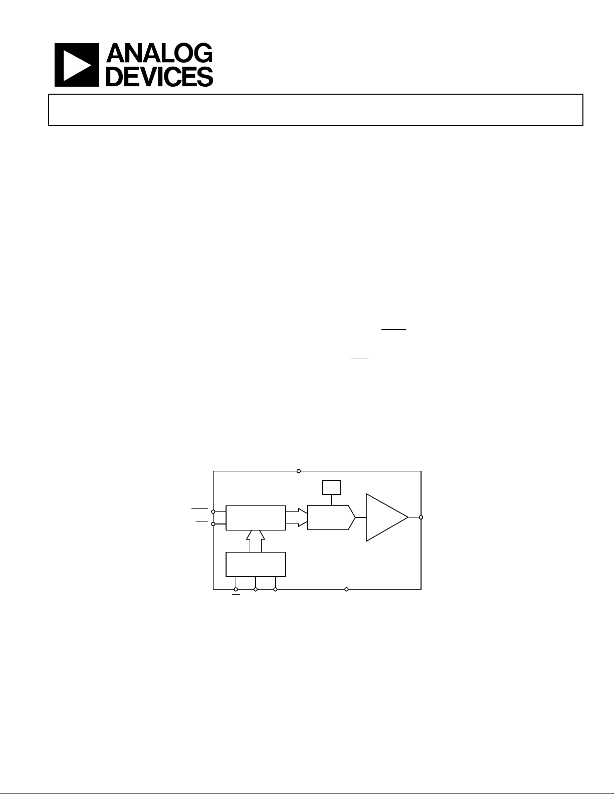
FUNCTIONAL BLOCK DIAGRAM
AD5626
LDAC
CLR
Rev. A
Information furnished by Analog Devices is believed to be accurate and reliable. However, no
responsibility is assumed by Analog Devices for its use, nor for any infringements of patents or other
rights of third parties that may result from its use. Specifications subject to change without notice. No
license is granted by implication or otherwise under any patent or patent rights of Analog Devices.
Trademarks and registered trademarks are the property of their respective owners.
DAC REGISTER
INPUT
REGIS TER
CS SCLK SDIN GND
DD
12-BIT DAC
Figure 1.
REF
OUTPUT
BUFFER
One Technology Way, P.O. Box 9106, Norwood, MA 02062-9106, U.S.A.
Tel: 781.329.4700 www.analog.com
Fax: 781.461.3113 ©2007—2009 Analog Devices, Inc. All rights reserved.
V
OU
06757-001

AD5626
TABLE OF CONTENTS
Features .............................................................................................. 1
Applications ....................................................................................... 1
General Description ......................................................................... 1
Functional Block Diagram .............................................................. 1
Revision History ............................................................................... 2
Specifications ..................................................................................... 3
Electrical Characteristics ............................................................. 3
Timing Characteristics ................................................................ 4
Absolute Maximum Ratings ............................................................ 5
ESD Caution .................................................................................. 5
Pin Configurations and Function Descriptions ........................... 6
Typical Performance Characteristics ............................................. 7
Theory of Operation ...................................................................... 10
DAC Section ................................................................................ 10
Amplifier Section........................................................................ 10
Output Section ............................................................................ 10
Power Supply ............................................................................... 10
Timing and Control ................................................................... 11
Applications Information .............................................................. 12
Power Supplies, Bypassing, and Grounding ........................... 12
Unipolar Output Operation ...................................................... 12
Operating the AD5626 on 12 V or 15 V Supplies Only ........ 13
Measuring Offset Error ............................................................. 13
Bipolar Output Operation ......................................................... 13
Generating a Negative Supply Voltage .................................... 15
A Single-Supply, Programmable Current Source .................. 15
Galvanically-Isolated Interface ................................................. 15
Microprocessor Interfacing ....................................................... 16
Outline Dimensions ....................................................................... 17
Ordering Guide .......................................................................... 17
REVISION HISTORY
1/09—Rev. 0 to Rev. A
Change to Full-Scale Tempco Paramter and Full-Scale
Voltage (Min) Parameter ................................................................. 3
12/07—Revision 0: Initial Version
Rev. A | Page 2 of 20

AD5626
SPECIFICATIONS
ELECTRICAL CHARACTERISTICS
@ VDD = 5.0 V ± 5%, −40°C ≤ TA ≤ +85°C, B grade device, unless otherwise noted.
Table 1.
Parameter Symbol Condition Min Typ Max Unit
STATIC PERFORMANCE
Resolution N 12 Bits
Relative Accuracy INL −1 ±1/4 +1 LSB
Differential Nonlinearity DNL No missing codes −1 ±3/4 +1 LSB
Zero-Scale Error V
Full-Scale Voltage VFS Data = 0xFFF1 4.079 4.095 4.111 V
Full-Scale Tempco
2, 3
TCVFS 20 ppm/°C
ANALOG OUTPUT
Output Current I
Load Regulation at Midscale L
Capacitive Load CL No oscillation2 500 pF
LOGIC INPUTS
Logic Input
Low Voltage VIL 0.8 V
High Voltage VIH 2.4 V
Input Leakage Current IIL 10 μA
Input Capacitance CIL 10 pF
AC CHARACTERISTICS2
Voltage Output Settling Time tS To ±1 LSB of final value3 16 μs
DAC Glitch 15 nV-s
Digital Feedthrough 15 nV-s
SUPPLY CHARACTERISTICS
Positive Supply Current IDD VIH = 2.4 V, VIL = 0.8 V, no load 1.5 2.5 mA
V
Power Dissipation P
V
Power Supply Sensitivity PSS ΔVDD = ±5% 0.002 0.004 %/%
1
Includes internal voltage reference error.
2
These parameters are guaranteed by design and not subject to production testing.
3
The settling time specification does not apply for negative going transitions within the last 6 LSBs of ground. Some devices exhibit double the typical settling time in
this 6 LSB region.
Data = 0x000 1/2 3 LSB
ZSE
Data = 0x800 ±5 ±7 mA
OUT
RL = 402 Ω to ∞, data = 0x800 1 3 LSB
REG
= 5 V, VIL = 0 V, no load 0.5 1 mA
DD
V
DISS
= 2.4 V, VIL = 0.8 V, no load 7.5 12.5 mW
IH
= 5 V, VIL = 0 V, no load 2.5 5 mW
DD
Rev. A | Page 3 of 20

AD5626
V
TIMING CHARACTERISTICS
@ VDD = 5.0 V ± 5%, −40°C ≤ TA ≤ +85°C, unless otherwise noted.
Table 2.
Parameter
tCH 30 ns min Clock width high
tCL 30 ns min Clock width low
t
LDW
tDS 15 ns min Data setup
t
15 ns min Data hold
DH
t
CLRW
t
15 ns min Load setup
LD1
t
10 ns min Load hold
LD2
t
30 ns min Select
CSS
t
CSH
1
These parameters are guaranteed by design and not subject to production testing.
2
All input control signals are specified with tr = tf = 5 ns (10% to 90% of 5 V) and timed from a voltage level of 1.6 V.
Timing Diagram
1, 2
Limit at T
MIN
, T
Unit Description
MAX
20 ns min Load pulse width
30 ns min Clear pulse width
20 ns min Deselect
OUT
SDIN
SCLK
CS
LDAC
SDIN
SCLK
LDAC
CLR
FS
ZS
D11 D10 D9 D8 D7 D6 D5 D4
t
CSS
t
LD1
t
t
DS
t
CL
DH
t
CH
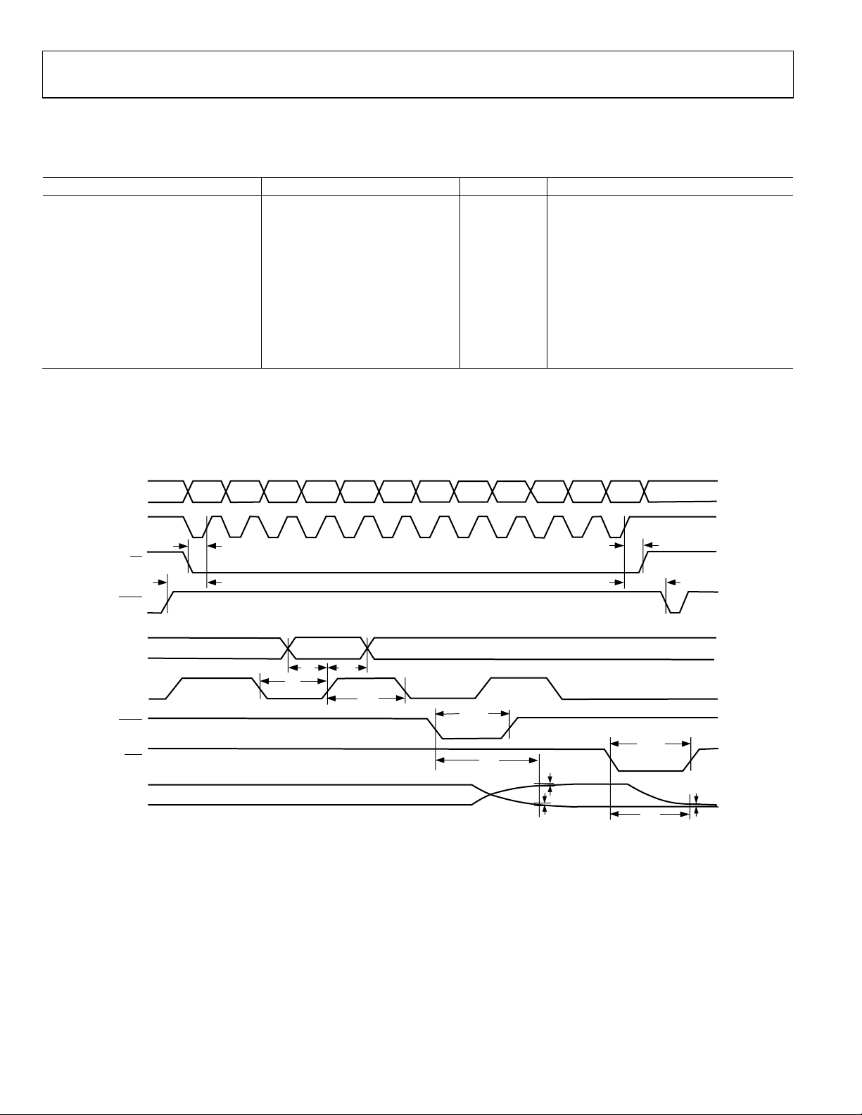
Figure 2. Timing Diagram
t
D3 D2 D1 DO
LDW
t
S
±1 LSB
ERROR BAND
t
LD2
t
CLRW
t
CSH
t
S
06757-002
Rev. A | Page 4 of 20

AD5626
ABSOLUTE MAXIMUM RATINGS
Table 3.
Parameter Rating
VDD to GND −0.3 V to +10 V
Logic Inputs to GND −0.3 V to VDD + 0.3 V
V
to GND −0.3 V to VDD + 0.3 V
OUT
I
Short Circuit to GND 50 mA
OUT
Package Power Dissipation (TJ max − TA)/θJA
Thermal Resistance (θJA)
8-Lead MSOP 220°C/W
8-Lead LFCSP 62°C/W
Maximum Junction Temperature
max)
(T
J
Operating Temperature Range −40°C to +85°C
Storage Temperature Range −65°C to +150°C
Lead Temperature JEDEC industry standard
Soldering J-STD-020
150°C
Stresses above those listed under Absolute Maximum Ratings
may cause permanent damage to the device. This is a stress
rating only; functional operation of the device at these or any
other conditions above those indicated in the operational
section of this specification is not implied. Exposure to absolute
maximum rating conditions for extended periods may affect
device reliability.
ESD CAUTION
Rev. A | Page 5 of 20

AD5626
PIN CONFIGURATIONS AND FUNCTION DESCRIPTIONS
V
CS
SCLK
SDIN
DD
1
AD5626
2
TOP VIEW
3
(Not to Scal e)
4
8
7
6
5
V
OUT
GND
CLR
LDAC
V
1
DD
2
3
(Not to Scale)
4
AD5626
TOP VIEW
CS
SCLK
6757-003
SDIN
8
7
6
5
V
OUT
GND
CLR
LDAC
6757-004
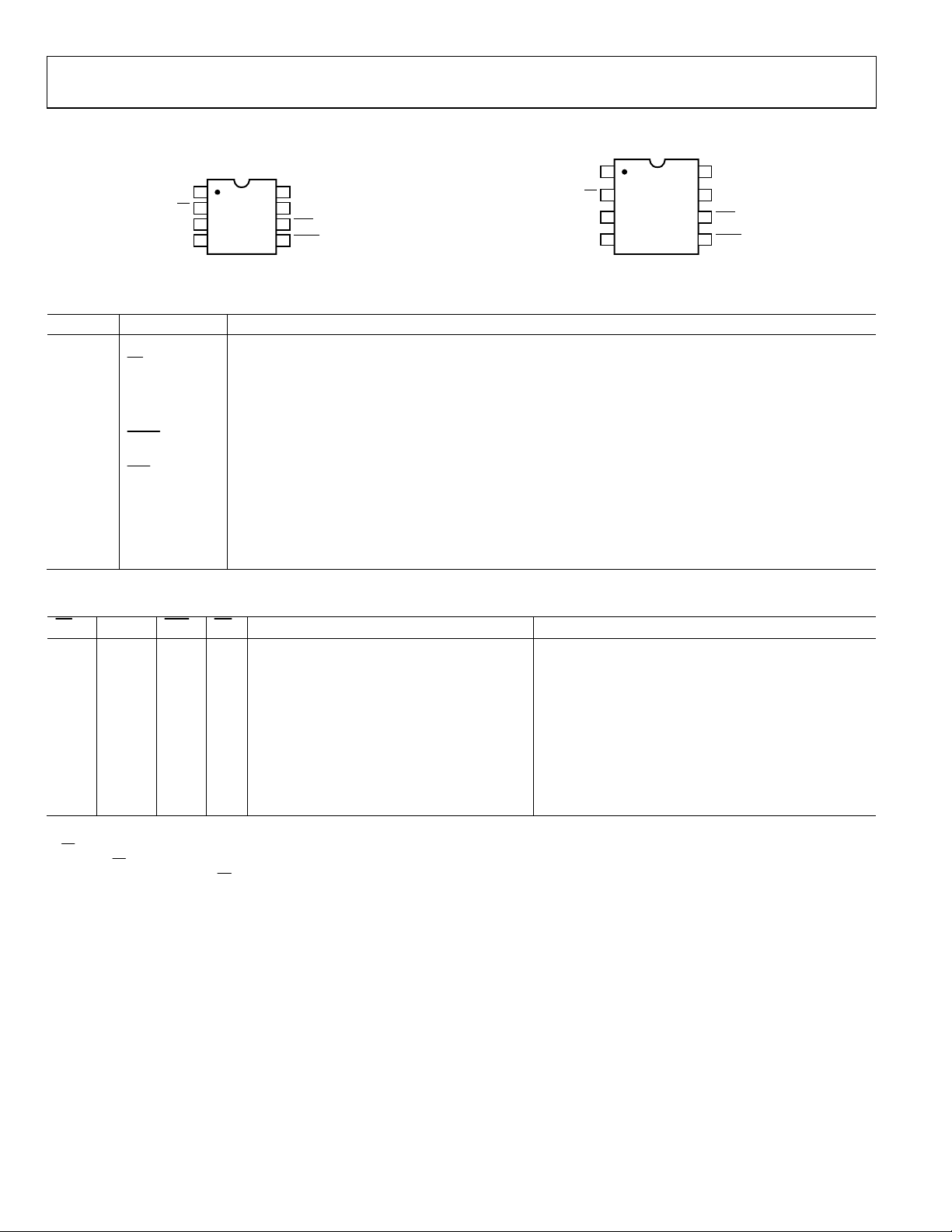
Figure 3. 8-Lead MSOP Pin Configuration Figure 4. 8-Lead LFCSP Pin Configuration
Table 4. Pin Function Descriptions
Pin No. Mnemonic Description
1 VDD Positive Supply. Nominal value 5 V ± 5%.
2
CS
Chip Select. Active low input.
3 SCLK Clock Input. Clock input for the internal serial input shift register.
4 SDIN
Serial Data Input. Data on this pin is clocked into the internal serial register on positive clock edges of the
SCLK pin. The most significant bit (MSB) is loaded first.
5
Serial Register Data Write to DAC Register. Active low input that writes the serial register data into the DAC
LDAC
register. Asynchronous input.
6
Clear DAC Register. Active low digital input that clears the DAC register to zero, setting the DAC to minimum
CLR
scale. Asynchronous input.
7 GND Ground. Analog ground for the DAC. This also serves as the digital logic ground reference voltage.
8 V
OUT
Voltage Output from the DAC. Fixed output voltage range of 0 V to 4.095 V with 1 mV/LSB. An internal
temperature stabilized reference maintains a fixed full-scale voltage independent of time, temperature, and
power supply variations.
Table 5. Control Logic Truth Table1
CS
2, 3
2
CLK
CLR
LD
4
Serial Shift Register Function DAC Register Function
H X H H No effect Latched
L L H H No effect Latched
L H H H No effect Latched
L
↑+
↑+
L H H Shift-register-data advanced one bit Latched
H X H
H H Shift-register-data advanced one bit Latched
No effect Updated with current shift register contents
↓–
H X H L No effect Transparent
H X L X No effect Loaded with all zeros
H X
1
↑+ indicates a positive logic transition; ↓– indicates a negative logic transition; X = don’t care.
2
CS and CLK are interchangeable.
3
Returning CS high avoids an additional false clock of serial data input.
4
Do not clock in serial data while LD is low.
↑+
H No effect Latched all zeros
Rev. A | Page 6 of 20
 Loading...