a
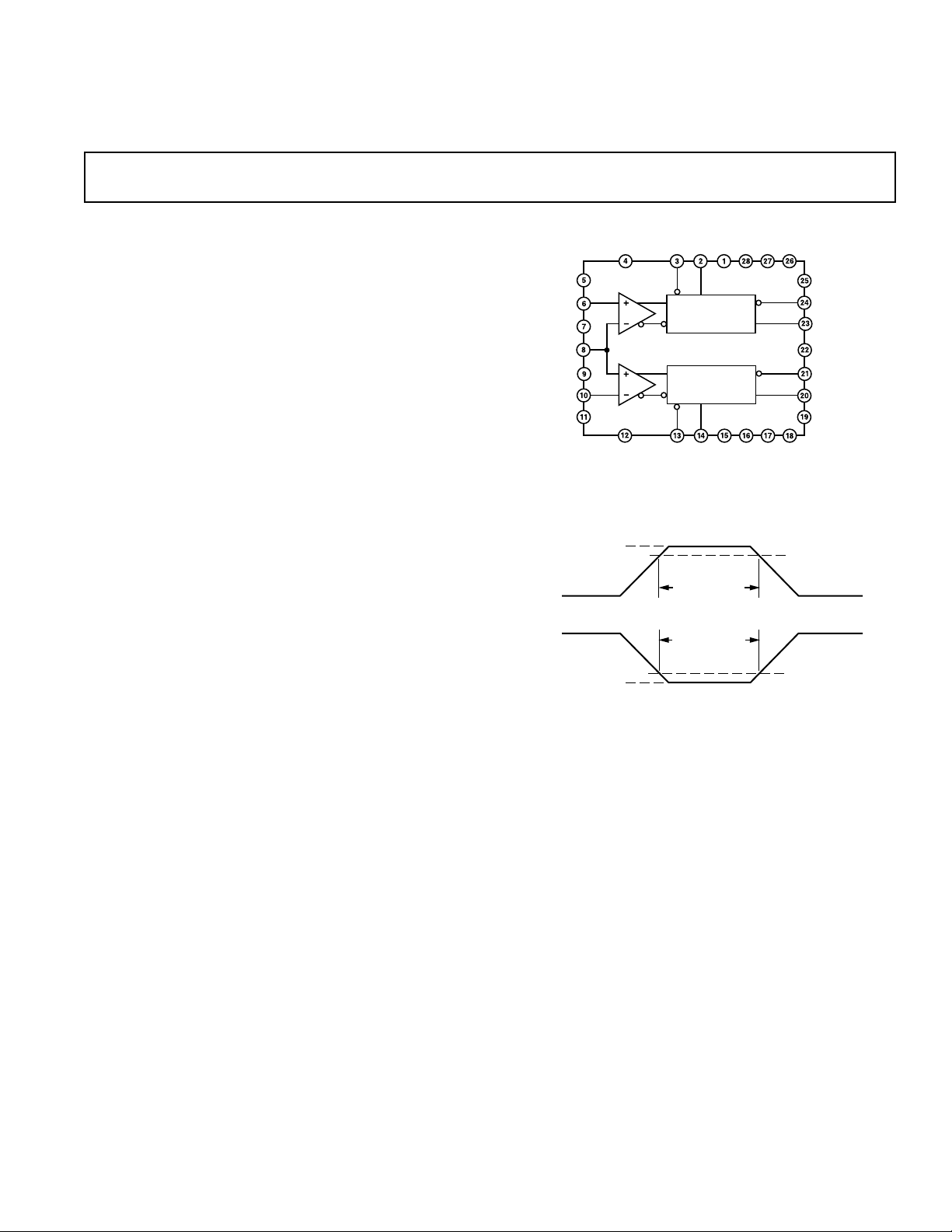
2.8V
0.2V
3.0V
0V
0V
3.0V
MIN. POSITIVE
INPUT PULSE
MIN. NEGATIVE
INPUT PULSE
High Speed Window Comparator
AD53042
FEATURES
–2 V to +7 V Input Voltage Range
Low V
Bias Current (<100 nA)
IN
Up to 5 V/ns Input Signal Tracking
Low Dispersion of ⴞ100 ps
28-Lead PLCC Package
APPLICATIONS
Automatic Test Equipment
Semiconductor Test Systems
Board Test Systems
PRODUCT DESCRIPTION
The AD53042 is an ultrahigh speed window comparator
with latch. It uses a high speed monolithic process to provide
high dc accuracy without sacrificing input voltage range.
On-chip connection of the common input eliminates the
contributions of a second bonding pad and package pin to
the input capacitance, resulting in a maximum input
capacitance of 2 pF.
The AD53042 employs a high precision differential input
stage with a common mode range of 9 V. Its complementary
digital outputs are fully ECL-compatible. The output stage is
capable of driving a 50 Ω line terminated to –2 V. The device
also provides a latch function, allowing operation in track-hold
mode and can also be used to generate hysteresis.
FUNCTIONAL BLOCK DIAGRAM
GND
GND
V
A
NC
V
IN
NC
V
B
GND
NOTE:
NOT THE ACTUAL PHYSICAL LAYOUT OF DEVICE.
NC = NO CONNECTION INSIDE PACKAGE.
LEA
LATCH/OUTPUT
AD53042
LATCH/OUTPUT
LEB
LEA NC
A
B
LEB
NC
+V
S
–V
NC GNDGND
Figure 1. Typical Application Circuit
NC
GND
GND
QA
QA
DGND
QB
QB
GND
S
REV. A
Information furnished by Analog Devices is believed to be accurate and
reliable. However, no responsibility is assumed by Analog Devices for its
use, nor for any infringements of patents or other rights of third parties
which may result from its use. No license is granted by implication or
otherwise under any patent or patent rights of Analog Devices.
One Technology Way, P.O. Box 9106, Norwood, MA 02062-9106, U.S.A.
Tel: 781/329-4700 World Wide Web Site: http://www.analog.com
Fax: 781/326-8703 © Analog Devices, Inc., 1999

(All specifications apply with TC = 40ⴗC to 100ⴗC and +VS = +7.75 V to +11.5 V;
AD53042–SPECIFICATIONS
–VS = –3.95 V to –7.7 V unless otherwise noted.)
Parameter Min Typ Max Units Test Conditions
POWER SUPPLIES
Positive Supply Currents 65 mA No Load
Negative Supply Current –85 mA No Load
Power Dissipation 1.19 W No Load, +VS = +10 V, –VS = –5.2 V
DC INPUT CHARACTERISTICS
Offset Voltage (V
Bias Current –0.5 <0.1 0.5 µAV
V
IN
, V
Bias Current –20 20 µAV
V
A
B
Capacitance V
Voltage Range (V
Differential Voltage (V
) –10 10 mV CMV = 0 V
OS
, VA, V
IN
B
)–V
CM
)9V
DIFF
+ 2.7 +VS – 2.5 V
S
2pF
= 0 V
IN
= 0 V
IN
Nonlinearity –5 5 mV See Note 1
VA/VB Interaction 0.1 mV/V
BIAS CURRENT
Change vs. Comparator State –1 1 µA
Nonlinearity –2 2 µA
Tempco ±0.1 µA/°C
LATCH ENABLE INPUTS
Common-Mode Range –2 1 V
Differential Voltage 0.4 3 V
Logic “1” Current (L
Logic “0” Current (L
) 200 µA
IH
) –10 µA
IL
DIGITAL OUTPUTS
Logic “1” Voltage (V
Logic “0” Voltage (V
) –0.98 V Q or Q, 50 Ω to –2 V
OH
) –1.5 V Q or Q, 50 Ω to –2 V
OL
SWITCHING PERFORMANCE
Propagation Delay
Input to Output 2 ns V
= 2 V p-p, t
IN
PDR
, t
, Figure 1, Note 2
PDF
Latch Enable to Output 1.2 ns
Part-to-Part Skew 1 ns
Change vs. Temperature ±1 ps/°C
DISPERSION
5 V p-p Input (All Edges) ±100 ps 10%, 90% 0.5 V/ns, 3 V/ns
5 V p-p Input (All Edges) ±175 ps 10%, 90% 5 V/ns
V Slew = 1 V/ns (All Edges) ±50 ps 10%, 90% 3 V, 5 V
V Slew = 1 V/ns (All Edges) ±50 ps 20%, 80% 1 V
Minimum Pulsewidth <1 ns See Note 3
Edge Interaction <200 ps See Note 4
Duty Ratio <100 ps See Note 5
Comparator Interaction <100 ps
NOTES
1
Defined as change in VOS from –VS + 2.95 V to +VS – 2.75 V (throughout the range) after VA and VB are corrected for gain and offset using 0 V and 5 V.
2
Propagation delay is measured from the input threshold crossing at the 50% point of a 0 V to 5 V input to the output Q and Q crossing.
3
The minimum input pulsewidth that will maintain a 600 mV ECL swing on the output. The input is a 0 V to 3 V signal with a 3 V/ns rise and fall times. The input
pulsewidth is measured between the 2.8 V point of a positive input pulse and the 0.2 V of a negative input pulse. See Figure 2.
4
Maximum Change in propagation delay as the input pulse is reduced from 50 ns to a 2 ns pulsewidth. 0 V to 3 V swing with 3 V/ns rise/fall time and 25% duty cycle.
5
Maximum Change in propagation delay as the input pulse is reduced from 99% to a 1% duty cycle. 0 V to 3 V swing with 3 V/ns rise/fall time and 50 ns to 4.95 µs
pulsewidth, period = 5 µs.
Specifications subject to change without notice.
–2–
REV. A
 Loading...