

Single/Dual, +15 V/±5 V, 256-Position,
A
S
A
www.BDTIC.com/ADI
I2C-Compatible Digital Potentiometer
FEATURES
AD5280: 1 channel
AD5282: 2 channels
256 positions
5 V to 15 V single supply; ±5.5 V dual-supply operation
Fixed terminal resistance: 20 kΩ, 50 kΩ, 200 kΩ
Low temperature coefficient: 30 ppm/°C
Power-on midscale preset
Programmable reset
Operating temperature: −40
2
I
C-compatible interface
APPLICATIONS
Multimedia, video, and audio
Communications
Mechanical potentiometer replacement
Instrumentation: gain, offset adjustment
Programmable voltage source
Programmable current source
Line impedance matching
GENERAL DESCRIPTION
The AD5280/AD5282 are single-channel and dual-channel,
256-position, digitally controlled variable resistors (VRs)
The devices perform the same electronic adjustment function
as a potentiometer, trimmer, or variable resistor. Each VR offers
a completely programmable value of resistance between the
A terminal and the wiper or the B terminal and the wiper. The
fixed A-to-B terminal resistance of 20 kΩ, 50 kΩ, or 200 kΩ has
a 1% channel-to-channel matching tolerance. The nominal
temperature coefficient of both parts is 30 parts per million/
degrees centigrade (ppm/°C). Another key feature is that the
parts can operate up to +15 V or ±5 V.
Wiper position programming defaults to midscale at system
wer-on. When powered, the VR wiper position is programmed
po
2
by an I
C-compatible, 2-wire serial data interface. The AD5280/
AD5282 feature sleep mode programmability. This allows any
level of preset in power-up and is an alternative to a costly
EEPROM solution. Both parts have additional programmable
1
Assert shutdown and program the device during power-up, then deassert
the shutdown to achieve the desired preset level.
2
The terms digital potentiometer, VR, and RDAC are used interchangeably.
1
o
C to +85oC
2
.
AD5280/AD5282
logic outputs that enable users to drive digital loads, logic gates,
LED drivers, and analog switches in their system.
The AD5280/AD5282 are available in thin, surface-mounted
14-lead TSSOP and 16-lead TSSOP. All parts are guaranteed to
operate over the extended industrial temperature range of
−40°C to +85°C. For 3-wire SPI-compatible interface applications, see the
w.analog.com.
ww
SHDN
V
V
DD
DD
V
V
SS
SCL
SDA
GND
AD5260/AD5262 product information on
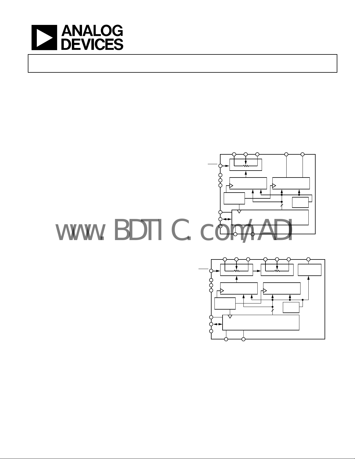
FUNCTIONAL BLOCK DIAGRAMS
WB O1O
HDN
V
DD
V
L
V
SS
SCL
SDA
GND
L
RDAC REGISTER OUTPUT REG ISTER
ADDRESS
CODE
SERIAL INPUT REGISTER
AD0 AD1
Figure 1. AD5280
1W1B1
RDAC1 REGISTE R RDAC2 REGISTE R
ADDRESS
CODE
SERIAL INPUT REGISTER
AD0 AD1
A2W2B
8
Figure 2. AD5282
PWR ON
8
2
PWR ON
RESET
2
RESET
AD5280
OUTPUT
REGIS TER
AD5282
02929-070
O
1
02929-001
Rev. B
Information furnished by Analog Devices is believed to be accurate and reliable. However, no
responsibility is assumed by Anal og Devices for its use, nor for any infringements of patents or ot her
rights of third parties that may result from its use. Specifications subject to change without notice. No
license is granted by implication or otherwise under any patent or patent rights of Analog Devices.
Trademarks and registered trademarks are the property of their respective owners.
One Technology Way, P.O. Box 9106, Norwood, MA 02062-9106, U.S.A.
Tel: 781.329.4700 www.analog.com
Fax: 781.461.3113 ©2002–2007 Analog Devices, Inc. All rights reserved.

AD5280/AD5282
www.BDTIC.com/ADI
TABLE OF CONTENTS
Features.............................................................................................. 1
Applications....................................................................................... 1
General Description ......................................................................... 1
Functional Block Diagrams............................................................. 1
Revision History ............................................................................... 2
Specifications..................................................................................... 3
Electrical Characteristics ............................................................. 3
Absolute Maximum Ratings............................................................ 5
Thermal Resistance ...................................................................... 5
ESD Caution.................................................................................. 5
Pin Configurations and Function Descriptions ........................... 6
Typical Performance Characteristics ............................................. 7
Test Circuits..................................................................................... 12
Theory of Operation ...................................................................... 14
Rheostat Operation .................................................................... 14
Potentiometer Operation........................................................... 14
Digital Interface .............................................................................. 16
2-Wire Serial Bus........................................................................ 16
Readback RDAC Value ..............................................................17
Additional Programmable Logic Output ................................ 17
Self-Contained Shutdown Function and Programmable
Preset............................................................................................ 17
Multiple Devices on One Bus ................................................... 17
Level Shift for Bidirectional Interface...................................... 18
Level Shift for Negative Voltage Operation ............................ 18
ESD Protection ........................................................................... 18
Terminal Voltage Operating Range ......................................... 18
Power-Up Sequence................................................................... 18
Layout and Power Supply Bypassing ....................................... 19
Applications Information.............................................................. 20
Bipolar DC or AC Operation from Dual Supplies................. 20
Gain Control Compensation.................................................... 20
15 V, 8-Bit I2C DAC.................................................................... 20
8-Bit Bipolar DAC...................................................................... 21
Bipolar Programmable Gain Amplifier................................... 21
Programmable Voltage Source with Boosted Output ........... 21
Programmable Current Source ................................................ 22
Programmable Bidirectional Current Source......................... 22
Programmable Low-Pass Filter ................................................ 23
Programmable Oscillator.......................................................... 23
RDAC Circuit Simulation Model............................................. 24
Macro Model Net List for RDAC............................................. 24
Outline Dimensions....................................................................... 25
Ordering Guide .......................................................................... 26
REVISION HISTORY
8/07—Rev. A to Rev. B
Updated Operating Temperature Range Throughout...................1
hanges to the Features Section .......................................................1
C
Changes to the General Description Section..................................1
Changes to Table 2..............................................................................3
Added the Thermal Resistance Section...........................................5
Changes to the Ordering Guide......................................................26
11/05—Rev. 0 to Rev. A
Updated Format................................................................... Universal
Updated Outline Dimensions.........................................................26
Changes to Ordering Guide............................................................27
10/02—Revision 0: Initial Version
Rev. B | Page 2 of 28

AD5280/AD5282
www.BDTIC.com/ADI
SPECIFICATIONS
ELECTRICAL CHARACTERISTICS
VDD = +15 V, VSS = 0 V or VDD = +5 V, VSS = −5 V; V
= 5 V, VA = +VDD, VB = 0 V; −40°C < TA < +85°C, unless otherwise noted.
LOGIC
Table 1.
Parameter Symbol Conditions Min Typ
DC CHARACTERISTICS–RHEOSTAT MODE
Resistor Differential NL
Resistor Nonlinearity
Nominal Resistor Tolerance
Resistance Temperature
Coefficient
Wiper Resistance R
2
2
R-DNL RWB, VA = NC −1 ±1/4 +1 LSB
R-INL RWB, VA = NC −1 ±1/4 +1 LSB
3
ΔR
T
AB
(∆RAB/RAB)/∆T x 10
I
W
DC CHARACTERISTICS–POTENTIOMETER DIVIDER MODE (specifications apply to all VRs)
Resolution N
Integral Nonlinearity
Differential Nonlinearity
Voltage Divider Temperature
4
4
INL
DNL
(∆V
)/∆T x 106 Code = 0x80
W/VW
= 25°C −30
A
6
VAB = VDD, wiper = no connect
= VDD/R, VDD = 3 V or 5 V
W
30
60 150 Ω
8
−1 ±1/4 +1 LSB
−1 ±1/4 +1 LSB
5
Coefficient
Full-Scale Error V
Zero-Scale Error V
RESISTOR TERMINALS
Voltage Range
Capacitance A, B
Capacitance W
5
6
6
Common-Mode Leakage I
Shutdown Current I
DIGITAL INPUTS AND OUTPUTS
Input Logic High V
Input Logic Low V
Output Logic High (O1, O2) V
Output Logic Low (O1, O2) V
Input Current I
Input Capacitance
6
POWER SUPPLIES
Logic Supply V
Power Single-Supply Range V
Power Dual-Supply Range V
Logic Supply Current I
Positive Supply Current I
Negative Supply Current I
Power Dissipation
7
Power Supply Sensitivity PSS
DYNAMIC CHARACTERISTICS
6, 8 , 9
Bandwidth −3 dB BW_20K RAB = 20 kΩ, Code = 0x80
Code = 0xFF −2 −1 0 LSB
WFSE
Code = 0x00 0 +1 +2 LSB
WZSE
VA, VB, V
CA, C
C
CM
SHDN
W
B
W
V
V
f = 5 MHz, measured to GND,
Code = 0x80
f = 1 MHz, measured to GND,
Code = 0x80
= VB = V
A
W
SS
25
55
1
IH
IL
IH
IL
V
IL
C
IL
0.7 × VL
0
4.9
= 0 V or 5 V
IN
5
LOGI C
V
DD RANGE
DD/SS RANGE
LOGI C
DD
SS
P
DISS
V
V
= 0 V 4.5
SS
= 5 V
LOGI C
= 5 V or VIL = 0 V
IH
2.7
±4.5
VIH = 5 V or VIL = 0 V, VDD = +5 V, VSS = −5
V
0.1 1 μA
0.1 1 μA
0.2 0.3 mW
0.002 0.01 %/%
310
150
35
BW_50K RAB = 50 kΩ, Code = 0x80
BW_200K RAB = 200 kΩ, Code = 0x80
1
Max Unit
+30 %
V
V
DD
5 μA
VL + 0.5 V
0.3 × VL V
0.4 V
±1 μA
VDD V
16.5 V
±5.5 V
60 μA
ppm/°C
Bits
ppm/°C
pF
pF
nA
V
pF
kHz
kHz
kHz
Rev. B | Page 3 of 28
AD5280/AD5282
S
www.BDTIC.com/ADI
Parameter Symbol Conditions Min Typ
Total Harmonic Distortion THD
VW Settling Time t
Crosstalk CT
V
W
V
S
= 1 V rms, RAB = 20 kΩ
A
VB = 0 V dc, f = 1 kHz
= 5 V, VB = 5 V, ±1 LSB error band
A
= VDD, VB = 0 V, measure VW1 with
V
A
0.014
5
15
1
Max Unit
%
μs
nV-s
adjacent RDAC making full-scale
code change
Analog Crosstalk CTA
Measure V
10 kHz
Resistor Noise Voltage e
INTERFACE TIMING CHARACTERISTICS (applies to all parts)
SCL Clock Frequency f
t
Bus Free Time Between
BUF
Stop and Start
t
Hold Time (Repeated
HD:STA
Start)
t
Low Period of SCL Clock t3
LOW
t
High Period of SCL Clock t4
HIGH
t
Setup Time for Start
SU:STA
Condition
t
Data Hold Time t6
HD:DAT
t
Data Setup Time t7
SU:DAT
tF Fall Time of Both SDA and
SCL Signals
tR Rise Time of Both SDA and
SCL Signals
t
Setup Time for STOP
SU:STO
Condition
1
Typicals represent average readings at 25°C, VDD = +5 V, VSS = −5 V.
2
Resistor position nonlinearity error R-INL is the deviation from an ideal value measured between the maximum resistance and the minimum resistance wiper
positions. R-DNL measures the relative step change from ideal between successive tap positions. Parts are guaranteed monotonic.
3
VAB = VDD, wiper (VW) = no connect.
4
INL and DNL are measured at VW with the RDAC configured as a potentiometer divider similar to a voltage output DAC. VA = VDD and VB = 0 V. DNL specification limits
of ±1 LSB maximum are guaranteed monotonic operating conditions.
5
Resistor Terminal A, Resistor Terminal B, and Wiper Terminal W have no limitations on polarity with respect to each other.
6
Guaranteed by design and not subject to production test.
7
P
is calculated from (IDD × VDD). CMOS logic level inputs result in minimum power dissipation.
DISS
8
Bandwidth, noise, and settling time are dependent on the terminal resistance value chosen. The lowest R value results in the fastest settling time and highest
bandwidth. The highest R value results in the minimum overall power consumption.
9
All dynamic characteristics use VDD = 5 V.
10
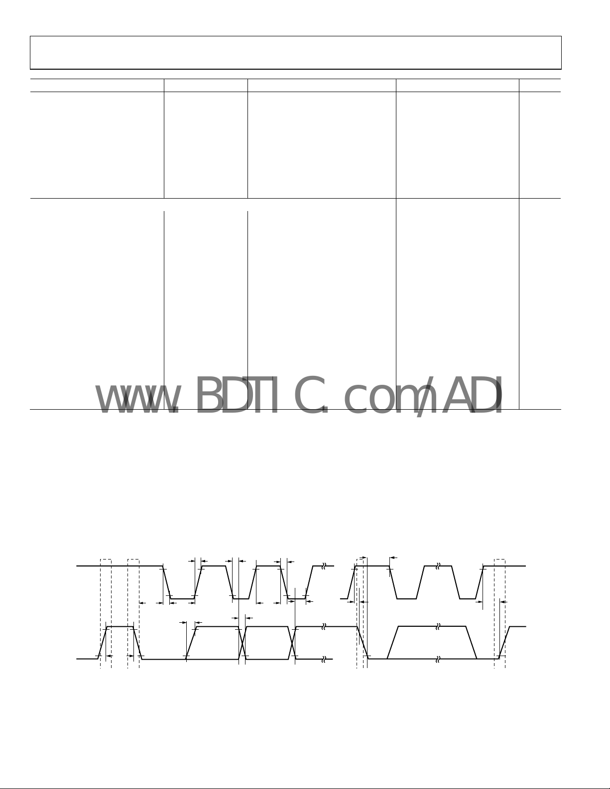
See timing diagram (Figure 3) for location of measured values.
11
Standard I2C mode operation is guaranteed by design.
R
N_WB
SCL
t
1
t
2
t5
t8
t9
t10
= 20 kΩ, f = 1 kHz
WB
6, 10 , 11
After this period, the first clock pulse
is generated
with VW2 = 5 V p-p @ f =
W1
0
1.3
0.6
1.3
0.6
0.6
0
100
0.6
−62
18
dB
nV/√Hz
400 kHz
μs
μs
μs
μs
μs
0.9 μs
ns
300 ns
300 ns
μs
t
t
8
t
t
6
9
2
SCL
t
DA
t
1
PS S
t
2
3
t
9
t
8
t
4
Figure 3. Detailed Timing Diagram
Rev. B | Page 4 of 28
t
7
t
5
t
10
02929-042
P
AD5280/AD5282
www.BDTIC.com/ADI
ABSOLUTE MAXIMUM RATINGS
TA = 25°C, unless otherwise noted.
Table 2.
Parameter Rating
VDD to GND −0.3 V to +16.5 V
VSS to GND 0 V to −7 V
VDD to VSS 16.5 V
VA, VB, VW to GND VSS to V
AX to BX, AX to WX, BX to W
Intermittent
Continuous ±5 mA
V
to GND 0 V to 7 V
LOGI C
Output Voltage to GND 0 V to 7 V
Operating Temperature Range −40°C to +85°C
Maximum Junction Temperature (T
Storage Temperature Range −65°C to +150°C
Reflow Soldering
Peak Temperature 260°C
Time at Peak Temperature 20 sec to 40 sec
3
Maximum terminal current is bound by the maximum current handling of
the switches, maximum power dissipation of the package, and maximum
applied voltage across any two of the A, B, and W terminals at a given
resistance.
3
X
) 150°C
JMAX
±20 mA
DD
Stresses above those listed under Absolute Maximum Ratings
may cause permanent damage to the device. This is a stress
rating only; functional operation of the device at these or any
other conditions above those indicated in the operational
section of this specification is not implied. Exposure to absolute
maximum rating conditions for extended periods may affect
device reliability.
THERMAL RESISTANCE
θJA is specified for the worst-case conditions, that is, a device
soldered in a circuit board for surface-mount packages. Package
power dissipation = (T
JMAX
− TA)/ θ
JA .
Table 3. Thermal Resistance
Package Type θJA Unit
TSSOP-14 206 °C/W
TSSOP-16 150 °C/W
ESD CAUTION
Rev. B | Page 5 of 28
AD5280/AD5282
www.BDTIC.com/ADI
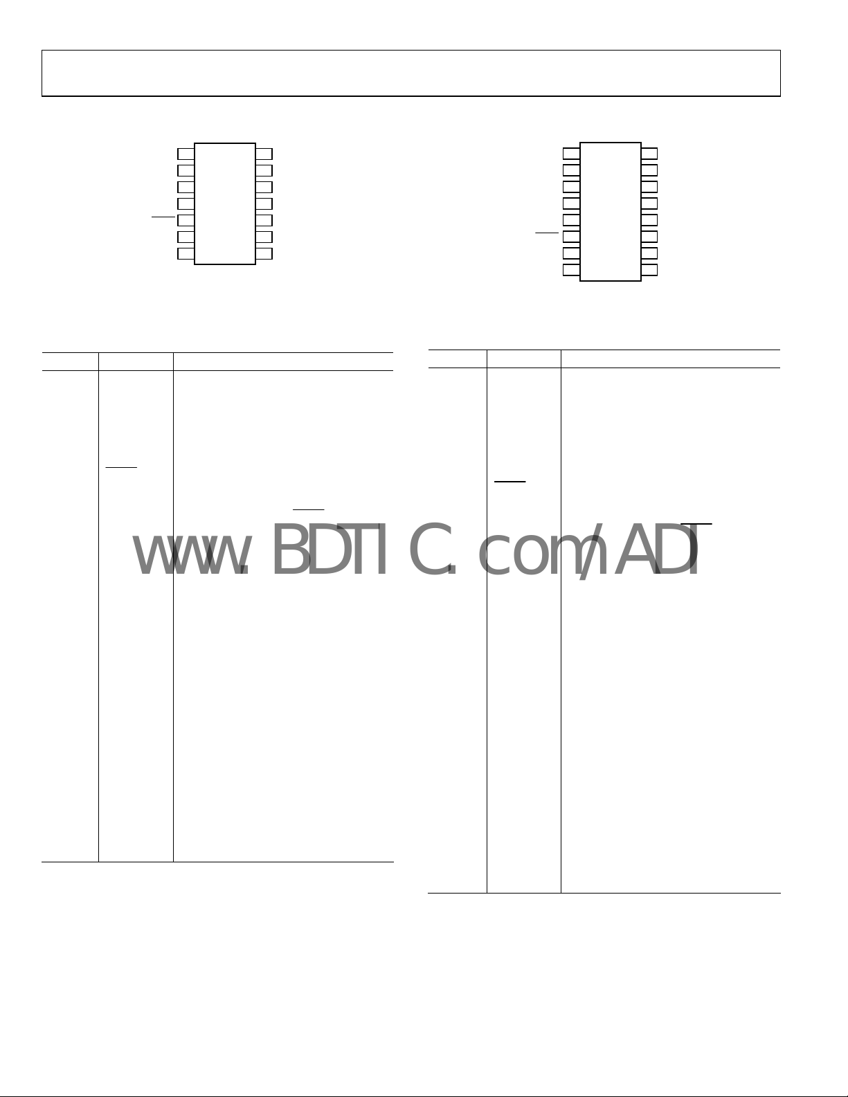
PIN CONFIGURATIONS AND FUNCTION DESCRIPTIONS
V
SHDN
SCL
SDA
1
A
2
W
3
B
AD5280
TOP VIEW
4
DD
5
6
7
14
O
1
13
V
L
12
O
2
11
V
SS
10
GND
9
AD1
8
AD0
Figure 4. AD5280 Pin Configuration
Table 4. AD5280 Pin Function Descriptions
Pin No. Mnemonic Description
1 A Resistor Terminal A.
2 W Wiper Terminal W.
3 B Resistor Terminal B.
4 VDD
Positive Power Supply. Specified for
operation from 5 V to 15 V (sum of |V
+ |V
| ≤ 15 V).
SS
5
Active Low, Asynchronous Connection
SHDN
of Wiper W to Terminal B and Open
Circuit of Terminal A. RDAC register
contents unchanged. SHDN should tie
to V
if not used. Can also be used as a
L
programmable preset in power-up.
6 SCL Serial Clock Input.
7 SDA Serial Data Input/Output.
8 AD0
Programmable Address Bit 0 for
ultiple Package Decoding. Bit AD0
M
and Bit AD1 provide four possible
addresses.
9 AD1
Programmable Address Bit 1 for
ultiple Package Decoding. Bit AD0
M
and Bit AD1 provide four possible
addresses.
10 GND Common Ground.
11 VSS
Negative Power Supply. Specified for
operation from 0 V to −5 V (sum of |V
+ |V
| ≤ 15 V).
SS
12 O2 Logic Output Terminal O2.
13 VL
Logic Supply Voltage. Needs to be less
than or equal to V
and at the same
DD
voltage as the digital logic controlling
the AD5280.
14 O1 Logic Output Terminal O1.
1
O
1
2
A
1
3
W
1
AD5282
4
B
1
TOP VIEW
5
V
DD
6
SHDN
7
02929-002
SCL
SDA
8
16
A
2
15
W
2
14
B
2
13
V
L
12
V
SS
11
GND
10
AD1
9
AD0
02929-003
Figure 5. AD5282 Pin Configuration
Table 5. AD5282 Pin Function Descriptions
Pin No. Mnemonic Description
1 O1 Logic Output Terminal O1.
2 A1 Resistor Terminal A1.
3 W1 Wiper Terminal W1.
4 B1 Resistor Terminal B1.
|
DD
5 VDD
6
SHDN
Positive Power Supply. Specified for
operation from 5 V to 15 V (sum of |V
+ |V
| ≤ 15 V).
SS
DD
Active Low, Asynchronous Connection
|
of Wiper W to Terminal B and Open
Circuit of Terminal A. RDAC register
contents unchanged. SHDN should tie
to V
if not used. Can be also used as a
L
programmable preset in power-up.
7 SCL Serial Clock Input.
8 SDA
9 AD0
Serial Data Input/Output.
Programmable Address Bit 0 for
Multiple Package Decoding. Bit AD0
and Bit AD1 provide four possible
addresses.
10 AD1
Programmable Address Bit 1 for
Multiple Package Decoding. Bit AD0
and Bit AD1 provide four possible
addresses.
11 GND
|
DD
12 V
13 V
SS
L
Common Ground.
Negative Power Supply. Specified for
operation from 0 V to −5 V (sum of |V
+ |V
| ≤ 15 V).
SS
Logic Supply Voltage. Needs to be less
than or equal to V
and at the same
DD
|
DD
voltage as the digital logic controlling
the AD5282.
14 B
Resistor Terminal B2.
2
15 W2 Wiper Terminal W2.
16 A2 Resistor Terminal A2.
Rev. B | Page 6 of 28
AD5280/AD5282
www.BDTIC.com/ADI
TYPICAL PERFORMANCE CHARACTERISTICS
1.0
0.8
0.6
0.4
0.2
0
–0.2
–0.4
RHEOSTAT MO DE R-INL (LSB)
–0.6
–0.8
–1.0
0 32 96 160 22464 128 192 256
+5V
±5V
+15V
CODE (Decimal)
R
T
Figure 6. R-INL vs. Code vs. Supply Voltages
0.5
0.4
0.3
0.2
0.1
0
–0.1
–0.2
–0.3
RHEOSTAT MODE R-DNL (LSB)
–0.8
–0.5
0 32 96 160 22464 128 192 256
±5V +15V
+5V
CODE (Decimal)
R
T
Figure 7. R-DNL vs. Code vs. Supply Voltages
1.0
R
DD/VSS
AB
= ±5 V
0.8
0.6
0.4
0.2
0
–0.2
–0.4
–0.6
POTENTI OMETER MO DE INL (LSB)
–0.8
–1.0
TA = +85°C
TA = –40°C
TA = +25°C
0 32 96 160 22464 128 192 256
CODE (Decimal)
Figure 8. INL vs. Code, V
AB
= 25°C
A
AB
= 25°C
A
= 20k
= 20k
02929-004
= 20k
02929-005
02929-006
0.5
0.4
0.3
0.2
TA = –40°C TA = +85°C
0.1
0
–0.1
–0.2
–0.3
POTENTI OMETER MO DE DNL (LSB)
–0.4
–0.5
0 32 96 160 22464 128 192 256
CODE (Decimal)
Figure 9. DNL vs. Code, V
1.0
0.8
0.6
0.4
0.2
0
–0.2
–0.4
–0.6
POTENTI OMETER MO DE INL (LSB)
–0.8
–1.0
0 32 96 160 22464 128 192 256
±5V
+5V
CODE (Decimal)
DD/VSS
RAB = 20k
= ±5 V
RAB = 20k
T
+15V
Figure 10. INL vs. Code vs. Supply Voltages
0.5
+15V
RAB = 20k
T
0.4
0.3
0.2
0.1
0
–0.1
–0.2
–0.3
POTENTI OMETER MO DE INL (LSB)
–0.4
–0.5
±5V
0 32 96 160 22464 128 192 256
+5V
CODE (Decimal)
Figure 11. DNL vs. Code vs. Supply Voltages
T
= 25°C
A
= 25°C
A
= +25°C
A
02929-007
02929-008
02929-009
Rev. B | Page 7 of 28
AD5280/AD5282
www.BDTIC.com/ADI
1.0
AVG +3
0.5
0
INL (LSB)
–0.5
–1.0
0 5 10 15 20
2.0
1.5
1.0
0.5
0
R-INL (LSB)
–0.5
–1.0
–1.5
AVG
AVG –3
Figure 12. INL Over Supply Voltage
AVG +3
AVG
AVG –3
|VDD– VSS| (V)
RAB = 20k
T
= 25°C
A
RAB = 20k
T
= 25°C
A
2.0
1.8
1.6
1.4
1.2
1.0
0.8
0.6
ZERO-SCALE ERROR (LSB)
0.4
0.2
02929-010
0
–40 0–20 20 40 60 80 100
VDD/VSS= +5V/0V
VDD/VSS= ±5V
VDD/VSS= +15V/0V
TEMPERATURE (°C)
RAB = 20k
02929-013
Figure 15. Zero-Scale Error
1000
100
|SS@VDD/VSS= +15V/0V
SUPPLY CURRENT (nA)
10
SS
/I
DD
I
|SS@VDD/VSS= ±5V
RAB = 20k V
|DD@VDD/VSS= ±5V
LOGIC
V
IH
V
IL
= +5V
= 0V
= +5V
–2.0
0 5 10 15 20
|VDD– VSS| (V)
Figure 13. R-INL Over Supply Voltage
0
–0.2
–0.4
–0.6
–0.8
–1.0
–1.2
–1.4
FULL-SCALE ERROR (LSB)
–1.6
–1.8
–2.0
–40 0–20 20 40 60 80 100
VDD/VSS= +15V/0V
VDD/VSS= ±5V
VDD/VSS= +5V/0V
TEMPERATURE (°C)
RAB = 20k
Figure 14. Full-Scale Error
02929-011
1
–40 –7 26 59 85
TEMPERATURE (°C)
02929-014
Figure 16. Supply Current vs. Temperature
26.0
25.5
25.0
(µA)
24.5
LOGIC
I
24.0
23.5
02929-012
23.0
–40 –7 26 59 85
Figure 17. V
TEMPERATURE ( °C)
Supply Current vs. Temperature
LOGIC
RAB = 20k
VDD/VSS= +15V/0V
VDD/VSS= ±5V
02929-015
Rev. B | Page 8 of 28
AD5280/AD5282
A
www.BDTIC.com/ADI
1000
VDD/VSS= 5V/0V
V
LOGIC
(µA)
100
LOGIC
I
VDD/VSS= 5V/0V
V
= 3V
LOGIC
10
01234
Figure 18. V
700
600
500
400
300
200
T MODE TEMPCO (ppm/°C)
100
0
RHEOST
–100
–200
0 32 64 19296 128 224 256
Supply Current vs. Digital Input Voltage
LOGIC
20k
50k
200k
Figure 19. Rheostat Mode Tempco ΔR
120
100
80
60
40
20
0
–20
POTENTI OMETER MO DE TEMPCO (ppm/° C)
–40
0 32 64 19296 128 224 256
20k
50k
200k
Figure 20. Potentiometer Mode Tempco ΔV
(V)
V
IH
CODE (Decimal)
WB
CODE (Decimal)
= ±5 V
V
DD/VSS
/ΔT vs. Code, VDD/VSS = ±5 V
WB
RAB = 20k
T
= 25°C
A
= 5V
TA = 25°C
TA = 25°C
/ΔT vs. Code,
02929-016
5
02929-017
02929-018
0
–6
–12
–18
–24
–30
GAIN (dB)
–36
–42
–48
–54
–60
0 10k 100k 1M
80H
40H
20H
10H
08H
04H
02H
01H
FREQUENCY (Hz)
TA = 25°C
V
V
Figure 21. Gain vs. Frequency vs. Code, R
0
–6
–12
–18
–24
–30
GAIN (dB)
–36
–42
–48
–54
–60
0 10k 100k 1M
80H
40H
20H
10H
08H
04H
02H
01H
FREQUENCY (Hz)
TA = 25°C
V
V
Figure 22. Gain vs. Frequency vs. Code, R
0
–6
–12
–18
–24
–30
GAIN (dB)
–36
–42
–48
–54
–60
0 10k 100k 1M
80H
40H
20H
10H
08H
04H
02H
01H
FREQUENCY (Hz)
TA = 25°C
V
V
Figure 23. Gain vs. Frequency vs. Code, R
= 50mV rms
A
= ±5V
DD/VSS
= 20 kΩ
AB
= 50mV rms
A
= ±5
DD/VSS
= 50 kΩ
AB
= 50mV rms
A
= ±5V
DD/VSS
= 200 kΩ
AB
02929-019
02929-020
02929-021
Rev. B | Page 9 of 28
AD5280/AD5282
A
(
www.BDTIC.com/ADI
0
–6
–12
–18
–24
–30
GAIN (dB)
–36
–42
–48
–54
–60
0 10k 100k 1M
Figure 24. −3 dB
R = 50k
150kHz
R = 200k
35kHz
FREQUENCY (Hz)
Bandwidth
R = 20k
310kHz
TA = 25°C
V
DD/VSS
V
= 50mV rms
A
= ±5V
80
60
40
PSRR (dB)
20
02929-022
0
100 1000 10k 100k 1M
+PSRR @ VDD/VSS = ±5V
DC ±10% p-p AC
CODE = 80H, VA = VDD, VB = 0V
–PSRR @ VDD/VSS = ±5V
DC ±10% p-p AC
FREQUENCY ( MHz)
02929-025
Figure 27. PSRR v s. Frequency
TA = 25°C
V
DD/VSS
–6dB
TNESS (0.1dB/DIV)
R = 200k
NOMINALIZED GAIN FL
100 1k 10k 100k
FREQUENCY (Hz)
R = 50k
Figure 25. Normalized Gain Flatness vs. Frequency
500
400
300
A)
m
LOGIC
200
I
100
0
10k 100k 1M 10M
Figure 26. V
FREQUENCY (Hz)
Supply Current vs. Frequency
LOGIC
TA = 25°C
V
DD/VSS
CODE = 55
CODE = 55
= ±5V
R = 20k
= ±5V
H
A2 1.2V 852.0µ s
02929-023
2.04µs
02929-026
Figure 28. Midscale Glitch Energy Code 0x80 to 0x7F
T
+5V
1
2
H
02929-024
CH1 5.00V CH2 5.00V M100ns A CH1 0V
V
CS
W
–5V
02929-027
Figure 29. Large Signal Settling Time
Rev. B | Page 10 of 28

AD5280/AD5282
A
C
www.BDTIC.com/ADI
40
30
Y (MHz)
20
FREQUEN
10
CODES SET TO
MIDSCALE
3 LOTS
SAMPLE SIZE = 135
A2 1.0V 33.41µs
1.50µs
Figure 30. Digital Feedthrough vs. Time
100
10
(mA)
WB_MAX
1.0
L |
0.1
THEORETIC
0.01
0 32 64 19296 128 224 256
CODE (Decimal)
Figure 31. I
WB_MAX
VA = VB = OPEN
T
RAB = 20k
RAB = 50k
RAB = 200k
vs. Code
= 25°C
A
02929-028
0
–0.5
–0.4
–0.3
–0.2
–0.45
–0.35
LONG TERM CHANNEL-TO-CHANNE L RAB MATCH (%)
–0.25
–0.1
–0.15
–0.05
0
0.05
02929-030
0.2
0.1
0.15
Figure 32. Channel-to-Channel Resistance Matching (AD5282)
02929-029
Rev. B | Page 11 of 28
AD5280/AD5282
VDD/R
V
%
A
T
T
V
A
V
www.BDTIC.com/ADI
TEST CIRCUITS
Figure 33 to Figure 43 define the test conditions used in the product specification table.
DUT
V+ = V
DD
V
RW = [V
N
V
MS
I
W
MS
NOMINAL
MS1–VMS2
02929-031
02929-032
OFFSET
]/I
W
02929-033
1LSB = V+/2
A
V+
W
B
Figure 33. Potentiometer Divider Nonlinearity Error (INL, DNL)
NO CONNECT
DUT
A
W
B
Figure 34. Resistor Position Nonlinearity Error
stat Operation; R-INL, R-DNL)
(Rheo
DUT
V
MS2
A
B
IW =
V
W
W
V
MS1
OFFSET
GND
OFFSET
GND
GND
B
DUT
V
IN
5V
W
OP279
OFFSET
BIAS
Figure 37. Inverting Gain
5
OP279
V
IN
DUT
OFFSET
BIAS
W
BA
Figure 38. Noninverting Gain
+15V
V
DUT
IN
2.5V
W
AD8610
B
–15V
V
OU
02929-035
V
OU
02929-036
V
OUT
02929-037
Figure 35. Wiper Resistance
V
A
V
DD
V+
A
B
+ = VDD±10
PSRR (dB) = 20 LOG
PSS (%/%) =
W
V
MS
VMS%
V
DD
( )
%
Figure 36. Power Supply Sensitivity (PSS, PSSR)
V
V
MS
DD
02929-034
Figure 39. Gain vs. Frequency
0.1
=
R
SW
I
DUT
W
B
V
SW
I
SW
TO V
SS
0.1V
DD
02929-038
Figure 40. Incremental On Resistance
Rev. B | Page 12 of 28
AD5280/AD5282
V
www.BDTIC.com/ADI
NC
NC = NO CONNECT
V
DUT
V
GND
NC
A
W
B
DD
SS
I
CM
V
Figure 41. Common-Mode Leakage Current
N/C
IN
CM
02929-039
CTA = 20 LOG [V
Figure 43. Analog Crosstalk (AD5282 Only)
A
1
RDAC
W
1
V
DD
A
2
V
SS
RDAC
OUT/VIN
2
W
2
V
OUT
B
2
02929-041
]
1
B
1
I
LOGIC
DIGITAL INPUT
VOLTAGE
2929-040
SCL
SCA
Figure 42. V
V
LOGIC
Current vs. Digital Input Voltage
LOGIC
Rev. B | Page 13 of 28

AD5280/AD5282
−
www.BDTIC.com/ADI
THEORY OF OPERATION
The AD5280/AD5282 are single-channel and dual-channel,
256-position, digitally controlled variable resistors (VRs). To
program the VR settings, see the
arts have an internal power-on preset that places the wiper at
p
midscale during power-on, which simplifies the fault condition
recovery at power-up. Operation of the power-on preset function
also depends on the state of the V
SHDN
D7
D6
D5
D4
D3
D2
D1
D0
RDAC
LATCH
AND
DECODER
Figure 44. AD5280/AD5282 Equivalent RDAC Circuit
RHEOSTAT OPERATION
The nominal resistance of the RDAC between Terminal A and
Terminal B is available in 20 kΩ, 50 kΩ, and 200 kΩ. The final
two or three digits of the part number determine the nominal
resistance value, for example, 20 kΩ = 20, 50 kΩ = 50, and
200 kΩ = 200. The nominal resistance (R
256 contact points accessed by the wiper terminal, plus the B
terminal contact. The eight-bit data in the RDAC latch is
decoded to select one of the 256 possible settings. Assuming
that a 20 kΩ part is used, the wiper’s first connection starts at
the B terminal for data 0x00. Because there is a 60 Ω wiper
contact resistance, such a connection yields a minimum of 60 Ω
resistance between Terminal W and Terminal B.
The second connection is the first tap point that corresponds to
138 Ω (R
third connection is the next tap point representing 216 Ω (78 ×
2 + 60) for data 0x02, and so on. Each LSB data value increase
moves the wiper up the resistor ladder until the last tap point is
reached at 19,982 Ω (R
simplified diagram of the equivalent RDAC circuit where the
last resistor string is not accessed; therefore, there is 1 LSB less
of the nominal resistance at full scale in addition to the wiper
resistance.
= RAB/256 + RW = 78 Ω + 60 Ω) for data 0x01. The
WB
AB
Digital Interface section. Both
pin.
L
A
X
W
X
B
B
X
02929-045
) of the VR has
AB
R
R
R
R
S
S
S
S
SW
A
0xFF
0x01 SW
0x00
– 1 LSB + RW). Figure 46 shows a
The general equation determining the digitally programmed
utput resistance between W and B is
o
WB
()
DR +×=
D
256
AB
(1)
RR
W
where:
he decimal equivalent of the binary code loaded in the 8-
D is t
bit RDAC register.
R
is the nominal end-to-end resistance.
AB
R
is the wiper resistance contributed by the on resistance of
W
the internal switch.
Note that in the zero-scale condition, a finite wiper resistance
of 60 Ω is present. C
are should be taken to limit the current
flow between W and B in this state to a maximum pulse current
of no more than 20 mA. Otherwise, degradation or possible
destruction of the internal switch contact can occur.
As in the mechanical potentiometer, the resistance of the RDAC
bet
ween Wiper W and Terminal A also produces a digitally
controlled complementary resistance, R
. When these terminals
WA
are used, the B terminal can be opened. Setting the resistance
value for R
starts at a maximum value of resistance and
WA
decreases as the data loaded in the latch increases in value. The
general equation for this operation is
D
256
()
DR +×
=
256
ABWA
The typical distribution of the nominal resistance, R
(2)
RR
W
, from
AB
channel to channel matches within ±1%. Device-to-device
matching is process lot dependent, and it is possible to have a
±30% variation. Because the resistance element is processed in
thin film technology, the change in R
with temperature is very
AB
small (30 ppm/°C).
POTENTIOMETER OPERATION
The digital potentiometer easily generates a voltage divider at
wiper to B and wiper to A to be proportional to the input voltage
at A to B. Unlike the polarity of V
positive, voltage across A to B, W to A, and W to B can be at
either polarity, provided that V
If the effect of the wiper resistance for approximation is ignored,
onnecting the A terminal to 5 V and the B terminal to ground
c
produces an output voltage at the wiper to B starting at 0 V up
to 1 LSB less than 5 V. Each LSB of voltage is equal to the
voltage applied across A to B divided by the 256 positions of the
potentiometer divider. Because the AD5280/AD5282 can be
supplied by dual supplies, the general equation defining the
output voltage at V
with respect to ground for any valid
W
– VSS, which must be
DD
is powered by a negative supply.
SS
Rev. B | Page 14 of 28

AD5280/AD5282
www.BDTIC.com/ADI
input voltage applied to Terminal A and Terminal B is
()
W
D
256
V
+=
A
DV
256
256
D
−
(3)
V
B
For a more accurate calculation that includes the effect of wiper
sistance, V
re
()
W
W
DV +=
can be found as
()
DR
WB
V
A
R
AB
WA
R
()
DR
(4)
V
B
AB
Operation of the digital potentiometer in divider mode results
more accurate operation over temperature. Unlike rheostat
in a
mode, the output voltage is dependent mainly on the ratio of
the internal resistors R
and RWB and not on the absolute
WA
values; therefore, the temperature drift reduces to 5 ppm/°C.
SCL
SDA
START BY
MASTER
191 199
01011
SLAVE ADDRESS BYTE
SCL
SDA
START BY
MASTER
AD1
FRAME 1
1
0 1 0 1 1AD1AD0R/W D7D6D5D4D3D2D1D0 A
Figure 46. Reading Data from a Previously Sel
R/W A/BRSSDO1O2 X X X D7D6D5D4D3D2D1D0AD0
ACK. BY
AD5280/5282
Figure 45. Writing to the RDAC Register
FRAME 1
SLAVE ADDRESS BYTE
ACK. BY
FRAME 2
INSTRUCTION BYTE
91 9
ACK. BY
AD5280/AD5282
DATA BYTE FROM PREVIOUSLY SELECTED
ected RDAC Register in Write Mode
AD5280/AD5282
FRAME 2
FRAME 3
DATA BYT E
NO ACK. BY
MASTER
STOP BY
MASTER
02929-044
ACK. BY
AD5280/5282
STOP BY
MASTER
02929-043
Table 6. Serial Format of Data Accepted from the I2C Bus
S 0 1 0 1 1 AD1 AD0 R/W A A
Slave Address Byte Instruction Byte Data Byte
RS SD O
/B
O2 X X X A D7 D6 D5 D4 D3 D2 D1 D0 A P
1
where:
Abbreviation Equals
S Start condition
P Stop condition
A
X
Acknowledge
Don’t care
AD1, AD0 Package pin programmable address bits
R/W
/B
A
Read enable at high and write enable at low
RDAC subaddress select; 0 = RDAC1 and 1 = RDAC2
RS Midscale reset, active high (only affects selected channel)
SD
Shutdown; same as SHDN
pin operation except inverse logic (only affects selected channel)
O2, O1 Output logic pin latched values; default Logic 0
D7, D6, D5, D4, D3, D2, D1, D0 Data bits
Rev. B | Page 15 of 28

AD5280/AD5282
www.BDTIC.com/ADI
DIGITAL INTERFACE
2-WIRE SERIAL BUS
The AD5280/AD5282 are controlled via an I2C-compatible serial
bus. The RDACs are connected to this bus as slave devices. As
shown in
AD5280/AD52
address and an R/
The 5 MSBs are 01011, and the two bits that follow are determi
device. AD0 and AD1 allow the user to place up to four of the
2
I
protocol operates as follows.
The master initiates data transfer by establishing a start condit
ion, which happens when a high-to-low transition on the SDA
line occurs while SCL is high (see
yte is the slave address byte, which consists of the 7-bit slave
b
address followed by an R/
data is read from or written to the slave device).
The slave whose address corresponds to the transmitted address
r
esponds by pulling the SDA line low during the ninth clock
pulse (this is called the acknowledge bit). At this stage, all other
devices on the bus remain idle while the selected device waits for
data to be written to or read from its serial register. If the R/
is high, the master reads from the slave device. On the other
hand, if the R/
A write operation contains one instruction byte more than a
r
ead operation. Such an instruction byte in write mode follows
the slave address byte. The most significant bit (MSB) of the
instruction byte labeled
low selects RDAC1 and a high selects RDAC2 for the dual
channel AD5282. Set
RS, the second MSB, is the midscale reset. A logic high on this
b
it moves the wiper of a selected channel to the center tap
where RWA = RWB. This feature effectively writes over the
contents of the register and thus, when taken out of reset mode,
the RDAC remains at midscale.
SD, the third MSB, is a shutdown bit. A logic high causes the
elected channel to open circuit at Terminal A while shorting
s
the wiper to Terminal B. This operation yields almost 0 Ω in
rheostat mode or 0 V in potentiometer mode. This SD bit serves
the same function as the
reacts to active low. Also, the
(AD5282) as opposed to the SD bit, which affects only the
channel that is being written to. Note that the shutdown
Figure 45, Figure 46, and Tabl e 6 , the first byte of the
82 is a slave address byte. It has a 7-bit slave
W
bit.
ned by the state of the AD0 pin and the AD1 pin of the
C-compatible devices on one bus. The 2-wire I2C serial bus
Figure 45). The following
W
bit (this bit determines whether
W
W
bit is low, the master writes to the slave device.
A
/B is the RDAC subaddress select. A
A
/B low for the AD5280.
SHDN
pin except that the
SHDN
pin affects both channels
SHDN
pin
bit
operation does not disturb the contents of the register. When
brought out of shutdown, the previous setting is applied to
the RDAC.
The following two bits are O
mable logic outputs that can be used to drive other digital loads,
logic gates, LED drivers, analog switches, and so on. The three
LSBs are don’t care bits (see Figure 45).
After acknowledging the instruction byte, the last byte in write
m
ode is the data byte. Data is transmitted over the serial bus in
sequences of nine clock pulses (eight data bits followed by an
acknowledge bit). The transitions on the SDA line must occur
during the low period of SCL and remain stable during the high
period of SCL (see
In read mode, the data byte follows immediately after the
ack
nowledgment of the slave address byte. Data is transmitted
over the serial bus in sequences of nine clock pulses (a slight
difference from write mode, where there are eight data bits
followed by an acknowledge bit). Similarly, the transitions on
the SDA line must occur during the low period of SCL and
remain stable during the high period of SCL (see
When all data bits have been read or written, a stop condition is
tablished by the master. A stop condition is defined as a low-
es
to-high transition on the SDA line while SCL is high. In write
mode, the master pulls the SDA line high during the tenth clock
pulse to establish a stop condition (see
ode, the master issues a no acknowledge for the ninth clock
m
pulse (that is, the SDA line remains high). The master then
brings the SDA line low before the 10th clock pulse, which goes
high to establish a stop condition (see
A repeated write function gives the user flexibility to update the
DAC output a number of times after addressing and instructing
R
the part only once. During the write cycle, each data byte updates
the RDAC output. For example, after the RDAC has acknowledged its slave address and instruction bytes, the RDAC output
updates after these two bytes. If another byte is written to the
RDAC while it is still addressed to a specific slave device with the
same instruction, this byte updates the output of the selected slave
device. If different instructions are needed, the write mode has to
start with a new slave address, instruction, and data byte again.
Similarly, a repeated read function of RDAC is also allowed.
Figure 45).
and O2. They are extra program-
1
Figure 46).
Figure 45). In read
Figure 46).
Rev. B | Page 16 of 28

AD5280/AD5282
A
V
www.BDTIC.com/ADI
READBACK RDAC VALUE
The AD5280/AD5282 allow the user to read back the RDAC
values in read mode. However, for the dual-channel AD5282,
the channel of interest is the one that is previously selected in
the write mode. When users need to read the RDAC values of
both channels in the AD5282, they can program the first
subaddress in write mode and then change to read mode to read
the first channel value. After that, they can change back to write
mode with the second subaddress and read the second channel
value in read mode again. It is not necessary for users to issue
the Frame 3 data byte in write mode for subsequent readback
operation. Users should refer to
p
rogramming format.
Figure 45 and Figure 46 for the
ADDITIONAL PROGRAMMABLE LOGIC OUTPUT
The AD5280/AD5282 feature additional programmable logic
outputs, O
analog switches, and logic gates. O
logic states of O
and O2, which can be used to drive a digital load,
1
and O2 default to Logic 0. The
1
and O2 can be programmed in Frame 2 under
1
write mode (see Figure 45). These logic outputs have adequate
cu
rrent driving capability to sink/source milliamperes of load.
Users can also activate O
and O2 in three ways without
1
affecting the wiper settings by programming as follows:
• P
erform start, slave address, acknowledge, and instruction
bytes with O
• C
omplete the write cycle with stop, then start, slave address
byte, acknowledge, instruction byte with O
and O2 specified, acknowledge, stop.
1
and O2
1
specified, acknowledge, stop.
ot complete the write cycle by not issuing the stop, then
• N
start, slave address byte, acknowledge, instruction byte
with O
and O2 specified, acknowledge, stop.
1
SELF-CONTAINED SHUTDOWN FUNCTION AND PROGRAMMABLE PRESET
Shutdown can be activated by strobing the
programming the SD bit in the write mode instruction byte.
As shown in Figure 44, when shutdown is asserted, the
AD5280/AD52
82 open SW
to let the A terminal float and
A
short the W terminal to the B terminal. The AD5280/AD5282
consume negligible power during shutdown mode, resuming
the previous setting once the
SHDN
SHDN
pin or
pin is released.
In addition, shutdown can be implemented with the device
dig
ital output as shown in
evice is shut down during power-up, but the user is allowed to
d
Figure 47. In this configuration, the
program the device at any preset levels. When it is done, the
user programs O
high with the valid coding and the device
1
exits from shutdown and responds to the new setting. This selfcontained shutdown function allows absolute shutdown during
power-up, which is crucial in hazardous environments, without
adding extra components. Also, the sleep mode programming
feature during shutdown allows the AD5280/AD5282 to have a
programmable preset at any level, a solution that can be as
effective as using other high cost EEPROM devices. Because of
the extra power drawn on R
chosen for the R
.
PD
Figure 47. Shutdown by Internal Logic Output
, note that a high value should be
PD
O
1
SHDN
R
PD
SDA
SCL
02929-046
MULTIPLE DEVICES ON ONE BUS
Figure 48 shows four AD5282 devices on the same serial bus.
Each has a different slave address because the states of their Pin
AD0 and Pin AD1 are different. This allows each RDAC within
each device to be written to or read from independently. The
master device output bus line drivers are open-drain pulldowns in a fully I
MASTER
2
C-compatible interface.
5
RPR
P
SDA
AD1
AD0
AD5282
5V 5V 5V
SCL SDA
Figure 48. Multiple AD5282 Devices on One Bus
SCL SDA
AD1
AD0
AD5282
SCL SDA
AD1
AD0
AD5282
SD
SCL
SCL
AD1
AD0
AD5282
02929-047
Rev. B | Page 17 of 28

AD5280/AD5282
S
S
V
V
V
V
+5V
V
V
www.BDTIC.com/ADI
LEVEL SHIFT FOR BIDIRECTIONAL INTERFACE
While most old systems can be operated at one voltage, a new
component can be optimized at another. When two systems
operate the same signal at two different voltages, proper level
shifting is needed. For instance, a 3.3 V EEPROM can interface
with a 5 V digital potentiometer. A level-shift scheme is needed
to enable a bidirectional communication so that the setting of
the digital potentiometer can be stored to and retrieved from
the EEPROM.
nd M2 can be any N-channel signal FETs or low threshold
M1 a
FDV301N if V
= 3.3
DD1
DA1
CL1
Figure 49 shows one of the implementations.
falls below 2.5 V.
DD
RPR
3.3V
EEPROM
G
P
SD
M1
G
SD
M2
Figure 49. Level Shift for Different Potential Operation
RPR
P
5V
AD5282
DD2
= 5
SDA2
SCL2
02929-048
DD
V
0
IN
Q3
Q1
0
R2
10k
= –5V
V
SS
Q2
R3
10k
0
V
OUT
0
–5V
02929-050
Figure 51. Level Shift for Bipolar Potential Operation
ESD PROTECTION
All digital inputs are protected with a series input resistor and
parallel Zener ESD structures, as shown in Figure 52. The
rotection applies to digital inputs SDA, SCL, and
p
340
LOGIC
SHDN
.
LEVEL SHIFT FOR NEGATIVE VOLTAGE OPERATION
The digital potentiometer is popular in laser diode driver
applications and certain telecommunications equipment levelsetting applications. These applications are sometimes
operated between ground and a negative supply voltage such
that the systems can be biased at ground to avoid large bypass
capacitors that may significantly impede the ac performance.
Like most digital potentiometers, the AD5280/AD5282 can be
configured with a negative supply (see
–5V
LEVEL SHIFTED
LEVEL SHIFTED
Figure 50. Biased at Negative Voltage
However, the digital inputs must also be level shifted to allow
proper operation because the ground is referenced to the
negative potential.
w transistors and a few resistors. When V
fe
Figure 51 shows one implementation with a
threshold value, Q3 is off, Q1 is off, and Q2 is on. In this state,
V
approaches 0 V. When VIN is above 2 V, Q3 is on, Q1 is on,
OUT
and Q2 is turned off. In this state, V
Be aware that proper time shifting is also needed for successful
communication with the device.
Figure 50).
V
DD
V
SS
GND
SDA
SCL
is pulled down to VSS.
OUT
02929-049
is below the Q3
IN
V
SS
02929-051
Figure 52. ESD Protection of Digital Pins
TERMINAL VOLTAGE OPERATING RANGE
The AD5280/AD5282 positive VDD and negative VSS power
supply defines the boundary conditions for proper 3-terminal
digital potentiometer operation. Supply signals present on
Re s is t or Te r mi na l A, R es i sto r Ter mi n al B , an d Wip e r Te r mi n al
W that exceed V
or VSS are clamped by the internal forward-
DD
biased diodes (see Figure 53).
DD
A
W
B
V
SS
02929-053
Figure 53. Maximum Terminal Voltages Set by V
and V
DD
SS
POWER-UP SEQUENCE
Because there are ESD protection diodes that limit the voltage
compliance at Terminal A, Terminal B, and Terminal W (see
Figure 53), it is important to power V
voltage to the A, B, and W terminals. Otherwise, the diode is
forward biased such that V
is unintentionally powered,
DD/VSS
which may affect the rest of the user’s circuit. The ideal powerup sequence is the following: GND, V
V
A/VB/VW
. The order of powering VA/VB/VW and digital inputs
is not important as long as they are powered after V
before applying any
DD/VSS
, VSS, digital inputs, and
DD
DD/VSS
.
Rev. B | Page 18 of 28

AD5280/AD5282
www.BDTIC.com/ADI
LAYOUT AND POWER SUPPLY BYPASSING
It is a good practice to design a layout with compact, minimum
lead lengths. The leads to the input should be as direct as possible
with a minimum conductor length. Ground paths should have
low resistance and low inductance.
Similarly, it is also a good practice to bypass the power supplies
wi
th quality capacitors for optimum stability. Supply leads to
the device should be bypassed with 0.01 μF to 0.1 μF disc or
chip ceramic capacitors. Low ESR 1 μF to 10 μF tantalum or
electrolytic capacitors should also be applied at the supplies to
minimize any transient disturbance and filter low frequency
ripple (see
be join
minimize digital ground bounce.
Figure 54). Notice that the digital ground should also
ed remotely to the analog ground at one point to
V
DD
+
C3
10µFC10.1µF
+
C4
10µFC20.1µF
V
SS
Figure 54. Power Supply Bypassing
V
DD
AD5280/
AD5282
V
SS
GND
02929-054
Rev. B | Page 19 of 28

AD5280/AD5282
V
A
www.BDTIC.com/ADI
APPLICATIONS INFORMATION
BIPOLAR DC OR AC OPERATION FROM DUAL SUPPLIES
The AD5280/AD5282 can be operated from dual supplies
enabling control of ground-referenced ac signals or bipolar
operation. The ac signal, as high as V
directly across Terminal A to Terminal B with the output taken
from Terminal W. See Figure 55 for a typical circuit connection.
V
DD
MICROCONTROLLER
SCLK SCL
MOSI
GND
SDA
GND
AD5282
V
SS
Figure 55. Bipolar Operation
GAIN CONTROL COMPENSATION
The digital potentiometer is commonly used in gain control
applications such as the noninverting gain amplifier shown in
Figure 56.
200k
B
C2
4.7pF
47k
R
1
C125pF
Figure 56. Typical Noninverting Gain Amplifier
Notice that the RDAC B terminal parasitic capacitance is
connected to the op amp noninverting node. It introduces a 0
for the 1/β
term with 20 dB/decade (dec), whereas a typical op
O
amp GBP has −20 dB/dec characteristics. A large R2 and finite
C1 can cause the 0 frequency to fall well below the crossover
frequency. Thus the rate of closure becomes 40 dB/dec, and the
system has a 0° phase margin at the crossover frequency. The
output may ring or oscillate if the input is a rectangular pulse or
step function. Similarly, it is also likely to ring when switching
between two gain values because this is equivalent to a step
change at the input.
U1
V
I
, can be applied
DD/VSS
A
1
W
1
±2.5V p-p ±5V p-p
B
1
D–80
A
2
W
2
B
2
from Dual Supplies
A
W
V
O
02929-056
+5.0V
H
–5.0V
Depending on the op amp GBP, reducing the feedback resistor
y extend the zero’s frequency far enough to overcome the
ma
problem. A better approach is to include a compensation
capacitor C2 to cancel the effect caused by C1. Optimum
compensation occurs when R1 × C1 = R2 × C2. This is not
an option unless C2 is scaled as if R2 were at its maximum
value. Doing so may overcompensate and compromise the
performance slightly when R2 is set at low values. However, it
avoids the gain peaking, ringing, or oscillation at the worst case.
For critical applications, C2 should be found empirically to suit
the need. In general, C2 in the range of a few picofarads (pF) to
no more than a few tenths of a picofarad is usually adequate for
the compensation.
Similarly, there are W and A terminal capacitances connected to
th
e output (not shown); fortunately, their effect at this node is less
significant and the compensation can be avoided in most cases.
15 V, 8-BIT I2C DAC
DD
02929-055
R
BIAS
DR512
D1
R1
AD5280/AD5282 can be configured as a high voltage DAC, as
high as 15 V. The output is
)(
DV +×=
O
256
V
DD
U1A
V+
AD8512
V–
R2
Figure 57. 8-Bit I
U2
AD5280
200k
B
2
C DAC
RD
2
(5)
)]1(V2.1[
R
1
U1B
AD8512
V
O
02929-057
Rev. B | Page 20 of 28

AD5280/AD5282
V
V
V
O
www.BDTIC.com/ADI
8-BIT BIPOLAR DAC
U
V
V
IN
GND
1
V
TRIM
U
1
OUT
ADR425
+5V
2
B
RR
REF
W
A
+15V
–
OP2177
+
A
1
–15V
Figure 58. 8-Bit Bipolar DAC
Figure 58 shows a low cost, 8-bit, bipolar DAC. It offers the same
number of adjustable steps but not the precision of conventional
DACs. The linearity and temperature coefficients, especially at
low value codes, are skewed by the effects of the digital potentiometer wiper resistance. The output of this circuit is
D
2
256
−= 1
⎞
V
⎟
⎠
(6)
REF
⎛
V ×
⎜
O
⎝
BIPOLAR PROGRAMMABLE GAIN AMPLIFIER
U
2
AD5282
1
AD5282
Figure 59. Bipolar Programmable Gain Amplifier
For applications that require bipolar gain, Figure 59 shows one
implementation similar to the previous circuit. The digital
potentiometer, U
at W
can therefore be programmed between Vi and –KVi at a
2
given U
setting. Configuring A2 in noninverting mode allows
2
linear gain and attenuation. The transfer function is
V
⎛
O
1
⎜
V
⎝
i
where K is t
he ratio of R
W
2
A
B
2
2
A1B
1
W
V
1
DD
+
U
1
R2
+= KK
R1
V+
OP2177
V–
–
A
V
1
S8
, sets the adjustment range. The wiper voltage
1
D2
⎛
⎞
⎜
⎟
256
⎝
⎠
WB1/RWA 1
–kVI
()
1
set by U1.
+15
+
OP2177
–
A
2
–15V
–5V
REF
AD5280
U2–
DD
+
V+
OP2177
V–
–
C1
A
A
V
2
2
S8
⎞
(7)
−+××
⎟
⎠
V
O
2929-058
V
R2
R1
02929-059
As in the previous example, in the simpler and more common
e where K = 1, a single digital AD5280 potentiometer is
cas
used. U
V
is replaced by a matched pair of resistors to apply
1
and −Vi at the ends of the digital potentiometer. The
i
relationship becomes
D2
R2
2
⎛
⎛
V ×
⎜
⎝
⎞
+= 1
1
R1
⎜
⎟
⎝
⎠
256
⎞
(7)
V
−
⎟
iO
⎠
If R2 is large, a compensation capacitor having a few pF may be
eeded to avoid any gain peaking.
n
Tabl e 7 shows the result of adjusting D, with A2 configured as a
ty gain, a gain of 2, and a gain of 10. The result is a bipolar
uni
amplifier with linearly programmable gain and a 256-step
resolution.
Table 7. Result of Bipolar Gain Amplifier
D
R1 = ∞, R2 = 0
R1 = R2 R2 = 9R1
0 −1 −2 −10
64 −0.5 −1 −5
128 0 0 0
192 0.5 1 5
255 0.968 1.937 9.680
PROGRAMMABLE VOLTAGE SOURCE WITH BOOSTED OUTPUT
For applications that require high current adjustments, such as a
laser diode driver or tunable laser, a boosted voltage source can
be considered (see Figure 60).
V
I
5V
A
W
+
U
1
B
V+
A1
–
V–
N
1
SIGNAL
U1= AD5280
= AD8501, AD8605, AD8541
A
1
= FDV301N, 2N7002
N
1
Figure 60. Programmable Booster Voltage Source
In this circuit, the inverting input of the op amp forces the
V
to be equal to the wiper voltage set by the digital potenti-
BIAS
ometer. The load current is then delivered by the supply via the
N-channel FET N1. The N1 power handling must be adequate
to dissipate (V
– VO) × IL power. This circuit can source a
i
maximum of 100 mA with a 5 V supply. A1 needs to be a railto-rail input type. For precision applications, a voltage reference
such as ADR423, ADR292, or AD1584 can be applied at the
put of the digital potentiometer.
in
V
O
R
BIAS
C
C
L
D
I
L
02929-060
Rev. B | Page 21 of 28
AD5280/AD5282
V
A
(
+
(
)
+
×
www.BDTIC.com/ADI
PROGRAMMABLE CURRENT SOURCE
+5
U
1
2
V
IN
3
SLEEP
REF191
GND
4
AD5280
–2.048V TO V
Figure 61. Programmable Current Source
A programmable current source can be implemented with the
circuit shown in Figure 61. REF191 is a unique, low supply
he
adroom and high current handling precision reference that
can deliver 20 mA at 2.048 V. The load current is simply the
voltage across Terminal B to Terminal W of the digital
potentiometer divided by R
L
N
R
2×
S
×
REF
=
I
The circuit is simple, but attention must be paid to two things.
F
irst, dual-supply op amps are ideal because the ground
potential of REF191 can swing from −2.048 V at zero scale to V
at full scale of the potentiometer setting. Although the circuit
works under single supply, the programmable resolution of the
system is reduced.
For applications that demand higher current capabilities, a
fe
w changes to the circuit in Figure 61 produce an adjustable
urrent in the range of hundreds of milliamps. First, the voltage
c
reference needs to be replaced with a high current, low dropout
regulator, such as the ADP3333, and the op amp needs to be
wapped with a high current dual-supply model, such as the
s
AD8532. Depending on the desired range of current, an
ppropriate value for R
a
current flowing to the load, the user must pay attention to the
load impedance so as not to drive the op amp beyond the
positive rail.
0 TO (2.048 + VL)
6
V
OUT
C1
1µF
L
.
S
DV
(8)
must be calculated. Because of the high
S
+5V
V+
OP8510
OP8510
V–
5V
U2
B
W
A
U2
100
R
S
102
V
R
L
L
I
L
02929-061
PROGRAMMABLE BIDIRECTIONAL CURRENT SOURCE
I
R1
150k
+5V
A
D5280
–5V
+15V
W
V+
OP2177
V–
–15V
A
1
R1
150k
Figure 62. Programmable Bidirectional Current Source
For applications that require bidirectional current control or
higher voltage compliance, a Howland current pump can be a
solution (see Figure 62). If the resistors are matched, the load
urrent is
c
)
R2R2
BA
L
In theory, R2
R2
B
can be made as small as needed to achieve the
B
R1
=
I ×
current needed within the A
L
In this circuit, the OP2177 can deliver ±5 mA in either direction,
nd the voltage compliance approaches 15 V. It can be shown
a
(9)
V
W
output current driving capability.
2
that the output impedance is
R2R1R2'R1
=
Z
O
B
A
()
R2R2R1'R2'R1
+−×
B
A
This output impedance can be infinite if Resistor R1' and
Resist
or R2' match precisely with R1 and R2
respectively. On the other hand, it can be negative if the
resistors are not matched. As a result, C1 must be in the range
of 1 pF to 10 pF to prevent the oscillation.
I
R2
15k
C1
+15V
10pF
V+
OP2177
V–
A
2
R2
B
–15V
R2
14.95k
50k
V
L
R
A
L
500k
|
L
02929-062
(10)
+ R2B,
A
Rev. B | Page 22 of 28
AD5280/AD5282
V
RC
RC
R
2
F
www.BDTIC.com/ADI
PROGRAMMABLE LOW-PASS FILTER
In analog-to-digital conversion applications, it is common to
include an antialiasing filter to band-limit the sampling signal.
Dual-channel digital potentiometers can be used to construct
a second-order Sallen key low-pass filter (see Figure 63). The
esign equations are
d
V
O
=
V
i
S
=ω
O
Q
2
ω
O
ω
2
O
S
+
Q
1
R1R2C1C2
11
+= (13)
R2C2R1C1
(11)
2
ω+
O
(12)
Users can first select some convenient values for the capacitors.
o achieve maximally flat bandwidth where Q = 0.707, let C1 be
T
twice the size of C2 and let R1 = R2. As a result, R1 and R2 can be
adjusted to the same settings to achieve the desirable bandwidth.
C1
C
R1
A
I
BR2A
W
R
ADJUSTED TO
SAME SETTING
Figure 63. Sallen Key Lo
B
W
R
C2 C
+2.5V
V+
AD8601
V–
–2.5V
w-Pass Filter
V
O
U
1
02929-063
PROGRAMMABLE OSCILLATOR
In a classic Wien-bridge oscillator (Figure 64), the Wien
network (R, R', C, C') provides positive feedback, while R1
and R2 provide negative feedback. At the resonant frequency, f
the overall phase shift is 0, and the positive feedback causes the
circuit to oscillate. With R = R', C = C', and R2 = R2
), the oscillation frequency is
R
diode
11
ω
where R is e
R
=
qual to R
256
−
256
for
==
oO
WA
D
R
AB
(14)
π
2
such that
(15)
//(R2B +
A
,
O
At resonance, setting the following balances the bridge:
R2
(16)
2=
1
In practice, R2/R1 should be set slightly larger than 2 to ensure
t
hat oscillation can start. On the other hand, the alternate turnon of Diode D1 and Diode D2 ensures that R2/R1 are smaller
than 2 momentarily and, therefore, stabilizes the oscillation.
Once the frequency is set, the oscillation amplitude can be
ned by R2
tu
, ID, and VD are interdependent variables. With proper
V
O
selection of R2
converges. R2
because
B
2
3
, an equilibrium is reached such that VO
B
can be in series with a discrete resistor to
B
(17)
VR2IV +=
DBDO
increase the amplitude, but the total resistance cannot be
too large to prevent saturation of the output.
FREQUENCY
ADJUSTMENT
C
.2n
R1 = R1
D1 = D2 = 1N4148
BA
R
10k
I
= R2B = AD5282
W
A
VN
R1
1k
Figure 64. Programmable Oscillator with Amplitude Control
VP
B
I
C
2.2nF
+2.5V
OP1177
–2.5V
R2
B
10k
A
W
I
R
10k
W
V+
U
1
V–
R2
A
2.1k
AMPLI TUDE
ADJUSTME NT
B
V
O
D1
D2
02929-064
Rev. B | Page 23 of 28

AD5280/AD5282
A
www.BDTIC.com/ADI
RDAC CIRCUIT SIMULATION MODEL
The internal parasitic capacitances and the external capacitive
loads dominate the ac characteristics of the RDACs. Configured
as a potentiometer divider, the −3 dB bandwidth of the AD5280
(20 kΩ resistor) measures 310 kHz at half scale. Figure 24
rovides the Bode plot characteristics of the three available
p
resistor versions: 20 kΩ, 50 kΩ, and 200 kΩ. A parasitic
simulation model is shown in Figure 65. A macro model net list
r the 20 kΩ RDAC is provided.
fo
RDAC
20k
B
MACRO MODEL NET LIST FOR RDAC
.PARAM D=256, RDAC=20E3
*
.SUBCKT DPOT (A,W,B)
*
CA A 0 25E-12
RWA A W {(1-D/256)*RDAC+60}
CW W 0 55E-12
RWB W B {D/256*RDAC+60}
CB B 0 25E-12
*
.ENDS DPOT
C
A
2
5
p
F
C
8
5
Figure 65. RDAC Circuit Simulation Model for RDAC = 20 kΩ
C
A
2
5
p
F
W
p
F
02929-068
Rev. B | Page 24 of 28
AD5280/AD5282
www.BDTIC.com/ADI
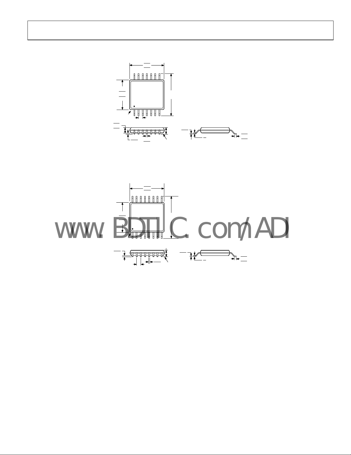
OUTLINE DIMENSIONS
5.10
5.00
4.90
14
4.50
4.40
4.30
PIN 1
1.05
1.00
0.80
0.65
BSC
0.15
0.30
0.05
0.19
COMPLIANT TO JEDEC STANDARDS MO-153-AB-1
Figure 66. 14-Lead Thin Shrink S
Dimensions shown in millimeters
5.10
5.00
4.90
16
4.50
4.40
4.30
PIN 1
0.15
0.05
0.65
BSC
COPLANARITY
0.30
0.19
0.10
COMPLIANT TO JEDEC STANDARDS MO-153-AB
Figure 67. 16-Lead Thin Shrink S
Dimensions shown in millimeters
8
6.40
BSC
71
1.20
MAX
SEATING
PLANE
9
6.40
BSC
81
1.20
MAX
SEATING
PLANE
0.20
0.09
COPLANARITY
0.10
8°
0°
mall Outline Package (TSSOP)
(RU-14)
0.20
0.09
8°
0°
mall Outline Package (TSSOP)
(RU-16)
0.75
0.60
0.45
0.75
0.60
0.45
Rev. B | Page 25 of 28

AD5280/AD5282
www.BDTIC.com/ADI
ORDERING GUIDE
1
Model
AD5280BRU20 1 20 −40°C to +85°C 14-Lead TSSOP RU-14 96
AD5280BRU20-REEL7 1 20 −40°C to +85°C 14-Lead TSSOP RU-14 1,000
AD5280BRU50 1 50 −40°C to +85°C 14-Lead TSSOP RU-14 96
AD5280BRU50-REEL7 1 50 −40°C to +85°C 14-Lead TSSOP RU-14 1,000
AD5280BRU200 1 200 −40°C to +85°C 14-Lead TSSOP RU-14 96
AD5280BRU200-REEL7 1 200 −40°C to +85°C 14-Lead TSSOP RU-14 1,000
AD5280BRUZ20
AD5280BRUZ20-REEL721 20 −40°C to +85°C 14-Lead TSSOP RU-14 1,000
AD5280BRUZ50
AD5280BRUZ50-REEL721 50 −40°C to +85°C 14-Lead TSSOP RU-14 1,000
AD5280BRUZ200
AD5280BRUZ200-R7
AD5282BRU20 2 20 −40°C to +85°C 16-Lead TSSOP RU-16 96
AD5282BRU20-REEL7 2 20 −40°C to +85°C 16-Lead TSSOP RU-16 1,000
AD5282BRU50 2 50 −40°C to +85°C 16-Lead TSSOP RU-16 96
AD5282BRU50-REEL7 2 50 −40°C to +85°C 16-Lead TSSOP RU-16 1,000
AD5282BRU200 2 200 −40°C to +85°C 16-Lead TSSOP RU-16 96
AD5282BRU200-REEL7 2 200 −40°C to +85°C 16-Lead TSSOP RU-16 1,000
AD5282BRUZ20
AD5282BRUZ20-REEL72 2 20 −40°C to +85°C 16-Lead TSSOP RU-16 1,000
AD5282BRUZ50
AD5282BRUZ50-REEL72 2 50 −40°C to +85°C 16-Lead TSSOP RU-16 1,000
AD5282BRUZ200
AD5282BRUZ200-R72 2 200 −40°C to +85°C 16-Lead TSSOP RU-16 1,000
AD5282-EVAL 2 20 Evaluation Board
1
Line 1 contains model number, Line 2 contains ADI logo followed by the end-to-end resistance value, and Line 3 contains date code YYWW.
2
Z = RoHS Compliant Part.
2
2
2
2
2
2
No. of
Channels R
1 20 −40°C to +85°C 14-Lead TSSOP RU-14 96
1 50 −40°C to +85°C 14-Lead TSSOP RU-14 96
1 200 −40°C to +85°C 14-Lead TSSOP RU-14 96
2
1 200 −40°C to +85°C 14-Lead TSSOP RU-14 1,000
2 20 −40°C to +85°C 16-Lead TSSOP RU-16 96
2 50 −40°C to +85°C 16-Lead TSSOP RU-16 96
2 200 −40°C to +85°C 16-Lead TSSOP RU-16 96
(kΩ)
AB
Temperature
R
ange Package Description
Package
Option Ordering Quantity
Rev. B | Page 26 of 28

AD5280/AD5282
www.BDTIC.com/ADI
NOTES
Rev. B | Page 27 of 28

AD5280/AD5282
www.BDTIC.com/ADI
NOTES
©2002–2007 Analog Devices, Inc. All rights reserved. Trademarks and
registered trademarks are the property of their respective owners.
C02929-0-8/07(B)
Rev. B | Page 28 of 28
 Loading...