

1024-/256-Position, 1% Resistor Tolerance Error,
SPI Interface and 50-TP Memory Digital Rheostat
FEATURES
Single-channel, 1024-/256-position resolution
20 kΩ, 50 kΩ, 100 kΩ nominal resistance
Maximum ±1% nominal resistor tolerance error
50-times programmable (50-TP) wiper memory
Rheostat mode temperature coefficient: 5 ppm/°C
2.7 V to 5.5 V single-supply operation
±2.5 V to ±2.75 V dual-supply operation for ac or bipolar
operations
SPI-compatible interface
Wiper setting readback
Power on refreshed from 50-TP memory
Thin LFCSP, 10-lead, 3 mm × 3 mm × 0.8 mm package
Compact MSOP, 10-lead, 3 mm × 4.9 mm × 1.1 mm package
APPLICATIONS
Mechanical rheostat replacements
Op-amp: variable gain control
Instrumentation: gain, offset adjustment
Programmable voltage to current conversions
Programmable filters, delays, time constants
Programmable power supply
Sensor calibration
SCLK
SYNC
DIN
SDO
AD5270/AD5271
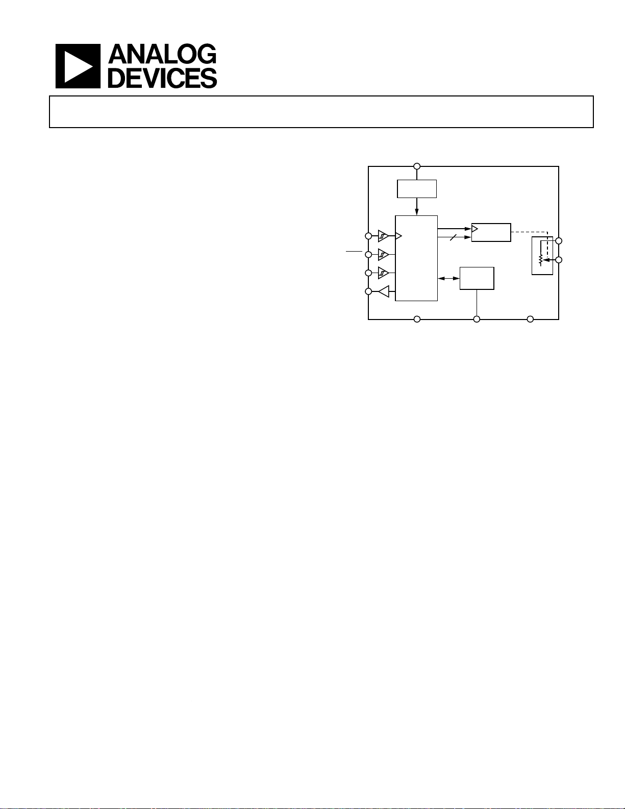
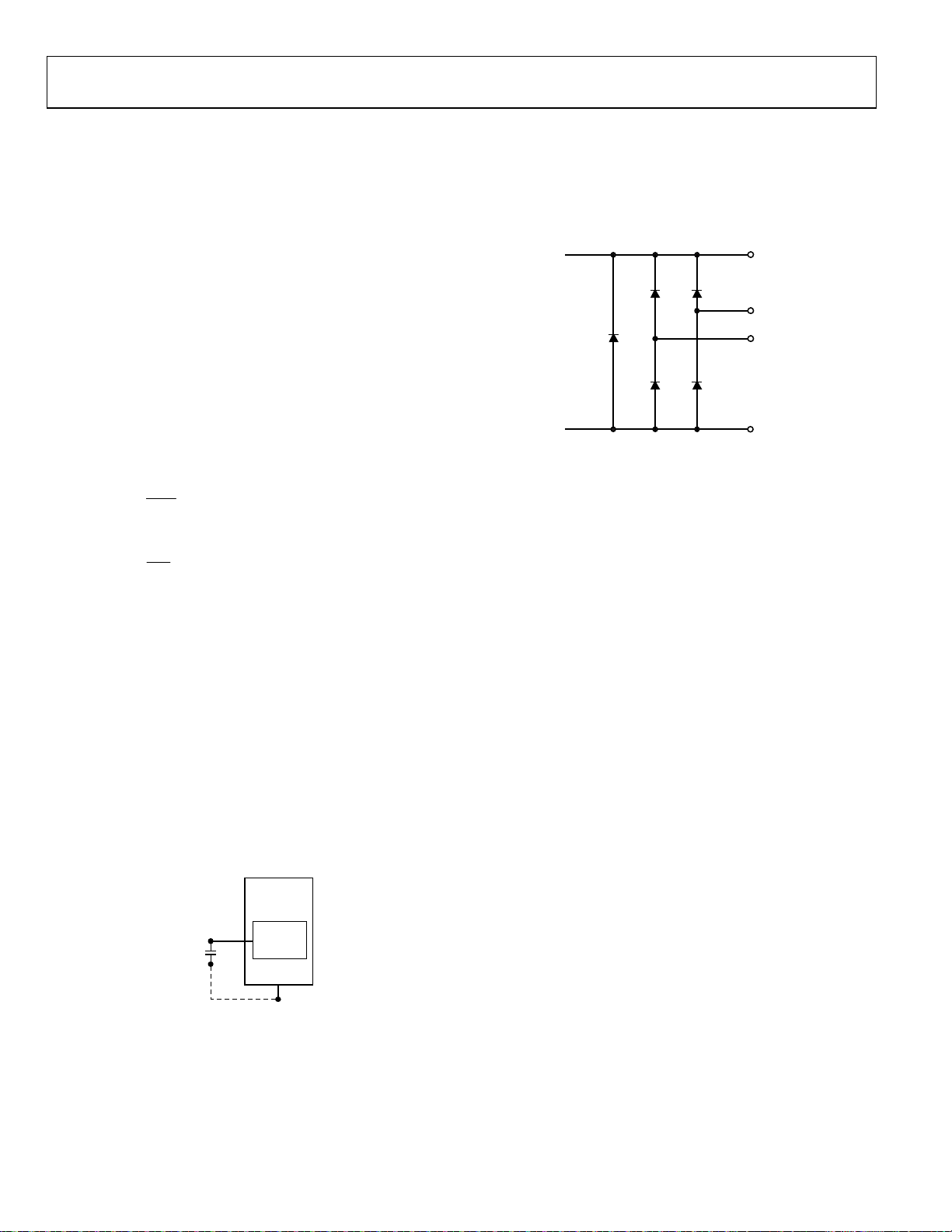
FUNCTIONAL BLOCK DIAGRAM
V
DD
POWER-ON
RESET
SERIAL
INTERFACE
V
SS
AD5270/AD5271
RDAC
REGISTER
10/8
50-TP
MEMORY
BLOCK
EXT_CAP GND
Figure 1.
A
W
08077-001
GENERAL DESCRIPTION
The AD5270/AD52711 are single-channel, 1024-/256-position
digital rheostats that combine industry leading variable resistor
performance with nonvolatile memory (NVM) in a compact
package.
The AD5270/AD5271 ensure less than 1% end-to-end resistor
tolerance error and offer 50-times programmable (50-TP) memory.
The guaranteed industry leading low resistor tolerance error
feature simplifies open-loop applications as well as precision
calibration and tolerance matching applications.
1
Protected by U.S.Patent Number 7688240...;
The AD5270/AD5271 device wiper settings are controllable
through the SPI digital interface. Unlimited adjustments are
allowed before programming the resistance value into the
50-TP memory. The AD5270/AD5271 do not require any
external voltage supply to facilitate fuse blow and there are
50 opportunities for permanent programming. During 50-TP
activation, a permanent blow fuse command freezes the resistance
position (analogous to placing epoxy on a mechanical trimmer).
The AD5270/AD5271 are available in a 3 mm × 3 mm, 10-lead
LFCSP package and in a 10-lead MSOP package. The parts are
guaranteed to operate over the extended industrial temperature
range of −40°C to +125°C.
Rev. E
Information furnished by Analog Devices is believed to be accurate and reliable. However, no
responsibility is assumed by Anal og Devices for its use, nor for any infringements of patents or ot her
rights of third parties that may result from its use. Specifications subject to change without notice. No
license is granted by implication or otherwise under any patent or patent rights of Analog Devices.
Trademarks and registered trademarks are the property of their respective owners.
One Technology Way, P.O. Box 9106, Norwood, MA 02062-9106, U.S.A.
Tel: 781.329.4700 www.analog.com
Fax: 781.461.3113 ©2009–2010 Analog Devices, Inc. All rights reserved.

AD5270/AD5271
TABLE OF CONTENTS
Features.............................................................................................. 1
Applications....................................................................................... 1
Functional Block Diagram .............................................................. 1
General Description ......................................................................... 1
Revision History ............................................................................... 2
Specifications..................................................................................... 3
Electrical Characteristics—AD5270 .......................................... 3
Electrical Characteristics—AD5271 .......................................... 5
Interface Timing Specifications.................................................. 7
Absolute Maximum Ratings............................................................ 9
Thermal Resistance ...................................................................... 9
ESD Caution.................................................................................. 9
Pin Configuration and Function Descriptions........................... 10
Typical Performance Characteristics ........................................... 11
Test Circuits..................................................................................... 17
Theory of Operation ...................................................................... 18
Serial Data Interface................................................................... 18
Shift Register............................................................................... 18
RDAC Register............................................................................ 18
50-TP Memory Block ................................................................ 18
Write Protection ......................................................................... 18
RDAC and 50-TP Read Operation .......................................... 19
Shut-Down Mode....................................................................... 20
Resistor Performance Mode...................................................... 20
Reset ............................................................................................. 20
SDO Pin and Daisy-Chain Operation..................................... 21
RDAC Architecture.................................................................... 21
Programming the Variable Resistor......................................... 22
EXT_CAP Capacitor.................................................................. 22
Terminal Voltage Operating Range ......................................... 22
Power-Up Sequence ................................................................... 22
Outline Dimensions....................................................................... 23
Ordering Guide .......................................................................... 24
REVISION HISTORY
12/10—Rev. D to Rev. E
Changes to SDO Pin Description................................................. 10
Changes to SDO Pin and Daisy-Chain Operation Section....... 21
11/10—Rev. C to Rev. D
Changes to Figure 25...................................................................... 14
9/10—Rev. B to Rev. C
Changes to Figure 3 Caption........................................................... 7
Changes to Figure 4 Caption........................................................... 8
Deleted Daisy-Chain Operation Section, Added SDO Pin and
Daisy-Chain Operation Section ................................................... 21
5/10—Rev. A to Rev. B
Added LFCSP Throughout.............................................................. 1
Changed OTP to 50-TP Throughout............................................. 1
Changes to Product Title, Features, and General Description... 1
Changes to Table 1.............................................................................3
Added Table 3; Renumbered Sequentially .....................................4
Changes to Table 4.............................................................................5
Added Table 6 ....................................................................................6
Changes to Table 8 and Table 9 .......................................................9
Added Figure 6 and changes to Table 10 ..................................... 10
Replaced Typical Performance Characteristics Section ............ 11
Changes to Figure 44...................................................................... 21
Updated Outline Dimensions....................................................... 23
Changes to Ordering Guide.......................................................... 24
3/10—Rev. 0 to Rev. A
Changes to Product Title and General Description.....................1
Changes to Theory of Operation Section...................................14
10/09—Revision 0: Initial Version
Rev. E | Page 2 of 24

AD5270/AD5271
SPECIFICATIONS
ELECTRICAL CHARACTERISTICS—AD5270
VDD = 2.7 V to 5.5 V, VSS = 0 V; VDD = 2.5 V to 2.75 V, VSS = −2.5 V to −2.75 V; −40°C < TA < +125°C, unless otherwise noted.
Table 1.
Parameter Symbol Test Conditions/Comments Min Typ1 Max Unit
DC CHARACTERISTICS—RHEOSTAT MODE
Resolution 10 Bits
Resistor Integral Nonlinearity
R
R
Resistor Differential Nonlinearity2
Nominal Resistor Tolerance
R-Perf Mode4
Normal Mode ±15 %
Resistance Temperature Coefficient
Wiper Resistance Code = zero scale 35 70 Ω
RESISTOR TERMINALS
Terminal Voltage Range
Capacitance5 A
Capacitance5 W
Common-Mode Leakage Current5
DIGITAL INPUTS
Input Logic5
High V
Low V
Input Current IIN ±1 μA
Input Capacitance5
DIGITAL OUTPUT
Output Voltage5
High VOH R
Low VOL R
V
V
Tristate Leakage Current −1 +1 μA
Output Capacitance5
POWER SUPPLIES
Single-Supply Power Range VSS = 0 V 2.7 5.5 V
Dual-Supply Power Range ±2.5 ±2.75 V
Supply Current
Positive IDD 1 μA
Negative ISS −1 μA
50-TP Store Current
Positive I
Negative I
OTP Read Current
5, 9
Positive I
Negative I
5, 8
2, 3
R-INL RAW = 20 kΩ, |VDD − VSS| = 3.0 V to 5.5 V −1 +1 LSB
= 20 kΩ, |VDD − VSS| = 2.7 V to 3.0 V −1 +1.5 LSB
AW
= 50 kΩ, 100 kΩ −1 +1 LSB
AW
−1 +1 LSB
−1 ±0.5 +1 %
V
SS
V
DD
90 pF
5, 7
R-DNL
5, 6
Code = full scale 5 ppm/°C
V
See
Table 2 and Table 3
f = 1 MHz, measured to GND, code =
half scale
f = 1 MHz, measured to GND, code =
40 pF
half scale
V
= VW 50 nA
A
2.0 V
INH
0.8 V
INL
5 pF
C
IN
= 2.2 kΩ to VDD V
PULL_UP
= 2.2 kΩ to VDD
PULL_UP
= 2.7 V to 5.5 V, VSS = 0 V 0.4 V
DD
= 2.5 V to 2.75 V, VSS = −2.5 V to −2.75 V 0.6 V
DD
− 0.1 V
DD
5 pF
DD_OTP_STORE
SS_OTP_STORE
4 mA
−4 mA
DD_OTP_READ
SS_OTP_READ
500 μA
−500 μA
Rev. E | Page 3 of 24
AD5270/AD5271
Parameter Symbol Test Conditions/Comments Min Typ1 Max Unit
Power Dissipation10 V
Power Supply Rejection Ratio5
PSRR ΔV
R
R
R
DYNAMIC CHARACTERISTICS
5, 11
Bandwidth −3 dB, RAW = 10 kΩ, Terminal W,
R
R
R
Total Harmonic Distortion VA = 1 V rms, f = 1 kHz,
R
R
R
Resistor Noise Density Code = half scale, TA = 25°C nV/√Hz
R
R
R
1
Typical specifications represent average readings at 25°C, VDD = 5 V, and VSS = 0 V.
2
Resistor position nonlinearity error (R-INL) is the deviation from an ideal value measured between the maximum resistance and the minimum resistance wiper
positions. R-DNL measures the relative step change from ideal between successive tap positions.
3
The maximum current in each code is defined by IAW = (VDD − 1)/RAW.
4
The terms resistor performance mode and R-Perf mode are used interchangeably. See the Resistor Performance Mode section.
5
Guaranteed by design and not subject to production test.
6
See Figure 25 for more details.
7
Resistor Terminal A and Resistor Terminal W have no limitations on polarity with respect to each other. Dual-supply operation enables ground referenced bipolar
signal adjustment.
8
Different from operating current, the supply current for the fuse program lasts approximately 55 ms.
9
Different from operating current, the supply current for the fuse read lasts approximately 500 ns.
10
P
is calculated from (IDD × VDD) + (ISS × VSS).
DISS
11
All dynamic characteristics use VDD = +2.5 V, VSS = −2.5 V.
= VDD or VIL = GND 5.5 μW
IH
/ΔVSS = ±5 V ± 10% dB
DD
= 20 kΩ −66 −55
AW
= 50 kΩ −75 −67
AW
= 100 kΩ −78 −70
AW
kHz
see
Figure 42
= 20 kΩ 300
AW
= 50 kΩ 120
AW
= 100 kΩ 60
AW
dB
code = half scale
= 20 kΩ −90
AW
= 50 kΩ −88
AW
= 100 kΩ −85
AW
= 20 kΩ 50
AW
= 50 kΩ 25
AW
= 100 kΩ 32
AW
Table 2. AD5270—20 kΩ Resistor Performance Mode Code Range
Resistor Tolerance Per Code |VDD − VSS| = 4.5 V to 5.5 V |VDD − VSS| = 2.7 V to 4.5 V
R-TOLERANCE
1% R-Tolerance From 0x078 to 0x3FF From 0x0BE to 0x3FF
2% R-Tolerance From 0x037 to 0x3FF From 0x055 to 0x3FF
3% R-Tolerance From 0x028 to 0x3FF From 0x037 to 0x3FF
Table 3. AD5270—50 kΩ and 100 kΩ Resistor Performance Mode Code Range
Resistor Tolerance Per Code RAW = 50 kΩ RAW = 100 kΩ
R-TOLERANCE
1% R-Tolerance From 0x078 to 0x3FF From 0x04B to 0x3FF
2% R-Tolerance From 0x055 to 0x3FF From 0x032 to 0x3FF
3% R-Tolerance From 0x032 to 0x3FF From 0x019 to 0x3FF
Rev. E | Page 4 of 24

AD5270/AD5271
ELECTRICAL CHARACTERISTICS—AD5271
VDD = 2.7 V to 5.5 V, VSS = 0 V; VDD = 2.5 V to 2.75 V, VSS = −2.5 V to −2.75 V; −40°C < TA < +125°C, unless otherwise noted.
Table 4.
Parameter Symbol Test Conditions/Comments Min Typ1 Max Unit
DC CHARACTERISTICS—RHEOSTAT MODE
Resolution 8 Bits
Resistor Integral Nonlinearity
Resistor Differential Nonlinearity2 R-DNL
Nominal Resistor Tolerance
R-Perf Mode4 See Table 5 and Table 6 −1 ±0.5 +1 %
Normal Mode ±15 %
Resistance Temperature Coefficient
Wiper Resistance Code = zero scale 35 70 Ω
RESISTOR TERMINALS
Terminal Voltage Range
Capacitance5 A
Capacitance5 W
Common-Mode Leakage Current5 V
DIGITAL INPUTS
Input Logic5
High V
Low5 V
Input Current IIN ±1 μA
Input Capacitance5 C
DIGITAL OUTPUT
Output Voltage5
High VOH R
Low VOL R
V
V
Tristate Leakage Current −1 +1 μA
Output Capacitance5 5 pF
POWER SUPPLIES
Single-Supply Power Range VSS = 0 V 2.7 5.5 V
Dual-Supply Power Range ±2.5 ±2.75 V
Supply Current
Positive IDD 1 μA
Negative ISS −1 μA
50-TP Store Current
Positive I
Negative I
OTP Read Current
5, 9
Positive I
Negative I
Power Dissipation10 V
Power Supply Rejection Ratio5 PSRR ΔVDD/ΔVSS = ±5 V ± 10% dB
R
R
R
2, 3
R-INL −1 +1 LSB
5, 6
Code = full scale 5 ppm/°C
5, 7
V
f = 1 MHz, measured to GND, code =
−1 +1 LSB
V
SS
V
DD
90 pF
half scale
f = 1 MHz, measured to GND, code =
40 pF
half scale
= VW 50 nA
A
2.0 V
INH
0.8 V
INL
5 pF
IN
= 2.2 kΩ to VDD V
PULL_UP
= 2.2 kΩ to VDD
PULL_UP
= 2.7 V to 5.5 V, VSS = 0 V 0.4 V
DD
= 2.5 V to 2.75 V, VSS = −2.5 V to −2.75 V 0.6 V
DD
5, 8
DD_OTP_STORE
SS_OTP_STORE
4 mA
−4 mA
− 0.1 V
DD
DD_OTP_READ
SS_OTP_READ
500 μA
−500 μA
= VDD or VIL = GND 5.5 μW
IH
= 20 kΩ −66 −55
AW
= 50 kΩ −75 −67
AW
= 100 kΩ −78 −70
AW
Rev. E | Page 5 of 24
AD5270/AD5271
Parameter Symbol Test Conditions/Comments Min Typ1 Max Unit
DYNAMIC CHARACTERISTICS
Bandwidth −3 dB, RAW = 10 kΩ, Terminal W, see Figure 42 kHz
R
R
R
Total Harmonic Distortion VA = 1 V rms, f = 1 kHz, code = half scale dB
R
R
R
Resistor Noise Density Code = half scale, TA = 25°C nV/√Hz
R
R
R
1
Typical specifications represent average readings at 25°C, VDD = 5 V, and VSS = 0 V.
2
Resistor position nonlinearity error (R-INL) is the deviation from an ideal value measured between the maximum resistance and the minimum resistance wiper
positions. R-DNL measures the relative step change from ideal between successive tap positions.
3
The maximum current in each code is defined by IAW = (VDD − 1)/RAW.
4
The terms resistor performance mode and R-Perf mode are used interchangeably. See the Resistor Performance Mode section.
5
Guaranteed by design and not subject to production test.
6
See Figure 25 for more details.
7
Resistor Terminal A and Resistor Terminal W have no limitations on polarity with respect to each other. Dual-supply operation enables ground referenced bipolar
signal adjustment.
8
Different from operating current, the supply current for the fuse program lasts approximately 55 ms.
9
Different from operating current, the supply current for the fuse read lasts approximately 500 ns.
10
P
is calculated from (IDD × VDD) + (ISS × VSS).
DISS
11
All dynamic characteristics use VDD = +2.5 V, VSS = −2.5 V.
5, 11
= 20 kΩ 300
AW
= 50 kΩ 120
AW
= 100 kΩ 60
AW
= 20 kΩ −90
AW
= 50 kΩ −88
AW
= 100 kΩ −85
AW
= 20 kΩ 50
AW
= 50 kΩ 25
AW
= 100 kΩ 32
AW
Table 5. AD5271—20 kΩ Resistor Performance Mode Code Range
Resistor Tolerance per Code |VDD − VSS| = 4.5 V to 5.5 V |VDD − VSS| = 2.7 V to 4.5 V
R-TOLERANCE
1% R-Tolerance From 0x1E to 0xFF From 0x32 to 0xFF
2% R-Tolerance From 0x0F to 0xFF From 0x19 to 0xFF
3% R-Tolerance From 0x06 to 0xFF From 0x0E to 0xFF
Table 6. AD5271—50 kΩ and 100 kΩ Resistor Performance Mode Code Range
Resistor Tolerance per Code RAW = 50 kΩ RAW = 100 kΩ
R-TOLERANCE
1% R-Tolerance From 0x1E to 0xFF From 0x14 to 0xFF
2% R-Tolerance From 0x14 to 0xFF From 0x0F to 0xFF
3% R-Tolerance From 0x0A to 0xFF From 0x0A to 0xFF
Rev. E | Page 6 of 24
AD5270/AD5271
INTERFACE TIMING SPECIFICATIONS
VDD = 2.5 V to 5.5 V, VSS = 0 V; VDD = 2.5 V, VSS = −2.5 V; all specifications T
Table 7.
Parameter Limit1 Unit Test Conditions/Comments
2
t
20 ns min SCLK cycle time
1
t2 10 ns min SCLK high time
t3 10 ns min SCLK low time
t4 15 ns min
to SCLK falling edge setup time
SYNC
t5 5 ns min Data setup time
t6 5 ns min Data hold time
t7 1 ns min
3, 4
t
500 ns min
8
t9 15 ns min
5
t
450 ns max SCLK rising edge to SDO valid
10
t
RDAC_R-PERF
t
RDAC_NORMAL
t
MEMORY_READ
t
MEMORY_PROGRAM
t
RESET
t
POWER-UP
1
All input signals are specified with tr = tf = 1 ns/V (10% to 90% of VDD) and timed from a voltage level of (VIL + VIH)/2.
2
Maximum SCLK frequency is 50 MHz.
3
Refer to t
4
Refer to t
5
R
6
Maximum time after VDD − VSS is equal to 2.5 V.
2 μs max RDAC register write command execute time
600 ns max RDAC register write command execute time
6 μs max Memory readback execute time
350 ms max Memory program time
0.6 ms max Reset 50-TP restore time
6
2 ms max Power-on 50-TP restore time
and t
RDAC_R-PER
MEMORY_READ
= 2.2 kΩ to VDD with a capacitance load of 168 pF.
PULL_UP
RDAC_NORMAL
and
for RDAC register write operations.
t
MEMORY_PROGRAM
for memory commands operations.
SCLK falling edge to SYNC
Minimum SYNC
rising edge to next SCLK fall ignored
SYNC
high time
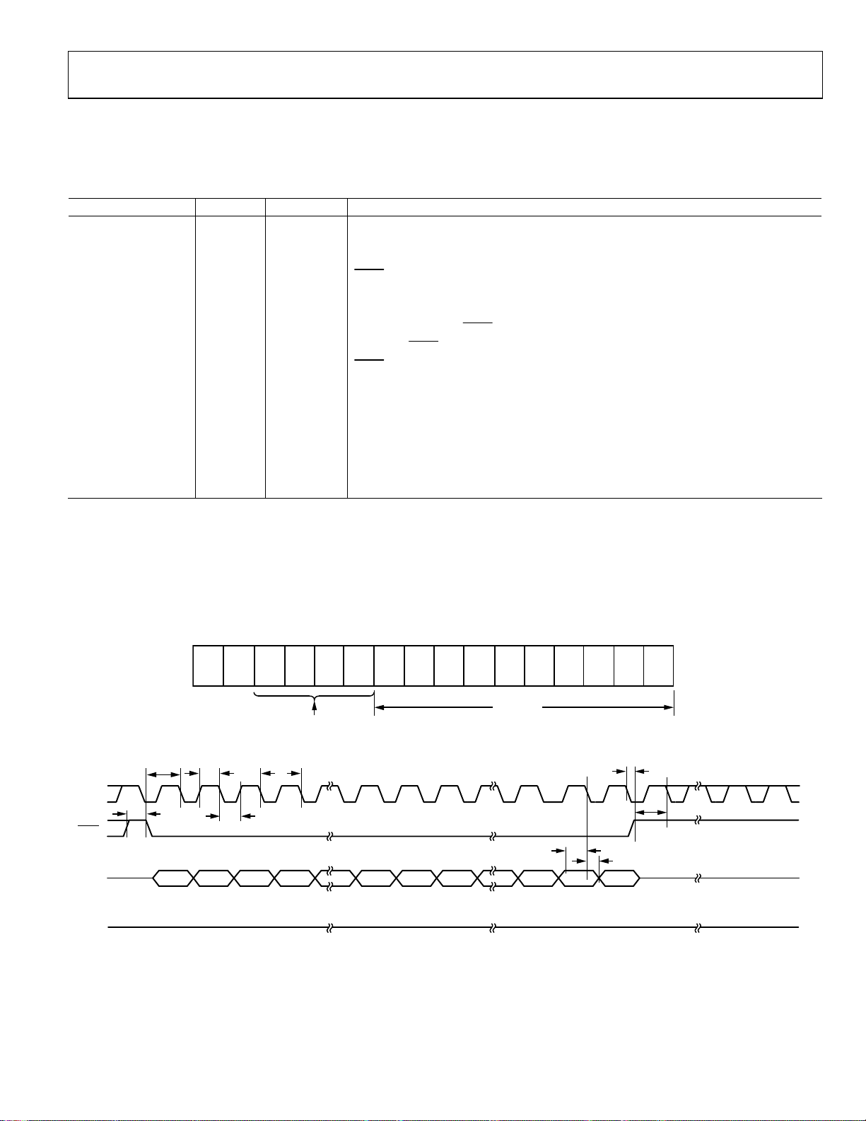
Shift Register and Timing Diagrams
DB9 (MSB) DB0 (LSB)
to T
MIN
MAX
rising edge
, unless otherwise noted.
SCLK
SYNC
DIN
SDO
C0C1
C3
00
C2
CONTROL BI TS
D9
D7 D6 D5 D4 D3
D8
DATA BITS
Figure 2. Shift Register Content
t
4
t
8
t
2
t
3
0 0 C3 C2 D7 D6 D5 D2 D1 D0
t
1
Figure 3. Write Timing Diagram (CPOL = 0, CPHA = 1)
Rev. E | Page 7 of 24
t
5
D2 D1
t
6
D0
08077-002
t
7
t
9
08077-003
AD5270/AD5271
SCLK
SYNC
t
9
DIN
SDO
00 00C3 C3
X X C3 D1 D0
Figure 4. Read Timing Diagram (CPOL = 0, CPHA = 1)
D1 D0D0 D0
t
10
08077-004
Rev. E | Page 8 of 24

AD5270/AD5271
ABSOLUTE MAXIMUM RATINGS
TA = 25°C, unless otherwise noted.
Table 8.
Parameter Rating
VDD to GND –0.3 V to +7.0 V
VSS to GND +0.3 V to −7.0 V
VDD to VSS 7 V
VA, VW to GND VSS − 0.3 V, VDD + 0.3 V
Digital Input and Output Voltage to GND −0.3 V to VDD + 0.3 V
EXT_CAP to VSS 7 V
IA, IW
Continuous
RAW = 20 kΩ ±3 mA
RAW = 50 kΩ, 100 kΩ ±2 mA
Pulsed1
Frequency > 10 kHz ±MCC2/d3
Frequency ≤ 10 kHz ±MCC2/√d3
Operating Temperature Range4 −40°C to +125°C
Maximum Junction Temperature
(T
Maximum)
J
150°C
Storage Temperature Range −65°C to +150°C
Reflow Soldering
Peak Temperature 260°C
Time at Peak Temperature 20 sec to 40 sec
Package Power Dissipation (TJ max − TA)/θJA
1
Maximum terminal current is bounded by the maximum current handling of
the switches, maximum power dissipation of the package, and maximum
applied voltage across any two of the A and W terminals at a given
resistance.
2
Maximum continuous current.
3
Pulse duty factor.
4
Includes programming of 50-TP memory.
Stresses above those listed under Absolute Maximum Ratings
may cause permanent damage to the device. This is a stress
rating only and functional operation of the device at these or
any other conditions above those indicated in the operational
section of this specification is not implied. Exposure to absolute
maximum rating conditions for extended periods may affect
device reliability.
THERMAL RESISTANCE
θJA is defined by JEDEC specification JESD-51 and the value is
dependent on the test board and test environment.
Table 9. Thermal Resistance
Package Type θ
1
θJC Unit
JA
10-Lead LFCSP 50 3 °C/W
10-Lead MSOP 135 N/A °C/W
1
JEDEC 2S2P test board, still air (0 m/s air flow).
ESD CAUTION
Rev. E | Page 9 of 24

AD5270/AD5271
1
2
3
4
PIN CONFIGURATION AND FUNCTION DESCRIPTIONS
10
9
8
7
6
SYNC
SCLK
DIN
SDO
GND
VDD1
2
1
V
V
EXT_CAP
DD
A
W
SS
AD5270/
2
AD5271
3
TOP VIEW
4
(Not toScale)
5
10
9
8
7
6
Figure 5. MSOP Pin Configuration
SYNC
SCLK
DIN
SDO
GND
A
W
V
SS
EXT_CAP
NOTES
1.THE EXPOSED PAD IS LEFT FLOATING
08077-005
OR IS TIED TO V
Figure 6. LFCSP Pin Configuration
AD5270/
AD5271
3
(EXPOSED
4
5
PAD)
.
SS
Table 10. Pin Function Descriptions
Pin No. Mnemonic Description
1 VDD Positive Power Supply. Decouple this pin with 0.1 μF ceramic capacitors and 10 μF capacitors.
2 A Terminal A of RDAC. VSS ≤ VA ≤ VDD.
3 W Wiper Terminal of RDAC. VSS ≤ VW ≤ VDD.
4 VSS
Negative Supply. Connect to 0 V for single-supply applications. Decouple this pin with 0.1 μF ceramic
capacitors and 10 μF capacitors.
5 EXT_CAP
External Capacitor. Connect a 1 μF capacitor between EXT_CAP and V
. This capacitor must have a voltage
SS
rating of ≥7 V.
6 GND Ground Pin, Logic Ground Reference.
7 SDO
Serial Data Output. This pin can be used to clock data from the shift register in daisy-chain mode or in
readback mode. This open-drain output requires an external pull-up resistor even if it is not use.
8 DIN
Serial Data Line. This pin is used in conjunction with the SCLK line to clock data into or out of the 16-bit input
register.
9 SCLK
Serial Clock Input. Data is clocked into the shift register on the falling edge of the serial clock input. Data can
be transferred at rates up to 50 MHz.
10
Falling Edge Synchronization Signal. This is the frame synchronization signal for the input data. When SYNC
SYNC
goes low, it enables the shift register and data is transferred in on the falling edges of the subsequent clocks.
The selected register is updated on the rising edge of SYNC following the 16th clock cycle. If SYNC is taken
high before the 16th clock cycle, the rising edge of SYNC acts as an interrupt, and the write sequence is
ignored by the RDAC.
EPAD Exposed Pad Leave floating or connected to VSS.
08077-040
Rev. E | Page 10 of 24

AD5270/AD5271
TYPICAL PERFORMANCE CHARACTERISTICS
0.8
0.6
+125°C
+25°C
–40°C
RAW = 20kΩ
0.8
0.6
TA = 25°C
20kΩ
50kΩ
100kΩ
0.4
0.2
INL (LSB)
0
–0.2
–0.4
0 128 256 384 512 640 768 896 1023
CODE (Decimal)
Figure 7. R-INL in R-Perf Mode vs. Code vs. Temperature (AD5270)
0.2
0.1
0
–0.1
–0.2
DNL (LSB)
–0.3
–0.4
–0.5
–0.6
0 128 256 384 512 640 768 896 1023
–40°C
+25°C
CODE (Decimal)
RAW = 20kΩ
+125°C
Figure 8. R-DNL in R-Perf Mode vs. Code vs. Temperature (AD5270)
0.50
0.40
+125°C
+25°C
–40°C
RAW = 20kΩ
0.4
0.2
INL (LSB)
0
–0.2
–0.4
0 256 512 768 1023
08077-010
CODE (Decimal)
08077-111
Figure 10. R-INL in R-Perf Mode vs. Code vs. Nominal Resistance (AD5270)
0.6
TA = 25°C
0.4
0.2
0
DNL (LSB)
–0.2
–0.4
–0.6
08077-011
20kΩ 50kΩ 100kΩ
0 256 512 768 1023
CODE (Decimal)
08077-120
Figure 11. R-DNL in R-Perf Mode vs. Code vs. Nominal Resistance (AD5270)
0.6
0.4
TA = 25°C
20kΩ
50kΩ
100kΩ
0.30
0.20
INL (LSB)
0.10
0
–0.10
0 128 256 384 512 640 768 896 1023
CODE (Decimal)
Figure 9. R-INL in Normal Mode vs. Code vs. Temperature (AD5270)
08077-014
Figure 12. R-INL in Normal Mode vs. Code vs. Nominal Resistance (AD5270)
Rev. E | Page 11 of 24
0.2
INL (LSB)
0
–0.2
–0.4
0 256 512 768 1023
CODE (Decimal)
08077-121

AD5270/AD5271
0.15
0.10
+125°C
+25°C
–40°C
RAW = 20kΩ
0.15
0.10
TA = 25°C
20kΩ
50kΩ
100kΩ
0.05
0
DNL (LSB)
–0.05
–0.10
–0.15
0 128 256 384 512 640 768 896 1023
CODE (Decimal)
Figure 13. R-DNL in Normal Mode vs. Code vs. Temperature (AD5270)
0.20
0.15
0.10
0.05
INL (LSB)
–0.05
+125°C
+25°C
–40°C
0
RAW = 20kΩ
0.05
0
–0.05
DNL (LSB)
–0.10
–0.15
–0.20
0 256 512 768 1023
08077-015
CODE (Dec imal)
8077-122
Figure 16. R-DNL in Normal Mode vs. Code vs. Nominal Resistance (AD5270)
0.15
INL (LSB)
TA = 25°C
0.10
0.05
0
–0.05
20kΩ
100kΩ
–0.10
0 64 128 192 255
CODE (Decimal)
Figure 14. R-INL in R-Perf Mode vs. Code vs. Temperature (AD5271)
0.06
RAW = 20kΩ
0.04
0.02
0
–0.02
–0.04
DNL (LSB)
–0.06
–0.08
–0.10
–0.12
–0.14
0 64 128 192 255
CODE (Decimal)
+125°C
+25°C
–40°C
Figure 15. R-DNL in R-Perf Mode vs. Code vs. Temperature (AD5271)
–0.10
0 64 128 192 255
08077-013
CODE (Decimal)
08077-123
Figure 17. R-INL in R-Perf Mode vs. Code vs. Nominal Resistance (AD5271)
0.15
TA = 25°C
0.10
0.05
0
DNL (LS B)
–0.05
–0.10
–0.15
08077-012
20kΩ 100kΩ
0 64 128 192 255
CODE (Decimal)
08077-125
Figure 18. R-DNL in R-Perf Mode vs. Code vs. Nominal Resistance (AD5271)
Rev. E | Page 12 of 24

AD5270/AD5271
0.10
0.08
+125°C
+25°C
–40°C
RAW = 20kΩ
0.15
0.10
TA = 25°C
20kΩ
100kΩ
0.06
0.04
INL (LSB)
0.02
0
–0.02
0 64 128 192 255
CODE (Decimal)
Figure 19. R-INL in Normal Mode vs. Code vs. Temperature (AD5271)
DNL (LSB)
0.03
0.02
0.01
–0.01
–0.02
RAW = 20kΩ
0
+125°C
+25°C
–40°C
0.05
INL (LSB)
0
–0.05
–0.10
0 64 128 192 255
08077-016
CODE (Decimal)
08077-126
Figure 22. R-INL in Normal Mode vs. Code vs. Nominal Resistance (AD5271)
DNL (LSB)
0.010
0.008
0.006
0.004
0.002
100kΩ
20kΩ
0
TA = 25°C
–0.03
0 64 128 192 255
CODE (Decimal)
Figure 20. R-DNL in Normal Mode vs. Code vs. Temperature (AD5271)
500
400
300
200
100
0
–100
CURRENT (nA)
–200
–300
–400
–500
–40 –30 –20 –10 0 20 30 40 50 60 70 80 90 100 11010
Figure 21. Supply Current (I
ISS = 3V
TEMPERATURE (°C)
IDD = 5V
IDD = 3V
ISS = 5V
, ISS) vs. Temperature
DD
–0.002
0 64 128 192 255
08077-017
CODE (Decimal)
08077-027
Figure 23. R-DNL in Normal Mode vs. Code vs. Nominal Resistance (AD5271)
1.0
0.8
0.6
0.4
CURRENT (mA)
0.2
0
0 0.5 1. 0 1.5 2.0 2.5 3.0 3.5 4.0 4.5 5.0 5.5
08077-018
Figure 24. Supply Current I
VOLTAGE (V)
vs. Digital Input Voltage
DD
8077-023
Rev. E | Page 13 of 24
AD5270/AD5271
50
45
40
35
30
25
20
15
10
RHEOST AT MODE TEMPCO (pp m/°C)
5
0
0 256 512 768 1023
0 64 128 192 255
0
0x200 (0x80)
0x100 (0x40)
–10
0x080 (0x20)
–20
0x040 (0x10)
0x020 (0x08)
–30
0x010 (0x04)
GAIN (dB)
0x008 (0x02)
–40
0x004 (0x01)
0x002
–50
0x001
–60
1k
CODE (Decimal)
Figure 25. Tempco ΔR
10k
100k 1M 10M
FREQUENCY (Hz )
/ΔT vs. Code
WA
VDD/VSS= 5V/0V
20kΩ
50kΩ
100kΩ
AD5270 (AD5271)
AD5270
AD5271
7
6
5
(mA)
4
WA_MAX
3
2
THEORETICAL I
1
0
0 256 512 768 1023
8077-019
0 64 128 192 255
CODE (Decimal)
VDD/VSS=5V/0V
20kΩ
50kΩ
100kΩ
AD5270
AD5271
08077-028
Figure 28. Theoretical Maximum Current vs. Code
0
0x200 (0x80)
0x100 (0x40)
–10
0x080 (0x20)
–20
0x040 (0x10)
0x020 (0x08)
–30
0x010 (0x04)
0x008 (0x02)
–40
GAIN (dB)
0x004 (0x01)
–50
0x002
0x001
–60
–70
1k
08077-031
10k
100k 1M 10M
FREQUENCY (Hz)
AD5270 (AD5271)
08077-041
–10
–20
–30
GAIN (dB)
–40
–50
–60
Figure 26. 20 kΩ Gain vs. Code vs. Frequency
0
0x200 (0x80)
0x100 (0x40)
0x080 (0x20)
0x040 (0x10)
0x020 (0x08)
0x010 (0x04)
0x008 (0x02)
0x004 (0x01)
0x002
0x001
1k
10k
100k 1M 10M
FREQUENCY (Hz )
Figure 27. 50 kΩ Gain vs. Code vs. Frequency
AD5270 (AD5271)
08077-032
Rev. E | Page 14 of 24
Figure 29. 100 kΩ Gain vs. Code vs. Frequency
0
VDD /VSS= 5V/0V
CODE = HALF SCAL E
–10
–20
–30
–40
–50
PSRR (dB)
–60
–70
–80
–90
50kΩ
100kΩ
20kΩ
100 1k 10k 100k
FREQUENCY (Hz )
Figure 30. PSRR vs. Frequency
08077-024

AD5270/AD5271
0
VDD/VSS= 5V/0V
CODE = HAL F SCALE
NOISE BW = 22kHz
V
–20
IN
–40
–60
THD + N (dB)
–80
–100
100
= 1V rms
1k
FREQUENCY (Hz)
Figure 31. THD + N vs. Frequency
10k
20kΩ
50kΩ
100kΩ
100k
08077-025
0
–10
–20
–30
–40
–50
THD + N (dB)
–60
–70
–80
–90
–100
0.001 0.01 0. 1 1
VOLTAGE (V
VDD/VSS = 5V/0V
CODE = HALF SCALE
f
= 1kHz
IN
NOISE BW = 22kHz
)
RMS
Figure 34. THD + N vs. Amplitude
20kΩ
50kΩ
100kΩ
08077-026
0.03
0.02
0.01
20kΩ
50kΩ
100kΩ
0
0.0010
0.0005
VDD/VSS = 5V/0V
I
= 200µA
AW
CODE = HALF SCAL E
0
–0.01
VOLTAGE (V)
–0.02
–0.03
–0.04
–1 4 9 14 19
TIME (µs)
Figure 32. Maximum Glitch Energy
45
40
35
30
25
20
15
10
NUMBER OF CODES (AD5270)
5
0
2.7 3.2 3.7 4.2 4.7 5.2
VDD (V)
T
A
= 25°C
20kΩ
50kΩ
100kΩ
11.25
10.00
8.75
7.50
6.25
5.00
3.75
2.50
1.25
0
08077-043
NUMBER OF CODES (AD5271)
8077-021
–0.0005
VOLTAGE (V)
–0.0010
–0.0015
0–10 10 20 30 40 50 60
TIME (µs)
Figure 35. Digital Feedthrough
70
60
50
40
30
20
NUMBER OF CODES (AD5270)
10
0
–40 –20 0 20 40 60 80 100 120
TEMPERATURE (°C)
VDD/VSS= 5V/0V
20kΩ
50kΩ
100kΩ
15.5
15.0
12.5
10.0
7.5
5.0
2.5
0
08077-046
NUMBER OF CODES (AD5271)
08077-020
Figure 33. Maximum Code Loss vs. Voltage
Figure 36. Maximum Code Loss vs. Temperature
Rev. E | Page 15 of 24

AD5270/AD5271
R
8
7
0.006
0.005
0.004
0.003
VDD/VSS = 5V/0V
I
= 10µA
AW
CODE = HALF SCAL E
6
VOLTAGE (V)
5
4
0.07 0.09 0. 11 0.13 0.15 0.17
Figure 37. V
TIME (Seco nds)
Waveform While Writing Fuse
EXT_CAP
0.002
RESISTANCE (%)
0.001
AW
∆
0
–0.001
–0.002
01900800700600500400300200100
8077-029
OPERATIO N AT 150°C (Ho urs)
000
08077-038
Figure 38. Long-Term Drift Accelerated Average by Burn-In
Rev. E | Page 16 of 24

AD5270/AD5271
V
V
%
TEST CIRCUITS
Figure 39 to Figure 43 define the test conditions used in the Specifications section.
DUT
W
A
I
W
V
MS
08077-033
Figure 39. Resistor Position Nonlinearity Error
(Rheostat Operation; R-INL, R-DNL)
DUT
W
A
1GΩ
V
V
MS
Figure 42. Gain vs. Frequency
08077-036
MS
RWA =
I
W
CODE = 0x00
DUT
W
A
V
MS
R
RW =
WA
2
08077-034
I
W
Figure 40. Wiper Resistance
+ = VDD ±10
PSRR (dB) = 20 L OG
I
W
V
DD
V+
W
A
V
PSS (%/%) =
MS
∆VMS%
∆V
DD
V
MS
V
DD
%
08077-035
DUT
I
CM
W
A
NC
+2.75V –2.75V
GND
Figure 43. Common Leakage Current
GND
GND
NC = NO CONNECT
+2.75V
–2.75V
08077-037
Figure 41. Power Supply Sensitivity (PSS, PSRR)
Rev. E | Page 17 of 24

AD5270/AD5271
THEORY OF OPERATION
The AD5270 and AD5271 are designed to operate as true
variable resistors for analog signals within the terminal voltage
range of V
mine the resistor wiper position. The RDAC register acts as a
scratchpad register, which allows unlimited changes of resistance
settings. The RDAC register can be programmed with any position
setting using the SPI interface. When a desirable wiper position
is found, this value can be stored in a 50-TP memory register.
Thereafter, the wiper position is always restored to that position
for subsequent power-up. The storing of 50-TP data takes approximately 350 ms; during this time, the AD5270/AD5271 lock to
prevent any changes from taking place.
The AD5270/AD5271 also feature a patented 1% end-to-end
resistor tolerance. This simplifies precision, rheostat mode, and
open-loop applications where knowledge of absolute resistance
is critical.
SERIAL DATA INTERFACE
The AD5270/AD5271 contain a serial interface (
DIN , and SDO), which is compatible with SPI interface standards,
as well as most DSPs. This device allows writing of data via the
serial interface to every register.
SHIFT REGISTER
For the AD5270/AD5271, the shift register is 16 bits wide, as
shown in Figure 2. The 16-bit word consists of two unused bits,
which should be set to zero, followed by four control bits and
10 RDAC data bits (note that for the AD5271 only, the lower
two RDAC data bits are don’t care if the RDAC register is read
from or written to). Data is loaded MSB first (Bit 15). The four
control bits determine the function of the software command as
listed in Table 1 1. Figure 3 shows a timing diagram of a typical
AD5270/AD5271 write sequence.
The write sequence begins by bringing the
SYNC
loaded from the DIN pin. When
data-word is decoded according to the instructions in .
The command bits (Cx) control the operation of the digital
potentiometer. The data bits (Dx) are the values that are loaded
into the decoded register. The AD5270/AD5271 have an internal
counter that counts a multiple of 16 bits (a frame) for proper
operation. For example, AD5270/AD5271 each works with a
32-bit word but do not work properly with a 31-bit or 33-bit
word. The AD5270/AD5271 do not require a continuous SCLK
when
digital input buffers, operate all serial interface pins close to the
V
DD
< V
SS
pin must be held low until the complete data-word is
SYNC
supply rails.
< VDD. The RDAC register contents deter-
TERM
SYNC
SYNC
line low. The
SYNC
returns high, the serial
is high. To minimize power consumption in the
, SCLK,
Tabl e 11
RDAC REGISTER
The RDAC register directly controls the position of the digital
rheostat wiper. For example, when the RDAC register is loaded
with all zeros, the wiper is connected to Terminal A of the variable
resistor. The RDAC register is a standard logic register and
there is no restriction on the number of changes allowed. The
basic mode of setting the variable resistor wiper position
(programming the RDAC register) is accomplished by loading
the serial data input register with Command 1 (see Ta b le 1 1 ) and
with the desired wiper position data.
50-TP MEMORY BLOCK
The AD5270/AD5271 contain an array of 50-TP programmable
memory registers, which allow the wiper position to be programmed up to 50 times. Table 13 shows the memory map.
When the desired wiper position is determined, the user can
load the serial data input register with Command 3 (see Ta bl e
11) which stores the wiper position data in a 50-TP memory
register. The first address to be programmed is Location 0x01
(see Table 13); the AD5270/AD5271 increments the 50-TP
memory address for each subsequent program until the memory
is full. Programming data to 50-TP consumes approximately
4 mA for 55 ms, and takes approximately 350 ms to complete,
during which time the shift register locks to prevent any changes
from occurring. Bit C3 of the control register can be polled to
verify that the fuse program command was completed properly.
No change in supply voltage is required to program the 50-TP
memory; however, a 1 μF capacitor on the EXT_CAP pin is
required (see Figure 46). Prior to 50-TP activation, the AD5270
and the AD5271 preset to midscale on power up.
WRITE PROTECTION
At power-up, the serial data input register write commands for
both the RDAC register and the 50-TP memory registers are
disabled. The RDAC write protect bit, C1, of the control register
(see Tabl e 13 and Ta bl e 14 ) is set to 0 by default. This disables
any change of the RDAC register content regardless of the
software commands, except that the RDAC register can be
refreshed from the 50-TP memory using the software reset,
Command 4. To enable programming of the RDAC register, the
write protect bit (Bit C1), of the control register must first be
programmed by loading the serial data input register with
Command 7. To enable programming of the 50-TP memory,
the program enable bit (Bit C0) of the control register, which is
set to 0 by default, must first be set to 1.
Rev. E | Page 18 of 24
AD5270/AD5271
RDAC AND 50-TP READ OPERATION
A serial data output SDO pin is available for readback of the
internal RDAC register or 50-TP memory contents. The
contents of the RDAC register can be read back through SDO
by using Command 2 (see Tabl e 1 1 ). Data from the RDAC
register is clocked out of the SDO pin during the last 10 clocks
of the next SPI operation.
It is possible to read back the contents of any of the 50-TP
memory registers through SDO by using Command 5. The
lower six LSB bits, D0 to D5 of the data byte, select which
memory location is to be read back, as shown in Table 13.
Table 11. Command Operation Truth Table
Command
Number
0 0 0 0 0 X X X X X X X X X X NOP: do nothing.
1 0 0 0 1 D9 D8 D7 D6 D5 D4 D3 D2 D12 D0
2 0 0 1 0 X X X X X X X X X X
3 0 0 1 1 X X X X X X X X X X
4 0 1 0 0 X X X X X X X X X X
53 0 1 0 1 X X X X D5 D4 D3 D2 D1 D0
6 0 1 1 0 X X X X X X X X X X
74 0 1 1 1 X X X X X X X D2 D1 D0
8 1 0 0 0 X X X X X X X X X X Read contents of control register.
9 1 0 0 1 X X X X X X X X X D0 Software shutdown.
D0 = 0; normal mode.
1
X is don’t care.
2
AD5271 = don’t care.
3
See Table 15 for 50-TP memory map.
4
See Table 14 for bit details.
Command[DB13:DB10] Data[DB9:DB0]1
C3 C2 C1 C0 D9 D8 D7 D6 D5 D4 D3 D2 D1 D0
Data from the selected memory location is clocked out of the
SDO pin during the next SPI operation. A binary encoded
version address of the most recently programmed wiper memory
location can be read back using Command 6 (see Table 11 ). This
can be used to monitor the spare memory status of the 50-TP
memory block.
Tabl e 1 2 provides a sample listing for the sequence of serial data
input (DIN) words with the serial data output appearing at the
SDO pin in hexadecimal format for a write and read to both the
RDAC register and the 50-TP memory (Memory Location 20).
Operation
2
Write contents of serial register
data to RDAC.
Read contents of RDAC wiper
register.
Store wiper setting: store RDAC
setting to 50-TP.
Software reset: refresh RDAC with
last 50-TP memory stored value.
Read contents of 50-TP from SDO
output in the next frame.
Read address of last 50-TP
programmed memory location.
Write contents of serial register
data to control register.
D0 = 1; device placed in shutdown
mode.
Rev. E | Page 19 of 24
AD5270/AD5271
SHUT-DOWN MODE
The AD5270/AD5271 can be shut down by executing the
software shutdown command, Command 9 (see Tab l e 11 ), and
setting the LSB to 1. This feature places the RDAC in a zeropower-consumption state where Terminal Ax is open circuited
and the Wiper Terminal Wx remains connected. It is possible to
execute any command from Ta b le 11 while the AD5270/AD5271
are in shutdown mode. The parts can be taken out of shutdown
mode by executing Command 9 and setting the LSB to 0 or by a
software reset, Command 4 (see Ta b le 1 1 ).
Table 12. Write and Read to RDAC and 50-TP Memory
DIN SDO1 Action
0x1C03 0xXXXX Enable update of the wiper position and the 50-TP memory contents through the digital interface.
0x0500 0x1C03 Write 0x100 to the RDAC register; wiper moves to ¼ full-scale position.
0x0800 0x0500 Prepares data read from RDAC register.
0x0C00 0x100
0x1800 0x0C00 Prepares data read of last programmed 50-TP memory monitor location.
0x0000 0xXX19
0x1419 0x0000 Prepares data read from Memory Location 0x19.
0x2000 0x0100
0x0000 0xXXXX
1
X is don’t care.
Table 13. Control Register Bit Map
DB9 DB8 DB7 DB6 DB5 DB4 DB3 DB2 DB1 DB0
0 0 0 0 0 0 C3 C2 C1 C0
Stores RDAC register content into the 50-TP memory. A 16-bit word appears out of SDO, where the last 10-bits contain
the contents of the RDAC register (0x100).
NOP Instruction 0 sends a 16-bit word out of SDO, where the six LSBs last six bits contain the binary address of the last
programmed 50-TP memory location, for example, 0x19 (see Table 13).
Prepares data read from the control register. Sends a 16-bit word out of SDO, where the last 10-bits contain the
contents of Memory Location 0x19.
NOP Instruction 0 sends a 16-bit word out of SDO, where the last four bits contain the contents of the control register.
If Bit C3 = 1, the fuse program command successful.
RESISTOR PERFORMANCE MODE
This mode activates a new, patented 1% end-to-end resistor
tolerance that ensures a ±1% resistor tolerance error on each
code, that is, code = half scale, R
= 10 kΩ ± 100 Ω. See Tabl e 2 ,
WA
Tabl e 3 , Ta bl e 5, and Ta ble 6 to verify which codes achieve ±1%
resistor tolerance. The resistor performance mode is activated by
programming Bit C2 of the control register.
RESET
The AD5270/AD5271 can be reset through software by executing
Command 4 (see Tabl e 11 ). The reset command loads the
RDAC register with the contents of the most recently programmed
50-TP memory location. The RDAC register loads with
midscale if no 50-TP memory location has been previously
programmed.
Table 14. Control Register Bit Description
Bit Name Description
C0 50-TP program enable
0 = 50-TP program disabled (default)
1 = enable device for 50-TP program
C1 RDAC register write protect
0 = wiper position frozen to value in 50-TP memory (default)1
1 = allow update of wiper position through digital interface
C2 R-performance enable
0 = RDAC resistor tolerance calibration enabled (default)
1 = RDAC resistor tolerance calibration disabled
C3 50-TP memory program success bit
0 = fuse program command unsuccessful (default)
1 = fuse program command successful
1
Wiper position frozen to the last value programmed in the 50-TP memory. The wiper is frozen to midscale if the 50-TP memory has not been previously programmed.
Rev. E | Page 20 of 24

AD5270/AD5271
V
A
Table 15. Memory Map
Data Byte[DB9:DB8]1
Command Number
5
D9 D8 D7 D6 D5 D4 D3 D2 D1 D0
X X X 0 0 0 0 0 0 0 Reserved
X X X 0 0 0 0 0 0 1 1st programmed wiper location (0x01)
X X X 0 0 0 0 0 1 0 2nd programmed wiper location (0x02)
X X X 0 0 0 0 0 1 1 3rd programmed wiper location (0x03)
X X X 0 0 0 0 1 0 0 4th programmed wiper location (0x04)
… … … … … … … … … … …
X X X 0 0 0 1 0 1 0 10th programmed wiper location (0xA)
X X X 0 0 1 0 1 0 0 20th programmed wiper location (0x14)
X X X 0 0 1 1 1 1 0 30th programmed wiper location (0x1E)
X X X 0 1 0 1 0 0 0 40th programmed wiper location (0x28)
X X X 0 1 1 0 0 1 0 50th programmed wiper location (0x32)
1
X is don’t care.
SDO PIN AND DAISY-CHAIN OPERATION
The serial data output pin (SDO) serves two purposes: it can be
used to read the contents of the wiper setting and 50-TP values
using Command 2 and Command 5, respectively (see Ta b le 1 1),
or the SDO pin can be used in daisy-chain mode. Data is clocked
out of SDO on the rising edge of SCLK. The SDO pin contains
an open-drain N-channel FET that requires a pull-up resistor.
To place the pin in high impedance and mini-mize the power
dissipation when the pin is used, the 0x8001 data word followed
by Command 0 should be sent to the part. Tab le 1 6 provides a
sample listing for the sequence of the serial data input (DIN).
Daisy chaining minimizes the number of port pins required
from the controlling IC. As shown in Figure 44, the user must
tie the SDO pin of one package to the DIN pin of the next
package. The user may need to increase the clock period because
the pull-up resistor and the capacitive loading at the SDO-toDIN interface may require additional time delay between
subsequent devices. When two AD5270/AD5271 devices are
daisy-chained, 32 bits of data are required. The first 16 bits go to
U2, and the second 16 bits go to U1.
µC
RDAC ARCHITECTURE
To achieve optimum performance, Analog Devices has patented
the RDAC segmentation architecture for all the digital potentiometers. In particular, the AD5270/AD5271 employ a three-stage
segmentation approach as shown in Figure 45.The AD5270/
AD5271 wiper switch is designed with the transmission gate
CMOS topology.
Register Contents
DD
AD5270/
AD5271
SYNC
U1
SDO
SCLK
MOSI
SSSCLK
Figure 44. Daisy-Chain Configuration Using SDO
R
R
2.2kΩ
L
P
AD5270/
AD5271
U2
DINDIN SDO
SYNC
SCLK
08077-006
Table 16. Minimize Power Dissipation at the SDO Pin
DIN SDO1 Action
0xXXXX 0xXXXX Last user command sent to the digipot.
0x8001 0xXXXX
Prepares the SDO pin to be placed in
high impedance mode.
0x0000
1
X is don’t care.
Keep the
respective serial registers. The
High
Impedance
SYNC
pin low until all 32 bits are clocked to their
The SDO pin is placed in high
impedance.
SYNC
pin is then pulled high to
8-/10-BIT
ADDRESS
DECODER
Figure 45. Simplified RDAC Circuit
R
L
R
M
S
W
R
M
R
W
W
R
W
08077-007
complete the operation.
Rev. E | Page 21 of 24
AD5270/AD5271
V
PROGRAMMING THE VARIABLE RESISTOR
Rheostat Operation—1% Resistor Tolerance
The nominal resistance between Terminal W and Terminal A, RWA,
is 20 kΩ, 50 kΩ, or 100 kΩ and has 1024-/256-tap points accessed
by the wiper terminal. The 10-/8-bit data in the RDAC latch is
decoded to select one of the 1024 or 256 possible wiper settings.
The AD5270 and AD5271 contain an internal ±1% resistor
tolerance calibration feature that can be disabled or enabled,
enabled by default, or by programming Bit C2 of the control
register (see Ta b le 1 3 and Ta b le 1 4).
The digitally programmed output resistance between the W
terminal and the A terminal, R
maximum of ±1% absolute resistance error over both the full
supply and temperature ranges. As a result, the general
equations for determining the digitally programmed output
resistance between the W terminal and the A terminal are the
following:
For the AD5270
D
1024
R
WAWA
DR ×=
)(
For the AD5271
D
256
R
WAWA
DR ×=
)(
where:
D is the decimal equivalent of the binary code loaded in the
10-/8-bit RDAC register.
R
is the end-to-end resistance.
WA
In the zero-scale condition, a finite total wiper resistance of
120 Ω is present. Regardless of which setting the part is operating in, take care to limit the current between Terminal A to
Terminal W to the maximum continuous current of ±3 mA or
a pulse current specified in Tab le 8 . Otherwise, degradation or
possible destruction of the internal switch contact can occur.
EXT_CAP CAPACITOR
A 1 μF capacitor to VSS must be connected to the EXT_CAP
pin, as shown in Figure 46, on power-up and throughout the
operation of the AD5270/AD5271.
EXT_CAP
C1
1µF
, is calibrated to give a
WA
(1)
(2)
AD5270/
AD5271
50_OTP
MEMORY
BLOCK
V
SS
TERMINAL VOLTAGE OPERATING RANGE
The positive VDD and negative VSS power supplies of the
AD5270/AD5271 define the boundary conditions for proper
2-terminal digital resistor operation. Supply signals present on
Ter m in a l A a nd Te rm i na l W t h at e x ce e d V
or VSS are clamped
DD
by the internal forward-biased diodes, see Figure 47.
DD
A
W
V
SS
08077-009
Figure 47. Maximum Terminal Voltages Set by V
DD
and V
SS
The ground pins of the AD5270/AD5271 devices are primarily
used as digital ground references. To minimize the digital ground
bounce, join the AD5270/AD5271 ground terminal remotely
to the common ground. The digital input control signals to the
AD5270/AD5271 must be referenced to the device ground pin
(GND), and must satisfy the logic level defined in the
Specifications section. An internal level shift circuit ensures that
the common-mode voltage range of the three terminals extends
from V
to VDD, regardless of the digital input level.
SS
POWER-UP SEQUENCE
Because there are diodes to limit the voltage compliance at
Ter m in a l A a nd Te rm i na l W ( s ee Figure 47), it is important to
power V
and Terminal W; otherwise, the diode is forward-biased such
that V
DD/VSS
sequence is V
order of powering V
important as long as they are powered after V
As soon as V
first sets the RDAC to midscale and then restores the last programmed 50-TP value to the RDAC register.
first before applying any voltage to Terminal A
DD/VSS
are powered unintentionally. The ideal power-up
, GND, VDD, digital inputs, VA, and VW. The
SS
, VW, and the digital inputs is not
A
.
DD/VSS
is powered, the power-on preset activates which
DD
V
SS
Figure 46. EXT_CAP Hardware Setup
08077-008
Rev. E | Page 22 of 24
AD5270/AD5271
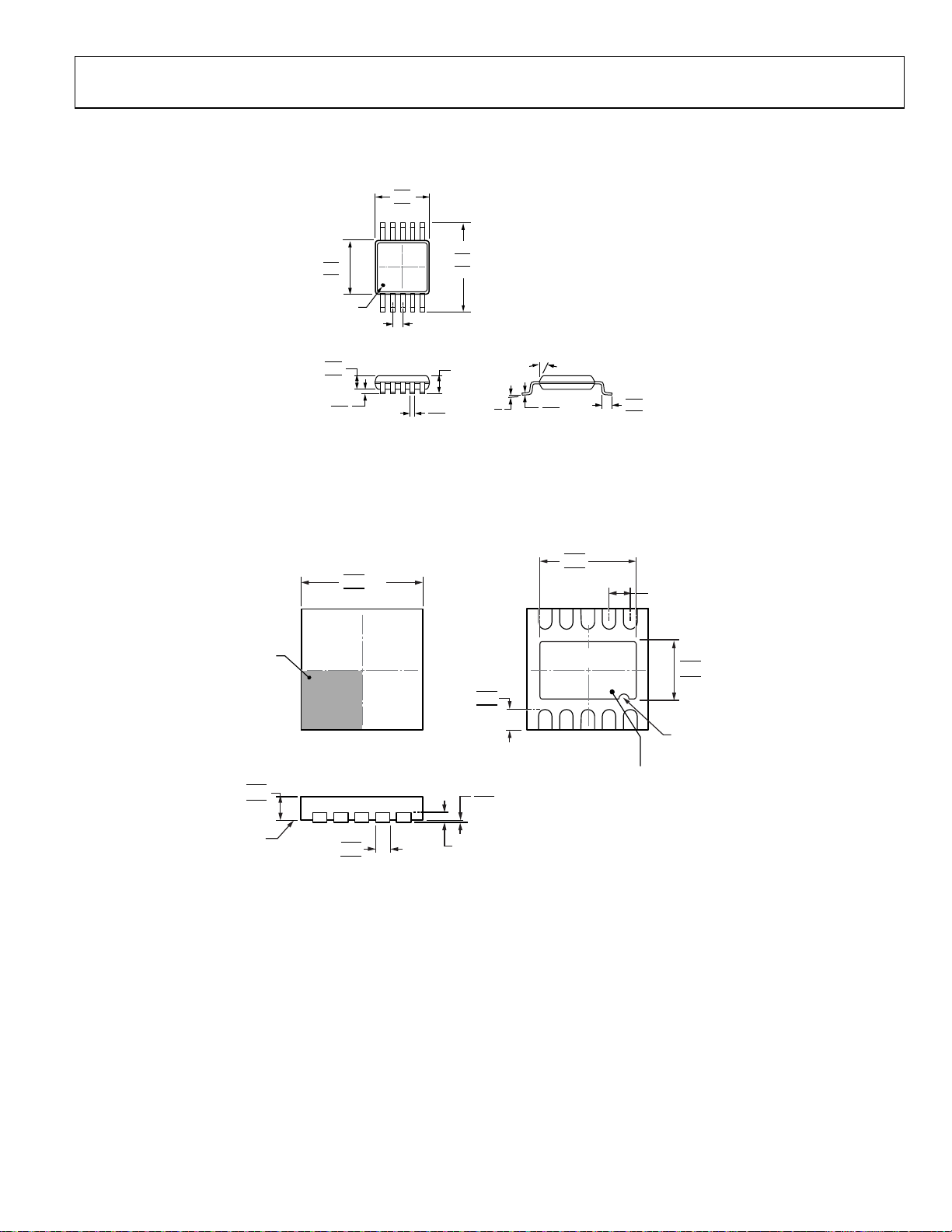
OUTLINE DIMENSIONS
3.10
3.00
2.90
10
6
3.10
3.00
2.90
PIN 1
IDENTIFIER
0.95
0.85
0.75
0.15
0.05
COPLANARITY
1
0.50 BSC
0.10
COMPLIANT TO JEDEC STANDARDS MO-187-BA
Figure 48. 10-Lead Mini Small Outline Package [MSOP]
3.10
3.00 SQ
2.90
5.15
4.90
4.65
5
15° MAX
6°
0°
0.23
0.13
0.30
0.15
1.10 MAX
(RM-10)
Dimensions shown in millimeters
2.48
2.38
2.23
0.70
0.55
0.40
091709-A
0.50 BSC
PIN 1 INDEX
AREA
0.80
0.75
0.70
SEATING
PLANE
6
EXPOSED
PAD
0.50
0.40
TOP VIEW
0.30
0.25
0.30
0.05 MAX
0.02 NOM
0.20 REF
5
BOTTOM VIEW
FOR PROPER CONNECTION OF
THE EXPOSED PAD, REFER TO
THE PIN CONFIGURATION AND
FUNCTION DESCRIPTIONS
SECTION OF THIS DATA SHEET.
0.20
Figure 49. 10-Lead Frame Chip Scale Package [LFCSP_WD]
3 mm × 3 mm Body, Very Thin, Dual Lead
(CP-10-9)
Dimensions shown in millimeters
10
1.74
1.64
1.49
1
1
P
N
I
R
O
C
I
A
T
N
I
D
)
5
1
.
R
0
(
121009-A
Rev. E | Page 23 of 24

AD5270/AD5271
ORDERING GUIDE
Model1 R
AD5270BRMZ-20 20 1,024 −40°C to +125°C 10-Lead MSOP RM-10 D1X
AD5270BRMZ-20-RL7 20 1,024 −40°C to +125°C 10-Lead MSOP RM-10 D1X
AD5270BRMZ-50 50 1,024 −40°C to +125°C 10-Lead MSOP RM-10 DDP
AD5270BRMZ-50-RL7 50 1,024 −40°C to +125°C 10-Lead MSOP RM-10 DDP
AD5270BRMZ-100 100 1,024 −40°C to +125°C 10-Lead MSOP RM-10 D1W
AD5270BRMZ-100-RL7 100 1,024 −40°C to +125°C 10-Lead MSOP RM-10 D1W
AD5270BCPZ-20-RL7 20 1,024 −40°C to +125°C 10-Lead LFCSP_WD CP-10-9 DDY
AD5270BCPZ-100-RL7 100 1,024 −40°C to +125°C 10-Lead LFCSP_WD CP-10-9 DDX
AD5271BRMZ-20 20 256 −40°C to +125°C 10-Lead MSOP RM-10 DE0
AD5271BRMZ-20-RL7 20 256 −40°C to +125°C 10-Lead MSOP RM-10 DE0
AD5271BRMZ-100 100 256 −40°C to +125°C 10-Lead MSOP RM-10 DDZ
AD5271BRMZ-100-RL7 100 256 −40°C to +125°C 10-Lead MSOP RM-10 DDZ
AD5271BCPZ-20-RL7 20 256 −40°C to +125°C 10-Lead LFCSP_WD CP-10-9 DE2
AD5271BCPZ-100-RL7 100 256 −40°C to +125°C 10-Lead LFCSP_WD CP-10-9 DE1
EVAL-AD5270SDZ Evaluation Board
1
Z = RoHS Compliant Part.
(kΩ) Resolution Temperature Range Package Description Package Option Branding
AW
©2009–2010 Analog Devices, Inc. All rights reserved. Trademarks and
registered trademarks are the property of their respective owners.
D08077-0-12/10(E)
Rev. E | Page 24 of 24
 Loading...