

Page 1

ALESIS
QUADRAVERB II SERVICE MANUAL
V2.00 12/12/95
Alesis QuadraVerb II 2.00 I 07/19/06
Page 2
PREFACE
This document is intended to assist the service technician in the operation, maintenance and repair of the
QuadraVerb II Digital Stereo Effects Processor. Together with the QVII Reference Manual, this document
provides a complete description of the functionality and serviceability of the QVII. Any comments or
suggestions you may have pertaining to the document are welcome and encouraged.
WARNINGS
TO REDUCE THE RISK OF ELECTRIC SHOCK OR FIRE, DO NOT EXPOSE THIS PRODUCT
TO WATER OR MOISTURE.
CAUTION
RISK OF ELECTRIC SHOCK
The arrowhead symbol on a lightning flash inside a triangle is intended to alert the user to the
presence of un-insulated "dangerous voltage" within the enclosed product which may be of
sufficient magnitude to constitute a risk of electric shock to persons.
The exclamation point inside a triangle is intended to alert the user to the presence of
important operating, maintenance and servicing instructions in the literature which
accompanies the product.
DO NOT OPEN
CAUTION
Danger of explosion if battery is incorrectly replaced.
Replace only with the same type or equivalent type
recommended by the equipment manufacturer.
Battery Manufacturer: Panasonic/Matsushita
Type: BR2325
Rating 3V, 5mA
REPAIR BY ANY PERSON OR ENTITY OTHER THAN AN AUTHORIZED ALESIS SERVICE
CENTER WILL VOID THE ALESIS WARRANTY.
PROVISION OF THIS MANUAL DOES NOT AUTHORIZE THE RECIPIENT TO COMPETE
WITH ANY ALESIS DISTRIBUTOR OR AUTHORIZED REPAIR SERVICE CENTER IN THE
PROVISION OF REPAIR SERVICES OR TO BE OR MAKE REPAIRS AS AN AUTHORIZED
SERVICE CENTER.
ALL REPAIRS DONE BY ANY ENTITY OTHER THAN AN AUTHORIZED ALESIS SERVICE
CENTER SHALL BE SOLELY THE RESPONSIBILITY OF THAT ENTITY, AND ALESIS
SHALL HAVE NO LIABILITY TO THAT ENTITY OR TO ANY OTHER PARTY FOR ANY
REPAIRS BY THAT ENTITY.
Alesis QuadraVerb II 2.00 II 07/19/06
Page 3

SAFETY SUGGESTIONS
Carefully read the applicable items of the operating instructions and these safety suggestions before using
this product. Use extra care to follow the warnings written on the product itself and in the operating
instructions. Keep the operating instructions and safety suggestions for reference in the future.
1. Power Source. The product should only be connected to a power supply which is described either in the operating
instructions or in markings on the product.
2. Grounding the Plug
This plug can only be used in a grounding power outlet. If the plug does not insert into the outlet you are using, the outlet
probably is not a grounding type of power outlet. Contact your electrician to replace the obsolete outlet with a grounding
type of outlet instead of defeating the safety feature of the grounding type of plug.
3. Periods of Non-use
should be unplugged from the AC outlet.
4. Foreign Objects and Liquids
5. Water or Moisture
6. Heat
7. Ventilation
8. Mounting
9. Cleaning
10. Service
11. Damage to the Product
. Do not place the product near heat sources such as stoves, heat registers, radiators or other heat producing
equipment.
. When installing the product, make sure that the product has adequate ventilation. Improperly ventilating the
product may cause overheating, which may damage the product.
. The product should only be used with a rack which the manufacturer recommends. The combination of the
product and rack should be moved carefully. Quick movements, excessive force or uneven surfaces may overturn the
combination which may damage the product and rack combination.
. The product should only be cleaned as the manufacturer recommends.
. The user should only attempt the limited service or upkeep specifically described in the operating instructions for
the user. For any other service required, the product should be taken to an authorized service center as described in the
operating instructions.
limitation when:
a. Liquid has spilled or objects have fallen into the product,
b. The product is exposed to water or excessive moisture,
c. The AC power supply plug or cord is damaged,
d. The product shows an inappropriate change in performance or does not operate normally, or
e. The enclosure of the product has been damaged.
. This product has a 3-wire grounding type of plug (a plug with a grounding pin) for safety purposes.
. If the product is not used for any significant period of time, the product's AC power supply cord
. Take care not to allow liquids to spill or objects to fall into any openings of the product.
. The product should not be used near any water or in moisture.
. Qualified service personnel should service the unit in certain situations including without
Alesis QuadraVerb II 2.00 III 07/19/06
Page 4

General Troubleshooting
While this manual assumes that the reader has a fundamental understanding of electronics and basic
troubleshooting techniques, a review of some of the techniques used by our staff may help.
1. Visual Inspection - A short visual inspection of the unit under test will often yield results without the
need of complex signal analysis (burnt, or loose components are a dead giveaway).
2. Self Test - Alesis products that utilize microprocessor control contain built in test software which
exercises many of the units' primary circuit functions. Self test should always be done following any
repair to ensure basic functionality.
3. Environmental Testing - Applying heat and cold (heat gun/freeze spray) will often reveal thermally
intermittent components (Clock crystals, I.C.s, and capacitors are particularly prone to this type of
failure).
4. Burn in Testing - Leaving a unit running overnight often reveals intermittent failures such as capacitors
that begin to leak excess current after a significant amount of time.
5. Cable Checks - Wiggling cables can reveal intermittent failures such as loose cables or poorly soldered
headers. Remember to check power supply cables as well.
6. Flexing the PC Board - Poor solder joints and broken traces can often be found by pressing the PC
Board in various places.
7. Tapping Components - Sometimes tapping on a component (particularly crystals) will cause it to fail.
8. Power Down/up - Turning the unit off and back on rapidly several times may reveal odd reset and/or
power supply failures.
9. Reset Threshold - A Variac (variable transformer) can be used to check reset threshold levels. This can
be particularly useful in helping customers with low line problems.
10. Compressors - Using a compressor/limiter is often helpful when attempting to solve low level noise
problems, as well as assisting with DAC adjustments.
11. Sweep Tests - Sweep generators are very useful in checking the frequency response envelopes of antialiasing filters.
12. Piggybacking - Piggybacking I.C.s is particularly useful when troubleshooting large sections of logic.
This is especially true when working with older units.
Alesis QuadraVerb II 2.00 IV 07/19/06
Page 5

Table Of Contents
PREFACE.......................................................................................................ii
WARNINGS....................................................................................................ii
SAFETY SUGGESTIONS .............................................................................. iii
General Troubleshooting................................................................................iv
1.00 General Description................................................................................ 1
2.00 Power Supply .........................................................................................1
2.10 PUP Circuit.................................................................................... 1
3.00 Analog Signal Paths ............................................................................... 2
3.10 Audio Input Section.......................................................................2
3.20 Audio Output Section .................................................................... 2
4.00 A-D/D-A Converters................................................................................ 3
4.10 Analog to Digital............................................................................3
4.20 Digital to Analog............................................................................3
5.00 Digital Signal Paths.................................................................................4
5.10 The 8031.......................................................................................4
5.11 Reset................................................................................. 4
5.12 SRAM................................................................................ 5
5.20 DSP ............................................................................................... 5
5.21 Clock Sources and VCOs..................................................6
5.30 MIDI Hardware..............................................................................6
5.40 Encoder Interface.......................................................................... 7
5.50 Footswitch interface ......................................................................7
6.00 Appendix 1 Updates and Corrections..................................................... A-1
6.10 Important Production Changes...................................................... A-1
6.11 VCO Mod .......................................................................... A-1
6.12 SRAM Current Increase.................................................... A-2
6.13 Main PCB change.............................................................A-2
6.14 Reset Circuit Change........................................................ A-2
6.15 Revision A & C Input Changes..........................................A-6
6.16 Revision A. Sampling Modification.................................... A-7
6.17 Revision A & C VCO Changes..........................................A-8
7.00 Appendix 2 Test Procedures .................................................................. B-1
7.10 Self Test........................................................................................B-1
7.20 Further Testing..............................................................................B-1
7.21 Audio................................................................................. B-1
7.22 Digital I/O .......................................................................... B-1
7.23 MIDI ..................................................................................B-1
8.00 Appendix 3 Helpful Hints & Common Solutions..................................... C-1
9.00 Appendix 4 Schematics.......................................................................... D-1
9.10 Revision A.....................................................................................D-3
Alesis QuadraVerb II 2.00 V 07/19/06
Page 6

9.20 Front Panel Control I/O. ............................................................... D-5
9.20 Revision A Component I.D............................................................D-6
9.30 Revision C Component I.D............................................................D-7
10.00 Appendix 5 Software History ................................................................ E-1
11.00 Appendix 6 MIDI Implementation.......................................................... F-1
11.10 V1.0X .......................................................................................... F-1
11.20 V2.0X .......................................................................................... F-21
12.00 Appendix 7 Service Manual History...................................................... G-1
13.00 Appendix 8 Service Parts List............................................................... H-1
Alesis QuadraVerb II 2.00 VI 07/19/06
Page 7

1.00 General Description
The QuadraVerb II, and other digital reverbs, achieve their results by slicing analog signals
into segments, and then converting them to a numeric value, corresponding to the amplitude of
the signal at that particular instant. These values are then mathematically manipulated, and stored
at various locations in a memory "loop" for eventual playback. By varying the placement and
amplitude of incoming samples, discrete time delays are achieved. When mixed together, and
converted back into analog, these delays simulate the reflections associated with natural reverbs,
and delays, as well as non natural effects such as reverse reverbs, and gated reverbs. The added
capabilities of an 80C31 micro controller allow for user manipulation and storage of algorithm
parameters. Some of the PCBs in the unit have undergone revision. The reference designators
used in the text apply to the REV. C Main PCB schematic and Comp. I.D. unless otherwise noted.
2.00 Power Supply
J13 is the AC power input. Its voltage is derived from the a 20 volt/ampere external
transformer. The Q2 draws about three quarters of an amp while in operation.
SW1 connects the AC power jack to the input of the power supply which generates +12V,
+5V, and -12V. The +12V rail is generated by a voltage doubler (C4, D8, D6, and C20) supplying
roughly +20V DC (and about a volt of ripple) to the input of regulator U15. The +12V output of U15
is filtered by C23. The -12V rail is generated in a similar method through a negative voltage
doubler (C13, D9, D10, and C21), a -12V regulator (U17), and filtered by C31. The +5V rail
requires a rectifier diode (D4), five input filter capacitors (C9, C19, C22, C24, C51), a +5V
regulator (U16), and an output filter capacitor (C29).
2.10 PUP Circuit
Since the Q2 is used as outboard gear in audio recording studios, it is important not to
generate audible thumps at the outputs during power up. These are caused by applying power to
the output amplifiers in a non symmetrical manner, and in extreme cases this could actually
damage studio monitors. To prevent this situation the Q2 employs a Power UP mute circuit that
effectively eliminates any power up transients at the output jacks.
The RESET signal (see section 5.11) is routed through R116 to the base of Q9, which in
turn controls other transistors that apply power to the output amplifier U18.
C49 adds a reasonable delay after the RESET signal goes high, so that the power supply is
fully stabilized before it is engaged to the output amplifier.
D21 acts as a switch to quickly discharge C49 in case of intermittent power loss.
When Q9 is turned on it starts a chain of events that turns on Q6, Q8 and finally Q7. The
biasing resistors for these transistors are: R118, R115, R177, R112, R113, R110, and R111. C27
is a bypass capacitor for the positive supply while C25 serves to bypass the negative supply.
Alesis QuadraVerb II 2.00 1 07/19/06
Page 8

3.00 Analog Signal Paths
3.10 Audio Input Section
The Q2 can be used in several stereo or mono audio applications. Additionally it can
support both balanced and single ended configurations. A balanced circuit requires three analog
connections per channel (i.e. signal +, signal -, and ground). A single ended application requires
only two connections (signal and ground). Regardless of the application, the audio signals are
routed to and from the unit via balanced stereo 1/4" phono plugs which utilize tip, ring, and sleeve
connections.
The input jacks J6 and J7 are interconnected such that any signal plugged into J7 will be
automatically routed to J6 as long as a phone plug is not already inserted into J6.
The input signal from J7's tip is routed to op amp U22A by means of a simple RC network.
C17 filters any high frequency while R57 sets the op amps ground reference while also acting as a
fairly high input impedance (510K). Finally, R48 protects the op amps input from transients.
Op amp U22B is used for balanced signals. If a mono plug is used, the non inverting input
is automatically grounded through the RC network of C79, R97, and R96. If however a stereo plug
is used, that RC network is used to match the input impedance as well as to provide a high
frequency filter. Since tip and ring input impedances must be matched, these resistors are all 1%
tolerance.
The output from op amp U22B is now sent to U26A. It's input resistor (R56) is used with the
right input potentiometer to allow for a gain of 10. Finally this signal is routed to the A to D
converter (U14) through a DC blocking capacitor (C10) and current limiting resistor R81. Also
clamping diodes (D16 and D17) limit the A to D input from roughly ground to 5 volts.
J6 has an identical input section built around op amp U26C, U22D, and U22A.
3.20 Audio Output Section
The left output channel is routed from the D-A (see sec. 4.20) through R58 and R65 to the
inputs of op amp U26D, which is configured as a differential amp with R55 and R59 setting the
gain to two. C28 and C46 act as high frequency attenuators. Note that single ended mode occurs
when a mono plug is inserted into the output jack.
The output of op amp U26D is routed through a DC blocking capacitor (C26) and is then
scaled by the output potentiometer for proper output level.
Op amp U18C and U18D are the left channel's output amplifiers and have 6dB when single
ended mode is selected on the output jack. This is accomplished through a series of input and
feedback resistors (R68, R67, R99, R104, R105, R98, R15, R77, R69, and R74).
The output jack is terminated with R106 and R107, along with C80 and C15 to ensure
amplifier stability.
The right output channel is identical and is built around op amps U26D, U18A, and U18B.
Alesis QuadraVerb II 2.00 2 07/19/06
Page 9

4.00 A-D/D-A Converters
4.10 Analog to Digital
The A to D is a 128 times over sampling Philips 7360 high performance device. It is a
stereo part utilizing high Sigma-Delta conversion techniques that eliminates the need for sample
and holds, and extensive anti aliasing filters.
The right channel is input through R81, while R45 and C74 are the feedback network to the
A to D's internal input buffer amplifier. R47 and R46 provide negative and positive inputs to the A
to D's internal sigma delta modulator. C25 is a small filter cap placed between these inputs.
The left input is identical and uses R43, C69, C33, R37, and R38.
C68, C71, C72, and C73 are the bypass filters for the internal voltage reference. C44 along
with R49 and R52 act as filters for the negative and positive internal DAC reference inputs. Analog
power is supplied through current limiters (R53, and R91) which help suppress current spikes.
C76, C42, and C43 act as bypass filters for the analog supply. The digital supply is filtered by
C45, C77, and R2.
R54 is a current reference and has a tolerance of 1% for precision.
The A to D's stereo output is transmitted from the A/D-IN line to the DSP chip (U6).
4.20 Digital to Analog
The digital to analog converter is U12 which is an AKM 4318 DAC. Like the A to D, this D to
A is a high performance over sampling stereo device. It can achieve an outstanding signal to
noise ratio of 98 dB which is unprecedented in it's price range. Also, the over sampling nature
significantly reduces output filter requirements.
The analog power supply filter consists of C59, and C81, while the digital is supplied via
resistor R78, and is filtered by C53, and C55. It's bit clock, which is 3.072MHz, is buffered by
nand gate U23B.
The D to A outputs are balanced and routed through differential amplifiers to the unit's
output jacks, via the analog output section (see sec. 3.20).
Alesis QuadraVerb II 2.00 3 07/19/06
Page 10

5.00 Digital Signal Paths
5.10 The 8031
The Q2's operation is directed by U8 which is the 8031 micro controller. It has an internal
clock generator that drives the crystal (M2) to provide a 12MHz master clock. C7 and C8 are small
capacitors from each side of the crystal to ground that provide oscillator stability.
The software is stored in the EPROM (U2) which as of this time is a 1 Megabyte part.
To access external memory devices the 8031 utilizes a multiplexed lower address buss. U7
is a 74HC573 octal latch that is used to decode these lower address bits from the data buss. It is
controlled by the ALE output from the 8031.
U5 is a 74HC138 3 to 8 decode device. Controlled by the 8031, it enables data transfers to
various circuit locations. It clocks octal registers U10, U11, U25, provides the LCD enable, and
also allows for extended EPROM addressing by clocking the D flip flop U20A.
U10 lights front panel LEDs by pulling the select lines low. Each output is followed by a 270
Ω resistor to provide current limiting.
U25 lights the front panel LED bar graph display and also utilizes 270Ω current limiting
resistors on it's outputs.
In the same manner U11 lights four of the front panel LEDs, and with it's four additional
outputs it pulses the front panel switch matrix columns. Rows are then read back by four
dedicated port pins on the 8031 to identify any switch closures that might have occurred.
5.11 Reset
This is an especially important circuit that safely halts processing when power is removed
or briefly disturbed. The two transistors, Q4 and Q5 turn on when external power is connected. Q5
is biased by resistive divider R13 and R10. C1 works with D1 to prevent engaging reset mode too
easily. R11 is a bias resistor for Q4 which triggers a reset that is delayed by the RC network of
R12 and C3.
U4B generates the RESET signal while U4C generates the compliment RESET signal. C6
is a feedback capacitor that provides hysteresis to the reset generator.
Note that reset is active on power down as well as power up. This is necessary to prevent
noise on the microprocessor data and address busses from corrupting SRAM data.
Alesis QuadraVerb II 2.00 4 07/19/06
Page 11

5.12 SRAM
The 8031 utilizes two 32K X 8 SRAMs (U1 and U13) to store program data. These memory
chips are necessary for proper command execution and must be powered even when the unit is
turned off.
A 3 volt battery (B1) supplies power to the SRAMs when the unit is turned off.
WARNING: Danger of explosion if battery is incorrectly replaced. Replace only with the same type
or equivalent type recommended by the equipment manufacturer.
Battery Manufacturer: Panasonic/Matsushita
Type: BR2325
Rating 3V, 5mA
D2 acts as a switch to apply battery current to the SRAMs through R50, when the power supply is
off.
When the power supply is on, Q1 switches memory power over to the power supply which
causes D2 to be reversed biased thereby cutting off battery current.
R51 supplies base current to Q1. D7 pulls the base voltage up by one diode drop (≈ 0.7V)
thus allowing the emitter voltage, which supplies the SRAMs, to be at 5V. Without D7 the SRAM
supply would be below the address and data voltages which would cause the SRAMs to
malfunction.
U3 is also powered from the SRAM supply voltage (+5MEM) and it serves to decode and
chip enable the SRAMs.
5.20 DSP
The heart of the Q2 is U6, it's custom VLSI audio DSP ASIC which handles all data
processing requirements, timing for the A/D and D/A converters, DRAM interface control, and
optical input/output communication protocol. The chip was designed specifically by Alesis
engineers with the intent of providing the new standard in state of the art multi effects processors.
The DSP chip is programmed by the host 8031 microprocessor and the interface consists
of the 8 bit data buss, 4 low order address bits, RD, WR, and FX-CS which is the ASIC's chip
select.
Convincing signal processing requires large amounts of memory to implement long delays
in order to achieve excellent sonic results. For example, in this case, we wanted to achieve a
maximum delay of about 5 seconds. With a sample period 20 microseconds (48KHz sample rate)
this would equate to nearly one quarter of a million samples. This is accomplished by utilizing U21,
which is a 16M DRAM arraigned as 256K words of 16 bits each. It's interface consists of a 16 bit
data buss, a 9 bit multiplexed address buss, and control signals RAS, CAS, and WRN.
The digital I/O package (J9) is a fully integrated transmitter and receiver device. It takes the
input from a fiber optic cable, from which it derives logic level outputs to present to the ASIC. In
turn, the ASIC presents logic levels to J9, that get converted and transmitted via second output
fiber optic cable. This digital I/O is broadcast and received in an NRZ format that ranges from
about 1 MHz to 6MHz, and it is nearly a DC free code.
5.21 Clock Sources and VCOs
Alesis QuadraVerb II 2.00 5 07/19/06
Page 12

The DSP ASIC has four clock sources that are required to cover the full range of Q2 applications.
The simplest is the 48KHz external sync clock which is provided by J12. R89 in conjunction with
clamping diodes D19 and D20 protect the ASIC's input from unruly transients that could otherwise
inflict damage thereby reducing the chips longevity.
This ASIC also has an internal clock generator that is driven by M3, a 6.144MHz crystal
which is stabilized by C63, C64 and a high impedance parallel resistor R119.
The sample VCO which operates at 24.576MHz, is constructed around U24, a CMOS unbuffered inverting amplifier.
L1 and D12 comprise a tank circuit that has a voltage controlled resonant frequency. The
capacitance value of D12 varies as function of the control voltage. This voltage is set by the DSP
ASIC's phase control output pin contributing to a storage capacitor (C2).
R28, R29, C2, and C67 make up a stabilizing filter that allows the VCO to track over it's
entire frequency range. C65 and C66 act as coupling capacitors to effectively connect the tank
circuit to the amplifier. R27 acts as a self biasing resistor to keep the inverter (U24A) biased to it's
midpoint, which allows it to behave essentially as a linear amplifier.
The remaining clock source is the digital VCO which is constructed around U19. It's
operation is very similar to the sample VCO with the addition of coupling capacitor C39, an
additional bias resistor (R42), and a tank coupling resistor (R40).
The digital VCO operates at half the speed of the sample VCO, or 12.288MHz.
The digital VCO's control voltage is derived through a charge pumping scheme that is
controlled by the DSP ASIC. When DVCO+ is pulsed high, C40 delivers small quantized packets
of charge to gradually increase the control voltage which effectively speeds up the VCO (and thus
increasing DSP speed for maintaining sample rate accuracy). This charge is delivered through
D14, while Q2 supplies current to replenish C40 when the brief charge transfer is completed.
Conversely, when DVCO- is pulsed high, small charge packets are effectively removed for
the storage capacitor C2. This gradually reduces the control voltage and causes the VCO to slow
down (and thus decreasing DSP speed, again maintaining sample rate accuracy). Again this
charge is transferred through D13 while Q3 allows C41 to retain it's nominal voltage without
bleeding the storage capacitor.
R1 and R30 act as current limiters to suppress current spikes that could degrade the VCO's
performance.
Note that the Revision E Main PC Board incorporates a new custom digital VCO IC (UX)
5.30 MIDI Hardware
MIDI protocol is a standard that all manufacturers follow when designing MIDI systems so
that electronic music products can communicate via a common protocol.
MIDI IN is provided by J8. The opto isolator (U9) prevents unwanted electrical interference,
and is required by the MIDI specifications, as is R18 and D3.
U9's output is sent to the 8031's RXD port pin so that serial MIDI information can be deciphered.
R22 provides a current source for the opto, while R21 acts as a pullup.
J2 is the MIDI output jack and is driven through R17, by inverters U4D and U4E, which are
buffering the 8031's TXD port. R14 is a pullup resistor.
Alesis QuadraVerb II 2.00 6 07/19/06
Page 13

5.40 Encoder Interface
U27 is a quad XOR gate package which conditions the outputs from the front panel
encoder such that they can be easily interfaced to the 8031.
U27A is a transition detector pulse generator. One input is routed directly to the encoder
while the other is delayed by an RC time consent of R123 and C52. R122 is a pullup resistor.
U27C is an identical transition detector pulse generator. It's output is used to clock D flip
flop U20B which produces an output that allows the 8031 to determine if the encoder is moving in
a clockwise or counter clockwise direction.
U27D is used as an inverter since one of it's inputs is connected to +5V. It's output is used
to reset the direction D flip flop (U20B).
5.50 Footswitch interface
J3 is the footswitch jack. The footswitch can be used for program advance or tap tempo
delay. It is coupled to an 8031 port pin through a transient protection resistor (R6). It is also
connected to pullup resistor R3.
J4 is the bypass foot switch jack and is coupled to the 8031 through R5, and utilizes R4 as
a pullup resistor.
Both foot switches default to the normally open momentary type unless a normally closed
type is installed before power up, in which case the processor will
Alesis QuadraVerb II 2.00 7 07/19/06
Page 14
6.00 Appendix 1 Updates and Corrections
6.10 Important Production Changes
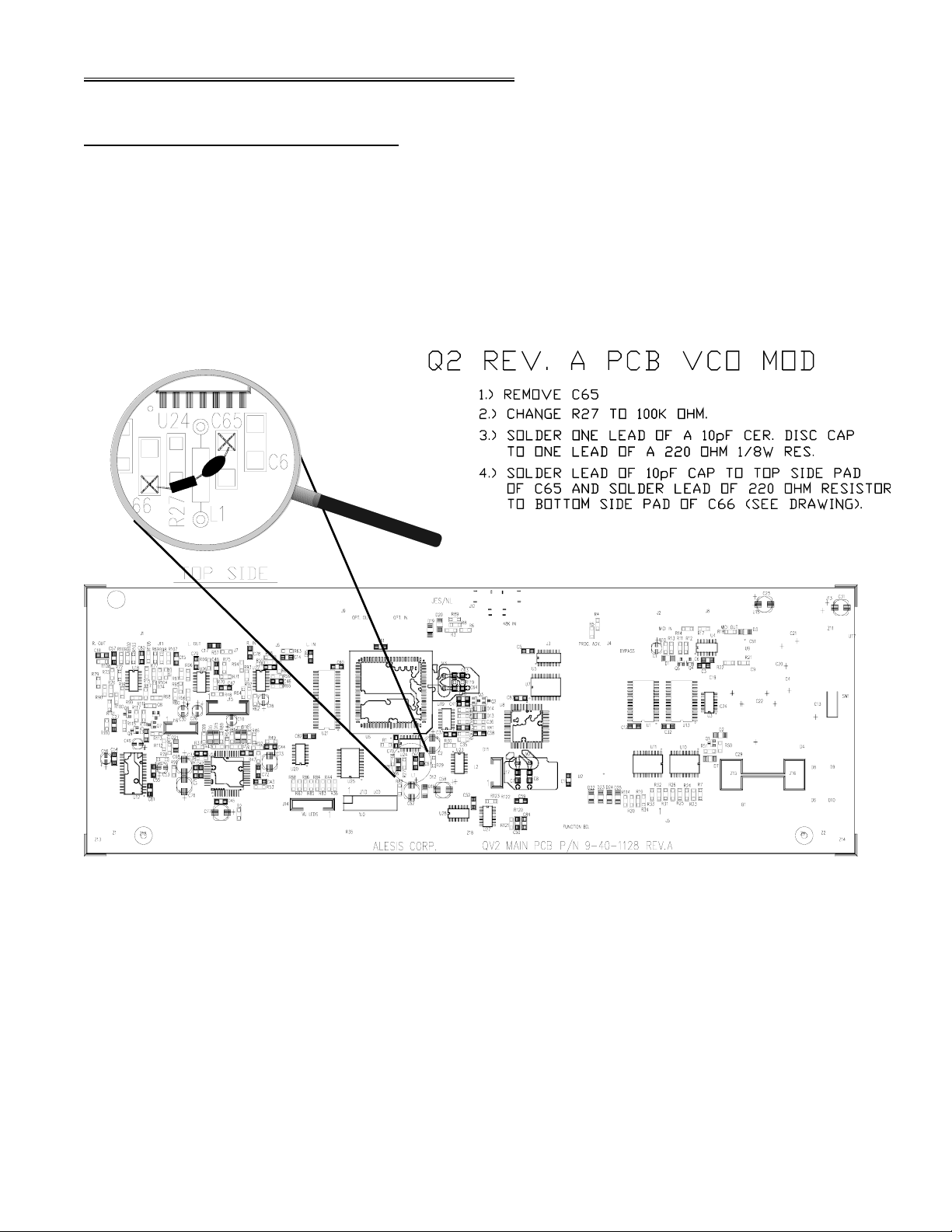
6.11 VCO Mod
The following changes (Diagrams 1 and 2) improve VCO (Voltage Controlled Oscillator)
performance, and prevents the unit from possibly detuning by itself.
Diagram 1
Alesis QuadraVerb II 2.00 A-1 07/19/06
Page 15
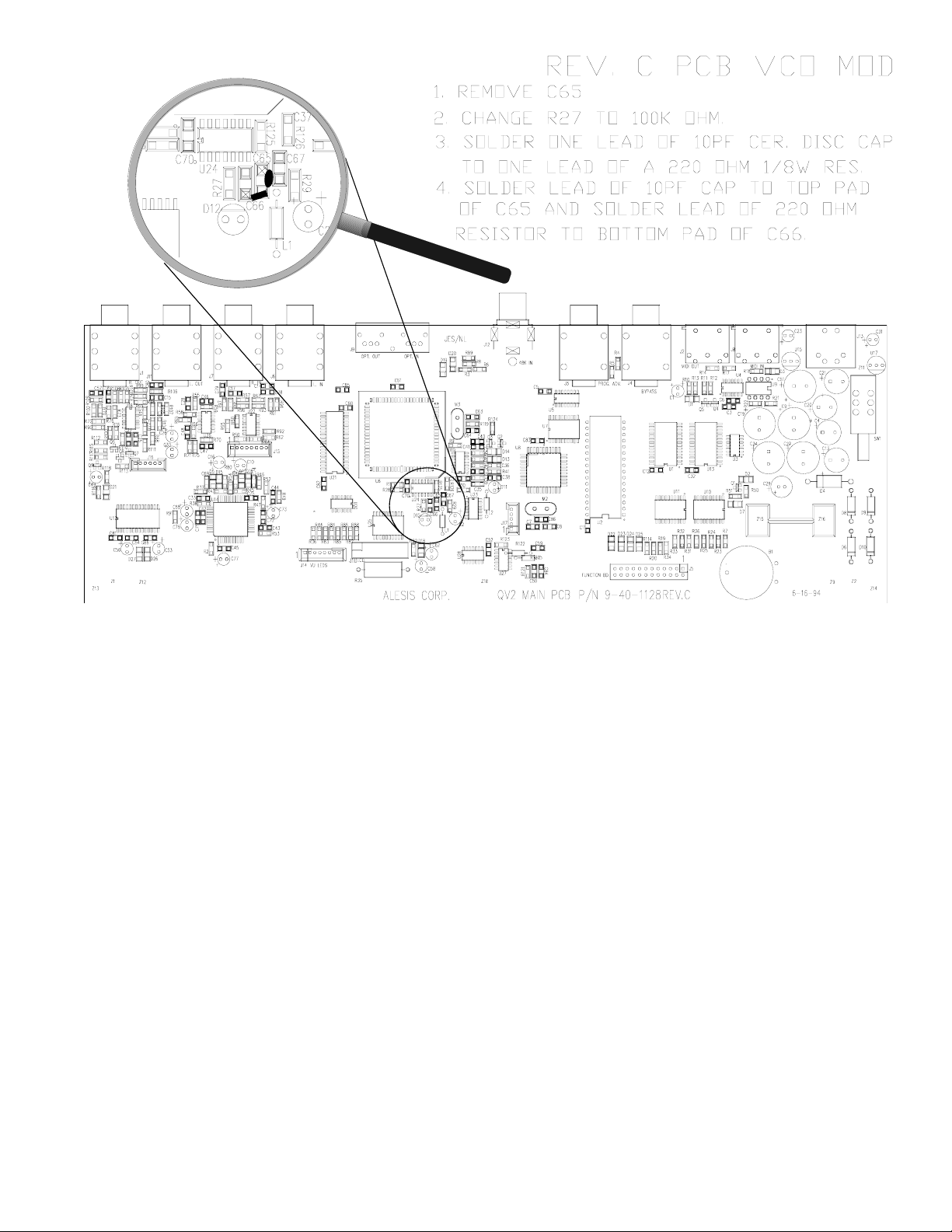
Diagram 2
6.12 SRAM Current Increase
R50 was changed from 100K to 10K. R51 was changed from 100K to 4.7K. These changes
ensure that the SRAM gets enough current to holds it's memory by making Q1 switch faster.
6.13 Main PCB change.
The Q2 Main PCB has changed from Revision A to Revision C. The new board offers
improved performance and incorporates several earlier changes.
6.14 Reset Circuit Change
The following three pages reflect changes made to the Q2 reset circuit. These changes
must be made to all Revision A and C Main PC Boards in order to maintain data integrity. The
first page applies to both Revision A and C PCBs, while sheet 2 applies to Revision A only, and
sheet 3 applies to Revision C only.
Alesis QuadraVerb II 2.00 A-2 07/19/06
Page 16

Alesis QuadraVerb II 2.00 A-3 07/19/06
Page 17

Alesis QuadraVerb II 2.00 A-4 07/19/06
Page 18

Alesis QuadraVerb II 2.00 A-5 07/19/06
Page 19
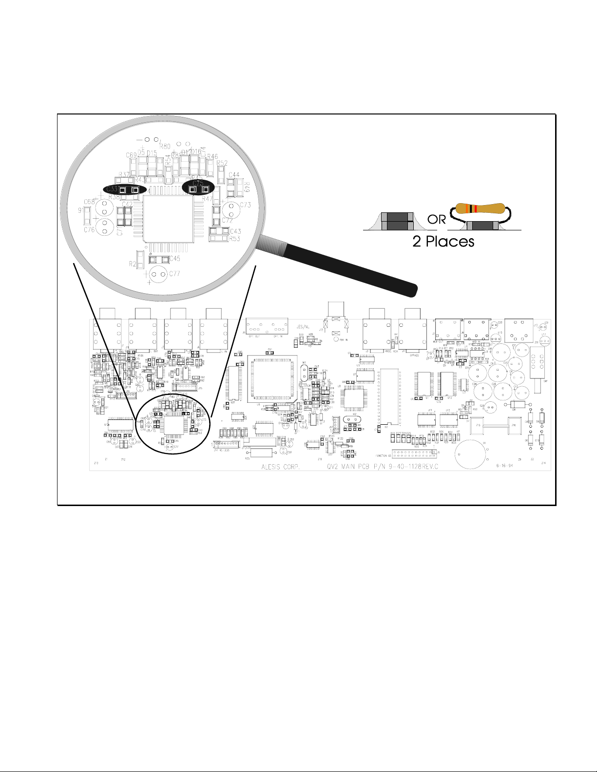
6.15 Revision A & C Input Changes
Add 2 3K resistors (AlPartNo.s 0-10-0302 {Surface Mount} or 0-00-0302 {Through Hole})
across capacitors C33 and C75 (See diagram 6 for locations). This change prevents the audio
outputs from inverting when the unit is clipping, reducing noise under these conditions.
Diagram 6
Alesis QuadraVerb II 2.00 A-6 07/19/06
Page 20
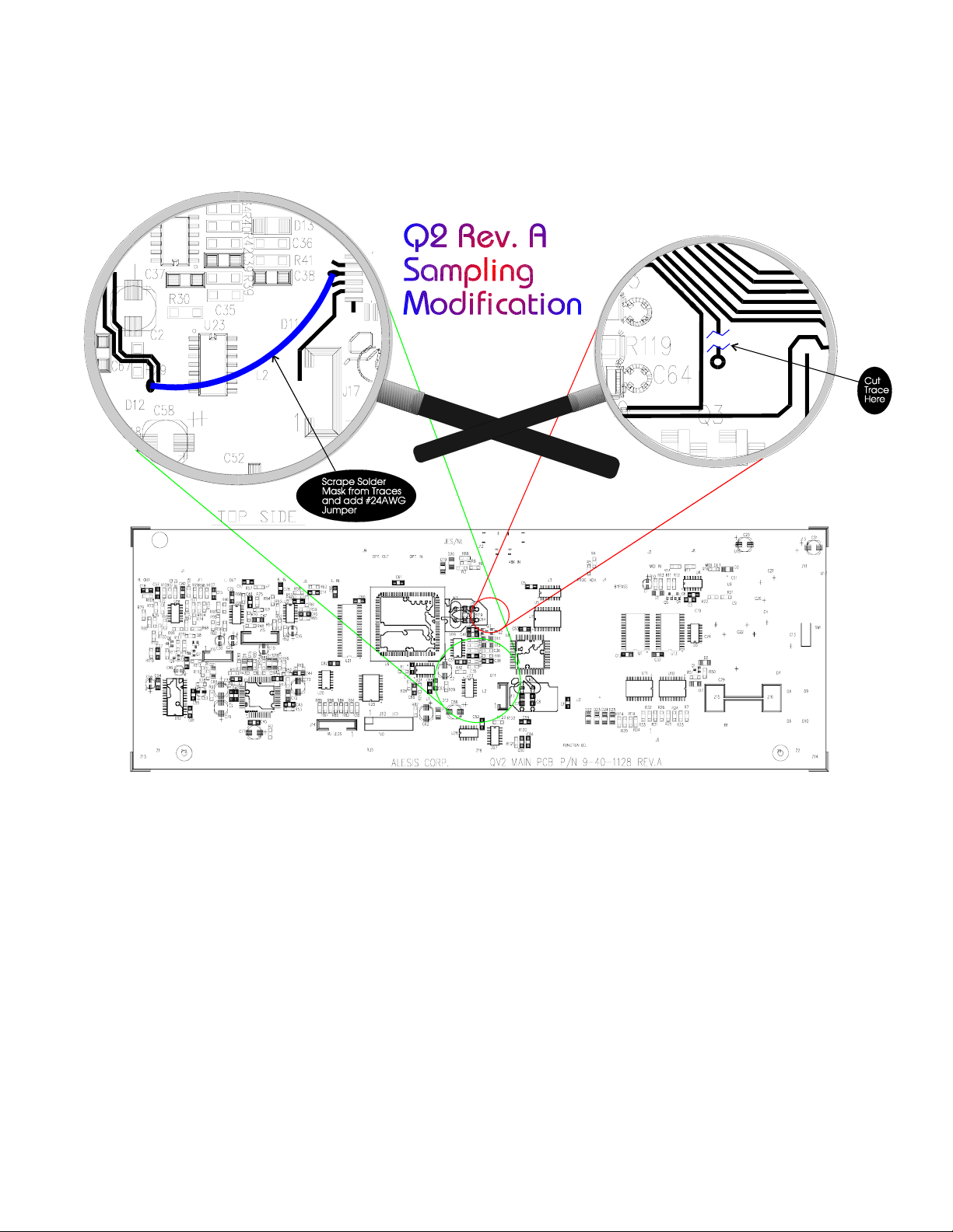
6.16 Revision A. Sampling Modification
To take advantage of the sampling feature included in software version 2.00 or higher it will
be necessary modify Revision A PCBs. The details of the modification are shown in Diagram 7. If
this modification is not performed when upgrading the software will display "UNIT NEEDS
SAMPLING UPGRADE" any time the sampling configuration is called up.
Diagram 7
Alesis QuadraVerb II 2.00 A-7 07/19/06
Page 21
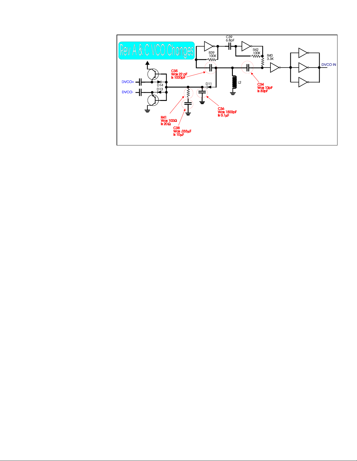
6.17 Revision A & C VCO Changes
This update
eliminates clock jitter that
can cause some
"crackling" sounds when
using digital I/O. Note
that this modification can
only work on units that
have software version
2.01 or higher, and thus
should only performed on
older units if there is a
specific complaint of Dig
I/O noise.
Diagram 8
Alesis QuadraVerb II 2.00 A-8 07/19/06
Page 22

7.00 Appendix 2 Test Procedures
If possible, user data should be saved (a DataDisk is recommended) prior to any servicing.
This, of course, may not always be possible (i.e. dead power supply, bad reset signal, corrupt
data, etc.). Saving user data may also be accomplished after unit functionality is restored (i.e.
power supply, or reset line, is repaired), and prior to further servicing, and testing. The unit should
always be reinitialized (power unit up while holding "PROGRAM", "COMPARE", and "←BLOCK "
buttons down) after changing the EPROM, SRAM, or any part of the battery backup.
7.10 Self Test
The following Steps outline the use of the Q2's self test routines. To initiate the self test
hold "PROGRAM" and "BLOCK →" while powering the unit up. The unit will then proceed to test
the following:
$ LEDs-All front panel LEDs are lit sequentially and immediately proceeds to the next test.
$ SWITCHES -Pressing Individual front panel buttons toggles the LEDs for each button
("BLOCK ←", "BLOCK →", "PAGE ←", and "PAGE →" toggle the LED of the adjacent button.)
All LEDs are toggled if "VALUE/ENTER" is pressed. Holding the buttons down causes the
LEDs to flash. Press "PROGRAM" and "BLOCK →" simultaneously to exit to the next test.
$ CUSTOM CHARACTERS (All)-Displays all custom LCD segments simultaneously. Press
"PROGRAM" and "BLOCK →" simultaneously to exit to the next test.
$ CUSTOM CHARACTERS (Single)-Use the "VALUE/ENTER" wheel to select individual custom
LCD characters. Press "PROGRAM" and "BLOCK →" simultaneously to exit to the next test.
$ ROM CKSUM-Checks the ROM's checksum for accuracy. Press "PROGRAM" and
"BLOCK →" simultaneously to exit the test routines.
7.20 Further Testing
7.21 Audio
Using a clean audio source (CD or DAT preferred) set up the Q2 according to the user
manual. Listen to the output of the Q2 for any distortion or unusual clicks and pops.
7.22 Digital I/O
The digital fiber optic input can be tested by connecting an optical cable from the optical
input of the Q2 to the output of any compatible unit (such as ADAT or QuadraSynth), and turning
on the Q2's "DIGITAL INPUT" (in the "GLOBAL" functions). Audio output should sound clean and
undistorted.
Similarly, the digital output can tested with either a digital or audio input using a unit that is
compatible (such as ADAT).
7.23 MIDI
MIDI is easily tested with a system exclusive storage unit (such as DataDisk or MIDI
equipped computer) by sending all programs to, and receiving them back from the storage unit.
Keyboard controllers, and patch changers also be used to test MIDI in.
Alesis QuadraVerb II 2.00 B-1 07/19/06
Page 23

8.00 Appendix 3 Helpful Hints & Common Solutions
Troubleshooting a complex device, such as the QuadraVerb II, can range from the
simplicity of looking, seeing, and reseating a loose cable, to examining complex timing
relationships of data and control, and replacing the "slightly" bad latch. The following table is
presented in an effort to relieve the beleaguered technician from having to "discover" some of the
common fixes we have seen. Please note that we only cover the most likely causes, not all of
them.
SYMPTOM POSSIBLE CAUSE SOLUTION
Unit is Dead (No lights, no
function).
Faulty digital (+5V) power
No LCD. Loose LCD cable. Check LCD cable and retest.
Faulty LCD cable. Replace and retest.
Faulty RESET signal. Troubleshoot and repair as
Faulty LCD. Replace and retest.
Software parameters out of
Distortion. Faulty Power analog (+12V, -
Faulty DAC (U12). Replace and retest.
Software parameters out of
Faulty PUP circuit. Troubleshoot and repair as
Faulty RESET signal. Troubleshoot and repair as
No MIDI in. Faulty opto-isolator (U9). Replace and retest.
No MIDI out. Hex inverter (U4) is faulty. Replace and retest.
No digital I/O. Faulty F/X ASIC (U6) Replace and retest.
No 48K in. Faulty F/X ASIC (U6) Replace and retest.
Faulty A.C. adapter. Replace and retest.
Troubleshoot and repair as
supply.
range.
12V) supply.
range.
necessary (see section 2.00
for details)
necessary (see section 5.11
for details)
Reinitialize unit and retest.
Troubleshoot and repair as
necessary (see section 2.00
for details)
Reinitialize unit and retest.
necessary (see section 2.10
for details)
necessary (see section 5.11
for details)
Alesis QuadraVerb II 2.00 C-1 07/19/06
Page 24

9.00 Appendix 4 Software History
DATE VERSION COMMENTS
07/26/94 1.00 Checksum: F3AAH. Initial software release.
07/26/94 1.01 Checksum: F6D5H.
1. Changed the names of a couple presets.
08/04/94 1.02 Checksum: 8896H.
1. Block move has been extended to include modulations.
2. The default footswitch range is now 0 Preset to 99 User.
3. The FX are updated when in ROUTE & COMPARE.
4. VUs reflect digital input selections and are turned off when the channel
is 3 through 8.
5. A stack overflow was fixed which happened when using processor
effects and editing a reverb decay parameter.
6. MIDI sysex receive ON/OFF works.
7. Changing modulation parameters no longer affect parameters on the
same page.
8. MIDI controller 0 can be used for program bank select when the table
is off (0 = Preset, 1 to 127 = User).
9. MIDI mods will no longer affect the program table and the program
table will no longer affect MIDI mods.
10. Defaults are added to the envelope and peak followers in blank
programs upon user memory clear.
11. PROGRAM switch goes to program page 1 if in page 2.
12. Program title now displays “User” or ”Preset”.
13. Data from the ADC is in 18 bit mode.
08/24/94 1.03 Checksum: 3ED2H.
1. The preset programs were changed
10/28/94 1.05 Checksum: 6ADDH.
1. Hold time was added to the ENVELOPE local generator.
2. The RAMP local generator was added.
3. Tap tempo delays are set by to MIDI clock.
4. Programs load 2x faster.
5. A program write protect was added under the Store pages.
6. VU meters no longer freeze when using external 48kHz clock.
7. MIDI sysex bugs were fixed.
8. Test routines for MIDI, optical I/O, and sram were added.
9. Reverb gate not affected by changing other parameters.
10. Modulation of parameters is more time consistent.
11. Modulation of Leslie speed is smoother.
12. Error message displayed when “MEMORY FULL” is caused by a
delay note value change.
13. Program change to a program containing a Leslie will not cause
occasional audio glitches.
07/06/95 2.00 Checksum: 9BFDH.
Alesis QuadraVerb II 2.00 D-1 07/19/06
Page 25

1. Added features are:
- Sampling
- Phase Inversion
- Triggered Panning
- Triggered Mono/Stereo Flanging
- Soft/Hard Overdrive
- Block Copy/Paste
- Advance and Bypass pedals as local modulation generators
- 100 more user programs
- Negative flanger feedback
- Block Bypass
- Improved Stereo Leslie with Linear/Circular mode
- Quick routing when a block is added
- LFO local modulation generator
- “DIG” indicator flashes when digital input not valid
2. The MIDI sysex additions are:
- In MIDI EDIT, Block Type can be edited
- The MIDI Global Dump accommodates the
larger footswitch range
- An “ENTER” command
- User Bank 1 dump and dump request
- Block Bypass dump and dump request
- MIDI program table dump and dump request
10/23/95 2.01 Checksum: D9ABH.
1. The test constraints to determine if the sampling hardware mod is
working have been loosened. This corrects the hardware problem
that is causing “SAMPLE HARDWARE UPDATE NEEDED”
error messages, allowing units allowing units with the VCO chip
mod to sample; pre-VCO chip units still work.
2. The test for the sampling hardware mod has been added to the self
test routines.
3. The footswitch local generator won’t retain modulation after
power-down.
4. If adding “quick” routes causes a “DSP FULL” message the
display is updated immediately to not show the routes.
5. On power-up the FX RAM (DRAM) is completely cleared so
quick power cycles won’t cause stuttering audio remnants to play.
6. The program bank selection by controller 0 is fixed.
7. The spelling of “ATTACK TIME” in the footswitch mod. pages is
corrected.
8. Transmitting MIDI to the Q2 during power-up will no longer
cause problems.
Alesis QuadraVerb II 2.00 D-2 07/19/06
Page 26

10.00 Appendix 5 MIDI Implementation
10.10 V1.0X
V1.0X September 9, 1994
SYSTEM EXCLUSIVE FORMAT
The QuadraVerb II MIDI System Exclusive message format is as follows:
F0 System exclusive status
00 00 0E Alesis manufacturer id#
0F QuadraVerb id#
cc Opcode
dd Data
: :
: :
F7 End-Of-Exclusive
OPCODES:
01 - MIDI Edit F0 00 00 0E 0F 01<function#> <block#> <page#> <parameter#> <data
16> F7
<function#> = 0= PARAMETER, 1= MIX, 2= GLOBAL
<block#> = (1-8) # of block to be edited. Doesn’t matter for GLOBAL edits.
<page#> = (1-#of last page under function) page # for value to be edited.
<parameter#> = (1-#of last parameter on page) parameter # of value
<data 16> is in format described below. It is a 16-bit value, which is transmitted in three
MIDI bytes, LSB first.
TWO QUADRAVERB II BYTES:
0: A7 A6 A5 A4 A3 A2 A1 A0 (LSB)
1: B7 B6 B5 B4 B3 B2 B1 B0 (MSB)
TRANSMITTED AS:
0: 0 A7 A6 A5 A4 A3 A2 A1
1: 0 A0 B7 B6 B5 B4 B3 B2
2: 0 B1 B0 0 0 0 0 0
02 - MIDI User Program Dump F0 00 00 0E 0E 02 <prog.#> <data> F7
<program#>= 0..99 selects individual user programs, 100 selects edit
<data> is in a packed format in order to optimize data transfer. Eight MIDI bytes are used to
transmit each block of 7 QuadraVerb II data bytes. If the 7 data bytes are looked at as one
56-bit word, the format for transmission is eight 7-bit words beginning with the most
significant bit of the first byte, as follows:
Alesis QuadraVerb II 2.00 E-1 07/19/06
Page 27

SEVEN QUADRAVERB II BYTES:
0: A7 A6 A5 A4 A3 A2 A1 A0
1: B7 B6 B5 B4 B3 B2 B1 B0
2: C7 C6 C5 C4 C3 C2 C1 C0
3: D7 D6 D5 D4 D3 D2 D1 D0
4: E7 E6 E5 E4 E3 E2 E1 E0
5: F7 F6 F5 F4 F3 F2 F1 F0
6: G7 G6 G5 G4 G3 G2 G1 G0
TRANSMITTED AS:
0: 0 A6 A5 A4 A3 A2 A1 A0
1: 0 B5 B4 B3 B2 B1 B0 A7
2: 0 C4 C3 C2 C1 C0 B7 B6
3: 0 D3 D2 D1 D0 C7 C6 C5
4: 0 E2 E1 E0 D7 D6 D5 D4
5: 0 F1 F0 E7 E6 E5 E4 E3
6: 0 G0 F7 F6 F5 F4 F3 F2
7: 0 G7 G6 G5 G4 G3 G2 G1
There are 306 data bytes sent for a single program dump, which corresponds to 256 bytes
of program data. With the header, the total number of bytes transmitted with a program
dump is 314. The location of each parameter within a program dump is shown in the next
section: QuadraVerb II Program Data Format.
03 - MIDI User Program Dump Request F0 00 00 0E 0F 03 <program#> F7
<program#>= 0..99 selects individual user programs, 100 selects current edit,
101 is a dump all request in which all user programs are dumped
as individual program dumps (02) followed by a global dump (07)
When received, the QuadraVerb II will respond to this message with a MIDI user program
dump (02) of the program number selected.
07 - MIDI Global Data Dump F0 00 00 0E 0F 07 <data> F7
<data> is in the same format as described in 00, but with a different number of bytes due to
the difference in the global parameter size. The total number of data bytes sent for a global
data dump is 16, which corresponds to 14 bytes of global data.
08 - MIDI Global Data Dump Request F0 00 00 0E 0F 08 F7
When received, the QuadraVerb II will respond to this message with a MIDI global data
dump (07).
09 - MIDI Bypass or Compare F0 00 00 0E 0F 09 <function> <off/on> F7
<function> = 0= BYPASS, 1= COMPARE
<off/on> = 0= function off, 1= function on
When received, the QuadraVerb II will respond to this message by turning
BYPASS/COMPARE OFF/ON.
Alesis QuadraVerb II 2.00 E-2 07/19/06
Page 28

0A - MIDI DSP Error Message F0 00 00 0E 0F 0A <data> F7
<data> = 1= “EFFECT MEMORY IS FULL”
2= “OUT OF LFOs”
4= “DSP IS FULL”
8= “BLOCK COMBINATION NOT ALLOWED”
PARAMETER FORMAT
The following specific parameter information shows the locations in which each parameter
resides after unpacking the data from its 7 bit MIDI format into the 8 bit format as described in opcode
00, program data dump.
GLOBAL DATA FORMAT
The Global parameters are comprised of 14 bytes of data. Unlike the Program, the Global parameters are
not packed so that each parameter occupies its own byte. This results in unused bits for most global bytes.
These bits must remain at 0. For direct parameter editing (sysex command 01H), the Page# and Parameter# are
given in the table below. The Function# should be set to 2 (=Global), and the Block# should be 1-8.
# Parameter name Page Parm lo lim hi lim bits bit address
0. LCD contrast 1 1 1 10 8 0:7-0:0
1. Footswitch range head 2 1 0 199 8 1:7-1:0
2. Footswitch range tail 2 2 0 199 8 2:7-2:0
3. VU meter peak hold 3 1 0 1 8 3:7-3:0
4. Input audio source 4 1 0 1 8 4:7-4:0
5. Sample clock source 5 1 0 1 8 5:7-5:0
6. Digital left input channel 6 2 1 8 8 6:7-6:0
7. Digital right input channel 6 3 1 8 8 7:7-7:0
8. Digital left output channel 6 4 1 8 8 8:7-8:0
9. Digital right output channel 6 1 1 8 8 9:7-9:0
10. Digital output mode 7 1 0 1 8 10:7-10:0
11. Tap tempo footswitch 8 1 0 2 8 11:7-11:0
12. Global direct signal 9 1 0 1 8 12:7-12:0
13. Reserved for future use (set to 0) 9 1 0 1 8 13:7-13:0
QUADRAVERB II PROGRAM DATA FORMAT
Programs contain 256 bytes of packed parameter data. The first 92 bytes are common
parameters for all programs. The next 164 bytes depend on the number of bytes required for
parameters of the effect blocks and the number of routes enabled. Usually, not all of these bytes are
used, and in this case the end of the routing is designated by 0FFH, 0FFH. Only numbers with
negative offsets are in 2’s complement form.
# Parameter name lo lim hi lim bits byte:msb-byte:lsb
PROGRAM NAME:
0. Program name ASCII digit 0 32 127 8 0:7-0:0
1. Program name ASCII digit 1 32 127 8 1:7-1:0
...
Alesis QuadraVerb II 2.00 E-3 07/19/06
Page 29

13. Program name ASCII digit 13 32 127 8 13:7-13:0
BLOCK TYPES:
14a. Block 1 type definition 0 4 * 3 14:7-14:5
14b. Block 1 subtype definition 0 ** 5 14:4-14:0
15a. Block 2 type definition 0 4 * 3 15:7-15:5
...
20b. Block 7 subtype definition 0 ** 5 20:4-20:0
21a. Block 8 type definition 0 4 * 3 21:7-21:5
21b. Block 8 subtype definition 0 ** 5 21:4-21:0
* Block type definitions are given in the next section: Block type definitions
** The upper limit and definition for the block subtype depend on the block type. The upper limit and
definition for the subtype are given in the section: Block subtype defintions
MODULATION:
22. Mod. 1 source 0 129 * 8 22:7-22:0
23. Mod. 1 target block # 1 11 ** 8 23:7-23:0
24a. Mod. 1 target type: parameter, route, or mix 0 2 *** 2 24:7-24:6
24b. Mod. 1 target # 0 *** 6 24:5-24:0
25. Mod. 1 amplitude -99 +99 8 25:7-25:0
26. Mod. 2 source 0 129 * 8 26:7-26:0
...
49. Mod. 7 amplitude -99 +99 8 49:7-49:0
50. Mod. 8 source 0 129 * 8 50:7-50:0
51. Mod. 8 target block # 1 11 ** 8 51:7-51:0
52a. Mod. 8 target type: parameter, route, or mix 0 2 *** 2 52:7-52:6
52b. Mod. 8 target # 0 *** 6 52:5-52:0
53. Mod. 8 amplitude -99 +99 8 53:7-53:0
* Definitions of the modulation sources are in the section: Modulation source definitions
** Target block # definition: 1 = block 1, ..., 8 = block 8, 9 = left out, 10 = right out, 11 = mix
parameters.
*** Definitions of the modulation targets are in the section: Modulation target definitions
Alesis QuadraVerb II 2.00 E-4 07/19/06
Page 30

BLOCK MIXES:
54. Direct level 0 100 8 54:7-54:0
55. Block 1 level 0 100 8 55:7-55:0
56. Block 1 inmix level 0 100 8 56:7-56:0
57. Block 2 level 0 100 8 57:7-57:0
...
68. Block 7 inmix level 0 100 8 68:7-68:0
69. Block 8 level 0 100 8 69:7-69:0
70. Block 8 inmix level 0 100 8 70:7-70:0
71. Master effects level 0 100 8 71:7-71:0
LOCAL GENERATORS:
72. Generator 1 type 0 1 * 8 72:7-72:0
73. Generator 1 trigger source channel 0 2 ** 8 73:7-73:0
74. Generator 1 attack threshold -32 0 8 74:7-74:0
75. Generator 1 release threshold -48 0 8 75:7-75:0
76. Generator 1 attack time 0 250 *** 8 76:7-76:0
77. Generator 1 release or decay time 0 250 *** 8 77:7-77:0
78. Generator 1 input gain 0 99 8 78:7-78:0
79. Reserved for future use (set to 0) 8 79:7-79:0
80. Reserved for future use (set to 0) 8 80:7-80:0
81. Reserved for future use (set to 0) 8 81:7-81:0
82. Generator 2 type 0 1 * 8 82:7-82:0
83. Generator 2 trigger source channel 0 2 ** 8 83:7-83:0
84. Generator 2 attack threshold -32 0 8 84:7-84:0
85. Generator 2 release threshold -48 0 8 85:7-85:0
86. Generator 2 attack time 0 250 *** 8 86:7-86:0
87. Generator 2 release or decay time 0 250 *** 8 87:7-87:0
88. Generator 2 input gain 0 99 8 88:7-88:0
89. Reserved for future use (set to 0) 8 89:7-89:0
90. Reserved for future use (set to 0) 8 90:7-90:0
91. Reserved for future use (set to 0) 8 91:7-91:0
* Generator type: 0 = Envelope generator, 1 = Peak follower
** Trigger source channel: 0 = Left channel, 1 = Right channel, 2 = Left & Right channels
*** This number is multiplied by 0.04 to get the decay in seconds.
BLOCK PARAMETERS
92. Parameter #1 for 1st defined block* (MSB) ** ** ** **
93. Parameter #1 for 1st defined block* (LSB) *** ** ** ** **
94. Parameter #2 for 1st defined block* (MSB) ** ** ** **
...
* Block parameters are not stored for blocks that are off. Parameters are stored in order of appearance on the
Quadraverb II display - by block #, parameter page #, and from left to right within the page; the 1st stored
parameter appears on the display at the left most block that is not off, on it’s 1st parameter page, at the left.
** The parameter definitions are given for each block type and subtype in the section: Block parameter
definitions
*** Exists only if the block parameter requires two bytes.
BLOCK ROUTING
92* Route #1 position byte (LSB) 0 255 ** 8 92*:7-92*:0
Alesis QuadraVerb II 2.00 E-5 07/19/06
Page 31

93* Route #1 position byte (MSB) 0 1 ** 1 93*:7-93*:7
93* Route #1 level 0 58 *** 7 93*:6-93*:0
94* Route #2 position byte (LSB) 0 255 ** 8 94*:7-94*:0
...
* This number is offset by the number of block parameter bytes that are stored.
** An equation for calculating the route position byte is given in the section: Route position definitions
*** This number has a corresponding dB level given by the table in the section: Route level definitions
BLOCK TYPE DEFINITIONS
This table defines the block types for a given parameter:
Parameter: Block type:
0 OFF
1 EQ
2 PCH
3 DLY
4 RVB
BLOCK SUBTYPE DEFINITIONS
These tables define the block subtypes for a given parameter. Different block subtype tables are
defined for each block type.
Type = EQ
Parameter: Block subtype
0 Lowpass filter
1 Bandpass filter
2 Highpass filter
3 Lowpass shelf eq
4 1 Band low parametric
5 1 Band high parametric
6 Highpass shelf eq
7 2 Band sweep shelf eq
8 3 Band parametric eq
9 4 Band parametric eq
10 5 Band graphic eq
11 Resonator
12 Mono tremolo
13 Stereo tremolo
14 Stereo simulator
Alesis QuadraVerb II 2.00 E-6 07/19/06
Page 32

Type = PCH
Type = DLY
Type = RVB
Parameter: Block subtype
0 Mono chorus
1 Stereo chorus
2 Quad chorus
3 Mono flanging
4 Stereo flanging
5 Phasor
6 Mono lezlie
7 Stereo lezlie
8 Pitch shifter
9 Pitch detune
10 Ring modulator
Parameter: Block subtype
0 Mono delay
1 Stereo delay
2 Ping pong delay
3 Multi tap delay
4 Tap tempo mono delay
5 Tap tempo ping pong dela
Parameter: Block subtype
0 Mono room
1 Room 1
2 Hall 1
3 Plate 1
4 Chamber 1
5 Room 2
6 Hall 2
7 Plate 2
8 Chamber 2
9 Large plate
10 Large room
11 Spring
12 Nonlinear
13 Reverse
Alesis QuadraVerb II 2.00 E-7 07/19/06
Page 33

MODULATION SOURCE DEFINITIONS
t
Parameter: Block subtype
0 Pitch bend
1 After touch
2 Note number
3 Note velocity
4 Controller 000
... ...
127 Controller 123
128 Local generator 1
129 Local generator 2
MODULATION TARGET DEFINITIONS
The modulation target type and target # make up an 8 bit word: TTNNNNNN (where TT denotes the
target type and NNNNNN denotes the target #). The targets are for the effect block or mix specified
by the target block #.
TT Modulation target type
00 Block parameter
01 Route level
10 Mix level
If TT = 00
NNNNNN Modulation target parame
0 Parameter #1
1 Parameter #2
... ...
32 Parameter #33
If TT = 01
NNNNNN Modulation target route
0 In left
1 In right
2 Block 1 inmix
3 Block 1 mix
4 Block 1 left
5 Block 1 right
6 Block 2 inmix
... ...
33 Block 8 right
Alesis QuadraVerb II 2.00 E-8 07/19/06
Page 34

If TT = 10
NNNNNN Modulation target mix
0 Direct level
1 Block 1 out level
2 Block 1 inmix level
3 Block 2 out level
4 Block 2 inmix level
... ...
16 Block 8 inmix level
17 Master fx level
BLOCK PARAMETER DEFINITIONS
These parameters are packed as 8 or 16 bit words MSB first in programs, but are always
considered 16 bit words LSB first in parameter edits.
EQ:
Parameter Page ParamBytes Low limit Hi limit Step
LOWPASS FILTER: type = 1, subtype = 0
lowpass fc 1 1 2 20 10,000 10
BANDPASS FILTER: type = 1, subtype = 1
bandpass fc 1 1 2 20 4,000 10
bw 1 2 1 20 200 1
HIGHPASS FILTER: type = 1, subtype = 2
highpass fc 1 1 2 200 20,000 10
LOWPASS SHELF EQ: type = 001, subtype = 3
lowpass 1 1 2 20 10,000 10
gain 1 2 2 -140 +140 1
1 BAND LOW PARAMETRIC: type = 1, subtype = 4
bandpass 1 1 2 20 2,000 10
gain 1 2 2 -140 +140 1
oct 1 3 1 20 200 1
1 BAND HIGH PARAMETRIC: type = 1, subtype = 5
bp 1 1 2 1500 10,000 10
gain 1 2 2 -140 +140 1
oct 1 3 1 20 250 1
HIGHPASS SHELF EQ: type = 1, subtype = 6
highpass 1 1 2 100 20,000 10
gain 1 2 2 -140 +140 1
2 BAND SWEEP SHELF EQ: type = 1, subtype = 7
lowpass 1 1 2 20 10,000 10
gain 1 2 2 -140 +140 1
highpass 2 1 2 100 20,000 10
gain 2 2 2 -140 +140 1
3 BAND PARAMETRIC EQ: type = 1, subtype = 8
lowpass 1 1 2 20 10,000 10
gain 1 2 2 -140 +140 1
mid band 2 1 2 20 2,000 1
Alesis QuadraVerb II 2.00 E-9 07/19/06
Page 35

dB 2 2 2 -140 +140 1
oct 2 3 1 20 200 1
highpass 3 1 2 100 20,000 10
gain 3 2 2 -140 +140 1
4 BAND PARAMETRIC EQ: type = 1, subtype = 9
lowpass 1 1 2 20 10,000 10
gain 1 2 2 -140 +140 1
low mid 2 1 2 20 2,000 1
dB 2 2 2 -140 +140 1
oct 2 3 1 20 200 1
high mid 3 1 2 1500 10,000 10
dB 3 2 2 -140 +140 1
oct 3 3 1 20 250 1
highpass 4 1 2 100 20,000 10
gain 4 2 2 -140 +140 1
5 BAND GRAPHIC EQ: type = 1, subtype = 10
63Hz 1 1 1 -14 +14 1
250Hz 1 2 1 -14 +14 1
1KHz 1 3 1 -14 +14 1
4KHz 1 4 1 -14 +14 1
16kHz 1 5 1 -14 +14 1
RESONATOR: type = 1, subtype = 11
tuning 1 1 1 0 60 1
decay 1 2 1 0 99 1
MONO TREMOLO: type = 1, subtype = 12
speed 1 1 1 0 99 1
depth 1 2 1 0 99 1
shape 1 3 1 0 1 1
STEREO TREMOLO: type = 1, subtype = 13
speed 1 1 1 0 99 1
depth 1 2 1 0 99 1
shape 1 3 1 0 1 1
STEREO SIMULATOR: type = 1, subtype = 14
degrees 1 1 1 0 99 1
Alesis QuadraVerb II 2.00 E-10 07/19/06
Page 36

PCH:
Parameter Page ParamBytes Low limit Hi limit Step
MONO CHORUS: type = 2, subtype = 0
speed 1 1 1 0 99 1
depth 1 2 1 0 99 1
feedback 1 3 1 0 99 1
chorus predelay 2 1 1 0 100 1
STEREO CHORUS: type = 2, subtype = 1
speed 1 1 1 0 99 1
depth 1 2 1 0 99 1
feedback 1 3 1 0 99 1
predelay chr1 2 1 1 0 100 1
chr2 2 2 1 0 100 1
STEREO CHORUS: type = 2, subtype = 2
speed 1 1 1 0 99 1
depth 1 2 1 0 99 1
feedback 1 3 1 0 99 1
predelay chr1 2 1 1 0 100 1
chr2 2 2 1 0 100 1
predelay chr3 3 1 1 0 100 1
chr4 3 2 1 0 100 1
MONO FLANGING: type = 2, subtype = 3
speed 1 1 1 0 99 1
depth 1 2 1 0 99 1
feedback 1 3 1 0 99 1
flanging shape 2 1 1 0 1 1
STEREO FLANGING: type = 2, subtype = 4
speed 1 1 1 0 99 1
depth 1 2 1 0 99 1
feedback 1 3 1 0 99 1
flanging shape 2 1 1 0 1 1
PHASOR: type = 2, subtype = 5
phasor speed 1 1 1 0 99 1
depth 1 2 1 0 99 1
MONO LEZLIE: type = 2, subtype = 6
lezlie motor 1 1 1 0 1 1
speed 1 2 1 0 1 1
high rotor level 2 1 1 -12 +6 1
STEREO LEZLIE: type = 2, subtype = 7
lezlie motor 1 1 1 0 1 1
speed 1 2 1 0 1 1
high rotor level 2 1 1 -12 +6 1
stereo separation 3 1 1 0 99 1
PITCH SHIFTER: type = 2, subtype = 8
pitch shift fine 1 1 1 -99 +99 1
coarse 1 2 1 -12 +12 1
PITCH DETUNE: type = 2, subtype = 9
detune amount 1 1 1 -99 +99 1
Alesis QuadraVerb II 2.00 E-11 07/19/06
Page 37

DLY:
Parameter Page ParamBytes Low limit Hi limit Step
MONO DELAY: type = 3, subtype = 0
delay 1 1 2 1 50,000 1
note value 1 2 1 0 12 1
feedback 2 1 1 0 99 1
STEREO DELAY: type = 3, subtype = 1
L dly 1 1 2 1 50,000 1
note value 1 2 1 0 12 1
L feedback 2 1 1 0 99 1
R dly 3 1 2 1 50,000 1
note value 3 2 1 0 12 1
R feedback 4 1 1 0 99 1
PING PONG DELAY: type = 3, subtype = 2
delay 1 1 2 1 25,000 1
note value 1 2 1 0 12 1
feedback 2 1 1 0 99 1
MULTI TAP DELAY: type = 3, subtype = 3
delay 1 1 2 1 50,000 1
tap level 1 2 1 0 38 1
L<- ->R 1 3 1 1 99 1
fb 1 4 1 0 99 1
delay 2 1 2 1 50,000 1
tap level 2 2 1 0 38 1
L<- ->R 2 3 1 1 99 1
fb 2 4 1 0 99 1
delay 3 1 2 1 50,000 1
tap level 3 2 1 0 38 1
L<- ->R 3 3 1 1 99 1
fb 3 4 1 0 99 1
delay 4 1 2 1 50,000 1
tap level 4 2 1 0 38 1
L<- ->R 4 3 1 1 99 1
fb 4 4 1 0 99 1
delay 5 1 2 1 50,000 1
tap level 5 2 1 0 38 1
L<- ->R 5 3 1 1 99 1
fb 5 4 1 0 99 1
master feedback 6 1 1 0 99 1
TAP TEMPO MONO DELAY: type = 3, subtype = 4
delay 1 1 2 1 50,000 1
note value 1 2 1 0 38 1
feedback 2 1 1 0 99 1
TAP TEMPO PING PONG DELAY: type = 3, subtype = 5
delay 1 1 2 1 25,000 1
note value 1 2 1 0 38 1
feedback 2 1 1 0 99 1
Alesis QuadraVerb II 2.00 E-12 07/19/06
Page 38

RVB:
Parameter Page ParamBytes Low limit Hi limit Step
MONO ROOM: type = 4, subtype = 0
decay 1 1 1 0 99 1
damping hi 1 2 1 0 99 1
lo 1 3 1 0 99 1
reverb density 2 1 1 0 99 1
diffusion 2 2 1 0 99 1
input high freq roll off 3 1 2 200 20,000 50
predelay 4 1 1 1 250 1
mix direct<- ->dly 4 2 1 1 99 1
gate trig 5 1 1 0 2 1
gated level 5 2 1 0 99 1
gate hold 6 1 2 0 500 10
release 6 2 2 10 500 10
ROOM 1: type = 4, subtype = 1
decay 1 1 1 0 99 1
damping hi 1 2 1 0 99 1
lo 1 3 1 0 99 1
reverb density 2 1 1 0 99 1
diffusion 2 2 1 0 99 1
input high freq roll off 3 1 2 200 20,000 50
predelay 4 1 1 1 250 1
mix direct<- ->dly 4 2 1 1 99 1
gate trig 5 1 1 0 2 1
gated level 7 2 1 0 99 1
gate hold 5 2 2 0 500 10
release 6 1 2 10 500 10
HALL 1: type = 4, subtype = 2
decay 1 1 1 0 99 1
damping hi 1 2 1 0 99 1
lo 1 3 1 0 99 1
reverb density 2 1 1 0 99 1
diffusion 2 2 1 0 99 1
input high freq roll off 3 1 2 200 20,000 50
predelay 4 1 1 1 250 1
mix direct<- ->dly 4 2 1 1 99 1
gate trig 5 1 1 0 2 1
gated level 5 2 1 0 99 1
gate hold 6 1 2 0 500 10
release 6 2 2 10 500 10
ROOM 1: type = 4, subtype = 3
decay 1 1 1 0 99 1
damping hi 1 2 1 0 99 1
lo 1 3 1 0 99 1
reverb density 2 1 1 0 99 1
diffusion 2 2 1 0 99 1
input high freq roll off 3 1 2 200 20,000 50
Alesis QuadraVerb II 2.00 E-13 07/19/06
Page 39

predelay 4 1 1 1 250 1
mix direct<- ->dly 4 2 1 1 99 1
gate trig 5 1 1 0 2 1
gated level 5 2 1 0 99 1
gate hold 6 1 2 0 500 10
release 6 2 2 10 500 10
PLATE 1: type = 4, subtype = 4
decay 1 1 1 0 99 1
damping hi 1 2 1 0 99 1
lo 1 3 1 0 99 1
reverb density 2 1 1 0 99 1
diffusion 2 2 1 0 99 1
input high freq roll off 3 1 2 200 20,000 50
predelay 4 1 1 1 250 1
mix direct<- ->dly 4 2 1 1 99 1
gate trig 5 1 1 0 2 1
gated level 5 2 1 0 99 1
gate hold 6 1 2 0 500 10
release 6 2 2 10 500 10
CHAMBER 1: type = 4, subtype = 5
decay 1 1 1 0 99 1
damping hi 1 2 1 0 99 1
lo 1 3 1 0 99 1
reverb density 2 1 1 0 99 1
diffusion 2 2 1 0 99 1
input high freq roll off 3 1 2 200 20,000 50
predelay 4 1 1 1 250 1
mix direct<- ->dly 4 2 1 1 99 1
gate trig 5 1 1 0 2 1
gated level 5 2 1 0 99 1
gate hold 6 1 2 0 500 10
release 6 2 2 10 500 10
ROOM 2: type = 4, subtype = 6
decay 1 1 1 0 99 1
damping hi 1 2 1 0 99 1
lo 1 3 1 0 99 1
reverb density 2 1 1 0 99 1
diffusion 2 2 1 0 99 1
input high freq roll off 3 1 2 200 20,000 50
predelay 4 1 1 1 250 1
mix direct<- ->dly 4 2 1 1 99 1
reflection level 5 1 1 0 99 1
spread 5 2 1 0 99 1
reverberation swirl 6 1 1 0 99 1
gate trig 7 1 1 0 2 1
gated level 7 2 1 0 99 1
gate hold 8 1 2 0 500 10
release 8 2 2 10 500 10
Alesis QuadraVerb II 2.00 E-14 07/19/06
Page 40

HALL 2: type = 4, subtype = 7
decay 1 1 1 0 99 1
damping hi 1 2 1 0 99 1
lo 1 3 1 0 99 1
reverb density 2 1 1 0 99 1
diffusion 2 2 1 0 99 1
input high freq roll off 3 1 2 200 20,000 50
predelay 4 1 1 1 250 1
mix direct<- ->dly 4 2 1 1 99 1
reflection level 5 1 1 0 99 1
spread 5 2 1 0 99 1
reverberation swirl 6 1 1 0 99 1
gate trig 7 1 1 0 2 1
gated level 7 2 1 0 99 1
gate hold 8 1 2 0 500 10
release 8 2 2 10 500 10
PLATE 2: type = 4, subtype = 8
decay 1 1 1 0 99 1
damping hi 1 2 1 0 99 1
lo 1 3 1 0 99 1
reverb density 2 1 1 0 99 1
diffusion 2 2 1 0 99 1
input high freq roll off 3 1 2 200 20,000 50
predelay 4 1 1 1 250 1
mix direct<- ->dly 4 2 1 1 99 1
reflection level 5 1 1 0 99 1
spread 5 2 1 0 99 1
reverberation attack 6 1 1 0 99 1
gate trig 7 1 1 0 2 1
gated level 7 2 1 0 99 1
gated hold 8 1 2 0 500 10
release 8 2 2 10 500 10
CHAMBER 2: type = 4, subtype = 9
decay 1 1 1 0 99 1
damping hi 1 2 1 0 99 1
lo 1 3 1 0 99 1
reverb density 2 1 1 0 99 1
diffusion 2 2 1 0 99 1
input high freq roll off 3 1 2 200 20,000 50
predelay 4 1 1 1 250 1
mix direct<- ->dly 4 2 1 1 99 1
reflection level 5 1 1 0 99 1
spread 5 2 1 0 99 1
reverberation attack 6 1 1 0 99 1
gate trig 7 1 1 0 2 1
gated level 7 2 1 0 99 1
gate hold 8 1 2 0 500 10
release 8 2 2 10 500 10
Alesis QuadraVerb II 2.00 E-15 07/19/06
Page 41

LARGE PLATE: type = 4, subtype = 10
decay 1 1 1 0 99 1
damping hi 1 2 1 0 99 1
lo 1 3 1 0 99 1
reverb density 2 1 1 0 99 1
diffusion 2 2 1 0 99 1
input high freq roll off 3 1 2 200 20,000 50
predelay 4 1 1 1 250 1
mix direct<- ->dly 4 2 1 1 99 1
reflection level 5 1 1 0 99 1
spread 5 2 1 0 99 1
reverberation swirl 6 1 1 0 99 1
gate trig 7 1 1 0 2 1
gated level 7 2 1 0 99 1
gate hold 8 1 2 0 500 10
release 8 2 2 10 500 10
LARGE ROOM: type = 4, subtype = 11
decay 1 1 1 0 99 1
damping hi 1 2 1 0 99 1
lo 1 3 1 0 99 1
reverb density 2 1 1 0 99 1
diffusion 2 2 1 0 99 1
input high freq roll off 3 1 2 200 20,000 50
predelay 4 1 1 1 250 1
mix direct<- ->dly 4 2 1 1 99 1
reflection level 5 1 1 0 99 1
spread 5 2 1 0 99 1
reverberation swirl 6 1 1 0 99 1
gate trig 7 1 1 0 2 1
gate level 7 2 1 0 99 1
gate hold 8 1 2 0 500 10
release 8 2 2 10 500 10
SPRING: type = 4, subtype = 12
decay 1 1 1 0 99 1
damping hi 1 2 1 0 99 1
lo 1 3 1 0 99 1
reverb density 2 1 1 0 99 1
diffusion 2 2 1 0 99 1
input high freq roll off 3 1 2 200 20,000 50
predelay 4 1 1 1 250 1
mix direct<- ->dly 4 2 1 1 99 1
gate trig 5 1 1 0 2 1
gate level 5 2 1 0 99 1
gate hold 6 1 2 0 500 10
release 6 2 2 10 500 10
Alesis QuadraVerb II 2.00 E-16 07/19/06
Page 42

NONLINEAR: type = 4, subtype = 13
gate hold time 1 1 1 0 99 1
reverb density 2 1 1 0 99 1
diffusion 2 2 1 0 99 1
input high freq roll off 3 1 2 200 20,000 50
predelay 4 1 1 1 250 1
mix direct<- ->dly 4 2 1 1 99 1
ROUTE POSITION DEFINITIONS
Route position byte (9bits) = Sroute + [4*(Sblock-1)] + [34*(Dblock-1)]
where,
Sroute= route source #: 0= Input L, 1= Input R, 2= Block inmix, 3= Block mix, 4= Block L, 5= Block R
Sblock= route source block #: 1= Input, 1= Block 1, ..., 8= Block 8
Dblock= route destination block #: 1= Block 1, ..., 8= Block 8, 9= Out L, 10= Out R
ROUTE LEVEL DEFINITIONS
Below is a table that gives the corresponding dB level for a given route level #:
Rout level # Parameter dB
0 OFF
1 -48.0 dB
2 -42.0 dB
3 -38.0 dB
4 -36.0 dB
5 -34.0 dB
6 -32.0 dB
7 -31.0 dB
8 -30.0 dB
9 -29.0 dB
10 -28.0 dB
11 -27.0 dB
12 -26.0 dB
13 -25.0 dB
14 -24.0 dB
15 -23.0 dB
16 -22.0 dB
17 -21.0 dB
18 -20.0 dB
19 -19.5 dB
20 -19.0 dB
Alesis QuadraVerb II 2.00 E-17 07/19/06
Page 43

21 -18.5 dB
22 -18.0 dB
23 -17.5 dB
24 -17.0 dB
25 -16.5 dB
26 -16.0 dB
27 -15.5 dB
28 -15.0 dB
29 -14.5 dB
30 -14.0 dB
31 -13.5 dB
32 -13.0 dB
33 -12.5 dB
34 -12.0 dB
35 -11.5 dB
36 -11.0 dB
37 -10.5 dB
38 -10.0 dB
39 -9.5 dB
40 -9.0 dB
41 -8.5 dB
42 -8.0 dB
43 -7.5 dB
44 -7.0 dB
45 -6.5 dB
46 -6.0 dB
47 -5.5 dB
48 -5.0 dB
49 -4.5 dB
50 -4.0 dB
51 -3.5 dB
52 -3.0 dB
53 -2.5 dB
54 -2.0 dB
55 -1.5 dB
56 -1.0 dB
57 -0.5 dB
58 -0.0 dB
Alesis QuadraVerb II 2.00 E-18 07/19/06
Page 44

10.20 V2.0X
Version 2.0X 6/26/95
SYSTEM EXCLUSIVE FORMAT
The QuadraVerb 2 MIDI System Exclusive message format is as follows:
F0 System exclusive status
00 00 0E Alesis manufacturer id#
0F QuadraVerb id#
cc Opcode
dd Data
: :
: :
F7 End-Of-Exclusive
OPCODES:
01 - MIDI Edit F0 00 00 0E 0F 01 <function#> <block#> <page#>
<parameter#> <data> F7
<function#> = 0= PARAMETER, 1= MIX, 2= GLOBAL, 3= TYPE*
<block#> = (1-8) # of block to be edited. Doesn’t matter for GLOBAL edits.
<page#> = (1-#of last page under function) page # for value to be edited.
<parameter#> = (1-#of last parameter on page) parameter # of value
<data> is in format described below. It is a 16-bit value, which is transmitted in three MIDI
bytes, LSB first.
TWO QUADRAVERB 2 BYTES:
0: A7 A6 A5 A4 A3 A2 A1 A0 (LSB)
1: B7 B6 B5 B4 B3 B2 B1 B0 (MSB)
TRANSMITTED AS:
0: 0 A7 A6 A5 A4 A3 A2 A1
1: 0 A0 B7 B6 B5 B4 B3 B2
2: 0 B1 B0 0 0 0 0 0
* Editing of a flashing TYPE parameter should be followed by an ‘ENTER’ MIDI sysex message
(0B).
02 - MIDI User Program Dump
<program#>= 0..99 selects individual user bank 0 programs, 100 selects edit
<data> is in a packed format in order to optimize data transfer. Eight MIDI bytes are used to
transmit each block of 7 QuadraVerb 2 data bytes. If the 7 data bytes are looked at as one
56-bit word, the format for transmission is eight 7-bit words beginning with the most
significant bit of the first byte, as follows:
F0 00 00 0E 0E 02 <prog.#> <data> F7
Alesis QuadraVerb II 2.00 E-19 07/19/06
Page 45

SEVEN QUADRAVERB 2 BYTES:
0: A7 A6 A5 A4 A3 A2 A1 A0
1: B7 B6 B5 B4 B3 B2 B1 B0
2: C7 C6 C5 C4 C3 C2 C1 C0
3: D7 D6 D5 D4 D3 D2 D1 D0
4: E7 E6 E5 E4 E3 E2 E1 E0
5: F7 F6 F5 F4 F3 F2 F1 F0
6: G7 G6 G5 G4 G3 G2 G1 G0
TRANSMITTED AS:
0: 0 A6 A6 A5 A4 A3 A2 A1
1: 0 A0 B7 B6 B5 B4 B3 B2
2: 0 B1 B0 C7 C6 C5 C4 C3
3: 0 C2 C1 C0 D7 D6 D5 D4
4: 0 D3 D2 D1 D0 E7 E6 E5
5: 0 E4 E3 E2 E1 E0 F7 F6
6: 0 F5 F4 F3 F2 F1 F0 G7
7: 0 G6 G5 G4 G3 G2 G1 G0
There are 306 data bytes sent for a single program dump, which corresponds to 256 bytes
of program data. With the header, the total number of bytes transmitted with a program
dump is 314. The location of each parameter within a program dump is shown in the next
section: QuadraVerb 2 Program Data Format.
03 - MIDI User Bank 0 Program Dump Request F0 00 00 0E 0F 03 <program#> F7
<program#>= 0..99 selects individual user programs in User Bank 0, 100 selects
current edit, 101 is a dump all request
When received, the QuadraVerb 2 will respond to this message with a MIDI user program
dump (02) of the User Bank 0 program or edit selected.
For the dump all request User Bank 0 programs are dumped as individual program dumps
(02) followed by all User Bank 1 programs dumped as individual program dumps (0C), a
global parameter dump (07), and finally a MIDI program table dump (11).
07 - MIDI Global Data Dump F0 00 00 0E 0F 07 <data> F7
<data> is in the same MIDI data format as described in 02, but with a different number of
bytes due to the difference in the global parameter size.The global parameters for the MIDI
dump are packed into 14 Quadraverb 2 bytes (see below) and transferred as 16 MIDI bytes.
The last byte packs the most significant bit of the footswitch head parameter into bit address
13:0 and the msb of the footswitch tail into bit address 13:1. The following table outlines
this:
Alesis QuadraVerb II 2.00 E-20 07/19/06
Page 46

GLOBAL PARAMETER PACKING:
Parameter name lo lim hi lim bits bit address
LCD contrast 1 10 8 0:7-0:0
Footswitch range head LSB* 0 299 8 1:7-1:0
Footswitch range tail LSB* 0 299 8 2:7-3:0
VU meter peak hold 0 1 8 3:7-3:0
Input audio source 0 1 8 4:7-4:0
Sample clock source 0 1 8 5:7-5:0
Digital left input channel 1 8 8 6:7-6:0
Digital right input channel 1 8 8 7:7-7:0
Digital left output channel 1 8 8 8:7-8:0
Digital right output channel 1 8 8 9:7-9:0
Digital output mode 0 1 8 10:7-10:0
Tap tempo footswitch 0 2 8 11:7-11:0
Global direct signal 0 1 8 12:7-12:0
Footswitch range head MSB, tail MSB* 0 299 2 13:1-13:0
*The MSBs for the footswitch parameters are stored in bit address 13:1 and13:0.
Bits 13:7 through 13:2 should be set to 0.
08 - MIDI Global Data Dump Request F0 00 00 0E 0F 08 F7
When received, the QuadraVerb 2 will respond to this message with a MIDI global data
dump (07).
09 - MIDI Bypass or Compare F0 00 00 0E 0F 09 <function> <off/on> F7
<function> = 0= BYPASS, 1= COMPARE
<off/on> = 0= function off, 1= function on
When received, the QuadraVerb 2 will respond to this message by turning
BYPASS/COMPARE OFF/ON.
0A - MIDI DSP Error Message
<data> = 1= “EFFECT MEMORY IS FULL”
2= “OUT OF LFOs”
4= “DSP IS FULL”
8= “BLOCK COMBINATION NOT ALLOWED”
0B - MIDI Enter Message
This performs the ENTER function on the current parameter. It is useful for
acting on flashing parameters.
0C - MIDI User Bank 1 Program Dump F0 00 00 0E 0E 0C<prog.#> <data> F7
<program#>= 0..99 selects individual User Bank 1 programs, 100 selects edit
<data> is the same format as the <data> of the User Bank 0 Dump opcode (02)
F0 00 00 0E 0F 0A <data> F7
F0 00 00 0E 0F 0B F7
Alesis QuadraVerb II 2.00 E-21 07/19/06
Page 47

0D - MIDI User Bank 1 Program Dump Request F0 00 00 0E 0F 0D<program#>F7
<program#>= 0..99 selects individual user programs in User Bank 1, 100 selects
current edit, 101 is a dump all request
When received, the QuadraVerb 2 will respond to this message with a MIDI user program
dump (0C) of the User Bank 1 program or edit selected.
For the dump all request User Bank 0 programs are dumped as individual program dumps
(02) followed by all User Bank 1 programs dumped as individual program dumps (0C), a
global parameter dump (07), and finally a MIDI program table dump (11).
0F - MIDI Block Bypass Dump F0 00 00 0E 0F 0F <data> F7
<data> is in format described below. It is an 8-bit value, which is transmitted in two MIDI
bytes. Bit A7 corresponds to the block bypass of block #8, likewise,
A6 corresponds to block #7 ... and A0 corresponds to block#1. If thebit value= 1,
the block is bypassed; if thebit value= 0, the block is not bypassed.
ONE QUADRAVERB 2 BYTE:
0: A7 A6 A5 A4 A3 A2 A1 A0
TRANSMITTED AS:
0: 0 A7 A6 A5 A4 A3 A2 A1
1: 0 A0 0 0 0 0 0 0
10 - MIDI Block Bypass Dump Request F0 00 00 0E 0F 10 F7
When received, the QuadraVerb 2 will respond to this message with a MIDI Block Bypass
Dump (0F).
11 - MIDI Program Table Dump F0 00 00 0E 0F 11 <data> F7
<data> is in format described below. The 128 MIDI program table entries are
9-bits each, and are transmitted in two MIDI bytes. Values in the range 0-99 correspond to
Presets 0-99, values 100-199 correspond to User bank 0 programs 0-99, and values 200-
299 correspond to User bank 1 programs 0-99.
TWO QUADRAVERB 2 MIDI TABLE ENTRIES:
0: A7 A6 A5 A4 A3 A2 A1 A0
1: 0 0 0 0 0 0 0 A8
2: B7 B6 B5 B4 B3 B2 B1 B0
3: 0 0 0 0 0 0 0 B8
TRANSMITTED AS:
0: 0 A6 A5 A4 A3 A2 A1 A0
1: 0 0 0 0 0 0 A8 A7
2: 0 B6 B5 B4 B3 B2 B1 B0
3: 0 0 0 0 0 0 B8 B7
12 - MIDI Program Table DumpRequest F0 00 00 0E 0F 12 F7
Alesis QuadraVerb II 2.00 E-22 07/19/06
Page 48

When received, the QuadraVerb 2 will respond to this message with a MIDI Program Table
Dump (11).
PARAMETER FORMAT
The following specific parameter information shows the locations in which each parameter
resides after unpacking the data from its 7 bit MIDI format into the 8 bit format as described in opcode
02, program data dump.
GLOBAL DATA FORMAT
The Global parameters are comprised of 14 bytes of data. Unlike the Program, the Global parameters are
not packed. This results in unused bits for most global bytes. These bits must remain at 0. For direct parameter
editing (sysex command 01H), the Page# and Parameter# are given in the table below. The Function# should
be set to 2 (=Global), and the Block# should be 1-8.
# Parameter name Page Parm lo lim hi lim bits bit address
0. LCD contrast 1 1 1 10 8 0:7-0:0
1. Footswitch range head 2 1 0 299 16 2:7-1:0
2. Footswitch range tail 2 2 0 299 16 4:7-3:0
3. VU meter peak hold 3 1 0 1 8 5:7-5:0
4. Input audio source 4 1 0 1 8 6:7-6:0
5. Sample clock source 5 1 0 1 8 7:7-7:0
6. Digital left input channel 6 2 1 8 8 8:7-8:0
7. Digital right input channel 6 3 1 8 8 9:7-9:0
8. Digital left output channel 6 4 1 8 8 10:7-10:0
9. Digital right output channel 6 1 1 8 8 11:7-11:0
10. Digital output mode 7 1 0 1 8 12:7-12:0
11. Tap tempo footswitch 8 1 0 2 8 13:7-13:0
12. Global direct signal 9 1 0 1 8 14:7-14:0
QUADRAVERB 2 PROGRAM DATA FORMAT
Programs contain 256 bytes of packed parameter data. The first 92 bytes are common parameters
for all programs. The next 164 bytes depend on the number of bytes required for parameters of the
effect blocks and the number of routes enabled. Usually, not all of these bytes are used, and in this
case the end of the routing is designated by 0FFH, 0FFH. Only numbers with negative offsets are in
2’s complement form.
# Parameter name lo lim hi lim bits byte:msb-byte:lsb
PROGRAM NAME:
0. Program name ASCII digit 0 32 127 8 0:7-0:0
...
13. Program name ASCII digit 13 32 127 8 13:7-13:0
Alesis QuadraVerb II 2.00 E-23 07/19/06
Page 49

BLOCK TYPES:
14a. Block 1 type definition 0 4 * 3 14:7-14:5
14b. Block 1 subtype definition 0 ** 5 14:4-14:0
15a. Block 2 type definition 0 4 * 3 15:7-15:5
...
20b. Block 7 subtype definition 0 ** 5 20:4-20:0
21a. Block 8 type definition 0 4 * 3 21:7-21:5
21b. Block 8 subtype definition 0 ** 5 21:4-21:0
* Block type definitions are given in the next section: Block type definitions
** The upper limit and definition for the block subtype depend on the block type. The upper limit and
definition for the subtype are given in the section: Block subtype defintions
MODULATION:
22. Mod. 1 source 0 129 * 8 22:7-22:0
23. Mod. 1 target block # 1 11 ** 8 23:7-23:0
24a. Mod. 1 target type: parameter, route, or mix 0 2 *** 2 24:7-24:6
24b. Mod. 1 target # 0 *** 6 24:5-24:0
25. Mod. 1 amplitude -99 +99 8 25:7-25:0
26. Mod. 2 source 0 129 * 8 26:7-26:0
...
49. Mod. 7 amplitude -99 +99 8 49:7-49:0
50. Mod. 8 source 0 129 * 8 50:7-50:0
51. Mod. 8 target block # 1 11 ** 8 51:7-51:0
52a. Mod. 8 target type: parameter, route, or mix 0 2 *** 2 52:7-52:6
52b. Mod. 8 target # 0 *** 6 52:5-52:0
53. Mod. 8 amplitude -99 +99 8 53:7-53:0
* Definitions of the modulation sources are in the section: Modulation source definitions
** Target block # definition: 1 = block 1, ..., 8 = block 8, 9 = left out, 10 = right out, 11 = mix parameters.
*** Definitions of the modulation targets are in the section: Modulation target definitions
BLOCK MIXES:
54. Direct level 0 100 8 54:7-54:0
55. Block 1 level 0 100 8 55:7-55:0
56. Block 1 inmix level 0 100 8 56:7-56:0
57. Block 2 level 0 100 8 57:7-57:0
...
68. Block 7 inmix level 0 100 8 68:7-68:0
69. Block 8 level 0 100 8 69:7-69:0
70. Block 8 inmix level 0 100 8 70:7-70:0
71. Master effects level 0 100 8 71:7-71:0
LOCAL GENERATORS:
72. Generator 1 type 0 4 * 8 72:7-72:0
73. Generator 1 trigger source channel 0 2 ** 8 73:7-73:0
74. Generator 1 attack threshold -32 0 8 74:7-74:0
75. Generator 1 release threshold -48 0 8 75:7-75:0
76. Generator 1 attack time 0 250 *** 8 76:7-76:0
77. Generator 1 release / decay time or period 0 250 *** 8 77:7-77:0
78. Generator 1 input gain 0 99 8 78:7-78:0
79. Generator 1 envelope hold time 0 250 *** 8 79:7-79:0
80. Generator 1 footswitch source 0 1 8 80:7-80:0
Alesis QuadraVerb II 2.00 E-24 07/19/06
Page 50

81. Generator 1 footswitch mode 0 1 8 81:7-81:0
82. Generator 2 type 0 4 * 8 82:7-82:0
83. Generator 2 trigger source channel 0 2 ** 8 83:7-83:0
84. Generator 2 attack threshold -32 0 8 84:7-84:0
85. Generator 2 release threshold -48 0 8 85:7-85:0
86. Generator 2 attack time 0 250 *** 8 86:7-86:0
87. Generator 2 release / decay time or period 0 250 *** 8 77:7-77:0
88. Generator 2 input gain 0 99 8 88:7-88:0
89. Generator 2 envelope hold time 0 250 *** 8 89:7-89:0
90. Generator 2 footswitch source 0 1 8 90:7-90:0
91. Generator 2 footswitch mode 0 1 8 91:7-91:0
* Generator type: 0 = Envelope generator, 1 = Peak follower, 2 = Ramp, 3 = LFO, 4 = Footswitch
** Trigger source channel: 0 = Left channel, 1 = Right channel, 2 = Left & Right channels
*** This number is multiplied by 0.04 to get the decay in seconds.
BLOCK PARAMETERS
92. Parameter #1 for 1st defined block* (MSB) ** ** ** **
93. Parameter #1 for 1st defined block* (LSB)***** ** ** **
94. Parameter #2 for 1st defined block* (MSB) ** ** ** **
...
* Block parameters are not stored for blocks that are off. Parameters are stored in order of appearance on the
Quadraverb 2 display - by block #, parameter page #, and from left to right within the page; the 1st stored
parameter appears on the display at the left most block that is not off, on it’s 1st parameter page, at the left.
** The parameter definitions are given for each block type and subtype in the section: Block parameter
definitions
*** Exists only if the block parameter requires two bytes.
BLOCK ROUTING
92* Route #1 position byte (LSB) 0 255 ** 8 92*:7-92*:0
93* Route #1 position byte (MSB) 0 1 ** 1 93*:7-93*:7
93* Route #1 level 0 58 *** 7 93*:6-93*:0
94* Route #2 position byte (LSB) 0 255 ** 8 94*:7-94*:0
...
* This number is offset by the number of block parameter bytes that are stored.
** An equation for calculating the route position byte is given in the section: Route position definitions
*** This number has a corresponding dB level given by the table in the section: Route level definitions
BLOCK BYPASS
255a. Block Bypass for block #1 (1= Bypassed) 0 1 1 255:0-255:0
255b.Block Bypass for block #2 (1= Bypassed) 0 1 1 255:1-255:1
255c. Block Bypass for block #3 (1= Bypassed) 0 1 1 255:2-255:2
255d.Block Bypass for block #4 (1= Bypassed) 0 1 1 255:3-255:3
255e. Block Bypass for block #5 (1= Bypassed) 0 1 1 255:4-255:4
255f. Block Bypass for block #6 (1= Bypassed) 0 1 1 255:5-255:5
255g.Block Bypass for block #7 (1= Bypassed) 0 1 1 255:6-255:6
255h.Block Bypass for block #8 (1= Bypassed) 0 1 1 255:7-255:7
TYPE DATA FORMAT
Alesis QuadraVerb II 2.00 E-25 07/19/06
Page 51

The number of Type parameters, and their location depend on whether the selectted block is defined or off .
The Type parameters are not packed. This results in unused bits for most parameters. These bits must remain
at 0. For direct parameter editing (sysex command 01H), the Page# and Parameter# are given in the table
below. The Function# should be set to 3 (=Type), and the Block# should be 1-8.
For blocks that are off:
# Parameter name Page Parm lo lim hi lim bits bit address
0. Block type 1 1 0 4 8 0:7-0:0
1. Block move source 2 1 1 8 8 1:7-1:0
2. Block move destination 2 2 1 8 8 2:7-2:0
3. Block copy / paste 3 1 0 1 8 3:7-3:0
For blocks that are defined:
# Parameter name Page Parm lo lim hi lim bits bit address
0. Block type 1 1 0 4 8 0:7-0:0
1. Block subtype 2 1 0 * 8 1:7-1:0
2. Block move source 3 1 1 8 8 2:7-2:0
3. Block move destination 3 2 1 8 8 3:7-3:0
4. Block copy / paste 4 1 0 1 8 4:7-4:0
* The high limit depends on the block type, see the table Block subtype definitions.
BLOCK TYPE DEFINITIONS
This table defines the block types for a given parameter:
Parameter: Block type:
0 OFF
1 EQ
2 PCH
3 DLY
4 RVB
Alesis QuadraVerb II 2.00 E-26 07/19/06
Page 52

BLOCK SUBTYPE DEFINITIONS
These tables define the block subtypes for a given parameter. Different block subtype tables are
defined for each block type.
Type = EQ
Parameter: Block subtype
0 Lowpass filter
1 Bandpass filter
2 Highpass filter
3 Lowpass shelf eq
4 1 Band low parametric
5 1 Band high parametric
6 Highpass shelf eq
7 2 Band sweep shelf eq
8 3 Band parametric eq
9 4 Band parametric eq
10 5 Band graphic eq
11 Resonator
12 Mono tremolo
13 Stereo tremolo
14 Stereo simulator
15 Soft overdrive
16 Hard overdrive
17 Triggered Panning
18 Phase Inverter
Type = PCH
Parameter: Block subtype
0 Mono chorus
1 Stereo chorus
2 Quad chorus
3 Mono flanging
4 Stereo flanging
5 Phasor
6 Mono lezlie
7 Stereo lezlie
8 Pitch shifter
9 Pitch detune
10 Ring modulator
11 Mono triggered flange
12 Stereo triggered flange
Alesis QuadraVerb II 2.00 E-27 07/19/06
Page 53

Type = DLY
Parameter: Block subtype
0 Mono delay
1 Stereo delay
2 Ping pong delay
3 Multi tap delay
4 Tap tempo mono delay
5 Tap tempo ping pong dela
6 Sampling
Type = RVB
Parameter: Block subtype
0 Mono room
1 Room 1
2 Hall 1
3 Plate 1
4 Chamber 1
5 Room 2
6 Hall 2
7 Plate 2
8 Chamber 2
9 Large plate
10 Large room
11 Spring
12 Nonlinear
13 Reverse
MODULATION SOURCE DEFINITIONS
Parameter: Block subtype
0 Pitch bend
1 After touch
2 Note number
3 Note velocity
4 Controller 000
... ...
127 Controller 123
128 Local generator 1
129 Local generator 2
Alesis QuadraVerb II 2.00 E-28 07/19/06
Page 54

MODULATION TARGET DEFINITIONS
t
The modulation target type and target # make up an 8 bit word: TTNNNNNN (where TT denotes the
target type and NNNNNN denotes the target #). The targets are for the effect block or mix specified
by the target block #.
TT Modulation target type
00 Block parameter
01 Route level
10 Mix level
If TT = 00
NNNNNN Modulation target parame
0 Parameter #1
1 Parameter #2
... ...
32 Parameter #33
If TT = 01
NNNNNN Modulation target route
0 In left
1 In right
2 Block 1 inmix
3 Block 1 mix
4 Block 1 left
5 Block 1 right
6 Block 2 inmix
... ...
33 Block 8 right
If TT = 10
NNNNNN Modulation target mix
0 Direct level
1 Block 1 out level
2 Block 1 inmix level
3 Block 2 out level
4 Block 2 inmix level
... ...
16 Block 8 inmix level
17 Master fx level
BLOCK PARAMETER DEFINITIONS
These parameters are packed as 8 or 16 bit words MSB first in programs, but are always
considered 16 bit words LSB first in parameter edits.
Alesis QuadraVerb II 2.00 E-29 07/19/06
Page 55

EQ:
Parameter Page ParamBytes Low limit Hi limit Step
LOWPASS FILTER: type = 1, subtype = 0
lowpass fc 1 1 2 20 10,000 10
BANDPASS FILTER: type = 1, subtype = 1
bandpass fc 1 1 2 20 4,000 10
bw 1 2 1 20 200 1
HIGHPASS FILTER: type = 1, subtype = 2
highpass fc 1 1 2 200 20,000 10
LOWPASS SHELF EQ: type = 001, subtype = 3
lowpass 1 1 2 20 10,000 10
gain 1 2 2 -140 +140 1
1 BAND LOW PARAMETRIC: type = 1, subtype = 4
bandpass 1 1 2 20 2,000 10
gain 1 2 2 -140 +140 1
oct 1 3 1 20 200 1
1 BAND HIGH PARAMETRIC: type = 1, subtype = 5
bp 1 1 2 1500 10,000 10
gain 1 2 2 -140 +140 1
oct 1 3 1 20 250 1
HIGHPASS SHELF EQ: type = 1, subtype = 6
highpass 1 1 2 100 20,000 10
gain 1 2 2 -140 +140 1
2 BAND SWEEP SHELF EQ: type = 1, subtype = 7
lowpass 1 1 2 20 10,000 10
gain 1 2 2 -140 +140 1
highpass 2 1 2 100 20,000 10
gain 2 2 2 -140 +140 1
3 BAND PARAMETRIC EQ: type = 1, subtype = 8
lowpass 1 1 2 20 10,000 10
gain 1 2 2 -140 +140 1
mid band 2 1 2 20 2,000 1
dB 2 2 2 -140 +140 1
oct 2 3 1 20 200 1
highpass 3 1 2 100 20,000 10
gain 3 2 2 -140 +140 1
4 BAND PARAMETRIC EQ: type = 1, subtype = 9
lowpass 1 1 2 20 10,000 10
gain 1 2 2 -140 +140 1
low mid 2 1 2 20 2,000 1
dB 2 2 2 -140 +140 1
oct 2 3 1 20 200 1
high mid 3 1 2 1500 10,000 10
dB 3 2 2 -140 +140 1
oct 3 3 1 20 250 1
highpass 4 1 2 100 20,000 10
gain 4 2 2 -140 +140 1
5 BAND GRAPHIC EQ: type = 1, subtype = 10
Alesis QuadraVerb II 2.00 E-30 07/19/06
Page 56

63Hz 1 1 1 -14 +14 1
250Hz 1 2 1 -14 +14 1
1KHz 1 3 1 -14 +14 1
4KHz 1 4 1 -14 +14 1
16kHz 1 5 1 -14 +14 1
RESONATOR: type = 1, subtype = 11
tuning 1 1 1 0 60 1
decay 1 2 1 0 99 1
MONO TREMOLO: type = 1, subtype = 12
speed 1 1 1 0 99 1
depth 1 2 1 0 99 1
shape 1 3 1 0 1 1
STEREO TREMOLO: type = 1, subtype = 13
speed 1 1 1 0 99 1
depth 1 2 1 0 99 1
shape 1 3 1 0 1 1
STEREO SIMULATOR: type = 1, subtype = 14
degrees 1 1 1 0 99 1
SOFT OVERDRIVE type = 1, subtype =15
effect mix 1 1 1 0 99 1
brightness 2 1 1 0 99 1
dirve level 2 2 1 10 110 1
HARD OVERDRIVE type = 1, subtype =16
effect mix 1 1 1 0 99 1
brightness 2 1 1 0 99 1
dirve level 2 2 1 10 110 1
TRIGGERED PANNING type = 1, subtype =17
(modulation trig. 1 parm) 1 1 1 0 1 1
(modulation trig. 2 parm) 1 2 1 0 1 1
speed 1 3 1 0 99 1
doppler 1 4 1 0 99 1
distance 1 5 1 0 99 1
retrigger point 2 1 1 0 255 1
sweeping mode 3 1 1 0 1 1
trigger source 4 1 1 0 4 1
PHASE INVERTER type = 1, subtype =18
output phase 1 1 1 0 4 1
Alesis QuadraVerb II 2.00 E-31 07/19/06
Page 57

PCH:
Parameter Page ParamBytes Low limit Hi limit Step
MONO CHORUS: type = 2, subtype = 0
speed 1 1 1 0 99 1
depth 1 2 1 0 99 1
feedback 1 3 1 0 99 1
chorus predelay 2 1 1 0 100 1
STEREO CHORUS: type = 2, subtype = 1
speed 1 1 1 0 99 1
depth 1 2 1 0 99 1
feedback 1 3 1 0 99 1
predelay chr1 2 1 1 0 100 1
chr2 2 2 1 0 100 1
QUAD CHORUS: type = 2, subtype = 2
speed 1 1 1 0 99 1
depth 1 2 1 0 99 1
feedback 1 3 1 0 99 1
predelay chr1 2 1 1 0 100 1
chr2 2 2 1 0 100 1
predelay chr3 3 1 1 0 100 1
chr4 3 2 1 0 100 1
MONO FLANGING: type = 2, subtype = 3
speed 1 1 1 0 99 1
depth 1 2 1 0 99 1
feedback 1 3 1 -99 99 1
flanging shape 2 1 1 0 1 1
STEREO FLANGING: type = 2, subtype = 4
speed 1 1 1 0 99 1
depth 1 2 1 0 99 1
feedback 1 3 1 -99 99 1
flanging shape 2 1 1 0 1 1
PHASOR: type = 2, subtype = 5
phasor speed 1 1 1 0 99 1
depth 1 2 1 0 99 1
MONO LEZLIE: type = 2, subtype = 6
lezlie motor 1 1 1 0 1 1
speed 1 2 1 0 1 1
high rotor level 2 1 1 -12 +6 1
STEREO LEZLIE: type = 2, subtype = 7
lezlie motor 1 1 1 0 1 1
speed 1 2 1 0 1 1
high rotor level 2 1 1 -12 +6 1
stereo separation 3 1 1 -99 99 1
PITCH SHIFTER: type = 2, subtype = 8
pitch shift fine 1 1 1 -99 +99 1
coarse 1 2 1 -12 +12 1
PITCH DETUNE: type = 2, subtype = 9
detune amount 1 1 1 -99 +99 1
Alesis QuadraVerb II 2.00 E-32 07/19/06
Page 58

RING MODULATOR: type = 2, subtype = 10
spectrum shift 1 1 1 -100 +100 1
TRIGGERED MONO FLANGING type = 2, subtype =11
(modulation trig. 1 parm) 1 1 1 0 1 1
(modulation trig. 2 parm) 1 2 1 0 1 1
speed 1 3 1 0 99 1
depth 1 4 1 0 99 1
feedback 1 5 1 -99 99 1
retrigger point 2 1 1 0 255 1
sweeping mode 3 1 1 0 1 1
trigger source 4 1 1 0 4 1
TRIGGERED STEREO FLANGING type = 2, subtype =12
(modulation trig. 1 parm) 1 1 1 0 1 1
(modulation trig. 2 parm) 1 2 1 0 1 1
speed 1 3 1 0 99 1
depth 1 4 1 0 99 1
feedback 1 5 1 -99 99 1
retrigger point 2 1 1 0 255 1
sweeping mode 3 1 1 0 1 1
trigger source 4 1 1 0 4 1
DLY:
Parameter Page ParamBytes Low limit Hi limit Step
MONO DELAY: type = 3, subtype = 0
delay 1 1 2 1 50,000 1
note value 1 2 1 0 12 1
feedback 2 1 1 0 99 1
STEREO DELAY: type = 3, subtype = 1
L dly 1 1 2 1 50,000 1
note value 1 2 1 0 12 1
L feedback 2 1 1 0 99 1
R dly 3 1 2 1 50,000 1
note value 3 2 1 0 12 1
R feedback 4 1 1 0 99 1
PING PONG DELAY: type = 3, subtype = 2
delay 1 1 2 1 25,000 1
note value 1 2 1 0 12 1
feedback 2 1 1 0 99 1
MULTI TAP DELAY: type = 3, subtype = 3
delay 1 1 2 1 50,000 1
tap level 1 2 1 0 38 1
L<- ->R 1 3 1 1 99 1
fb 1 4 1 0 99 1
delay 2 1 2 1 50,000 1
tap level 2 2 1 0 38 1
L<- ->R 2 3 1 1 99 1
fb 2 4 1 0 99 1
Alesis QuadraVerb II 2.00 E-33 07/19/06
Page 59

delay 3 1 2 1 50,000 1
tap level 3 2 1 0 38 1
L<- ->R 3 3 1 1 99 1
fb 3 4 1 0 99 1
delay 4 1 2 1 50,000 1
tap level 4 2 1 0 38 1
L<- ->R 4 3 1 1 99 1
fb 4 4 1 0 99 1
delay 5 1 2 1 50,000 1
tap level 5 2 1 0 38 1
L<- ->R 5 3 1 1 99 1
fb 5 4 1 0 99 1
master feedback 6 1 1 0 99 1
TAP TEMPO MONO DELAY: type = 3, subtype = 4
delay 1 1 2 1 50,000 1
note value 1 2 1 0 38 1
feedback 2 1 1 0 99 1
TAP TEMPO PING PONG DELAY: type = 3, subtype = 5
delay 1 1 2 1 25,000 1
note value 1 2 1 0 38 1
feedback 2 1 1 0 99 1
SAMPLING: type = 3, subtype = 6
(modulation play trig. parm 1 1 1 0 1 1
(modulation rec trig. parm) 1 2 1 0 1 1
play 1 3 1 0 2 1
rec 1 4 1 0 1 1
maximum sample length 2 1 2 2500 50,000 1
start 3 1 2 0 49,500 1
end 3 2 2 500 50,000 1
play trigger 4 1 1 0 6 1
rec trigger 5 1 1 0 6 1
midi note# 6 1 1 0 128 1
rec output 6 2 1 0 1 1
Alesis QuadraVerb II 2.00 E-34 07/19/06
Page 60

RVB:
Parameter Page ParamBytes Low limit Hi limit Step
MONO ROOM: type = 4, subtype = 0
decay 1 1 1 0 99 1
damping hi 1 2 1 0 99 1
lo 1 3 1 0 99 1
reverb density 2 1 1 0 99 1
diffusion 2 2 1 0 99 1
input high freq roll off 3 1 2 200 20,000 50
predelay 4 1 1 1 250 1
mix direct<- ->dly 4 2 1 1 99 1
gate trig 5 1 1 0 2 1
gated level 5 2 1 0 99 1
gate hold 6 1 2 0 500 10
release 6 2 2 10 500 10
ROOM 1: type = 4, subtype = 1
decay 1 1 1 0 99 1
damping hi 1 2 1 0 99 1
lo 1 3 1 0 99 1
reverb density 2 1 1 0 99 1
diffusion 2 2 1 0 99 1
input high freq roll off 3 1 2 200 20,000 50
predelay 4 1 1 1 250 1
mix direct<- ->dly 4 2 1 1 99 1
gate trig 5 1 1 0 2 1
gated level 7 2 1 0 99 1
gate hold 5 2 2 0 500 10
release 6 1 2 10 500 10
HALL 1: type = 4, subtype = 2
decay 1 1 1 0 99 1
damping hi 1 2 1 0 99 1
lo 1 3 1 0 99 1
reverb density 2 1 1 0 99 1
diffusion 2 2 1 0 99 1
input high freq roll off 3 1 2 200 20,000 50
predelay 4 1 1 1 250 1
mix direct<- ->dly 4 2 1 1 99 1
gate trig 5 1 1 0 2 1
gated level 5 2 1 0 99 1
gate hold 6 1 2 0 500 10
release 6 2 2 10 500 10
PLATE 1: type = 4, subtype = 3
decay 1 1 1 0 99 1
damping hi 1 2 1 0 99 1
lo 1 3 1 0 99 1
reverb density 2 1 1 0 99 1
diffusion 2 2 1 0 99 1
input high freq roll off 3 1 2 200 20,000 50
Alesis QuadraVerb II 2.00 E-35 07/19/06
Page 61

predelay 4 1 1 1 250 1
mix direct<- ->dly 4 2 1 1 99 1
gate trig 5 1 1 0 2 1
gated level 5 2 1 0 99 1
gate hold 6 1 2 0 500 10
release 6 2 2 10 500 10
CHAMBER 1: type = 4, subtype = 4
decay 1 1 1 0 99 1
damping hi 1 2 1 0 99 1
lo 1 3 1 0 99 1
reverb density 2 1 1 0 99 1
diffusion 2 2 1 0 99 1
input high freq roll off 3 1 2 200 20,000 50
predelay 4 1 1 1 250 1
mix direct<- ->dly 4 2 1 1 99 1
gate trig 5 1 1 0 2 1
gated level 5 2 1 0 99 1
gate hold 6 1 2 0 500 10
release 6 2 2 10 500 10
ROOM 2: type = 4, subtype = 5
decay 1 1 1 0 99 1
damping hi 1 2 1 0 99 1
lo 1 3 1 0 99 1
reverb density 2 1 1 0 99 1
diffusion 2 2 1 0 99 1
input high freq roll off 3 1 2 200 20,000 50
predelay 4 1 1 1 250 1
mix direct<- ->dly 4 2 1 1 99 1
reflection level 5 1 1 0 99 1
spread 5 2 1 0 99 1
reverberation swirl 6 1 1 0 99 1
gate trig 7 1 1 0 2 1
gated level 7 2 1 0 99 1
gate hold 8 1 2 0 500 10
release 8 2 2 10 500 10
HALL 2: type = 4, subtype = 6
decay 1 1 1 0 99 1
damping hi 1 2 1 0 99 1
lo 1 3 1 0 99 1
reverb density 2 1 1 0 99 1
diffusion 2 2 1 0 99 1
input high freq roll off 3 1 2 200 20,000 50
predelay 4 1 1 1 250 1
mix direct<- ->dly 4 2 1 1 99 1
reflection level 5 1 1 0 99 1
spread 5 2 1 0 99 1
reverberation swirl 6 1 1 0 99 1
gate trig 7 1 1 0 2 1
Alesis QuadraVerb II 2.00 E-36 07/19/06
Page 62

gated level 7 2 1 0 99 1
gate hold 8 1 2 0 500 10
release 8 2 2 10 500 10
PLATE 2: type = 4, subtype = 7
decay 1 1 1 0 99 1
damping hi 1 2 1 0 99 1
lo 1 3 1 0 99 1
reverb density 2 1 1 0 99 1
diffusion 2 2 1 0 99 1
input high freq roll off 3 1 2 200 20,000 50
predelay 4 1 1 1 250 1
mix direct<- ->dly 4 2 1 1 99 1
reflection level 5 1 1 0 99 1
spread 5 2 1 0 99 1
reverberation attack 6 1 1 0 99 1
gate trig 7 1 1 0 2 1
gated level 7 2 1 0 99 1
gated hold 8 1 2 0 500 10
release 8 2 2 10 500 10
CHAMBER 2: type = 4, subtype = 8
decay 1 1 1 0 99 1
damping hi 1 2 1 0 99 1
lo 1 3 1 0 99 1
reverb density 2 1 1 0 99 1
diffusion 2 2 1 0 99 1
input high freq roll off 3 1 2 200 20,000 50
predelay 4 1 1 1 250 1
mix direct<- ->dly 4 2 1 1 99 1
reflection level 5 1 1 0 99 1
spread 5 2 1 0 99 1
reverberation attack 6 1 1 0 99 1
gate trig 7 1 1 0 2 1
gated level 7 2 1 0 99 1
gate hold 8 1 2 0 500 10
release 8 2 2 10 500 10
LARGE PLATE: type = 4, subtype = 9
decay 1 1 1 0 99 1
damping hi 1 2 1 0 99 1
lo 1 3 1 0 99 1
reverb density 2 1 1 0 99 1
diffusion 2 2 1 0 99 1
input high freq roll off 3 1 2 200 20,000 50
predelay 4 1 1 1 250 1
mix direct<- ->dly 4 2 1 1 99 1
reflection level 5 1 1 0 99 1
spread 5 2 1 0 99 1
reverberation swirl 6 1 1 0 99 1
gate trig 7 1 1 0 2 1
Alesis QuadraVerb II 2.00 E-37 07/19/06
Page 63

gated level 7 2 1 0 99 1
gate hold 8 1 2 0 500 10
release 8 2 2 10 500 10
LARGE ROOM: type = 4, subtype = 10
decay 1 1 1 0 99 1
damping hi 1 2 1 0 99 1
lo 1 3 1 0 99 1
reverb density 2 1 1 0 99 1
diffusion 2 2 1 0 99 1
input high freq roll off 3 1 2 200 20,000 50
predelay 4 1 1 1 250 1
mix direct<- ->dly 4 2 1 1 99 1
reflection level 5 1 1 0 99 1
spread 5 2 1 0 99 1
reverberation swirl 6 1 1 0 99 1
gate trig 7 1 1 0 2 1
gate level 7 2 1 0 99 1
gate hold 8 1 2 0 500 10
release 8 2 2 10 500 10
SPRING: type = 4, subtype = 11
decay 1 1 1 0 99 1
damping hi 1 2 1 0 99 1
lo 1 3 1 0 99 1
reverb density 2 1 1 0 99 1
diffusion 2 2 1 0 99 1
input high freq roll off 3 1 2 200 20,000 50
predelay 4 1 1 1 250 1
mix direct<- ->dly 4 2 1 1 99 1
gate trig 5 1 1 0 2 1
gate level 5 2 1 0 99 1
gate hold 6 1 2 0 500 10
release 6 2 2 10 500 10
NONLINEAR: type = 4, subtype = 12
gate hold time 1 1 1 0 99 1
reverb density 2 1 1 0 99 1
diffusion 2 2 1 0 99 1
input high freq roll off 3 1 2 200 20,000 50
predelay 4 1 1 1 250 1
mix direct<- ->dly 4 2 1 1 99 1
REVERSE: type = 4, subtype = 13
reverse time 1 1 1 0 99 1
reverb density 2 1 1 0 99 1
diffusion 2 2 1 0 99 1
input high freq roll off 3 1 2 200 20,000 50
predelay 4 1 1 1 250 1
mix direct<- ->dly 4 2 1 1 99 1
ROUTE POSITION DEFINITIONS
Alesis QuadraVerb II 2.00 E-38 07/19/06
Page 64

Route position byte (9bits) = Sroute + [4*(Sblock-1)] + [34*(Dblock-1)]
where,
Sroute= route source #: 0= Input L, 1= Input R, 2= Block inmix, 3= Block mix, 4= Block L, 5= Block R
Sblock= route source block #: 1= Input, 1= Block 1, ..., 8= Block 8
Dblock= route destination block #: 1= Block 1, ..., 8= Block 8, 9= Out L, 10= Out R
ROUTE LEVEL DEFINITIONS
Below is a table that gives the corresponding dB level for a given route level #:
Rout level # Parameter dB
0 OFF
1 -48.0 dB
2 -42.0 dB
3 -38.0 dB
4 -36.0 dB
5 -34.0 dB
6 -32.0 dB
7 -31.0 dB
8 -30.0 dB
9 -29.0 dB
10 -28.0 dB
11 -27.0 dB
12 -26.0 dB
13 -25.0 dB
14 -24.0 dB
15 -23.0 dB
16 -22.0 dB
17 -21.0 dB
18 -20.0 dB
19 -19.5 dB
20 -19.0 dB
21 -18.5 dB
22 -18.0 dB
23 -17.5 dB
24 -17.0 dB
25 -16.5 dB
26 -16.0 dB
27 -15.5 dB
28 -15.0 dB
29 -14.5 dB
30 -14.0 dB
31 -13.5 dB
32 -13.0 dB
Alesis QuadraVerb II 2.00 E-39 07/19/06
Page 65

33 -12.5 dB
34 -12.0 dB
35 -11.5 dB
36 -11.0 dB
37 -10.5 dB
38 -10.0 dB
39 -9.5 dB
40 -9.0 dB
41 -8.5 dB
42 -8.0 dB
43 -7.5 dB
44 -7.0 dB
45 -6.5 dB
46 -6.0 dB
47 -5.5 dB
48 -5.0 dB
49 -4.5 dB
50 -4.0 dB
51 -3.5 dB
52 -3.0 dB
53 -2.5 dB
54 -2.0 dB
55 -1.5 dB
56 -1.0 dB
57 -0.5 dB
58 -0.0 dB
Alesis QuadraVerb II 2.00 E-40 07/19/06
Page 66

11.00 Appendix 4 Service Manual History
09/06/94 V 1.00 1st Release.
11/8/94 V1.01 Page 2 Op amp reference designations changed according to revision
C schematic.
Page 3 Description of DAC power supply filtering changed to match
actual operation.
Page 6 Description of DSP ASIC internal clock changed to matched
actual operations.
Pages E1-E2 Added software version 1.05 to Software History.
Pages F1-F19 Added Midi System Exclusive Implementation.
1/??/95 V1.02 Page A2 Added chapter 6.14 Reset Circuit Changes
11/29/95 V2.00 Page 1 Specified REV. C PCBs as type referenced in text.
Appendix 1 Added several updates.
Appendix 5 Added V2.00 and 2.01 to software history.
Appendix 6 Added Chapter 11.20 V2.0X [Sys-Ex].
Appendix 8 Added column headings to all BOM pages.
Appendix X (Schematics) moved to end of manual to accommodate
the use of the larger 11X17 size. Consequently most appendix #s and
appendix page #s have changed.
Added REV. E to schematics and BOM sections.
Updated Table of Contents.
Alesis QuadraVerb II 2.00 F-1 07/19/06
Page 67

12.00 Appendix 5 Service Parts List
Group Part.# Description Qnty PCB Ref.Designator Comment
ASY 9-79-0053 ASSY PCB MAIN Q2 1
ASY 9-96-1234 ASSY LCD BACKLIGHT 1
ASY 9-96-1235 ASSY FRAME BUTTON Q2 1
CAB 4-18-1403 CABLE 16-PIN 6 0.1 DIL 1
CAB 4-18-1623 CABLE DIL 24-PIN 98MM 0.1 1
CAB 4-19-1302 CABLE SIL 6-PIN 225MM 2MM 1
CAB 4-19-1332 CABLE SIL 8-PIN COAX 225MM 1
CAB 4-19-1333 CABLE SIL 5-PIN 70MM 1
CAB 4-19-1334 CABLE SIL 8-PIN 160MM 1
CAP 1-07-0101 CAP 100 MF ELEC 10V 1 MAIN C29
CAP 1-08-0101 CAP 10 MF ELEC 16V 5 MAIN C2, C53, C56, C58, C62
CAP 1-08-0105 CAP 1.0 MF ELEC 16V 2 MAIN C1, C49
CAP 1-09-0022 CAP 22 MF ELEC 25V 2 MAIN C23, C31
CAP 1-09-0475 CAP 4.7 UF ELEC 50V 20% 4 MAIN C10, C16, C26, C30
CAP 1-09-0476 CAP 47 MF ELEC 25V 4 MAIN C68, C73, C76-77
CAP 1-10-0471 CAP 470UF ELEC 35V 0.2 CTR 4 MAIN C4, C13, C20-21
CAP 1-10-1000 CAP 1000UF ELEC 35V 0.2 CTR 5 MAIN C9, C19, C22, C24, C51
CER 1-02-0100 CAP 10 PF CERDISC 10% 50V 1 MAIN SEE ECO 418702 FOR MOD INST.
CON 4-04-0003 CON BNC (WAKA) 1 MAIN J12
CON 4-11-0001 CON DIGITAL I/O SHARP 1 MAIN J9
HDR 4-14-0016 HEADER 16-PIN 0.1 DIL XR/M 1 MAI N J10
HDR 4-14-0024 HEADER 24-PIN DIL XR 2 MAIN/BUT J5 (MAIN), J1 (BUTTON)
HDR 4-15-1005 HEADER 5-PIN SIL 2MM SHROUDED 1 MAIN J17
HDR 4-15-1006 HEADER 6-PIN SIL 2MM CTR (SHROUDED) 2 MAIN/POT J16 (MAIN), J1 (POT)
HDR 4-15-1008 HEADER 8-PIN SIL 2MM CTR (SHROUDED) 3 MAIN/POT J14, J15 (MAIN), J2 (POT)
HDW 5-00-0016 SCREW 6-32 x 1/4 PP ZNC 4 PCB (3), HEATSINK (1)
HDW 5-00-0020 SCREW M-3 x 7mm PHIL SLOT 9 CASE
HDW 5-00-1005 SCREW 3 x 6MM KEYPAD 1 OPTICAL JACK (BLK)
HDW 5-00-2005 SCREW 2.6 x 6 KEYPAD 2 BUTTON BUTTON PCB
HDW 5-02-6320 NUT KEP 6-32 1 HEATSINK
IC 2-11-7805 REG 7805 +5V TO220 NATIONAL 1 MAIN U16
IC 2-13-7812 REG 78L12 +12V TO92 NATIONAL 1 MAIN U15
IC 2-13-7912 REG 79L12 -12V TO92 NATIONAL 1 MAIN U17
IC 2-19-0101 IC HN27C101AG-12 EPROM 1 MAIN U2
IC 2-24-0138 IC 6N138 OPTO ISO HEWLETT 1 MAIN U9
IC 2-27-0022 ASIC DIG FX PROCESSOR 84-PIN DSP1 1 MAIN U6
JAC 4-00-0001 JACK 5-PIN DIN (MIDI) 2 MAIN J2, J8
JAC 4-00-0004 JACK 4-PIN DIN (P4) 1 MAIN J13
JAC 4-02-0001 JACK 1/4 MONO CLIFF 2 MAIN J3-4
JAC 4-03-0001 JACK 1/4 STEREO 4 MAIN J1, J6-7, J11
LCD 9-44-1113 ASSY LCD Q2 1
LED 3-02-0014 LED RED T1 HP HLMP 1340 12 BUTTON
LIT 7-51-1093 MANUAL REFERENCE Q2 1
ME 1-92-0001 VARICAP MVAM108 (MOT) 2 MAIN D11-12
ME 2-01-4003 DIODE POWER 1N4003 4 MAIN D6, D8-10
ME 2-01-5400 DIODE POWER 1N5400 1 MAIN D4
ME 6-02-0002 SWITCH DPDT 1 MAIN SW1
ME 7-01-0009 CRYSTAL 12 MHz 1 MAIN M2
ME 7-01-0011 CRYSTAL 6.144 MHZ (SERIES) 1 MAIN M3
ME 7-05-0003 BATTERY 3V LITHIUM PANASONIC 1 MAIN B1
ME 7-20-0006 INDUCTOR 0.68uH 0.5 CTR 1 MAIN L2
ME 7-20-0018 INDUCTOR 0.15 uH 0.5 CTR 1 MAIN L1
Group Part.# Description Qnty PCB Ref.Designator Comment
Alesis QuadraVerb II 2.00 G-1 07/19/06
Page 68

MIS 9-13-1028 STRIP PVC 159mm X 7.5mm Q2 2 F/P ASSY
MIS 9-13-1029 STRIP PVC 203mm X 6.5mm Q2 2 F/P ASSY
MIS 9-23-1014 STRIP FOAM (F/P) 7 x 185mm 4
MIS 9-23-1017 STRIP FOAM (SIDE) 7x95mm D4 4
MIS 9-00-1010 ENCODER DATA ALPS EC11B 1 MAIN
MTL 9-02-1007 RACK EAR (CURVED FRONT PANEL) 2
MTL 9-03-1036 LUG SOLDER PCB MNT 6
MTL 9-03-1097 PANEL FRONT Q2 1
MTL 9-03-1098 PANEL REAR Q2 1
MTL 9-03-1100 CASE TOP Q2 1
MTL 9-03-1132 HEATSINK Q2/S4/S6 1
PCB 9-40-1152 PCB SWITCH Q2 1 BUTTON
PCB 9-40-1153 PCB POT Q2 1 POT
PLS 9-11-1040 BEZEL DISPLAY Q2 1 LCD
PLS 9-15-1078 BUTTON POWER Q2/S4/M4 1
PLS 9-15-1111 FRAME POT Q2 1 POT
PLS 9-15-1112 KNOB STANDARD Q2 1 F/P ASSY
PLS 9-15-1113 KNOB CONCENTRIC (UPPER) Q2 1 F/P ASSY
PLS 9-15-1114 KNOB CONCENTRIC (LOWER) Q2 1 F/P ASSY
PLS 9-15-1115 KNOB VALUE Q2 1 F/P ASSY
PLS 9-15-1117 EXTENDER SWITCH Q2 1
POT 0-09-1001 POT 10KA DUAL CONTROL 1
POT 0-09-1033 POT 10KB DUAL CONCENTRIC ALPS RK1612220055-10KBX2
(DZ)
RES 0-00-0221 RES 220 OHM 1/8W 5% 1 MAIN SEE ECO 418702 FOR MOD INST.
RES 0-05-0200 RES 2 OHM 1/2W 5% 1 MAIN R35
SMC 1-50-0100 CAP 10 PF NPO 1206 1 MAIN C34
SMC 1-50-0101 CAP 100 PF NPO 1206 4 MAIN C28, C46-48
SMC 1-50-0102 CAP 1000 PF NPO 1206 9 MAIN C6, C14-15, C17-18, C57, C78-80
SMC 1-50-0103 CAP 0.01 MF NPO 1206 2 MAIN C50, C52
SMC 1-50-0152 CAP 1500 PF NPO 1206 50V 1 MAIN C36
SMC 1-50-0220 CAP 22 PF NPO 1206 3 MAIN C7, C8, C35
SMC 1-50-0270 CAP 27 PF NPO 1206 2 MAIN C33, C75
SMC 1-50-0330 CAP 33 PF NPO 1206 5 MAIN C40-41, C63-64, C66
SMC 1-50-0334 CAP 0.033 MF NPO 1206 1 MAIN C38
SMC 1-50-0680 CAP 68 PF NPO 1206 2 MAIN C69, C74
SMC 1-50-0682 CAP 6.8 PF NPO 1206 1 MAIN C39
SMC 1-51-0104 CAP 0.1 MF X7R 1206 26 MAIN C3, C5, C11-12, C25, C27, C32, C37, C42-45, C54-55, C59-61,
SMI 2-64-0138 IC 74HC138 DEMUX/DEC SMD 1 MAIN U5
SMI 2-64-0573 IC 74HC573 OCTAL D LATCH S 1 MAIN U7
SMI 2-64-0574 IC 74HC574 OCTAL D FF SMD 3 MAIN U10-11, U25
SMI 2-64-7400 IC 74HC00 QUAD 2-IN POS-NAND GATE 1 MAIN U23
SMI 2-64-7404 IC 74HC04 HEX INVERTER SMD 1 MAIN U4
SMI 2-64-7405 IC 74HCU04 HEX INVERTER SM 2 MAIN U19, U24
SMI 2-64-7410 IC 74HC10 TRIPLE 3-IN POS-NAND GATE 1 MAIN U3
SMI 2-64-7414 IC 74HC14 HEX INVERTER 1 MAIN U28
SMI 2-64-7474 IC 74HC74 DUAL D FF SMD 1 MAIN U20
SMI 2-64-7486 IC 74HC86 QUAD 2-IN EXOR S 1 MAIN U27
SMI 2-66-5160 IC HM514260AJ-7 DRAM SMD 1 MAIN U21
SMI 2-67-0257 IC 32K x 8 SRAM (HS) SMD 2 MAIN U1, U13
SMI 2-70-8031 IC 80C31 MPU PLCC SMD 1 MAIN U8
SMI 2-71-0084 IC TL084 QUAD OPAMP SMD 3 MAIN U18, U22, U26
SMI 2-75-4319 IC AK4318A DUAL 18-BIT DAC 1 MAIN U12
Group Part.# Description Qnty PCB Ref.Designator Comment
SMI 2-75-7360 IC SAA7360 ADC PQFP-44 SMD 1 MAIN U14
1 POT
C67, C70-72, C81-85
Alesis QuadraVerb II 2.00 G-2 07/19/06
Page 69

SMM 2-50-0914 DIODE 1N914 SOD-80 (SMD) 20 MAIN D1-3, D5, D7, D13-27
SMM 2-51-4401 TRANS 2N4401 NPN SMD 6 MAIN Q1-2, Q4-5, Q7, Q9
SMM 2-51-4403 TRANS 2N4403 PNP SMD 3 MAIN Q3, Q6, Q8
SMR 0-10-0047 RES 4.7 OHM 1/8W 5% 1206 2 MAIN R2, R91
SMR 0-10-0100 RES 10 OHM 1/8W 5% 1206 3 MAIN R49, R52, R53
SMR 0-10-0101 RES 100 OHM 1/8W 5% 1206 1 MAIN R41
SMR 0-10-0102 RES 1K OHM 1/8W 5% 1206 8 MAIN R8, R48, R56, R61, R62, R89, R115
SMR 0-10-0103 RES 10K OHM 1/8W 5% 1206 7 MAIN R3-4, R22, R28, R43, R45, R50
SMR 0-10-0104 RES 100K OHM 1/8W 5% 1206 5 MAIN R11, R13, R27, R39, R42
SMR 0-10-0105 RES 1M OHM 1/8W 5% 1206 3 MAIN R12, R119, R124
SMR 0-10-0123 RES 12K OHM 1/8W 5% 1206 2 MAIN R80-81
SMR 0-10-0150 RES 15 OHM 1/8W 5% 1206 2 MAIN R1, R30
SMR 0-10-0151 RES 150 OHM 1/8W 5% 1206 6 MAIN R37-38, R46-47, R125, R126
SMR 0-10-0203 RES 20K OHM 1/8W 5% 1206 8 MAIN R68, R73-74, R76-77, R90, R100, R104
SMR 0-10-0221 RES 220 OHM 1/8W 5% 1206 3 MAIN R14, R17-18
SMR 0-10-0222 RES 2.2K OHM 1/8W 5% 1206 6 MAIN R5, R6, R110-112, R118
SMR 0-10-0271 RES 270 OHM 1/8W 5% 1206 20 MAIN R7, R19-20, R23-26, R31-34, R36, R44, R83-88, R114
SMR 0-10-0332 RES 3.3K OHM 1/8W 5% 1206 1 MAIN R40
SMR 0-10-0393 RES 39K OHM 1/8W 5% 1206 8 MAIN R15-16, R67, R69, R72, R79, R103, R105
SMR 0-10-0471 RES 470 OHM 1/8W 5% 1206 1 MAIN R21
SMR 0-10-0472 RES 4.7K OHM 1/8W 5% 1206 7 MAIN R51, R106-109, R113, R117
SMR 0-10-0473 RES 47K OHM 1/8W 5% 1206 3 MAIN R10, R121, R123
SMR 0-10-0474 RES 470K OHM 1/8W 5% 1206 1 MAIN R116
SMR 0-10-0511 RES 510 OHM 1/8W 5% 1206 4 MAIN R98-99, R101-102
SMR 0-10-0514 RES 510K OHM 1/8W 5% 1206 2 MAIN R57, R63
SMR 0-10-0681 RES 680 OHM 1/8W 5% 1206 1 MAIN R82
SMR 0-10-0821 RES 820 OHM 1/8W 5% 1206 1 MAIN R29
SMR 0-10-0822 RES 8.2K OHM 1/8W 5% 1206 2 MAIN R120, R122
SMR 0-11-0103 RES 10K OHM 1/8W 1% 1206 12 MAIN R58, R60, R64, R65, R71, R75, R92-97
SMR 0-11-0153 RES 15K OHM 1/8W 1% 1206 1 MAIN R54
SMR 0-11-0203 RES 20K OHM 1/8W 1% 1206 4 MAIN R55, R59, R66, R70
SMS 4-12-0244 SOCKET 44 PIN PLCC SMD 1 MAIN U8
SMS 4-12-0284 SOCKET 84 PIN PLCC SMD 1 MAIN U6
SWT 6-02-0011 SWITCH TACT 16 BUTTON
Alesis QuadraVerb II 2.00 G-3 07/19/06
Page 70

X.XX Revision E Service Parts List
Group AlPartNo Description Qnty PCB Ref.Designator Comment
ASY 9-44-1113 ASSY LCD Q2 1
ASY 9-79-0076 ASSY PCB SWITCH Q2 1
ASY 9-79-0077 ASSY PCB POT Q2 1
ASY 9-79-0147 ASSY PCB MAIN (REV. E) Q2 1
ASY 9-96-1235 ASSY FRAME BUTTON Q2 1
ASY 9-96-1235 ASSY FRAME BUTTON Q2 1
ASY 9-96-1247 ASIC PCVCO CD (TESTED) 2 MAIN U10, U18
ASY 9-96-1262 ASSY BACKLIGHT (REV B.) Q2/S4 1
CAB 4-18-1403 CABLE 16-PIN 6 0.1 DIL 1
CAB 4-18-1623 CABLE DIL 24-PIN 98MM 0.1 1
CAB 4-19-1302 CABLE SIL 6-PIN 225MM 2MM 1
CAB 4-19-1332 CABLE SIL 8-PIN COAX 225MM 1
CAB 4-19-1333 CABLE SIL 5-PIN 70MM 1
CAB 4-19-1334 CABLE SIL 8-PIN 160MM 1
CAP 1-07-0101 CAP 100 uF ELEC 10V 1 MAIN C77
CAP 1-08-0101 CAP 10 uF ELEC 16V 5 MAIN C48, 67, 69, 75, 78
CAP 1-08-0105 CAP 1.0 uF ELEC 16V 1 MAIN C44
CAP 1-08-0228 CAP 2200 uF ELEC 16V 3 MAIN C14, C31, C43
CAP 1-09-0022 CAP 22 uF ELEC 25V 2 MAIN] C1, 2
CAP 1-09-0475 CAP 4.7 UF ELEC 50V 20% 4 MAIN C33, 36, 38, 39
CAP 1-09-0476 CAP 47 uF ELEC 25V 4 MAIN C55, 59, 60, 73
CAP 1-10-0471 CAP 470 uF ELEC 35V 0.2 CTR 4 MAIN C15, 16, 24, 25
CON 4-04-0003 CON BNC (WAKA) 1 MAIN J6
CON 4-11-0001 CON DIGITAL I/O SHARP 1 MAIN J5
DIO 2-01-4003 DIODE POWER 1N4003 4 MAIN D5-8
DIO 2-01-5400 DIODE POWER 1N5400 1 MAIN D16
DIO 2-02-5231 DIODE ZENER 1N5231B 1 MAIN D4
HDR 4-14-0016 HEADER 16-PIN 0.1 DIL XR/M 1 MAI N J17
HDR 4-14-0016 HEADER 16-PIN 0.1 DIL XR/M 1 LCD
HDR 4-14-0024 HEADER 24-PIN DIL XR 1 BUTTON J1 (BUTTON)
HDR 4-14-0024 HEADER 24-PIN DIL XR 1 MAIN J16 (MAIN)
HDR 4-15-1005 HEADER 5-PIN SIL 2MM SHROUDED 1 LCD
HDR 4-15-1005 HEADER 5-PIN SIL 2MM SHROUDED 1 MAIN J14
HDR 4-15-1006 HEADER 6-PIN SIL 2MM CTR (SHROUDED) 1 POT J1 (POT)
HDR 4-15-1006 HEADER 6-PIN SIL 2MM CTR (SHROUDED) 1 MAIN J13 (MAIN)
HDR 4-15-1008 HEADER 8-PIN SIL 2MM CTR (SHROUDED) 1 POT J2 (POT)
HDR 4-15-1008 HEADER 8-PIN SIL 2MM CTR (SHROUDED) 2 MAIN J12, J15 (MAIN)
HDR 4-15-1008 HEADER 8-PIN SIL 2MM CTR (SHROUDED) 1 LCD
HDW 5-00-0016 SCREW 6-32 x 1/4 PP ZNC 4 PCB (3) HEATSINK (1)
HDW 5-00-0020 SCREW M-3 x 7mm PHIL SLOT 9 CASE
HDW 5-00-1005 SCREW 3 x 6MM KEYPAD 1 OPTIACL JACK (BLK)
HDW 5-00-2005 SCREW 2.6 x 6 KEYPAD 2 BUTTON PCB
HDW 5-00-2005 SCREW 2.6 x 6 KEYPAD 4 LCD
HDW 5-02-6320 NUT KEP 6-32 1 HEATSINK
IC 2-11-7805 REG 7805 +5V TO220 NATIONA 1 MAIN U28
IC 2-13-7812 REG 78L12 +12V TO92 NATION 1 MAIN U1
IC 2-13-7912 REG 79L12 -12V TO92 NATION 1 MAIN U2
IC 2-24-0138 IC 6N138 OPTO ISO HEWLETT 1 MAIN U3
IC 2-27-0022 ASIC DIG FX PROCESSOR 84-PIN DSP1 1 MAIN U9
IC 2-31-0059 IC SOFTWARE EPROM Q2 (Ver. 2.01) 1 U24
JAC 4-00-0001 JACK 5-PIN DIN (MIDI) 2 MAIN J9, J10
Group AlPartNo Description Qnty PCB Ref.Designator Comment
Alesis QuadraVerb II 2.00 G-4 07/19/06
Page 71

JAC 4-00-0004 JACK 4-PIN DIN (P4) 1 MAIN J11
JAC 4-02-0001 JACK 1/4 MONO CLIFF 2 MAIN J7, 8
JAC 4-03-0001 JACK 1/4 STEREO 4 MAIN J1-4
LED 3-02-0007 LED ORG 2x5MM RECT. 2 VU
LED 3-02-0009 LED GRN 2x5mm RECT 6 VU
LED 3-02-0014 LED RED T1 HP HLMP 1340 12 BUTTON
LED 3-02-0016 LED BACKLIGHT (GRN) Q2 6
LIT 7-51-1093 MANUAL REFERENCE Q2 1
LIT 7-51-1115 CHART PRESET PROGRAM (VER. 2.00) Q2 1
LIT 7-51-1118 CHART USER 0 PROGRAM (VER 2.00) Q2 1 LIT PACK
LIT 7-51-1138 ADDENDUM (VER. 2.00) Q2 REFERANCE MANUAL 1
LIT 7-51-1167 QUICK REFERENCE GUIDE Q2 1
LIT 7-51-1168 CHART USER 1 PROGRAM (VER. 2) Q2 1
ME 7-01-0009 CRYSTAL 12 MHz 1 MAIN M2
ME 7-01-0011 CRYSTAL 6.144 MHZ (SERIES) 1 MAIN M1
ME 7-05-0003 BATTERY 3V LITHIUM PANASONIC 1 MAIN B1
MIS 9-00-1010 ENCODER DATA (ALPS EC11B) 1 LCD
MIS 9-13-1028 STRIP PVC 159mm X 7.5mm Q2 2 F/P ASSY
MIS 9-13-1029 STRIP PVC 203mm X 6.5mm Q2 2 F/P ASSY
MIS 9-23-1014 STRIP FOAM (F/P) 7 x 185mm 4
MIS 9-23-1017 STRIP FOAM (SIDE) 7x95mm D4 4
MTL 9-02-1007 RACK EAR (CURVED FRONT PANEL) 2
MTL 9-03-1036 LUG SOLDER PCB MNT 6
MTL 9-03-1097 PANEL FRONT Q2 1
MTL 9-03-1098 PANEL REAR Q2 1
MTL 9-03-1100 CASE TOP Q2 1
MTL 9-03-1132 HEATSINK Q2/S4/S6 1
MTL 9-03-1165 CLIP STRIP RETAINER 8
PKG 7-80-0057 BOX GIFT Q2 1
PKG 7-81-0064 FOAM MOLDED END PCS D5 2
PKG 7-81-0065 FOAM MOLDED SET P/S HLDR D5 1
PLS 9-11-1039 BEZEL VU Q2 1 LCD
PLS 9-11-1040 BEZEL DISPLAY Q2 1 LCD
PLS 9-11-1044 SHELL BACKLIGHT Q2/S4 1
PLS 9-15-0097 DIFFUSER BACKLIGHT Q2 (REV. B) 1
PLS 9-15-1078 BUTTON POWER Q2/S4/M4 1
PLS 9-15-1109 FRAME DISPLAY Q2 1 LCD
PLS 9-15-1111 FRAME POT Q2 1 POT
PLS 9-15-1112 KNOB STANDARD Q2 1 F/P ASSY
PLS 9-15-1112 KNOB STANDARD Q2 1
PLS 9-15-1113 KNOB CONCENTRIC (UPPER) Q2 1 F/P ASSY
PLS 9-15-1114 KNOB CONCENTRIC (LOWER) Q2 1 F/P ASSY
PLS 9-15-1115 KNOB VALUE Q2 1
PLS 9-15-1117 EXTENDER SWITCH Q2 1
POT 0-09-1001 POT 10KA DUAL CONTROL 1 POT PCB POT
POT 0-09-1033 POT 10KB DUAL CONCENTRIC ALPS RK1612220055-10KBX2
(DZ)
RES 0-00-0302 RES 3K OHM 1/8W 5% 2 MAIN R131, 132
RES 0-05-0200 RES 2 OHM 1/2W 5% 1 MAIN R130
SMC 1-50-0101 CAP 100 PF NPO 1206 4 MAIN C18, 19, 27, 28
SMC 1-50-0102 CAP 1000 PF NPO 1206 8 MAIN C3-5, 7-10, 17
SMC 1-50-0103 CAP 0.01 uF NPO 1206 2 MAIN C70, 76
SMC 1-50-0220 CAP 22 PF NPO 1206 2 MAIN C62, 63
SMC 1-50-0270 CAP 27 PF NPO 1206 2 MAIN C51, 52
Group AlPartNo Description Qnty PCB Ref.Designator Comment
SMC 1-50-0271 CAP 270 PF NPO 1206 2 MAIN C22, C37
SMC 1-50-0330 CAP 33 PF NPO 1206 4 MAIN C23, 29, 49, 50
1 POT
Alesis QuadraVerb II 2.00 G-5 07/19/06
Page 72

SMC 1-50-0331 CAP 330 PF NPO 1206 2 MAIN C6, C34
SMC 1-50-0334 CAP 0.033 uF NPO 1206 1 MAIN C40
SMC 1-50-0680 CAP 68 PF NPO 1206 2 MAIN C45, 46
SMC 1-51-0104 CAP 0.1 uF X7R 1206 25 MAIN C11-13, 20, 21, 26, 30, 32, 35, 41, 42, 47, 53, 54,
SMI 2-64-0138 IC 74HC138 DEMUX/DEC SMD 1 MAIN U5
SMI 2-64-0573 IC 74HC573 OCTAL D LATCH S 1 MAIN U11
SMI 2-64-0574 IC 74HC574 OCTAL D FF SMD 3 main u20, 21, 27
SMI 2-64-7400 IC 74HC00 QUAD 2-IN POS-NAND GATE 1 main u19
SMI 2-64-7410 IC 74HC10 TRIPLE 3-IN POS-NAND GATE 1 MAIN U13
SMI 2-64-7414 IC 74HC14 HEX INVERTER 2 MAIN U6, 23
SMI 2-64-7474 IC 74HC74 DUAL D FF SMD 1 MAIN U17
SMI 2-64-7486 IC 74HC86 QUAD 2-IN EXOR S 1 MAIN U22
SMI 2-66-5160 IC HM514260AJ-7 DRAM SMD 1 MAIN U16
SMI 2-67-0257 IC 32K x 8 SRAM (HS) SMD 2 MAIN U14, U15
SMI 2-70-8031 IC 80C31 MPU PLCC SMD 1 MAIN U8
SMI 2-71-0084 IC TL084 QUAD OPAMP SMD 3 MAIN U4, 7, 8
SMI 2-75-4319 IC AK4318A DUAL 18-BIT DAC 1 MAIN U25
SMI 2-75-7360 IC SAA7360 ADC PQFP-44 SMD 1 MAIN U26
SMM 2-50-4148 DIODE SIGNAL 1N4148 SMD 19 MAIN D1-3, 9-15, 17-25
SMM 2-51-4401 TRANS 2N4401 NPN SMD 6 MAIN Q1, 2, 5-7, 9
SMM 2-51-4403 TRANS 2N4403 PNP SMD 3 MAIN Q3, 4, 8
SMR 0-10-0047 RES 4.7 OHM 1/8W 5% 1206 2 MAIN R110, 124
SMR 0-10-0100 RES 10 OHM 1/8W 5% 1206 3 MAIN R95, 96, 111
SMR 0-10-0101 RES 100 OHM 1/8W 5% 1206 1 MAIN R78
SMR 0-10-0102 RES 1K OHM 1/8W 5% 1206 7 MAIN R1, 2, 28, 32, 35, 67, 71
SMR 0-10-0103 RES 10K OHM 1/8W 5% 1206 12 MAIN R3, 5, 12, 24, 38, 59, 70, 79, 86, 92, 94, 99
SMR 0-10-0105 RES 1M OHM 1/8W 5% 1206 3 MAIN R37, 49, 80
SMR 0-10-0123 RES 12K OHM 1/8W 5% 1206 2 MAIN R83, 84
SMR 0-10-0150 RES 15 OHM 1/8W 5% 1206 2 MAIN R72, 97
SMR 0-10-0151 RES 150 OHM 1/8W 5% 1206 4 MAIN R85, 91, 100, 101
SMR 0-10-0203 RES 20K OHM 1/8W 5% 1206 12 MAIN R16, 23, 25, 41, 43, 45, 46, 51, 52, 56, 60, 69
SMR 0-10-0221 RES 220 OHM 1/8W 5% 1206 5 MAIN R7-9, 88, 89
SMR 0-10-0222 RES 2.2K OHM 1/8W 5% 1206 7 MAIN R4, 6, 34, 54, 66, 68, 81
SMR 0-10-0271 RES 270 OHM 1/8W 5% 1206 20 MAIN R102-109, R112-123
SMR 0-10-0393 RES 39K OHM 1/8W 5% 1206 8 MAIN R15, 18, 20 40, 42, 44, 53, 55
SMR 0-10-0471 RES 470 OHM 1/8W 5% 1206 1 MAIN R50
SMR 0-10-0472 RES 4.7K OHM 1/8W 5% 1206 8 MAIN R11, 13, 14, 22, 36, 73, 74, 98
SMR 0-10-0473 RES 47K OHM 1/8W 5% 1206 2 MAIN R126,129
SMR 0-10-0474 RES 470K OHM 1/8W 5% 1206 1 MAIN R90
SMR 0-10-0511 RES 510 OHM 1/8W 5% 1206 4 MAIN R10, 17, 19, 39
SMR 0-10-0512 RES 5.1K OHM 1/8W 5% 1206 8 MAIN R21, R47, R57, R58, R75-77, R82
SMR 0-10-0514 RES 510K OHM 1/8W 5% 1206 2 MAIN R27, 30
SMR 0-10-0621 RES 620 OHM 1/8W 5% 1206 2 MAIN R62, R65
SMR 0-10-0681 RES 680 OHM 1/8W 5% 1206 1 MAIN R125
SMR 0-10-0821 RES 820 OHM 1/8W 5% 1206 1 MAIN R87
SMR 0-10-0822 RES 8.2K OHM 1/8W 5% 1206 2 MAIN R127, 128
SMR 0-11-0103 RES 10K OHM 1/8W 1% 1206 8 MAIN R26, 29, 31, 33, 48, 61, 63, 69
SMR 0-11-0153 RES 15K OHM 1/8W 1% 1206 1 MAIN R93
SMR 0-15-1102 RES 1K OHM 1/10W 5% 0805 5 LCD R1-5
SMR 0-15-1913 RES 91K OHM 1/10W 5% 0805 1 LCD R6
Group AlPartNo Description Qnty PCB Ref.Designator Comment
SMS 4-12-0244 SOCKET 44 PIN PLCC SMD 1 MAIN U12
SMS 4-12-0284 SOCKET 84 PIN PLCC SMD 1 MAIN U9
SWT 6-02-0002 SWITCH DPDT 1 MAIN SW1
SWT 6-02-0011 SWITCH TACT 16 BUTTON
56-58, 61, 64-66, 68, 71, 72, 74
Alesis QuadraVerb II 2.00 G-6 07/19/06
Page 73

Alesis QuadraVerb II 2.00 G-7 07/19/06
Page 74

NOTES
Alesis QuadraVerb II 2.00 a-1 07/19/06
Page 75

13.00 Appendix 6 Schematics
Alesis QuadraVerb II 2.00 H-1 07/19/06
Page 76

Alesis QuadraVerb II 2.00 H-2 07/19/06
Page 77

8.10 Revision A
Alesis QuadraVerb II 2.00 H-3 07/19/06
Page 78

Alesis QuadraVerb II 2.00 H-4 07/19/06
Page 79

8.20 Front Panel Control I/O.
Alesis QuadraVerb II 2.00 H-5 07/19/06
Page 80

8.30 Revision A Component I.D.
Alesis QuadraVerb II 2.00 H-6 07/19/06
Page 81

8.40 Revision C Component I.D.
Alesis QuadraVerb II 2.00 H-7 07/19/06
Page 82

Alesis QuadraVerb II 2.00 a 07/19/06
 Loading...