

yaskawa MX3, LX3 Instruction Manual
1
~r
1
YASKAWA
KLECTRIC
;
&
TO E- C843-91B
Y&=#NACK@3/~E3
@k2
,,,
a*STEM
.,
Before f?!taloperal!on
read thes~,fnslrucf Ions
thoroughly, and reta!n
for Iuttirereference
lN@RUCTIONM@’UJAL
.,, ,
,’
The programmable controller system (called PC hereafter)
for YASNAC LX3/MX3 is to execute the sequence control
required by the machine tool efficiently.
This manual mainly consists of ‘1PC programming
method” (Sections 1 to 8) and “ Sequence program editing unit and the operating method” ( Section
Functions with asterisks are optional.
.,
9) .
1. OUTLINE 1
2. BL.OCK DIAGRAM 1
3. SPECIFICATIONS 2
FUNDAMENTAL SPECIFICATIONS 2
3.1
3.2 PROGRAM FUNCTIONS 2
3.3 MACRO INSTRUCTIONS 2
3.4 INPUT/OUTPUT SPECIFICATIONS 2
4.
PROCEDURES FOR SEQLJENCE
PROGRAM PREPARATION
4
5. ADDRESS NUMBER AND ADDRESS MAP 5
5.1 ADDRESS
5,2 ADDRESS
SYMBOL 5
5,3 1/0 LIST
6.
SEQUENCE
DIFFERENCES IN OPERATION 12
6,1
60~ SCANNING TIME
(PROCESSING TIME) 13
6.3 LfEMORY CAPACITY OF
SEQUENCE PROGRAM i4
7.
Pc INSTRUCTIONS 14
PRELIMINARY KNOWLEDGE 14
7.1
7.2 TYPES OF INSTRUCTIONS
AN2 LISTS 15
7.3 INSTRUCTIONS FOR RELAYS 18
7.4 INSTRUCTIONS FOR TIMERS 21
7.5 I:SSTRUCTIONS FOR REGISTERS 21
7.6 CONTROL INSTRUCTIONS 29
7.7 MACRO INSTRUCTIONS 30
8.
SEQUENCE PROGRAM EXAMPLE
SERIES CONNECTION 43
8.1
8.2 PARALLEL CONNECTION 43
8.3 SERIES AND PARALLEL
CONNECTION 43
8.4 MASTER CONTROL RELAY
APPLICATIONS 44
9.
SEQUENCE PROGRAM EDITING SYSTEM 45
NUMBER 5
MAP AND DISPLAY
AND SEQUENCE LADDER ~2
CONTROL METHOD 12
43
9.1 13LOCK DIAGRAM OF SEQUENCE
PROGRAM EDIT, SYSTEM 45
9.2 SEQUENCE PROGRAM EDITOF\
(SD20) 46
9.3 CONNECTING SEQUENCE PROGRAM
EDITOR 46
9.4 EDIT SYSTEM OPERATOR’S
STATION 48
9.5 FUNCTION MODE OF EDIT SYSTEM 49
9,6 HOW TO ENTER EDITING SYSTEM
MODE 50
9.6.1 When NC Unit is in Offline
State (System NO. 6 + SD MODE) 50
9.6.2 When NC Unit is in Online
State (System NO.4 + SD MODE) 51
9.7 EDITING MODE (MODE 1) 5;
9.7.1 Sequence Program Editing 51
9.7.2 MDI Write Operation on
Sequence Program 54
9.7.3 P-ROM Format Tape Input/Output
Function ( [~ , [fi[ ) 55
9.8 LIST TAPE INPUT/OUTPUT MODE
(MODE 2) 55
9.9 P-ROM WRITER MODE (MODE 3) 58
9.10 PARAMETER MODE (MODE 4)
9.11 PC DATA TABLE EDIT MODE
9.11.1 Editing of PC Data Tables 65
9.11.2 Reading-in, Punch-out, and
Verify a P–ROM format tape
62
65
6$
9.12 ADDRESS CHECK MODE (MC)DE 6) 65
9.13 RETURN TO NC SYSTEM MODE
(MODE 4) 67
9.13.1 When NC Unit Entered SD Mode
from Offline State 67
9.13.2 When NC Unit Entered SD Mode
from Online State 67
9,14 OPERATING PROCEDURE
68
APPENDIX 1
1/0 LIST FOR YASNAC LX3
(FOR LATHES) A.–1
APPENDIX 2
1/0 LIST FOR YASNAC MX3
(FOR MACHINING CENTERS)
A-JO
APPENDIX 3
LIST OF INTERNAL RELAYS, REGISTERS
FOR YASNAC LX3/MX3
A-19
APPENDIX 4
CONVERSION TABLE OF DECIMAL AND
HEXADECIMAL NOTATl ON
,4-39
I
Subject
ADDRESS CHECK MODE (MODE6) . . . . . . . . . . . . . . . . . . . . . . . . 9 . . . . . . 9.12 . . . . . 65
A
ADDRESS MAP AND DISPLAY SYMBOL . . . . . . . . . . . . . . . . . . . 5 . . . . . . 5.2 . . . . . 5
ADDRESS NUMBER . . . . . . . . . . . . . . . . . . . . . . . . . . . . . . . . . . . 5 . . . . . . 5.1 . . . . . 5
ADDRESS NUMBER AND ADDRESS MAP . . . . . . . . . . . . . . . . . . 5 . . . . . . . . . . . . . . . . . . 5
APPENDIX 1 1/0 LIST FOR YASNAC LX3
(FOR LATHES) . . . . . . . . . . . . . . . . . . . . . . . . . . . . . . . . . . APPENDIX1 . . . . . . . . . . . . . . A-1
APPENDIX 2 1/0 LIST FOR YASNAC MX 3
(FOR MACHINING CENTERS).. . . . . . . . . . . . . . . . . . . . . . APPENDIX2 . . . . . . . . . . . . . . A-10
APPENDIX 3 LIST OF INTERNAL RELAYS, REGISTERS
FORYASNACLX3/MX3 . . . . . . . . . . . . . . . . . . . . . . . . . . . APPENDIX3 . . . . . . . . . . . . . . A-19
APPENDIX 4 CONVERSION TABLE OF DECIMAL AND
HEXADECIMAL NOTATION . . . . . . . . . . . . . . . . . . . . . . . . .
Chapter
APPENDIX4 . . . . . . . . . . . . . . A-39
Section
Page
BLOCK DIAGRAM . . . . . . . . . . . . . . . . . . . . . . . . . . . . . . . . . . . . . 2
B
BLOCK DIAGRAM OF SEQUENCE PROGRAM EDIT SYSTEM . . . 9
CONNECTING SEQUENCE PROGRAM EDITOR . . . . . . . . . . . . . . . 9
c
CONTROL INSTRUCTIONS . . . . . . . . . . . . . . . . . . . . . . . . . . . . . . 7
DIFFERENCES IN OPERATION . . . . . . . . . . . . . . . . . . . . . . . . . . . 6
D
EDIT SYSTEM OPERATOR’S STATION . . . . . . . . . . . . . . . . . . . . 9
E
EDITING MODE (MODE1) . . . . . . . . . . . . . . . . . . . . . . . . . . . . . . 9
FUNCTION MODE OF EDIT SYSTEM . . . . . . . . . . . . . . . . . . . . . . 9
F
FUNDAMENTAL SPECIFICATIONS . . . . . . . . . . . . . . . . . . . . . . . . 3
ENTER EDITING SYSTEM MQDE . . . . . . . . . . . . . . . . . . . . . . . . . 9
H
I/OLISTANDSEQUENCE LADDER . . . . . . . . . . . . . . . . . . . . . . . 5
I
INPUT/OUTPUTSPECIFICATIONS . . . . . . . . . . . . . . . . . . . . . . . . 3
INSPECTIONS FOR REGISTERS ...................... . . . . 7
INSTRUCTIONS FOR RELAYS . . . . . . . . . . . . . . . . . . . . . . . . . . . 7
INSTRUCTIONS FOR TIMER.S ...................... . . . . . 7
LIST TAPE INPUT/OUTPUT MODE (MODE 2) . . . . . . . . . . . . . . 9
L
MACRO INSTRUCTIONS . . . . . . . . . . . . . . . . . . . . . . . . . . . . . . . . 3
M
MACRO INSTRUCTIONS . . . . . . . . . . . . . . . . . . . . . . . . . . . . . . . . 7
MASTER CONTROL RELAY APPLICATIONS . . . . . . . . . . . . . . . . 8
MDI Write Operation on Sequence Program . . . . . . . . . . . . . . . . . . 9
MEMORY CAPACITY OF SEQUENCE PROGRAM . . . . . . . . . . . . . 6
OPERATING PROCEDURE. . . . . . . . . . . . . . . . . . . . . . . . . . . . . . . 9
o
OUTLINE . . . . . . . . . . . . . . . . . . . . . . . . . . . . . . . . . . . . . . . . . . . . 1
. . . . . . . . . . . . . . . . . .
. . . . . .
. . . . . .
. . . . . .
. . . . . .
. . . . . .
. . . . . .
. . . . . .
. . . . . .
. . . . . .
. . . . . .
. . . . . .
. . . . . .
. . . . . .
. . . . . .
. . . . . .
. . . . . .
. . . . . .
. . . . . .
. . . . . .
. . . . . .
. . . . . .
. . . . . . . . . . . . . . . . . .
9.1
9.3
7.6
6,1
9.4
9.7
9.5
3.1
9.6
5.3
3.4
7.5
7.3
7.4
9,8
3.3
7.7
8.4
9.7.2 . . . . . 54
6.3 . . . . . 14
9.14 . . . . . 68
. . . . .
. . . . .
. . . . .
. . . . .
. . . . .
. . . . .
. . . . .
. . . . .
. . . . .
. . . . .
. . . . .
. . . . .
. . . . .
. . . . .
. . . . .
. . . . .
. . . . .
. . . . .
1
45
46
29
12
48
51
49
2
50
12
2
21
18
21
55
2
30
44
1
P-ROM Format Tape Input/Output Function (~, ]=1) . . . . 9
P
P-ROM WRITER MODE (MODE 3) . . . . . . . . . . . . . . . . . . . . . . . . . 9
PARAMETER MODE (h10DE4) . . . . . . . . . . . . . . . . . . . . . . . . . . . 9
PARALLEL CONNECTION . . . . . . . . . . . . . . . . . . . . . . . . . . . . . . . 8
PC DATA TABLE EDIT MODE . . . . . . . . . . . . . . . . . . . . . . . . . . . 9
PC INSTRUCTIONS . . . . . . . . . . . . . . . . . . . . . . . . . . . . . . . . . . . 7
PRELIh~INARY KNOWLEDGE . . . . . . . . . . . . . . . . . . . . . . . . . . . . . 7
PROCEDtJRES FOR SEQUENCE PROGRAM PREPARATION . . . . . 4
PROGRAM FUNCTIONS . . . . . . . . . . . . . . . . . . . . . . . . . . . . . . . . 3
RETURN TO NC SYSTEM L4QDE (MODE4) . . . . . . . . . . . . . . . . . 9
s
SCANNING TIME (PROCESSING TIME) .................... 6
s
SEQUENCE CONTROL METHOD ...................... . . . . 6
Sequence Program Editing . . . . . . . . . . . . . . . . . . . . . . . . . . . . . . 9
SEQUENCE PROGRAM EDITING SYSTEM ........o......-... 9
SEQUENCE PROGRAM EDITOR (SD20) . . . . . . . . . . . . . . . . . . . . 9
. . . . . .
. . . . . .
. . . . . .
. . . . . .
. . . . . .
9.7.3 . . . . . 55
9.9 . . . . . 58
9.10 . . . . . 62
8.2 . . . . . 43
9.11 . . . . . 65
. . . . . . . . . . . . . . . . . .
. . . . . .
. . . . . . . . . . . . . . . . . .
. . . . . .
. . . . . .
. . . . . .
. . . . . . . . . . . . . . . . . .
. . . . . .
. . . . . . . . . . . . . . . . . .
. . . . . .
7.1 . . . . . 14
3.2 . . . . . 2
9.13 . . . . . 67
6.2 . . . . . 13
9.7.1 . ---- 51
9.2 . . . . . 46
14
4
12
45
u
INDEX (Cent’d)
Subject
Chapter
Secti(m
s SEQUENCE PROGRAM EXAMPLE . . . . . . . . . . . . . . . . . . . . . . . . 8 . . . . . . - . . . . . . . . ...43
SERIES AND PARALLEL CONNECTION . . . . . . . . . . . . . . . . . . . 8 . . . . . . 8.3 =. . ...43
SERIES CONNECTION . . . . . . . . . . . . . . . . . . . . . . . . . . . . . . . . . 8 . . . . . . 8.1 . . . ...43
SPECIFICATIONS . . . . . . . . . . . . . . . . . . . . . . . . . . . . . . . . . . . . 3 . . . . . . . . . . . . . . . . . . z
TYPES OF INSTRUCTIONS AND LISTS . . . . . . . . . ..s . . . . . . . ~ . . . . . . 7.2 . . ...15
T
w
When NC Unit Entered SD Mode from Offline State . . . . . . . . . 9 . . . . . . 9.13.1 . . . . . 67
When NC Unit Entered SD Mode from Online State . . . . . . . . . . ~ . . . . . . 9.13.2 . . . . . 67
When NC Unit is Gffline State (System No. 6 + SD MODE) . . . 9 . . . . . . 9.6.1 . . . . . 50
When NC Unit Online State (System No. 4 + SD MODE) . . . . . . 9 . . . . . . 9.6.2 . . . . . 51
Page
1. OUTLINE
1. The programmable controller (called PC hereafter) for YASNAC LX3/MX3 stands between
the standard YASNAC NC unit and the machine
tool .
utilization of the sequence control required by
the machine tool through the software.
2. Sequence program editing of PC can be performed efficiently with CRT; NC and SD
modes are easily changed and selected.
It facilitates the compact and efficient
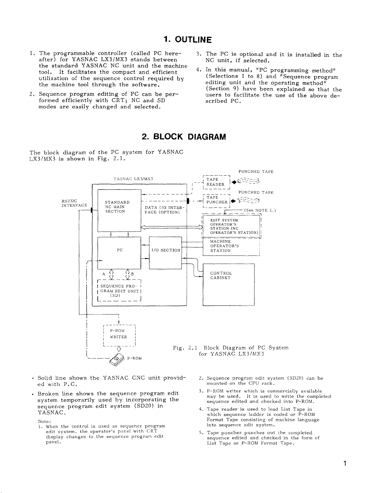
2. BLOCK
The block diagram of the PC system for YASNAC
LX31MX3 is shown in Fig. 2.1,
y~,s5.4cLx3/fJ~3
I ~-------- ---- ‘“~cHEcIT~pE
A
J t
r I —1 4
I l-l FH
I II II ~
1
Pc 1/(.)SECTION
3. The PC is optional and it is installed in the
NC unit, if selected.
4. In this manual,
(Selections 1 to 8) and “Sequence program
editing unit and the operating methodti
(Section 9) have been explained so that the
users to facilitate the use of the above described PC.
1!pc programming method”
DIAGRAM
.—— ———.
L ::------
I
EDITSYSTEM
I
OPERATOR’S
STATION(NC
2
OPERATOR’SSTATION)
——— ——-_ ___
MACHINE
OPER.ATOR’S
STATION
PUNCHED TAPE
I
I
I
I
A
9
~?.LY__3
ISEQUENCE PRO- i
1GRAy5~IT UNITI
L__––-– J
.
Solid line shows the YASNAC CNC unit provid- Z.
ed with P.C.
.
Broken line shows the sequence program edit
system temporarily used by incorporating the
sequence prog:ram edit system (SD20) in
YASNAC.
Note:
When the controlisused as sequence program
1.
editsystem, the operator’spanelwith CRT
displaychanges to the sequence program edit
panel.
J
CONTROL
CABINET
I
Sequence program editsystem (SD2(I)can be
mounted on the CPU rack.
P-ROM writerwhich is commerciallyavailable
3.
may be used.
sequence editedand checked intoP-ROM.
4,
Tape reader isused to loadListTape in
which sequence Iadderis coded or P-ROM
Format Tape consistingof machine language
intosequence editsystem.
Tape puncher punches out the completed
5.
sequence editedand checked in the form of
ListTape or P-ROM Format Tape.
Itis used to writethe completed
1
3.
SPECIFICATIONS
3.1 FUNDAMENTAL
(1)
Control method:
(2) Processing time:
Approx. 2.7 p see/step
High speed scanning time - 8 msec
.. .
Lou, speed scanning time – 8 msec K n (n is
determined by the capacity of the total
program. )
(3) Frogram memory capacity:
\lernory element:
Basic - 16K bytes
Optic,n -
16000 steps in basic instruction. )
(4) 1-ypes of instruction language:
~a~i~ instruction -
Ulacrc instruction –
32K bytes or 64K bytes
( b4K bytes corresponds to approximately
SPECIFICATIONS
Scanning method
EpROM (256 bits/one)
61 types
11 types
3.2 FROGRAM FUNCTIONS
( 1)
internal relay:
(? ) Register:
(3) Timer: 94 (5 types)
. 8 rnsec - 2.4 se,:, 20 ea.
.
53
msec – 12.75 see, 30 ea.
. 100 msec - 25.5 see, 30 ea.
.1
ssc – 255 sec , 10 ea.
n-in - 255
.1
(.4)
Sequencer parameter:
rein, 4 ea.
4000 points
500 (8 bits/one)
100
( 6) Pattern clear
( 7) Parity check
(8) Data conversion:
(~) Data search
Index data transfer
Message display
SUBP 009
SUBP 011
SUBP 014
SUBP 017
SUBp 0]8
SUBP 023 -Optional
function
lNPUT/ OUTPUT SPECI FICATIIONS
CPU built-in 1/0 boards (IC) boards)*
DC input:
Noncontact output: 64 points (Max. )
* CPU built-in 1/0 boards cannot be mounted to
A4X3.
(2) Optional standard 1/0 boards
DC input: 112 points
Noncontact output: 64 points
Reed relay output: 4 points
(3) CRT panel built-in !/0 boards (SP20 board)
DC input:
Non contact output:
m+1k$4
112 points (Max, )
64 points
32 points
Keep relay:
(5)
Keep memory:
(6)
MACRO INSTRUCTIONS
3.3
Following 11 types of macro instructions can be
used,
7200
900 (8 bits/memory)
lnstr~uctiorlword
( 1) l?ise signal detection:
(2) Fall signal detection:
(,3) Counter:
Fnnctions--Ring counter or
up–down counter.
Counting range--O - 9999
(4) Rotation
( 5) {;ode conversion
preset counter or
S’JBP 003
SUBP 004
EiLJBP 005
SUBP 006
SUBP 007
2
Note:
The detail of basic instructic~ns are given
i.
in the following table.
Type of Instruction
Relay instruction
1.
7
Register instruction
u,
Timer instruction ,
3,
4.
Control instruction
Tot
al
2.
Internal relays and registers are the same.
Addresses used as internal relays cannot ‘oe
used as internal relays.
2
Keep relays and keep memories are the same.
-,.
Addresses used as keep relays cannot be used
as ‘keep memories .
‘memories cannot “be used as keep relays.
Addresses used as keep
Instructions
I
t
!
I
~
lNO. of
13
37
2
9
~~
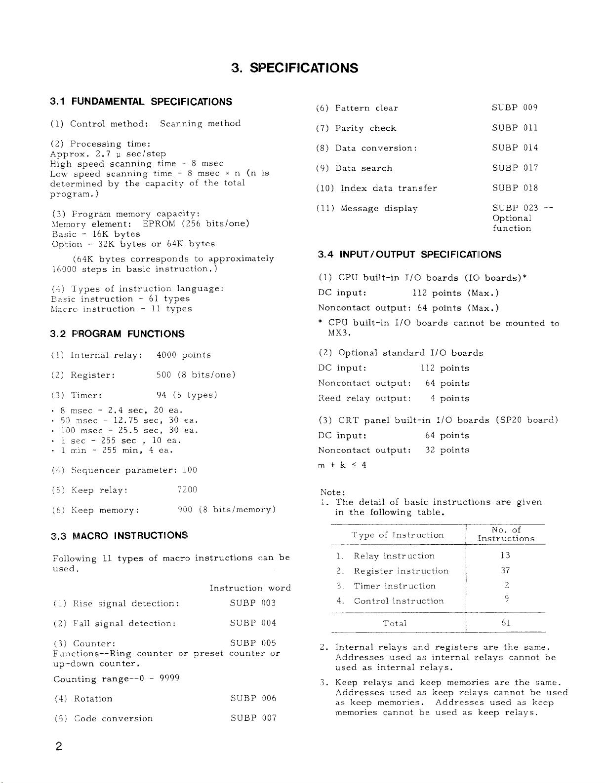
(4) 1/0 board location
3 1/0 boards are shown below.
YASNAC LX3/MX3
CPU Tu7LT-i
p%$~~.oUTP.T:40 Points
cN52
r“’
CN53 INPUT:
C?J54 INPUT:
CN55
‘1=
L___ -1
(THIS CAN NOT BE
!+OUNTEDON
INPUT:
_ INPUT:
—.
KSY SOASD CRT
[
Ua
8 Points
24 Points
40 Points
40 Points
.—
OUTPUT :
OUTPUT: 16 Points
CRT PANEL
“?+-E5Z!!!!
LINPUT. 48 Points Reed I-eI.Y outP.t)
I
1--1-
c~,l +l’’xc”-’o”~
.---._I ,
.—.
—1-
(5) Maximum number of 1/0 boards
. CPU built-in 1/0 boards ltiax. number 1
input:
output : 64 points (Max. ) *2
A
(FOR EXTENDED
INSTALLATION)
%
112 points (Max. )
~lNpUT16F’oints ;UTPUT:3, PoinLs
EXPANS1ON
EXTERNAL
110-BOASD -
CS12
CSICN CN3CN4CS5CN6
OUTPUT :
INPUT:
L
~OUTpUT: 40 F’oints
INPUT:
INPUT:
INPUT:
40 Points
40 Points
24 Points
8 Points
4 Points
8 Points
OUTPUT :
OUTPUT :
16 Points
8 Points
. External expansion 1/0 boards Max. number 4 *1
input:
output : 272 points
. CRT panel built-in 1/0 boards Max. number 1
input:
output : 32 points
* 1 When other I /O boards are additionaHy mounted J
the max.
boards becomes as follows:
CPU
built-in
1/() boards
CRT panel ~
built-in
1/0 boards [
Max. external
expansion
1/0 boards
*2 1/0 points of CPU built–in 1/0 boards are as
follows ;
1/0 20 boards (JANCD-1020-1) input:
1/0 20 boards (JANCD-1020-2) input:
1/0 20 boards (.TANCD-1020-3) input:
448 points
62 points
number of external expansion 1/0
without with
-u ‘
I without ~without
1
Max.4 ~
I
Max.: I Max.3 Max. 2
~without
..: .~
with ~ ,Uith
I
output : 48 points
output :
112 points
output : 64 points
with
48 points
88 points
48 points
3
4. PROCEDURES FOR SEQUENCE PROGRAM PREPARATION
‘Determine the specifications
of controlled operation.
Carry out assignment of
input/output signals be–
t~veen machine tool and
t
IMake se~uence ladder.
Perform coding by instruction language of PC.
1
PC.
I
Formulate the listtape by
the tape puncher.
‘--– ---4- -
I
——— ———
1
,
-._.
I
I
1
I
,
I
I
I
I
--J
—— —
Jt-l
Complete test operation for
the contents of RAM memary.
I
I
4’
Write the sequence program
through the connected
I
P–ROiM writer.
Complete final test run
+-l
I
through the contents of
1P-ROM.
1
Correct the se-
quence program.
>
,_J
t
——
I
II
Store the sequence program
of P-ROM format (klachine
language) in.RAivlmemory.
Perform editing of the se- I ‘
quence program while w,atch-
ing the display on the CRT \
(delete, input, change) .
a
a
A
I
L.
Note:
4
—
The sections surrounded byl _ _ _~require the “sequence program editing de~ricc (SD20) . “
— —.
I ——
(
,--------
End
——
Complete final correction of
the sequence ladder (1/0
list complete)
‘I
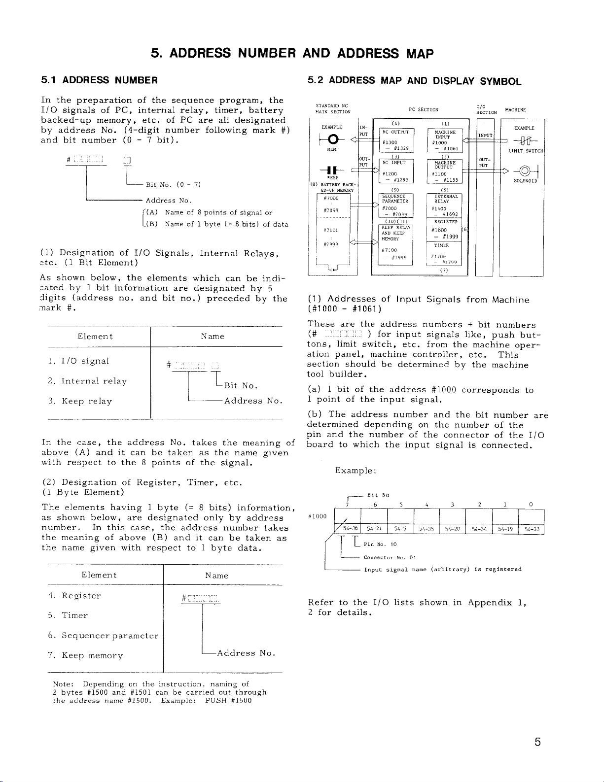
5. ADDRESS NUMBER
AND ADDRESS
MAP
5.1 ADDRESS NUMBER
In the preparation of the sequence program, the
1/0 signals of PC, internal relay, timer, battery
backed-up memory, etc.
by address No. (4-digit number following mark #)
and bit number (O – 7 bit) .
L-
of PC are all designated
BitNo. (O- 7)
~ Ad&.e~~ No,
(A) Name of 8 pointsofsignalor
?Jame of 1 byte (= 8 bits)of data
(B)
[
(1) Designation of 1/0 Signals, Internal Relays,
stc. (1 Bit Element)
As
shown below, the elements which can be indicated by 1 bit information are designated by 5
digits (address no.
.nark #.
.Element
1. 1/0 signal
2. Internal relay
3. Keep relay
In the case, the address No. takes the meaning of
above (A) and it can be taken as the name given
with respect to the 8 points of the signal.
(2) Designation of Register, Timer, etc.
(1 Byte Element)
The elements having 1 byte (= 8 bits) information,
as shown below, are designated only by address
number ,
the meaning of above (B) and it can be taken as
the name given with respect to 1 byte data.
In this case, the address number takes
Element
and bit no. ) preceded by the
Name
# :;.- ’.:.: :;
~lBit No.
1
Address No.
Name
5.2 ADDRESS MAP
STANDARD NC
MAIN SECTIO!4
FJAMPLE
Mm
1) BATTERYBACW
ED-UP MT.MORY
07000
#~~gq ~
II7101
~
~ #7Q99
(1) Addresses of Input Siqnals
(#1000 - #1061) -
These are the address numbers + bit numbers
(# ..::.::::;::
tons, limit switch, etc. from the machine operation panel, machine controller, etc.
section should be determined by the machine
tool builder.
(a) 1 bit of the address #1000 corresponds to
1 point of the input signal.
(b) The address number and the bit number are
determined depending on the number of the
pin and the number of the connector of the 1/0
board to which the input signal is connected.
//1000
/’l- T
( I L
k
11,.
OUT
II
)
Example :
,_ Bit No
;
/
/
54-21
54-36
pin N.. 10
ConnectorNo. 01
Input signalname (a~bitrary)is registered
6 5
AND DISPLAY SYMBOL
~
rom Machine
3
110
SECTION
NPU
lUTWT
2
t4.4CHINE
EX&+PLE
LIMIT SWITC)
1+
=’+
SOLENOID
F
I
This
1
PC SECTION
(4)
NCOKTPUT
Q1300
– 01329
c1
3
NC lNPCT
01200
- /11295
n
(9)
SEQUE!4CE
PARAMETER
//7000
- #7099
m ~’
(10)(11)
m3
for input signals like, push but-
56-5
(1)
MACHINE
lNPUT
#1000
- 81061
c1
m
khJ
(5)
lKTERNAJ.
RELAY
01400
4
54.35
54-20 54-34I54-19 5L-33
0
—
4. Register
5. Timer
#:::,:‘:”
I
I I
6. Sequencer parameter
7. Keep memory
Ifote: Depending on the instruction,naming of
2 bytes #1500 and #1501 can be carriedout through
the address
name #1500.
II
L
Address No.
I
Example: PUSH #1500
Refer to the 1/O lists shown in Appendix 1,
2 for details.
5
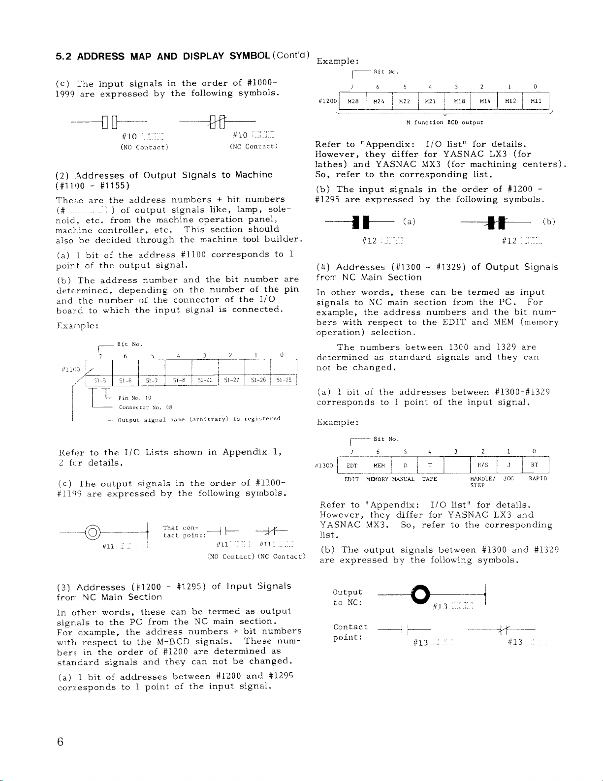
5.2 ADDRESS MAP AND DISPLAY SYMBOL ( Cent’d ) ~xampl~.
(c) The input signals in the order of #10001999 are expressed by the following symbols.
““””@+*l%I&la,
“--+ D-- JH7
#lo ‘ ‘::.:
(NO
Contact)
(~) ,4ddre~~es of output Signals to Machine
[#lloo - #1155)
These are the
(#. .
noid ,
machine controller, etc.
also be decided through the machine tool builder.
point of the output signal.
board to which the input signal is connected.
etc. from the machine operation panel,
(a) 1
bit of the address #1100 corresponds to 1
(b) “1’he address number and the bit number are
determined, depending on the number of the pin
and the number of the connector of the 1/0
Example :
address numbers + bit numbers
) of output signals iike, lamp, sole-
This section should
#lo ~ 1:::
Contact)
(NC
Refer to “Appendix:
Xowever, they differ for YASNAC LX3 (for
lathes) and YASNAC MX3 (for machining centers) .
So, refer to the corresponding list.
(b) The input signals in the orcler of #1200 -
#1295 are expressed by the following symbols.
---1 I ‘a’
(4) Addresses (//1300 - #1329) of Output Signals
from NC Main Section
In other words, these can be termed as input
signals to NC main section from the PC.
example ~
‘hers with respect to the EDIT and MEM (memory
operation) seleetion,
The numbers ‘oetween 1300 and 1329 are
determined as standard signals and they can
not be changed.
— Bit No.
———————--—-—
H function BCD output
1/0 list” for details.
–=#E--
the address numbers and the bit num–
(b)
For
l-----
Refer to the 1/0 Lists shown in Appendix 1,
2 for details.
(c) The output signals in the order of #1100 -
#11 cl’?are expressed by the following symbols.
-“”e-+
(3) Addresses (#1200 - #1295) of Input Signals
f~OIT NC Main Section
In c]ther words, these can be termed as output
signals to the PC from
For example,
with respect to the ,M-BCD signals.
bers in the order of #1200 are determined as
standard signals and they can not be changed.
(a) 1 bit of addresses between #1200 and ?/1295
corresponds to 1 point of the input signal.
Output signal name (azbitrary) is registered
%;:;:.:++-
/)11 ‘“-
the NC main sect:lon.
the address numbers + bit numbers
//11”..::.,
(NO Contact) (NC Contact)
-+”+
{}11. ....
These num-
(a) 1 bit of the addresses between #1300 -#1329
corresponds to 1 point of the input signal.
Exampie:
Bit So.
7 5
I
“’300El “m [ D I T
EDIT M1310RY MANL’AL TAPE
Refer to
However, they differ for YASNAC LX3 and
YASNAC MX3.
list,
(b) The output signals between #1300 and #1329
are expressed by the following symbols.
output
co
“.4ppendix: 1/0 list” for details.
SC:
54
I
So, refer to the corresponding
3
I
I-
H4NDLE/ JW RAPID
STEP
4
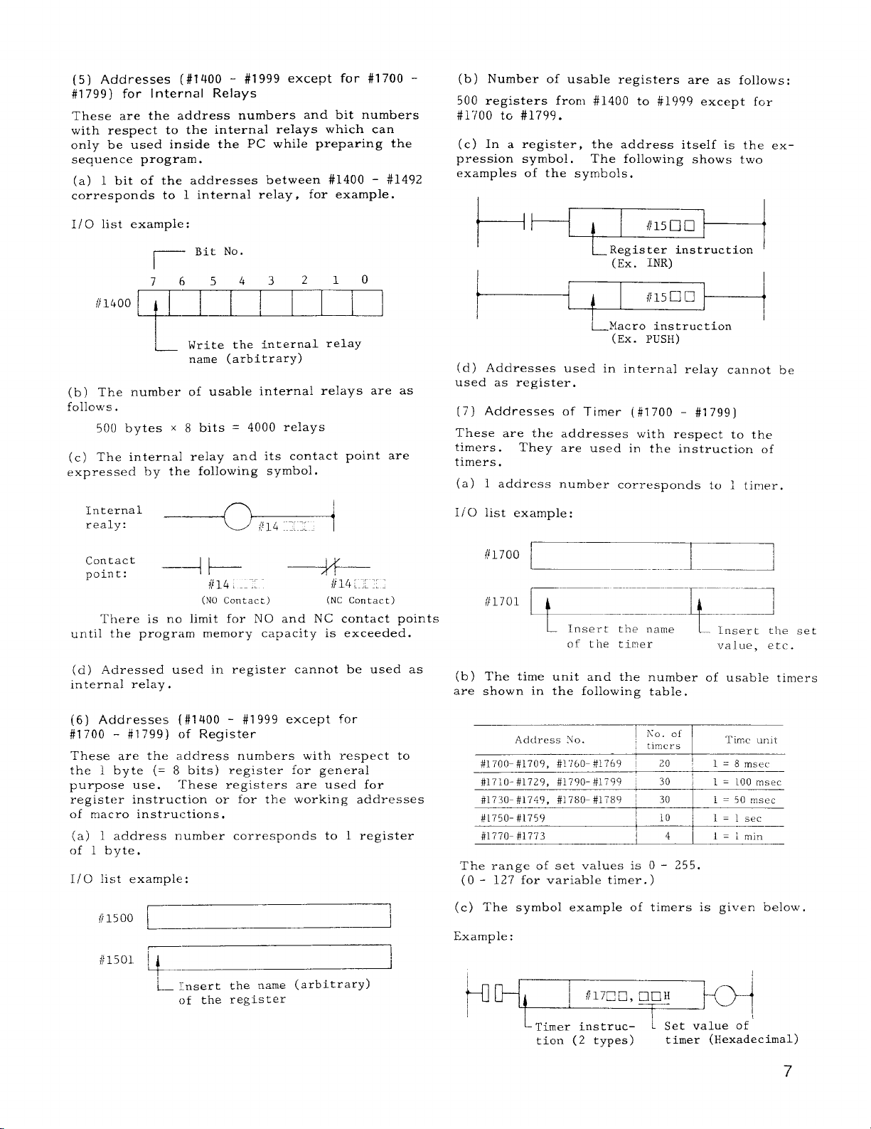
(5) Addresses (#1400 - #1999 except for #17’00 -
?/1799) for Internal Relays
These are the address numbers and bit numbers
with respect to the internal relays which can
only be used inside the PC while preparing the
sequence program.
(a) 1 bit of the addresses between #1400 - #1492
corresponds to 1 internal relay, for example.
(b) Number of usable registers are as follows:
500 registers from #1400 to #1999 except for
#1700 tG #1799.
(c) In a register,
pression symbol. The following shows two
examples of the symbols.
the address itself is the ex–
1/0 list example:
#15cla
4t
l-----+m-l
~Macro instruction ‘
“l’OO@iizz!?
name (arbitrary)
(b) The number of usable internal relays are as
follows .
500 bytes x
(c) The internal relay and its contact point are
expressed by the following symbol.
Internal
realy:
Contact
point:
There is no limit for NO and NC contact points
until the program memory capacity is exceeded.
8 bits = 4000 relays
—
–--1 t--
{114L..::-
(NO Contact)
.,.
{114.....
I
i
(d) Addresses used in internal relay cannot be
used as register.
[7) Addresses of Timer (#1700 - #1799]
These are the addresses with respect to the
timers.
timers.
(a)
1/0
They are used in the instruction of
1 address number corresponds to 1 timer.
list example:
#1701
Q-----–L---J
L ~nsert the name
of tile timer
(Ex. PUSH)
L Insert t!le set
value, etc.
Adressed used in register cannot be used as
(d)
internal relay.
(6) Addresses (#1400 - #1999 except for
#1700 - #1799) of Register
These are the address numbers with respect to
the 1 byte (= 8 bits) register for general
purpose use.
register instruction or for the working addresses
of macro instructions.
(a) 1 address number corresponds to 1 register
of 1 byte.
1/0 list example:
These registers
~ Insert the name (arbitrary)
of the register
are used for
The time unit and the number of usable timers
(b)
are
shown in the following table.
AclciressNo.
#1700-#1709,#1’160-#1769 : 20 ~
#1710-#1729,#1790-#179q
#1730-#1749,#1780-#1789 ~ 30
#1750-#1759
#1770-#1773
‘The range of set values is O - 255.
(O - 12’7 for variable timer. )
(c) The symbol example of timers is given below.
Example:
-’
! No, of
tmcrs
30 1 1 = LOO msec
! lo
I
Time unit
1 = 8 msec
1 = 50 mscc
l=lsec
l=lmin
LTimer in5truc- L Set value of
tion (2 types)
timer (Hexadecimal)
7
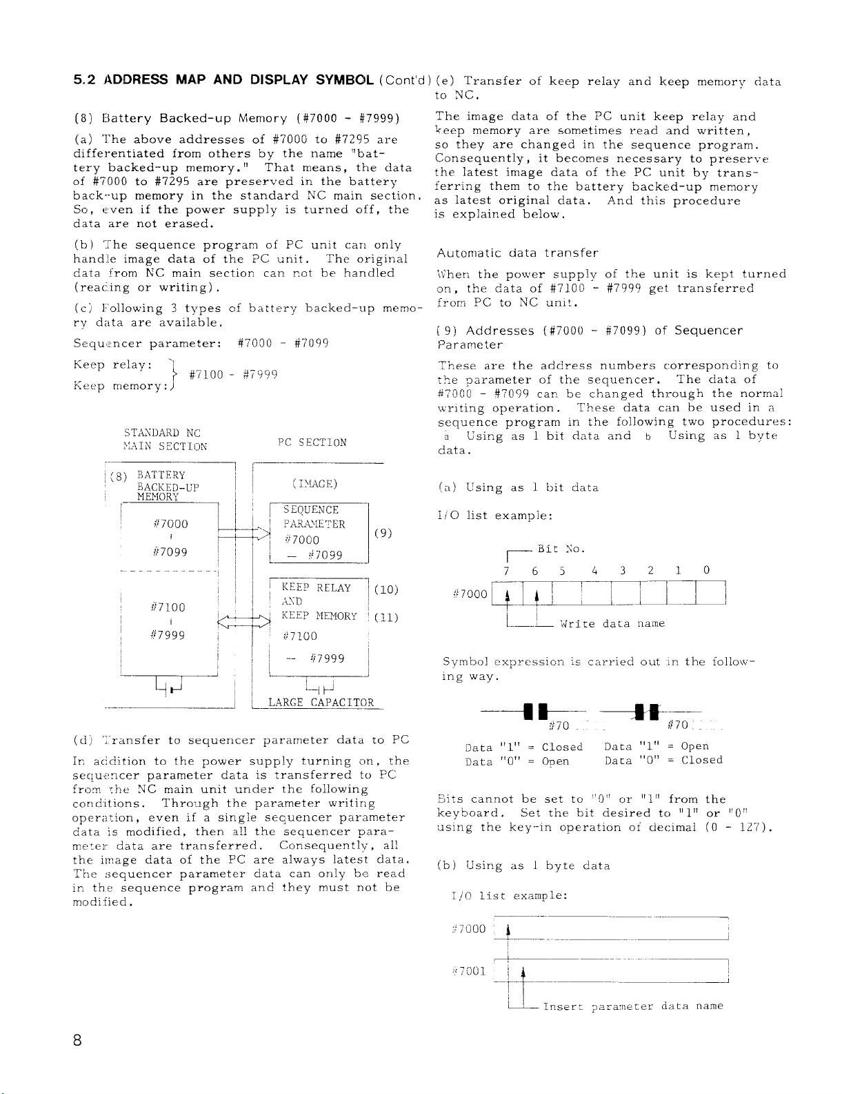
5.2 ADDRESS MAP AND DISPLAY SYMBOL (Cent’d ) (e) Transfer of keep relay and keep memory data
(8) 13attery Backed-up Memory [#7000 - #7999)
(a) The above addresses of #7000 to #7295 are
differentiated from others by the name “battery backed-up memory. ”
of #7000 to #7295 are preserved in the battery
back--up memory in the standard hTC main section,
So, even if the power supply is turned off, the
data are not erased.
That means, the data
(b) ‘The sequence program of PC unit can only
handle image data of the PC unit. The original
data from NC main section can rot be handled
(reac.ing or writing) .
(c) following 3 types of battery backed-up memo-
ry data are available ,
Sequlsncer parameter:
Keep relay:
Keep memory :
#7100 - #7999
}
STiLiI)ARDNC
}L\IX SECT IOX
~[8) BATTERY
BACKED–LT
MEMORY
I
7
#7000 -
~“—
#1’099
PC SECTION
(9)
-———
(10)
//7100
I
(17999
e
(
(11)
.—
to NC.
The image data of the PC unit keep relay and
Ikeep memory are sometimes read ,and written ,
so they are changed in the sequence program.
Consequently , it becomes necessary to preserve
the latest image data of the PC unit by transferring them to the battery backed-up memory
as latest original data.
is explained below.
Automatic data transfer
:Vher, the power
an, the data of #7100 - #7999 get transferred
from, PC to NTC ‘unit.
( 9) .Addresses (#7000 – #7099) of Sequencer
Parameter
These are the address numbers corresponding to
tb.e parameter of the sequencer.
li~t)(lo – #’7099 can be
supply of the unit is kept turned
\vrltingoperation .
And this procedure
The data of
changed through the normal
These data can be used in a
sequence program in the following two procedures:
2 Using as 1 bit data and ~
data.
(a) Using as 1 bit data
1/0 list exampie:
Bit No.
,l,ooofi-~ :413 i~’
i
L—–—
Write data name
Using as 1 byte
o
‘r
-—~ ~. LARGECAPACIWL
(d) ‘;’ransfer to sequencer parameter data to PC
In addition to the power supp]y turning on , the
sequencer parameter data is transferred to PC
from !he NC main unit under the following
conditions.
operation , even if a single sequencer parameter
data is modified,
meter data are transferred.
the image data of the PC are always latest data.
The sequencer parameter data can only be read
in the sequence program and they must not be
modified .
Through the parameter writing
then all the sequencer para–
Consequentl~; , all
Symbol expression is carried out [n the follow-
ing way.
Data “l” = Closed
Data “O” =
Sits cannot be set to “!3” or “l[! from the
keyboard. Set the bit desired to “ 1“ or “O”
using the key-in operation of decimal (O - 127) .
ODeI)
Data “l” = Open
I)ata “O” = Closed
(b) Using as 1 byte data
list example:
1,/0
,,
“7000
?7001
i
d.—... ...——..– —
-.
.+____ ___
II
~ Insert parameter data name
1
The symbol expression is the address number.
The example of using in timer is shown in the
following figure.
Example:
(a) 1 address number beyond #7100 corresponds
one keep memory of 1 byte (8 bits) .
1/0 list example:
to
~Variable timer
instruction
L Timer setting
by parameter
(10) Addresses (#7100 - #7999) of Keep Relay
These are the address numbers and bit numbers
of the keep relays used in the PC.
(a) 1 bit of #7100 - #7999 corresponds to 1 keep
relay.
1/0 list example:
Bit No.
r
76.54~2~ O
L Write the name of the keep relay
(b) The number of usable keep relays is as
follows.
900 bytes x 8 bits = 7200
(c) The keep relays and their contact points
are
expressed by the following symbols.
Contact
point
—--it ---- ~
#71 :::::.
(NO Contact)
//71::;[:
(NC Contact)
(11 ) Addresses [#7100 - #7999)
These are the addresses corresponding to the 1
byte memory which can be preserved even after
turning off the power supply.
formance is limited only to the preservation of
data, the keep memory can be used in the same
way as that of a register.
keep memory can also be used as an object of
register instruction or as supplementary data
of macro instruction.
preparing a sequence pr~gram for memory random
type ATC,
this keep meinory becomes necessary.
Especially, when
If the per-
Consequently, the
#7105 I
#7106
%
(b) The number of usable keep memory is as
follows :
900 memories from #7113(1to #7999
(c) The address number itself stands for the
.,
symbol
MOV:
of the keep memory.
t
Transfer the contents of register #1500
Write the name of the
keep memory
I
to keep memory #71 c;:.:
(12)
Writing Initial Values of
Keep Relays and
Keep Memories
When preparing a sequence program by using
the keep relays and keep memories, it becomes
necessary to set the initial values prior to
the execution.
(a) Set the system number switch of NC unit at
Ml!! and then turn on the power
(b) Depress the I DGNI function key.
Input /output signal ON /OFF state will be
displayed on the CRT screen.
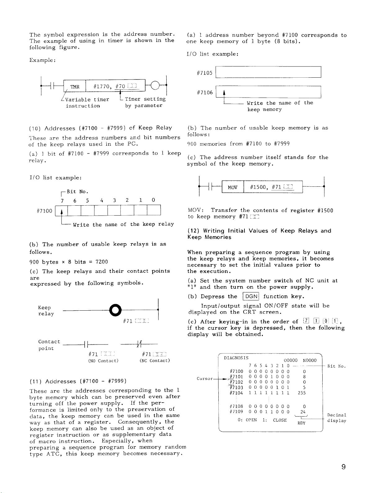
(c) After keving-in in the order of !fl ~ 10 ~r:
if the cursor- kc-y is depressed, then the following
display will be obtained.
DIAGNOSIS
76543210 —--—
I71OOOOOOOOOO o
O:
OPEN 1:
00001000
Cursor
-,y7101
#710200000000 o
‘77103 OOOOO1O1 5
#710411111111
I7108OOOOOOOO
#710900011000 24
00000 NOOOO
CLOSE
SIIFWIYo
8
255
o
~
RDY
Bit Ko.
Decimal
display
,
9
5.2 ADDRESS MAP AND DISPLAY SYMBOL ( Cent’d )
(d) Adjust addresses #7105 to #72$14 for initial
condition setting by depressing the cursor.
(e) ~f the \ INSRT1 (insert) key is depressed,
the cursor will move in the right hand direction,
and will move to the 7th bit position of the
address.
(f) Keep on pressing the cursor key until it
becomes adjusted to the position of the decimal
display.
(g) Key-in the desired ~ralues
tlng initialconditioriand then
key , The decimal display v-ill
the presently keyed in value .
—-——
(h) If the ~ lNSFiT ~k
ey is depressed, the cursor
will move to the left hand position #. Thereby,
the setting of one address number is conlpleted.
(i) lepeat steps (d) to (h) to write all the
desired initialvalues of the address numbers.
(j) +idjust the system number switch to “O.“
(0 - 255) for set-
depress the ~R–
get changed to
——
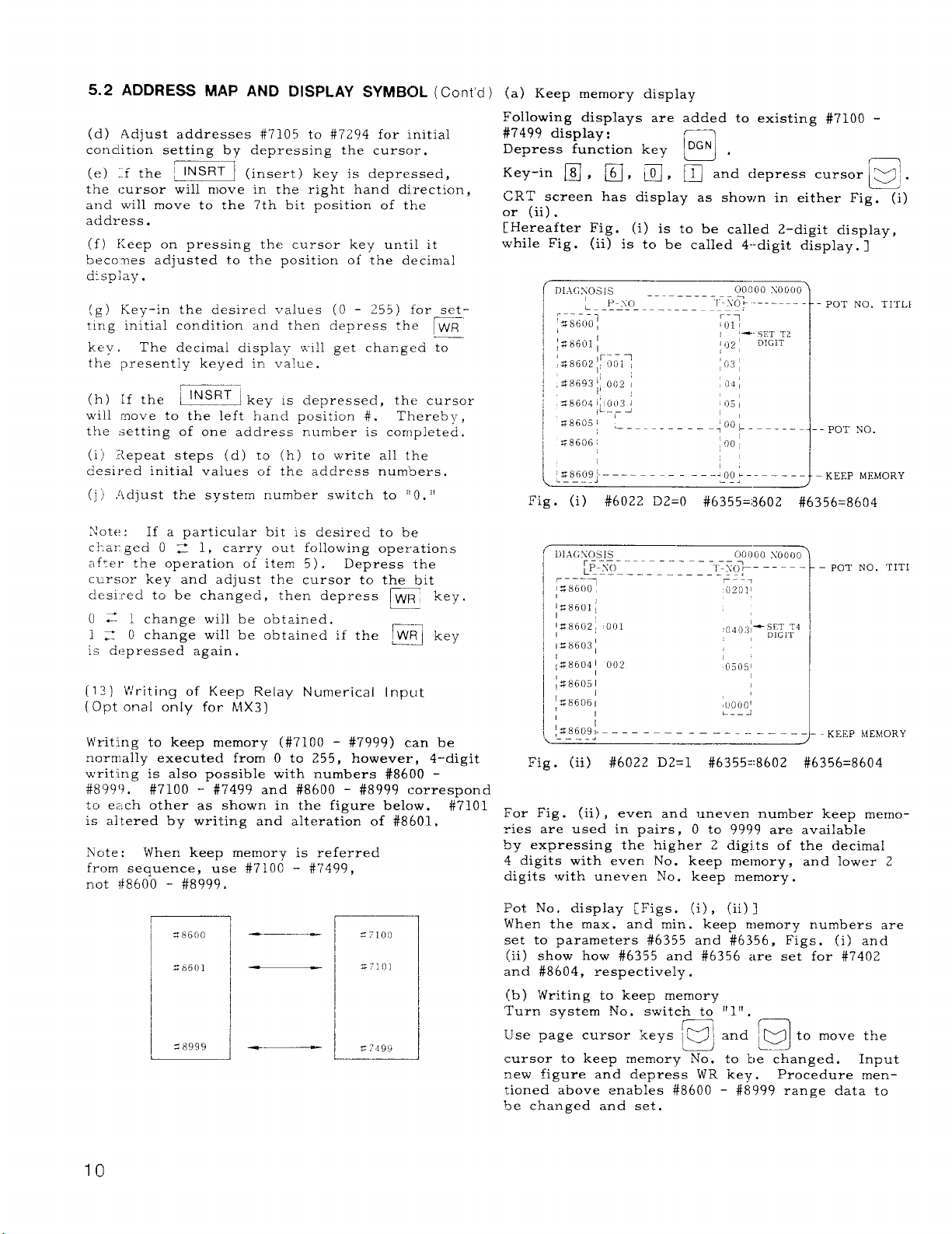
(a) Keep memory display
Following displays are added to existing #7100 #7499 dismlav:
Depress function key
Key-in ~ ,
,-
L
❑ , @ , ~ and clepress cursor ~ .
CRT screen has display as shown in either Fig
7
‘1!!! .
Wi)
or (ii),
[Hereafter Fig. (i) is to be called 2-digit display,
while Fig. (ii)is to be called 4--digitdisplay. ]
-POT NO. TITLE
-POT NO.
-KEEP MEMORY
. (i) #6022 D2=0 #6355=3602 #6356=8604
Note :
charged O z
If a particular bit is desired to be
1, carry out following operations
after the operation of item 5 ). Depress the
cursor key and adjust the cursor to the bit
desired to be changed, then depress
0=
change will be obtained.
1
i : 0 change will be obtained if the
~~ key.
~~ key
is depressed again.
(13) Vlt-iting of Keep Relay Numerical Input
(opt onal only for MX3)
Writing to
normally executecl from O to 255, however, 4–digit
writing is also possible with numbers #8600 -
#8999,
to each other as shown in the figure belc]w,
is altered by writing and alteration of #8601.
Note :
from sequence,
keep memory (#7100 - #7999) can be
#7100 - #7499 and #8600 - #8999 correspond
#7101
When keep memory is referred
use #7100 - #7499,
not j#860”0 – #8999,
~1
48600
=S601
=8999 1 +—
—4
— .—
l—
-– POT NO. TITI
~z86041 002
1$186051
;Z8606:
I
1
!28609!-––––––––– ___--. –— ___
(ii)
Fig.
For Fig. (ii) , even and uneven number keep memories are used in pairs , 0 to 9999 are available
by expressing the higher 2 digits of the decimal
4 digits with even No. keep memory, and lower 2
digits with uneven No. keep memory .
Pot No. display ~Figs. (i) , (ii) ]
When the max. and min.
set to parameters $6355 and #6356, Figs. (i) and
<ii) show how #6355 and #6356 are set for #7402
and #8604, respectively.
(b) Writing to keep memory
Turn system No. switch to “1“ .
Llse page cursor keys ‘~, and ~ ~ to move the
cursor to keep memory No. to be changed.
new figure and depress WR key.
tioned above enables #8600 - #8999 range data to
be changed znci set.
#6022 D2=1 #6355 =’8602 #6356=8604
Cljojl
,
,0000<
L-—J
– KEEP hiEh40RY
keep memory numbers are
7
L
Procedure men-
Input
10
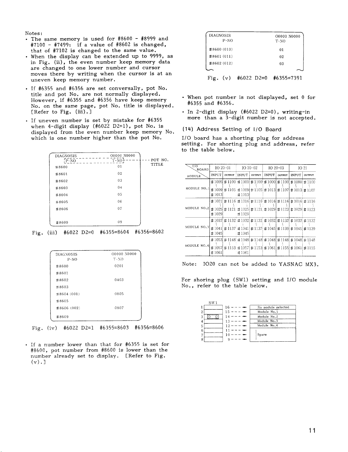
Notes:
.
The same memory is used for #8600 - #8999 and
#7100 - #7499:
that of #7102 is changed to the same value.
.
When the display can be extended up to 9999, as
in Fig. (ii), the even number keep memory data
are changed to one lower number and cursor
moves there by writing when the cursor is at an
uneven keep memory number.
.
If #6355 and #6356 are set conversally, pot No.
title and pot No. are not normally displayed.
However, if #6355 and #6356 have keep memory
No, on the same page, pot No. title is displayed.
[Refer to Fig. (iii). ]
.
If uneven num’ber is set by mistake for #6355
when 4–digit display (#6022 D2=1) , pot No. is
displayed from the even number keep memory No.
which is one number higher than the pot No.
%8600
#8601
#8602
#8603
#8604
K8605
#8606
if a value of #8602 is changed,
---POT NO.
01
TITLE
02
03
04
05
06
07
DIAGNOSIS
P-No
ti8600(010)
#8601(011)
#8602(012)
Fig. (v) #6022 D2=0 #6355=7391
. When pot number is not displayed, set O for
#6355 and #6356.
o In 2-digit display (#6022 D2=O) , writing-in
more than a 3–digit number is not accepted.
(14)
Address Setting of 1/0 Board
1/0 board has a shorting plug for address
setting.
to the table below,
For shorting plug and address, refer
~C1.,D~~O 20-01 IO20-02 I 1020-03
0“,,”, INPUT 0.,,.,
MODULE
‘~ODuLE‘0’1 #1009 $;105 ?$1009 $1105 ~#1013 #1107 @lh13~# 1107
INPUT
lpo5# 1,100$1000# 1,100!$1000# 1)00#looo~Flloo
#
#lo13
‘1’”1 ~ ‘
$10131
00000NOOOO
T-NO
01
02
03
1()q
INPUT OUTPUT INPuT OUTPUT
,,
#1021$1116$10161~1116’#1016#1116+lld#ll16
‘iODuLE‘0.2#loJ5Al $Iokl;l tiloJ9#ll;3wo&l;3
#8609
Fig. (iii) #6022 D2=0 #6355=8604 #6356=8602
DI.AGXOSIS
P-NO
#8600
09
00000Xoooo
T-XO
0201
#8601
#8602
0403
?$8603
$8604[001)
0s05
$18605
#8606(002)
0807
88609
Fig. (iv) #6022 D2=1 #6355=8603 #6356=8606
.
If a number lower than that for #6355 is set for
#8600, pot num]ber from #8600 is lower than the
number already set to display.
(v). ]
[Refer to Fig.
XI -
#1037$1132$1032fi1132’a1032#1132#l~3m
# 1053~1148’$1048
$ 1;48!$1048
# 11481# 1~8~$1:148
“ODuLE‘0”4 # 1057+A53 $l@57$1153~#1061#1155#106i~#l155
# 1061
Note: 1020 can not be added to YASNAC MX3.
For shoring plug (SW1) setting and 1/0 module
No. . refer to the table below.
SM’1
1
2
3 a
4
5
6
7
8
16 ----
~j-––-
~4– –-_
13––– 12––– ll––– -
4
lo–––-
~–––_
41061
NO moduleselected
ModuleNo.1
I ispare I
11
5.2 ADDRESS MAP AND DISPLAY SYMBOL (Confd )
CRT Panel Built-in 1/0 Board
‘\.,
\t
Input
Area
No. i
SP 20-02
Input
r
output
\ 1-1 !*1I3O)-Z1OO7‘$lloo-#llo3
For shorting plug (SW2) setting and I/o area No.
refer to the table below.
16––
~j––
l!––
13––
~2––
~1––
lo––
9––
?:.,%,,.No, selected
.AreaNo.1-I
AreaNo.1-2 I
m
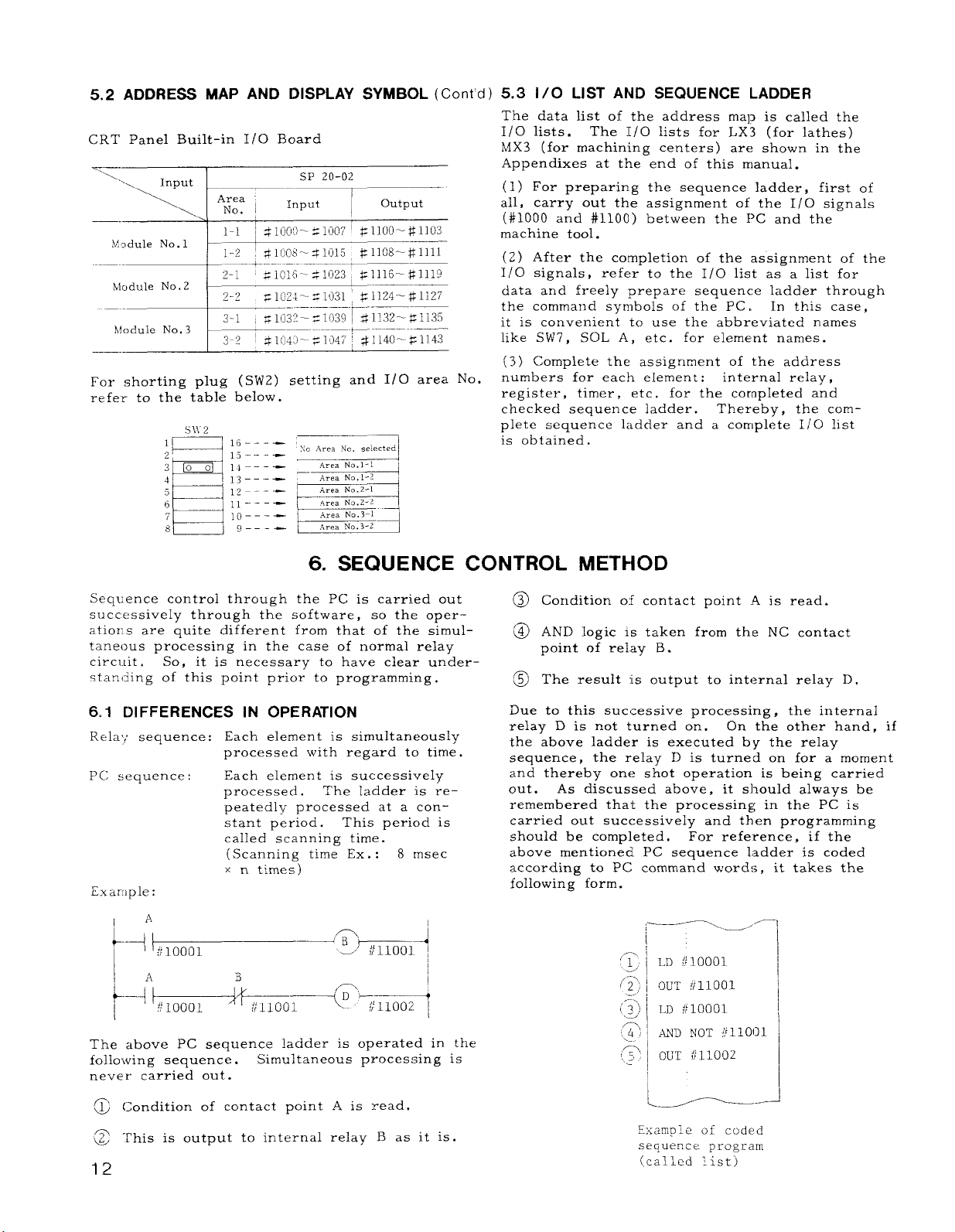
5.3 I/0 LIST AND SEQUENCE LADDER
The data listof the address map is called the
1/0 lists. The [/0 lists for LX3 (for lathes)
MX3 (for machining centers) are shown in the
Appendixes at the end of this manual.
(1) For preparing the sequence ladder, first of
all, carry out the assignment of the 1/0 signals
(#~000 and #1100)
machine tool.
(2) After the completion of the assignment of the
1/0 signals, refer to the 1/0 list as a list for
data and freely :prepare sequence ladder through
the command symbols of the PC, In this case,
it is convenient to use the abbreviated names
like SW7, SOL A, etc. for element names.
(3) Complete the assignment of the address
numbers for each element: internal relay,
register, timer, etc.
checked sequence ladder. Thereby, the com-
plete sequence ladder and a complete 1/0 list
is obtained.
between the PC and the
for the completed and
6. SEQUENCE CONTROL METHOD
Sequence control through the PC is carried out
successively through the software, so the operations are quite different from that of the simultaneous processing in the case of normal relay
circluit. So, it is necessary to have clear understanciing of this point prior to programming .
6.1
DIFFERENCES IN OPERATION
Relay
sequence:
PC Sequence:
Example:
1A
~.-+
;/10001
‘
1A
**fi?z-lToo2. ~
~-–~
I
Each element is simultaneously
processed with regard to time.
Each element is successively
processed.
The ladder is repeatedly processed at a constant period.
This period is
called scanning time.
(Scanning time Ex .: 8 msec
x n times)
I
—’P
J #llool ,
B
+
I
@ Condition of contact point .A is read.
@ AND logic is taken from the NC contact
point of relay B.
@ The result ‘1s output to internal relay D.
Due to this successive processing , the internal
relay D is not turned on. On the other hand, if
the above ladder is executed b y the relay
sequence,
and thereby one shot operation is being carried
out.
remembered that the processing in the PC is
carried out successively and then programming
should be completed.
above mentioned
according to PC
following form.
the relay D is turned on for a moment
As discussed above, it should always be
For reference, if the
PC sequence ladder is coded
command u’ords, it takes the
i~.~’-–
I
/-\
LD ;I1OOO1
1
I
-.
The above PC sequence ladder is operated in
following sequence.
never carried out.
@ (~ondition of contact point A is :read.
This is output to internal relay B as it is.
z
Simultaneous processing
12
the
is
~
Example of coded
sequence program
{called list)
—
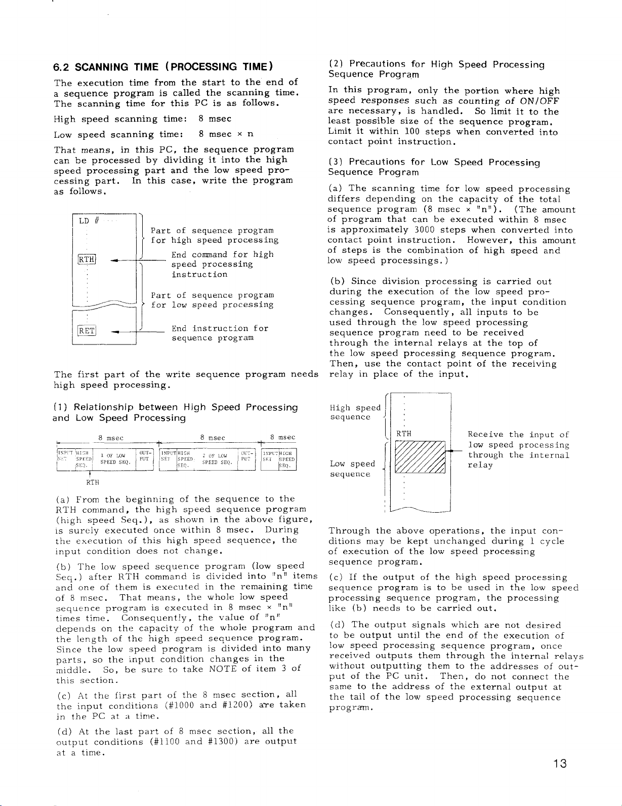
6.2 SCANNING TIME ( PROCESSING TIME)
The execution time from the start to the end of
a sequence program is called the scanning time.
The scanning time for this PC is as foHows.
High speed scanning time:
Low speed scanning time:
That means, in this PC, the sequence program
can be processed by dividing it into the high
speed processing part and the low speed pro-
cessing part.
as follows.
I LD {i
m —-
In this case, write the program
Part of sequence program
~ forhigh speed processing
I
J
8 msec
8 msec x n
End command for high
speed processing
instruction
tr
L’
-I I
_~ Part of sequence program
for low speed processing
End instruction for
P –+- ‘equence program
The first part of the write sequence program
high speed processing.
needs
(2) Precautions for High Speed Processing
Sequence Program
In this program, only the portion where high
speed responses such as counting of ON/OFF
are necessary, is handled.
least possible size of the sequence program,
Limit it within 100 steps when converted into
contact point instruction.
(3) Precautions
Sequence Program
(a) The scanning time for low speed processing
differs depending on the capacity of the total
sequence program (8 msec x ‘Jntl).
of program that can be executed within 8 msec
is approximately 3000 steps when converted into
contact point instruction. However, this amount
of steps is the combination of high speed and
low speed processing.)
Since division processing is carried out
(b)
during the execution of the low speed processing sequence program, the input condition
changes.
used through the low speed processing
sequence program need to be received
through the internal relays at the top of
the low speed processing sequence program.
Then, use the contact point of the receiving
relay in place of the input.
for Low Speed Processing
Consequently, all inputs to be
So limit it to the
(The amount
(1) Relationship between High Speed Processing
and Low Speed Processing
—–- ––—
(a) From the beginning of the sequence to the
RTH command,
(high speed Seq.), as shown in the above figure,
is sureiy executed once with.in 8 msec.
the execution of this high speed sequence, the
input condition does not change.
(b) The low speed sequence program (low speed
Secl.) after RTH command is divided into “n” items
and one of them is executed in the remaining time
of 8 msec.
sequence program is executed in 8 msec x “n”
times time.
depends on the capacity of the whole program and
the length of the high speed sequence program.
Since the low speed program is divided into many
parts, so the input condition changes in the
middle.
this :section.
(c) lit the first part of the 8 msec section, all
the input conditions (#1000 and #lZOO) are taken
in the PC at a time,
(d) At the last part of 8 msec section, allthe
output conditions (#1100 and #1300) are output
at a time.
8 msec
RTH
the high speed sequence program
That means, the whole low speed
Consequently, the value of “n”
So, be sure to take PJOTE of item 3 of
8 msec
~8 msec
During
tIigh speed~ :
sequence
RTH
I
‘
\
LOW speed
sequence
Through the above operations, the input con–
ditions may be kept unchanged during 1 cycle
of execution of the low speed processing
sequence program.
(c) If the output of the high speed processing
sequence program is to be used in the low speed
processing sequence program, the processing
like (b) needs to be carried out.
(d) The output signals which are not desired
to be output until the end of the execution of
low speed processing sequence program, once
received outputs them through the internal relays
without outputting them to the addresses of out–
put of the PC unit.
same to the address of the external output at
the tailof the low speed processing sequence
program.
~
Receive the input of
low speed processing
through the internal
relay
Then, do not connect the
13
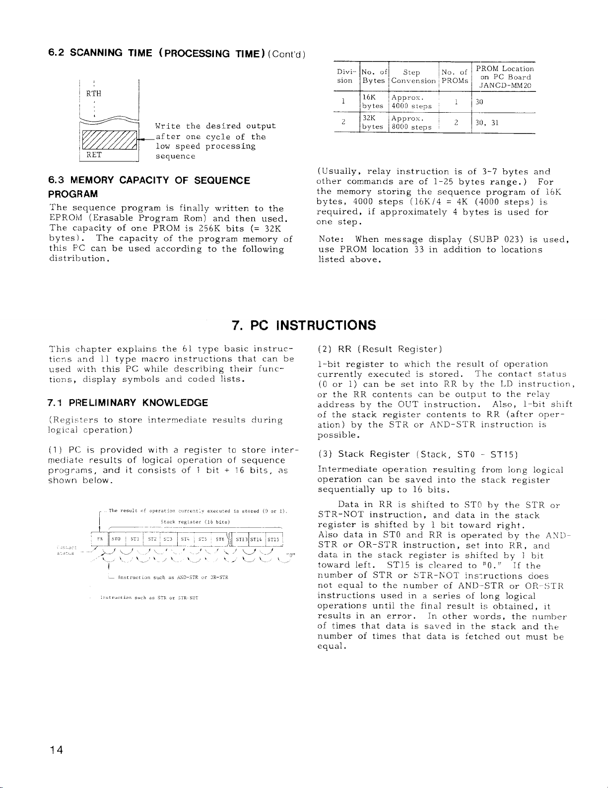
6.2 SCANNING TIME ( PROCESSING
TIME)
(Cent’d)
I’Jo.
Division Bytes ~Convension ~PROMs
~fl step
I
iNO, of
PROM Location
on PC Board
.JANCD-MM20
Write the
after one
low speed
desired output
cycle of the
processing
sequence
6.3 MIEMORY CAPACITY OF SEQUENCE
PROGRAM
The sequence program is finally written to the
EPROM (Erasable Program Rem) and then used.
The capacity of one PROM is 256K bits (= 32K
bytes ) .
The capacity of the program memory of
this PC can be used according to the following
distribution.
7. PC INSTRUCTIONS
This chapter eXpklnS the 61 type basic instructions and 11 type macro instructions that can be
used with this PC while describing their functions, display symbols and coded lists.
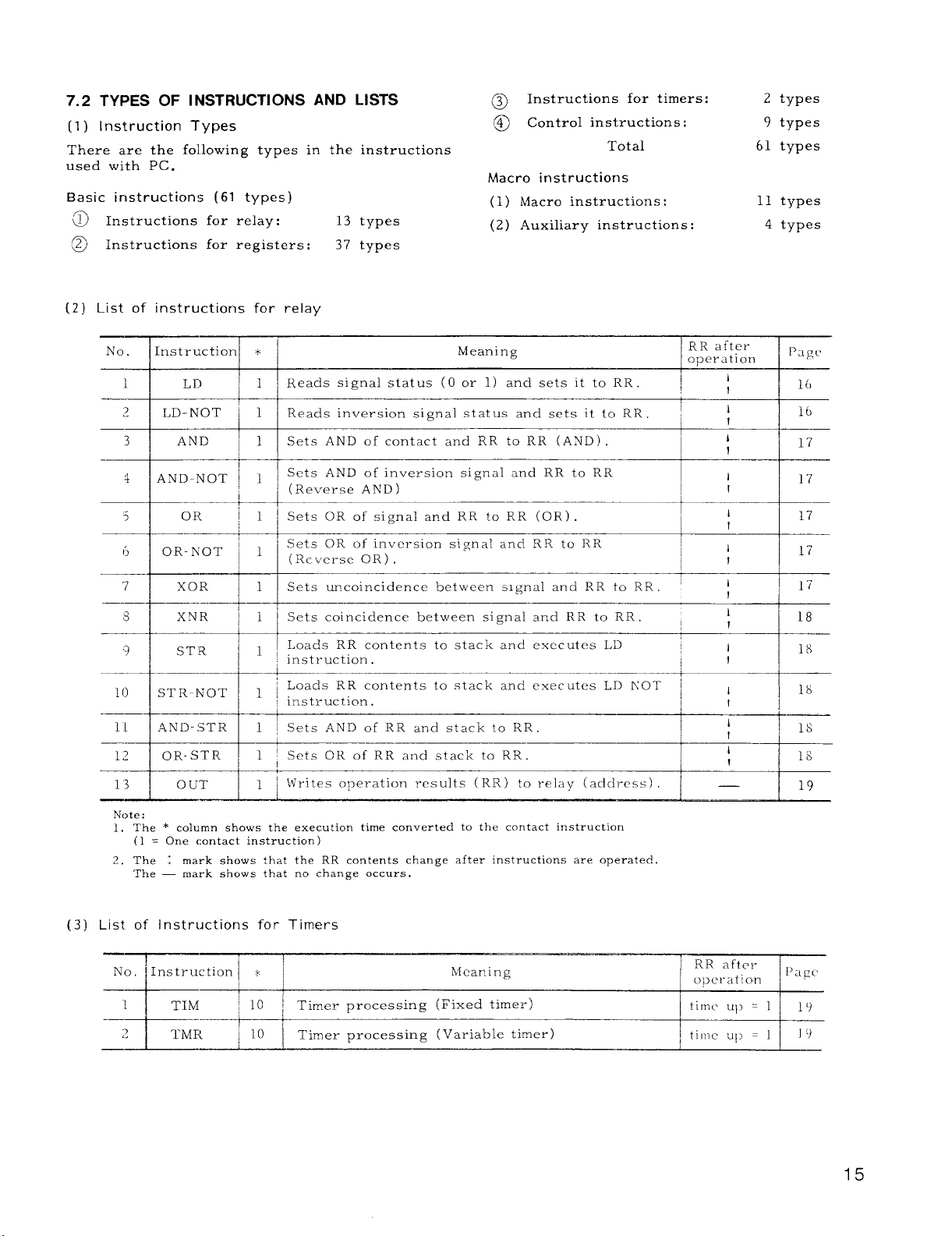
7.1 PRE LIMI NARY KNOWLEDGE
(Registers to store intermediate resuits during
logical cperation)
(1 ) PC is providecl with a register to store inter
mediate results of logical operation of sequence
programs,
shown below.
and it consists of 1 bit + 16 bits, as
(Usually, relay instruction is of 3-7 bytes and
other commands are of 1-25 bytes range. ) For
the memory storing the sequence program
bytes, 4000 steps (16 K/4 = 4K (4000 steps) is
required, if approximately 4
bytes is used for
of 16K
one step .
Flote:
When message display (SUBP 023) is used,
use ~ROM location 33 in addition to locations
listed above.
(2) RR (Result Flegister)
l-bit register to which the result of operation
currently executeci is stored.
(O or 1) can be set into RR by the LD instruction,
or the RR contents can be OUtp Ut to the relay
address by the C}LTT instruction.
of the stat’k register contents to RR (after oper–
ation) ‘by the STi?.or .4ND– STR instruction is
possible.
(3) Stack Register (Stack, STO - ST15)
Intermediate operation resulting from long logical
operation can be saved into the stack register
sequentially up to 16 bits.
Data in RR is shifted to STCI by the STR or
ST R-NOT instruction, and data in the stack
register is shifted by 1 bit toward right.
Also data in STO and RR is operated by the As 11STR or OR– STR instruction , set into RR , and
data in the stack register is shifted by 1 bit
toward left.
STI.5 is cleared to “O.“ If the
number of STR or ST R–h”OT instructions cioes
not equal to the number of AN D-STR or OP.–STR
instructions used in a series of long logical
operations until the final result
results in an error. In other words, the number
of times that data is saved in the stack and the
number of times that data is fetched out must be
equal.
The contact status
Also ,
is obtained , It
l-bit shift
14
7.2 TYPES OF INSTRUCTIONS AND LISTS
(1)
Instruction Types
There are the following types in the instructions
used with PC.
Basic instructions (61 types)
Instructions for relay:
a)
Instructions for registers: 37 types
a
(2)
List of instructions for relay
13 types
@
Instructions for timers:
Q
Control instructions:
Total
Macro instructions
( 1) Macro instructions:
(2) Auxiliary instructions:
2 types
9 types
61 types
11 types
4 types
No. Instruction * Meaning
L
~
3 AND 1 Sets AND of contact and RR to RR
3=
4 AND-NOT ~ 1
5 OR ~ 1 ~ Sets OR of signal and RR to RR (OR) .
6 OR-NOT
‘7 XOR
g’
8 XNR ~ 1 Sets coincidence between signal and RR to RR
9
F
10 ST R-NOT
11 AN D-STR
12
13 0 LiT
—
~z- ~ + -
Note:
1. The * column shows the executiontimeconvertedto the contactinstruction
(1 = One contactinstruction)
2. The ; mark shows that the RR contentschange afterinstructionsare operated.
The — mark shows that no change occurs.
LD
LD-NOT 1
ST-R 11,
OR-STR
11 Reads signal status (O or 1) and sets it to RR.
Reads inversion signal status and sets itto RR ~
Sets AND of inversion signal and RR to RR
I (Reverse AND)
‘ Sets OR of inversion signal and RR to RR
(Reverse OR)
1
Sets uncoincidence between signal and RR to RR
Loads RR contents to stack and executes LD
; instruction.
: Loads RR contents to stack and executes L12 NOT i
1 ~ instruction
1 ~ Sets AND of RR and stack to RR.
1 ~ Sets OR of RR and stack to RR.
1 \Urite~Omeration results (RR) to relay (address)
11
—
—.
11
—~
(AND) .
—~ ‘
-4 i
RR after
operation
I
I
I
!
i
I
I
1
I
I
!
I
I
i
I
I
!
Page
16
16
17
18
18
18
—
18
18
19
List of instructions for Timers
(3)
I 10 I Timer processing (Variable timer)
k[eaning
~ Timer processing (Fixed timer) time ul> = 1
—
RR after
Opel-ation
~ time u[) = 1
~~:,gc
1()
]c)
7.2 TYPES OF INSTRUCTIONS AND LISTS (Cent’d )
(4] List of instructions for Registers
[
IN R
1
2 DCR !3~ Adds - 1 to register contents.
3 CLR
-+’
-7
---+ i
‘+
—
=:;
-:+
——~——
4
ClvlR 3
;I ADI ~
6
7
8
9
10
11 \
12
13
14
15 ADD
16 SUB
17
19
20
SBI
AN- I
0J31
—~—,–
XRI
DEC 3! Coincidence of register contents and numeric. ]
CO I ~ 4 i Coincidence of register contents and numeric.
CMP :3’ Comparison of register contents and numeric .
CPI ~
MVI
ANR.
ORR
XRR
CPR 5
‘-i~ ‘ ~S.. he ,S. in R!+
–+—~——
I
22
-fi~?; ~
24
-1
25 i
MOV
—y
DIN
ADG
‘
3 ~ Adds + 1 to register contents.
z~
3 ! Addition of register contents and numeric.
3 I Subtraction of
3 AND
3 ~ OR of register contents and numeric.
3 ~ xOR of register
4 \ Comparison of register contents and numeric.
i3~
~ 4 ~in R2,
i 4 ~~.R2.
*“
-1
~1~
I
!Ji
4 ~
4
~“
~
Clears the register contents .
~ Inverts the register contents .
register contents and numeric
of register contents and numeric.
contents and numeric
Load numeric to a register.
Adds registers Ill and R2 and stores the result ,
Subtracts RI from R2 and stores the result
Takes
In R2.
Takes OR of RI and R2 and stores the result
in R2.
Takes XOR of RI and R2 and stores the result
in R2.
Checks the result o.fcom arisen Of RI with Rz, I
~
and stores the result in . 2.
Checks coincidence bet~veen RI and R2, and
Transfers R1 contents to R2.
Transfers AiND of RI contents and numeric to
R2.
;
Data extraction
Double Iengih addition
AND-(>f R1 and R2 and stores the result
. .
-~
+: ~;
,
-T
–- I 20
!
I
~ ‘-
I
—-
I
-- I
“’x
,*
f
i;
I
I
I
1
—-
—-
—-
4
$
--
I*
f
-
1 1 23
I
“~~+
\
—-
—.
!-+
14!
i
i
4
z
-y
I
I 21
21
1-
I 21
I 22
22
22
22
22
22
i 74
1-
—
16
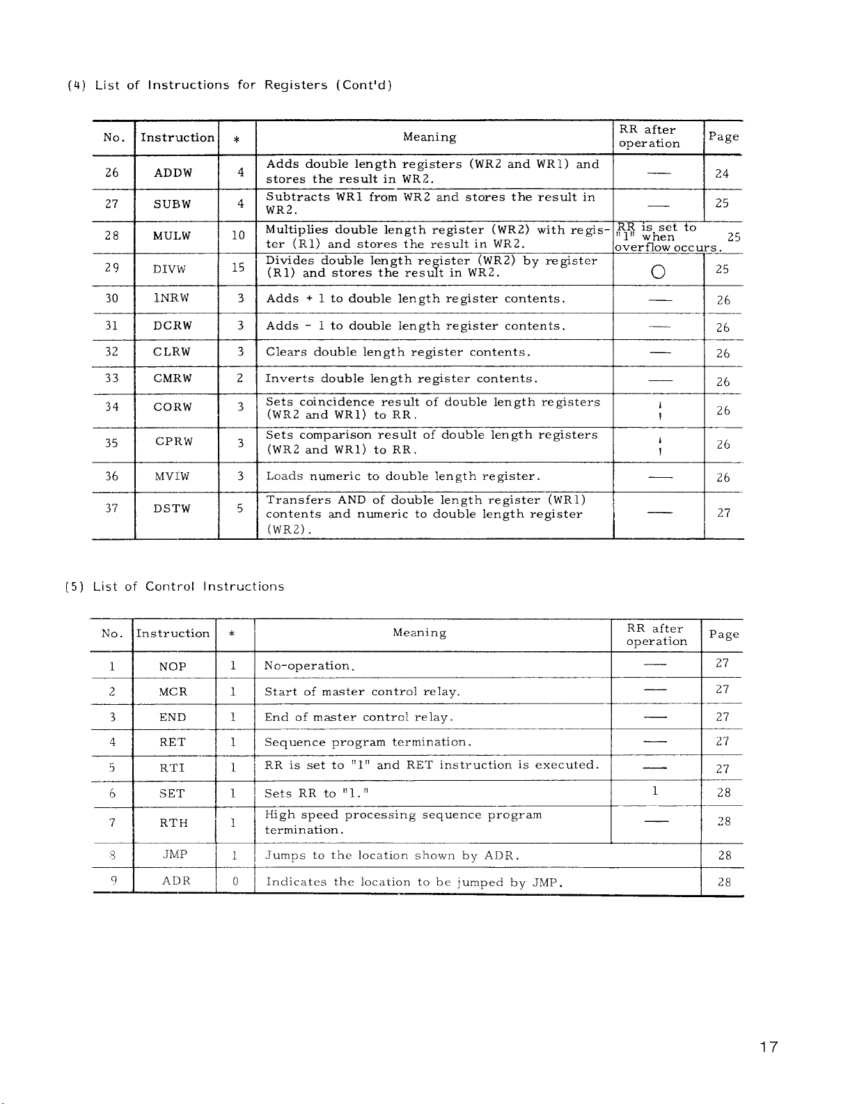
List of Instructions for Registers (Cent’d)
No. [nstructiol
26 ADDW
27
28
29 15
30
32 CLRW 3 Clears double length register contents.
33
——
34
35
36
37 5
SUBW
MUI.W
DIVW
lNR.W
DCRW
CMRW 2 Inverts double length register contents.
CORW
CPRW
MVI:W
——
DSTW
*
Adds double length registers (WR2 and WR1) and
4
Subtracts WR1 from WR2 and stores the result in
4
:::’heres”’tin’~l+
Multiplies double length register ( wR2) with re gis–
10
ter (Rl) and stores the result in WR2.
Divide
s double length register (WR2)
(Rl) and stores th= restit in WR2.
3 Adds + 1 to double length register contents.
3 Adds - 1 to double length register contents.
coincidence result of double length registers
Sets
3
(WR2 and WR1) to RR.
Sets comparison result of double length registers
3
(WR2 and WR1) to RR.
Loads numeric to double length register.
3
Transfers AND of double length register (WR1)
contents and numeric to double length register
(WR2) .
Meaning
by register
RR after
operation
RR is set to
,1Ill when
overflow (-
------
o
l—
l–
l–
l—
1
I
l—
I
i
I
C)ccl
Page
s.
25
26
26
26
26
26
26
26
27
25
(5)
List of Control Instructions
No. nstruction
——
——
NOP
MCR
END
RET
RTI
SET
RTH
JIUIP
ADR
1
—.
2 Start of master control relay.
*
1
.
No-operation.
1
1 End of master contrcl relay. 27
Sequence program termination.
1
RR is set to “1” and RET instruction is executed.
1
1
RR to “l. “
Sets
High speed processing sequence program
termination.
Jumps to the location shown by ADR.
Indicates the location to be jumped by JMP.
Meaning
++
RR after
o~eration
l–
l–
I
Page
I 27
I 27
27
_
27
r
I 28
28
17
7.2 TYPES OF INSTRUCTIONS AND LISTS (Cent’d )
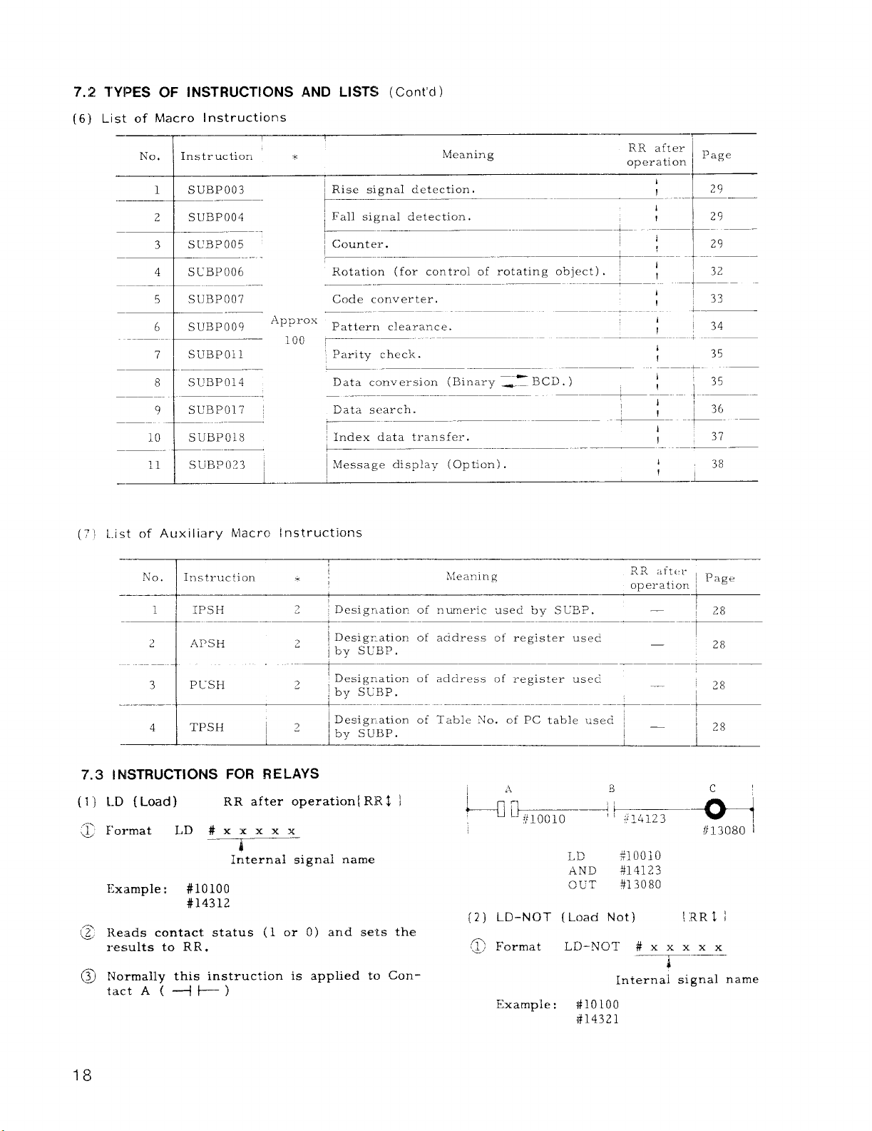
(6) List of Macro Instructions
No.
Instruction
1 SUBPO03
2 SUBPO04
SUBPO05
3
SUBPO06
4
5
SUBPO07
5[jBpoo9
6
SIJBPO1l
7
8
S(!BP017 !
9
10
SUBP018
SUBP023 I
——.
.
.Appl-ox
*
--—–—
100
—— ——
I
~—
IMessage display (Option).
(7) List of Auxiliary Macro Instructions
Meaning
Rise signal detection.
Fall signal detection.
.—.-.—-t.
Counter.
Rotation (for control of rotating object).
Code converter.
.-
——- ——
Pattern clearance.
Parity check.
Data conversion (Binary _- 13CD. )
——–—— -—
Data search.
-. –—
Index data transfer.
RR after
operation
I
I
1
~
I
1
I
I
1
I
I
1
I
J
I
I
I
I
I
!
Page
29
29
29
32
33
34
35
35
36
37
38
—
NO.
Instruction =
I
Denigration of numeric used by SUBP,
Desigr. ation of address cf re@ster used
by
SUBP.
Designation of adciress of register used
by SLBP.
Denigration of Table No. of PC table used ~
by SUBP.
7.3 1NSTRUCTIONS FOR RELAYS
(1) 1.D (Load) RR after operation{ RR $ ]
‘-’ Format~ LD#xx xxx
Example:
~ Reads contact status ( 1 or O) and sets the
results to RR.
@ Normally
tact A (
————
4
Internal signal name
#loloo
#14312
this
instruction is applied to Con-
++)
[2) LD-NOT [Load Not)
m Format
‘w,’
Example:
LD-No’I # x x x x x
Internal signal name
j#~oloo
{#14321
!—128
—.—
i 28
I
28
—
~ 28
!:RRtl
d
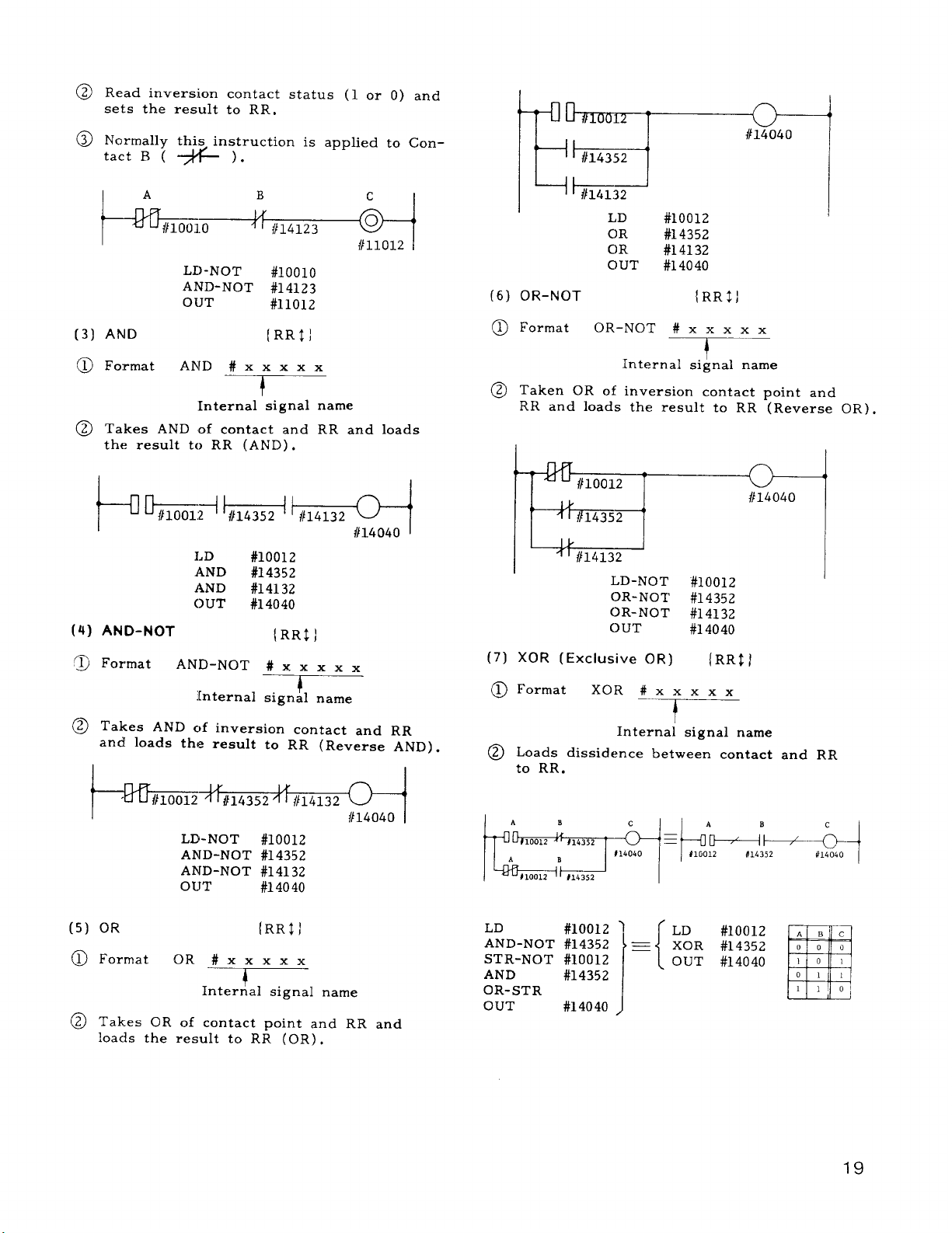
Read inversion contact status (1 or O) and
sets the result to RR.
Normally this instruction is applied to Contact B ( -~~~ ).
#14040
#14352
I
LD-NOT
AND-NOT #14123
OUT
Format
Takes AND of contact and RR and loads
the result to RR (AND).
1+
I
(4)
AND-NOT
Format
Takes AND of inversion contact and RR
and loads the result to RR (Reverse AND) .
AND#xx xxx
Internal signal name
kid w hi+---l
LD
AND
AND
OUT
AND-NOT
Internal
#loolo
#llo12
I
#loo12
#14352
#14132
#14040
!
signal name
//11012 I
{/14040 I
E“’oo”04
I
(6)
OR-NOT
@ Format
@ Taken OR of inversion contact point and
RR and loads the result to RR (Reverse OR) .
- #loo12
#)
(7)
XOR (Exclusive OR)
Format
Loads dissidence between contact and RR
to RR.
#14132
LD
OR
OR
OUT
OR-NOT #xx xxx
Internal signal name
1}
41
#14352
1}
-f
1#14132
XOR#xx xxx
4I
1
LD-NOT #10012
OR-NOT #14352
OR-NOT #14132
OUT
Internal signal name
#loo12
#14352
#14132
#14040
{RR$)
I
#14040
#14040
(RR$)
t
‘
I
I
LD-NOT #10012
AND-NOT #14352
AND-NOT #14132
OUT
(5) OR
@ Format
@) Takes OR of contact point and RR and
loacis the result to RR (OR).
OR#xx xxx
Internal signal name
#14040
{RR$]
//14040 I
19
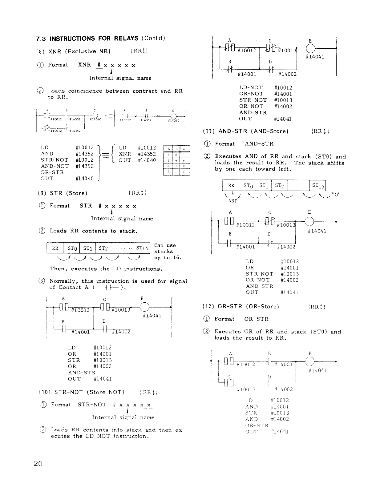
INSTRUCTIONS FOR RELAYS (Cent’d )
XNR (Exclusive NR)
Fc,rmat
Leads coincidence between contract and RR
to RR.
L12
AND
ST R- NOT #10012
AND-NOT #14352
OF.-STR
OIJT
[9)
STR (Store)
Format STR
@
@ Laads RR contents to stack.
XNR#xx xxx
Internal signal name
#loo12
#14352
J
II
f
D
]-i
#140 40
J
#xx
———
Internal signal name
4
{RR$)
LD
XNR #14352
OUT #14040
xxx
#loo12
{RR$I
EIiiElz’1I “2 i-b’”] :::e
E
llp to 16.
I
“.J4’G-’J”J ‘---+
Then, executes the LD instructions.
@ Normally, this instruction is used for signal
of Contact A ( ~ & ) .
A
c
W**
I‘i,,,,o#
LD-NOT
OR-NOT
~T~L-NO’T #10013
OR-NOT
ANI)-STR
o UT
[11 )
AN D-STR (AND-Store)
@ Format A.ND-STR
~~ ~xec~tes AND of RR and stack (s To) and
loads the result to RR. The stack shifts
by one each toward left.
~T~~l
f / ‘e’ ~ti u ~“o’r
.AND’
I
A
~k,,wtl
1
I + } /)14001 -
LD
OR
ST R-NOT #1001?
OR-NOT
AND-STR
OUT
[12 GR-STR [OR-Store)
#loo12
#14001
#14002
#14041
{RR$}
-
I
I
E
-c_
//14041
RR;!
c
#loo131
D
II
‘f{
#14002
#loo12
#14001
#14002
#14041
LD
OR
STR
OR
A.ND-STR
OUT #14041
(10) ST R-NOT (Store NOT)
‘~ Format
@ Loads RR contents
ecutes the LD NOT instruction .
#loo12
#14001
#loo13
#14002
ST R-NOT # X x X x X
20
IRR$;
into stack and then ex—
Format
Executes OR of RR and stack (S TO) and
loads the result to RR.
OIR-STR
~
L]> #loo12
AND
S’rx #loo] 3
.AND
!QR–~TR
C)LT
El
?#i4001
#~4002
314041
E
(13) OUT
{RR–I
(2) TMR (Variable Timer) {RR time up = 1]
@ Format OtJT#xx xxx
I
Internal signal name
@ Writes operation result (RR) to relay.
LD
AN.D
OUT
#loo12
#14001
#14041
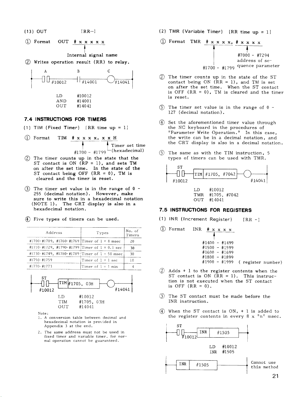
7.4 INSTRUCTIC)NS FOR TIMERS
(1 )
TIM (Fixed Timer) [ RR time
Format
The timer counts up in the state that the
ST contact is ON (RP = 1) , and sets TM
on after the set time.
ST contact being OFF (RR = O) , TM is
cleared and the timer is reset.
@ The timer set value is in the range of O -
255 (decimal notation ) .
su”re to write this in a hexadecimal notation
(NOTE 1).
hexadecimal notation.
TIM#xxxx, xxH
~-—
#1700 - !+1799
In the state of the
The CRT display is also in a
Up=l}
‘~mer set time
~(hexadecimal)
However, make
@ Format
TMR#xxxx, #x xxx
f
#7000 - #7294
I
#1700 - #1799 q
The timer counts up in the state of the ST
contact being ON (RR = 1) , and TM is set
on after the set time,
is OFF (RR = O) , TM is cleared and the timer
is reset.
The timer set value is in the range of O 127 (decimal notation) .
Set the aforementioned timer value through
the NC keyboard in the procedures of
I!parameter Write Operation. “
the write can be in a decimal notation, and
the CRT display is also in a decimal notation.
The same as with the TIM instruction, 5
@
types of timers can be used with TMR.
ST
TIM //1705, //7042
b~ 4
#loo12
LD
TMR #1705, #7042
OUT #14041
7.5
INSTRUCTIONS FOR REGISTERS
#loo12
address of se–
uence parameter
When the ST contact
In this case,
#14041
‘
@ Five types c,f timers can be used.
#1700-#1709,#1760-#1769 Timer of 1 = 8 msec
#1710-#1729,#1790-#1799,Timerof 1 = O.1 sec
==’=e=f!5
#1730-#1749,#1780-#1789ITlmerof 1 = 50 msec 30
#17’30- #1759 Tmer of 1 = 1 sec I 10
#1770 -#1773
—-~- -—
..—
LD #loo12
TIM
OLJT
Note:
1. A conversion table between decimal and
hexadecimal notation is prot ided in
Appendix 3 at the end.
2. The same address must not be used in
fixedtimerand variabletimer, for nor-
operation cannot ‘be guaranteed.
mal
/Timer of 1 = 1 min
#1705, 03H
#14041
4
(1)
INR (Increment Register)
Format
@
Adds + 1 to the register contents when the
ST contact is ON (RR = 1) .
tion is not executed when the ST contact
is OFF (RR = O).
The ST contact must be made before the
3
INR instruction.
When the ST contact is ON, + 1 is added to
the register contents in every 8 x “n” msec.
I
I
INR#x xxx
#1400 - #1499
#1500 - #1599
#1600 - #1699
#1800 - #1899
#1900 - #1999 ( register number)
LD
#loo12
INR #1505
(RR -j
This instruc-
Cannot use
this method
21
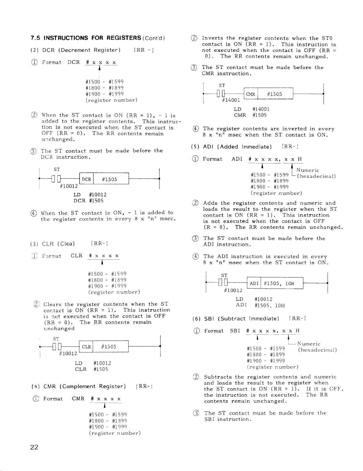
7.5 INSTRUCTIONS FOR REGISTERS [Con!’d )
DCR (Decrement Register)
Format I)CR # x x x x
~ ––
#1500 -
#1599
#1800 - #1899
#1900 - #1999
(register number)
W’hen the ST contact is C)N (RR = 1), - ] is
added to the register contents.
tion is not executed when the ST contact is
OFF (RR = 0).
u:~changed.
The ST contact must be made before the
D(;R instruction.
LD
DCFt #1505
The RR contents remain
#loo12
@ W!~en the ST contact is ON, -1 is added to
the register cclntents in every 8 x “n” msec.
/RR–j
This instruc-
Inverts the register contents when the STO
contact is ON (RR = 1) . This instruction is
not executed when the contact is OFF (RR =
The ST contact must be made before the
CMR instruction.
‘I’he RFL contents remain unchanged .
o).
ST
I
LD
CMR #1505
The
register contents are inverted
8x
AD I
Format
msec. when the ST contact
“n”
(Added Immediate)
AD:[#xxxx, xxH
#14001
_.~ ---
#1500 - #1599
#1800 - #1899
— I
IRR–;
N’umeric
r
(hexadecimal)
in every
is ON.
#1900 - #1999
(register number)
Adds the register contents and numeric and
loads the result to the ~egister when the ST
contact is ON (RR = 1) . This instruction
is not executed when the contact is OFF
(R= O).
The RR contents remain unchanged.
(3’ICLF{ (Clea)
F2r.mat
r
>/
CLR#x xxx
{RR– \
i
#1500 - #1599
#1800 - #1899
#1900 - #1999
(register number)
~ Clears the register contents when the ST
cor.tact is ON (RR = 1).
This instruction
is aot executed when the contact is OFF
The RR contents remain
(RI?.=
o).
unchanged
LD
CL]?. #1505
(4) CMR (Complement Register)
@ Format CMR
#loo12
#x Xxx
{
RR- \
A
#1500 - ?/1599
#1800 - #1899
#1900 - #199~
(register number)
The
ST contact must be macle before the
ADI
instruction.
ADI instruction is executed in every
The
msec when the ST contact is ON.
“n”
8X
ST
r
~D- ;
1
AD I ~ #1505,
{/10012 ‘
LD
#loo12
‘=+
ADI #1505, iOH
(
S3! (Subtract [mmediate)
Format SBI#xxx x,x XH
_ -i—- – --1---
#i500 - #1599
#~80() - #1899
RR- j
— Numeric
(hexadecimal)
#1900 - #1999
(register numi>er)
Subtracts the register contents and numeric
and loads the result to the register when
the ST contact is ON (RR = i) .
the instruction is not executed.
contents remain unchanged.
If it is OFF,
The RR
The ST contact must be made before the
!5BI instruction.
22
H===--+
LD #loo12
AD I
The SB1 instruction is executed in every
8 x “n” msec when the ST contact is ON.
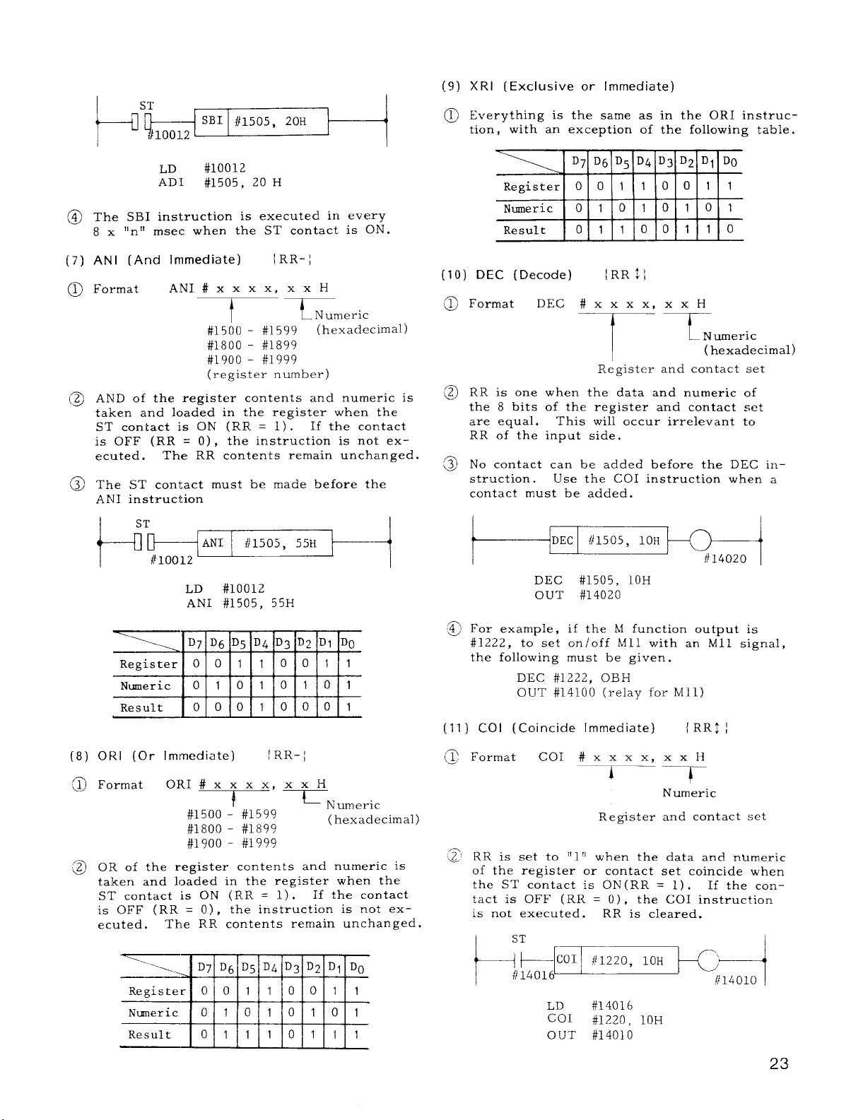
AN I (And Immediate)
Format
AND of the register contents and numeric is
taken and loaded in the register when the
ST contact is ON (RR = 1) . If the contact
is OFF (RR = O) , the instruction is not ex–
ecuted.
The ST contact must be made before the
AN I instruction
#1505, 20 H
I
RR-/
ANI#xxxx, xxH
Numeric
t
#1500 - #1599
#1800 - #1899
#1900 - #1999
(register number)
The RR contents remain unchanged.
t
(hexadecimal)
XRI (Exclusive or [mmediate)
(9)
Everything is the same as in the ORI instruc-
@
(10) DEC (Decode)
with an exception of the following table.
tion,
D7 Dfj D5 D4 D3 D2 D1 DO
Register
Numeric
Result
Format
RR is one when the data and numeric of
the 8 bits of the register and contact set
are equal.
RR of the input side.
No contact can be added before the DEC instruction. Use the CO I instruction when a
contact must be added.
o 0 1 1 0 0 1 1
o 1 0 1 0 1 0 1
o 1 1 0 0 1 1 0
{RR$I
DE C#xxxx, xxH
-~~:,,,,cimal)
Register and contact set
This will occur irrelevant to
Hd==--l
LD #10012
ANI #1505, 55H
D7 D6 D5 D4 D3 D2 D1 Do
Register
Numeric
Result
OR I (Or Immediate)
Format ORI#xxxx, xxH
01{ of the register contents and numeric is
taken and loaded in the register when the
ST contact is ON (RR = 1) . If the contact
is OFF (RR = O) , the instruction is not executed.
\
“-=..
Register
Numeric o 1 0 1 0 1 0 1
Result o 1 1 1 0 1 1 1
o 0 1
o 1 0 1 0 1 0 1
o 0 0 1 0 0 0 1
#1500 - #1599
#1800 - #1899
#1900 - #1999
The RR contents remain unchanged.
DJ D(5 D5 D4 D3 D2 D1 Do
o ‘o 1 1 ‘o o 1 1
1 0 0 1 1
{
RR– ;
I
L-
Numeric
( hexadecimal)
b
For example, if the M function output is
#1222, to set ori/off Mll with an Mll signal,
the following must be given.
(11 )
CO I (Coincide Immediate)
Format
RR is set to 11111when the data and numeric
of the register or contact set coincide when
the ST contact is ON(RR = 1) .
tact is OFF (RR = O) , the COI instruction
is not executed.
DEC {/1505, 10H
DEC #1505, 10H
OUT #14020
DEC #1222, OBH
OUT #14100 (relay for Mll)
{RR$ !
COI#xxxx, xxH
“-~ ._T
Numeric
Register and contact set
If the con-
RR is cleared.
ST
+
~CO1l #1220, 10H ; ‘
;!14016
LD
COI
OUT #14010
#14016
#1220, 10H
~v
6t
I
#14010
23

7.5 INSTRUCTIONS FOR REGISTERS ( Cent’d )
(12) CMP (Compare)
Format
@
@ If the comparison result of the 8-bit data
and numeric of the register and contact set
is that the register (contact set) is equal or
greater than the numeric, RR is set to ‘i1. ‘1
If the register ( contact set) is smaller than
the numeric, “RR is cleared.
ed irrelevant to RR of the input side,
@ No contact can be added before the CMP in-
struction.
contact must be added.
CMP#xxxx, xxH
Use the CPI instruction when a
+-.+fF, #1230, li)H~---j
I
#1230 2 10H
#1230 <
10H
CMP
OIJT
[13) CPI (Compare Immediate)
~ Format
RR is set to
of the data and numeric of the register or
contact set is that the register (contact
set) is greater or equal to the numeric
when the ST contact is ON (RR = 1) .
When the ST contact is OFF (RR = 1) , the
!CPI instruction is not executed.
cleared.
CPI#xxxx, xxH
‘~--- ~N~eric
{RR$;
~7
Register and contact set
~-. Numeric
(hexadecimal)
This is execut-
/)14500 I
+Z1=ON
+ 21 = OFF
#1230, IOH
#14500
{
RR$)
(hexadecimal)
Re@ster and contact set
I!l!! if the comparison resuit
RR is
This instruction transfers the numeric to
@
the register when the ST contact is ON
(RR = 1).
the MVI instruction is not (executed.
RR is not affected by the MVI instruction.
3
If the ST
‘a
If the contact is OFF (RR = O) ,
LD
#14002
MVI #1505, 15H
cc,ntactis ON, the MV1 instruction
is executed in every 8 x “n !!msec.
(15:
ADD (ADD Register) { P.R– j
‘3
Format
ADD#xxxx, #xxx
TT
Operating register (Rl )
Register to be
operated (R2)
When the ST contact is OIi (RR = 1) , the
register (R2) contents and register (Rl)
are added and the result is loaded in
register (R2) ,
remain unchanged.
remain unchanged.
not executed when the ST contact is OFF
(RR =
0).
The R1 register contents
The RR contents also
The ADD instructions
j—sr~~mm=i+:
LD
//14012
AD12 #1501, #1502
Note:
underflow is not performed.
result less than 255 (FFH) ; with SUB, do not
make RI >R2.
(16)
@ Everything is the same as the ADD in-
In ADD cm SLIB, detecticm of overflow or
With ADD , make the
SUB (Sub !?egister) ; R“X-;
struction ,
except here the operation is
subtraction (R2-R1 ~ R2) ,
I
LD
CPI
0 UT
(14)
LIVI (Move Immediate] i XR-;
~ Format
MVI#xxxx, xxH
#14002
#1~30, 10H
#14500
–---T---- ~–.
Register
24
Numeric
(hexadecimal)
[17) ANR {And Register) ! RR– /
‘~ Everything :1s
the same as the ADD in–
struction, except lhere the operation is
AND ,
(18) !IRR (Or Register)
(R2 AND R1 _ R2)
I RR- ;
(Z) Everything is the same as the ADD in-
5tz_uction,
IGR.
except here the operation is
(R2 01< R1 ~
R2)
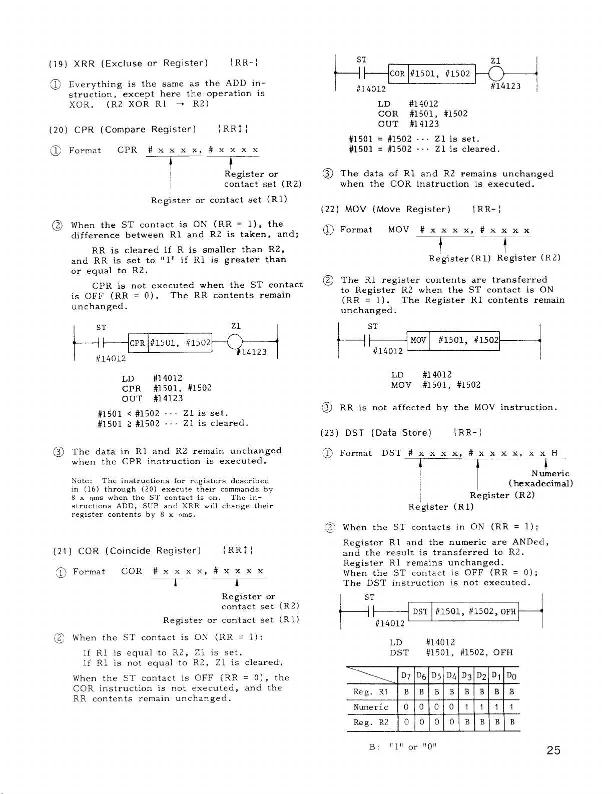
(19) XRR (Excluse or Register)
~ Everything is the same as the ADD in-
struction, except here the operation is
XOR. (R2 XOR R1 ~ R2)
(20) CPR (Compare Register)
~ Format
@ When the ST contact is ON (RR = 1), the
difference between R1 and R2 is taken, and;
and RR is set to
or equal to R2.
is OFF (RR = O).
unchanged.
CPR#xxxx, #x xxx
Register or contact set (RI)
RR is cleared if R is smaller than R2,
“1“ if R1 is greater than
CPR is not executed when the ST contact
The RR contents remain
[RR-!
{RR~~
1
Register or
contact set (R2)
Z1
+s;
I
{/14012
#1501 ~ #1502 . . . Z1 is set.
#1501 2 #1502 “~. Z1 k cleared.
CPR #1501, /}1502
LD
CPR #1501, #1502
OUT #14123
#14012
ST
COR #1501, #1502
p~ ~
#14012
LD
COR #1501, #1502
OUT #14123
#1501 = #1502 . . . Z1 is set.
#1501 = #1502 . . . Z1 is cleared.
@ The data of R1 and R2 remains unchanged
when the COR instruction is executed.
(22)
MOV (Move Register)
@ Format
@ The R1 register contents are transferred
to Register R2 when the ST contact is ON
(RR = 1). The Register R1 contents remain
unchanged.
(t
l.;~__._l
@ RR is not affected by the MOV instruction.
(23)
DST (Data Store) {RR-]
#14012
MOV#xxxx, #x xxx
_l_ –T.
Register (Rl) Register (Rz)
LD
MOV #1501, #1502
#14012
zl
//14123
{RR- I
@ The data in R1 and R2 remain unchanged
when the CPR instruction is executed.
Note:
in
8 x nms when tbe ST contactis on.
structionsADD, SUB and XRR willchange their
The instructions for registers described
(16)through (20)executetheircommands by
The in-
registercontentsby 8 x rims.
(21 ) COR (Coirlcide Register)
@ Format
CO R#xxxx, #xxx x
—-T- --~-–.
{RR$}
Register or
contact set (R2)
Register or contact set (Rl)
@ When the ST contact is ON (RR = 1):
If R1 is equal to R2, Z1 is set.
If R1 is not equal to R2, Z1 is cleared,
When the ST contact is OFF (RR = 0) , the
COR instruction is not executed, and the
RR contents remain unchanged.
@Format DST#x xxx, #xxx x,xx H
~~he-:)
I
Register (Rl)
~ When the ST contacts in ON (RR = 1) ;
Register R1 and the numeric are ANDed.
an; the result is transferred to R2.
Register R1 remains unchanged.
When the ST contact is OFF (RR = O) ;
The DST instruction is not executed.
I
Al
//14012
DST #1501, #1502, OFH1
LD
DST
#14012
#1501, #1502, OFH
Register (R2)
,
D7 D6 D5 D4 D3 D2D1DO
RI
Reg.
Numeric
Reg. R2 o 0 0 0 B
B B B B B B
o 0 c o 1
B B
1 1 1
B B B
B:
11111 or 1! 01!
25
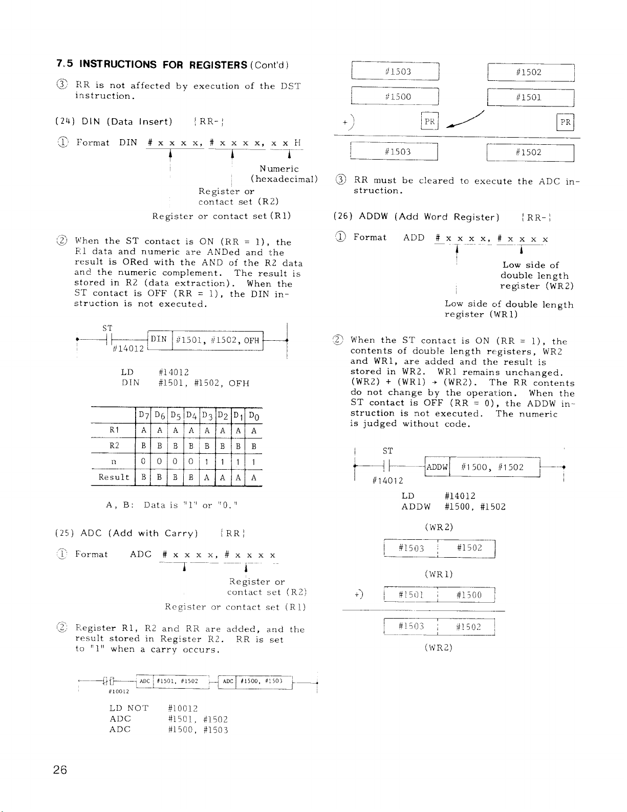
7.5 INSTRUCTIONS FOR REGISTERS (Cent’d )
@’ RR is not affected by execution of the DST
instruction.
DIN (Data Insert)
(24)
‘~ ’Format DIN#x xxx, #xxx x,xx H
~> When the ST contact is ON (RR = 1), the
F.1 data and numeric are ANDed and the
result is ORed with the Ah’D of the R2 data
and the numeric complement .
stored in R2 (data extraction) .
ST contact is OFF (RR = 1) , the DIN in-
struction is not executed.
ST
~-—-. }— DIN #l~ol, 7}1502,OFH
~ .–r- – ----
Register or contact set (Rl)
{R R-I
Nurne~ic-
(hexadecimal)
Register or
contact set (R2)
The result is
When the
1
//14012I
LD
DIN
RI A A A A A
R2
n
Result
#14012
#1501, #1502, OFH
D7 Dfj D5 D4 D3
B- B B B B
0 0 0 0’ 1
B B B B A
D2 D, Do
1A
A A
B B B
1 1 1
A A A
PR
n
~———
LI!2!!2
@ RR must be cleared to execute the ADC in-
struction.
(26)
ADDW (Add Word Register)
@ Format
,-
When the ST contact is ON (RR = 1), the
2’
‘.J’
contents of ciou’blelength registers , WR2
and WR1, are added and the result is
stored in WR2.
(WR2) + (WR1) + (WR2) . The RR contents
do not change by the operation.
ST contact is OFF (RR = O) , the ADDW instruction is not executed.
is judged without code.
3
AD D#xxxx, #x xxx
Low side c,f double length
register (WR1)
WR1 remains unchanged.
~~]
{ RR– \
side of
Low
double length
register (WR2)
When the
The numeric
t+j- 1500, //1502 ~;
A, B:
(25) ADC (Add with Carry)
~ Format
~~ llegisterR1 ,
result stored in Register R2.
tO “l” when a carry occurs.
!-–+~z)c ~#lSol, #,502
I1OO12
LD NOT
ADC
ADC #1500, /41503
Data is “l” or “O.”
‘Dc !..+..X “ # x ~x-.x‘_
Register or contact set (Rl)
R2 and RR are added, and the
-.—_+zEIzEzE3
++10012
#1501, +l~o~
26
{RR I
Register or
contact set (R2)
R.R is set
LD
ADDW #1500, #1502
#14012
(WR2)
.
 Loading...