

Yamaha MG16, MG16XU Service Manual
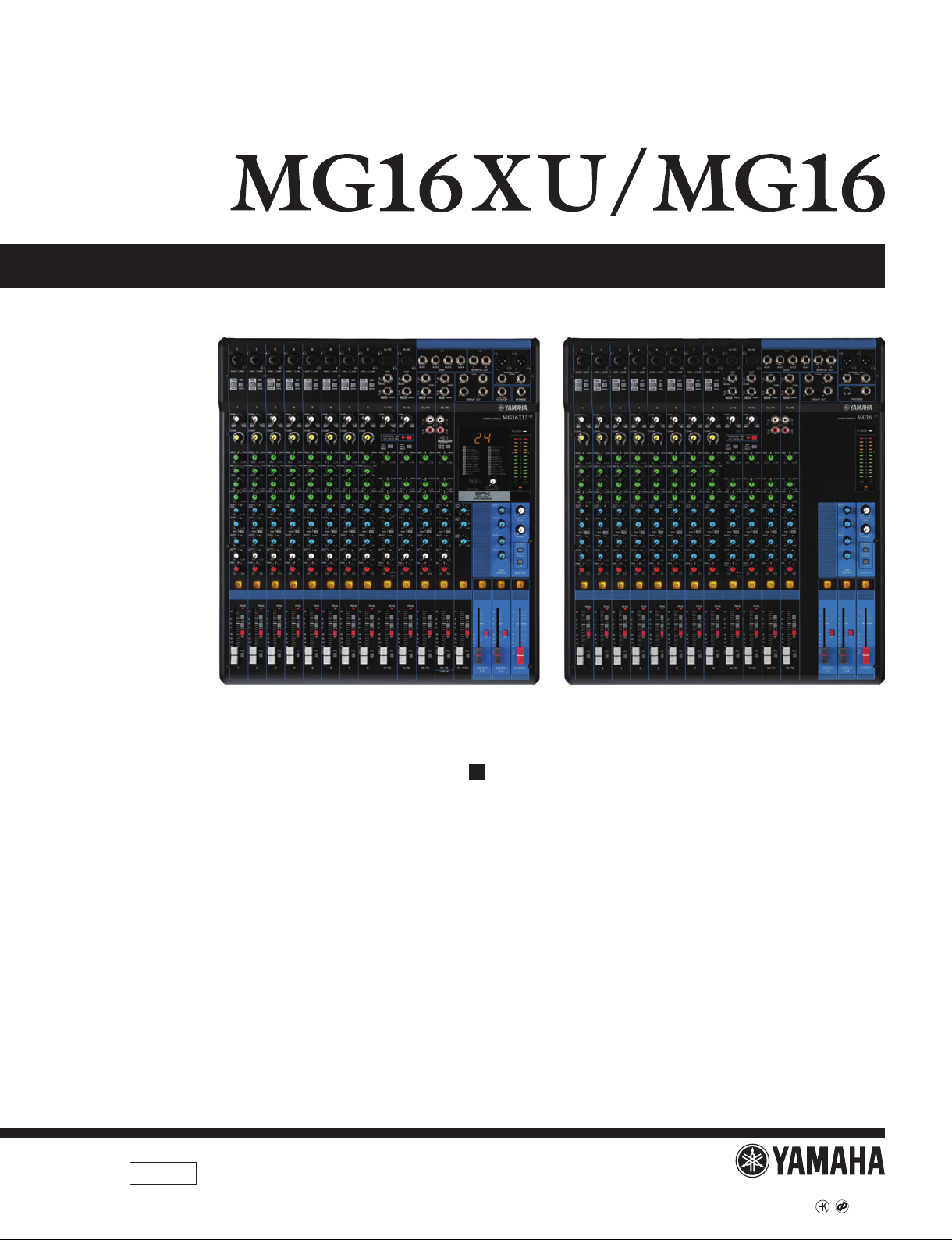
MIXING CONSOLE
SERVICE MANUAL
SERVICE MANUAL
MG16XU MG16
CONTENTS (目次)
SPECIFICATIONS(総合仕様) ................................3/5
DIMENSIONS(寸法図) ..............................................7
PANEL LAYOUT(パネルレイアウト) .......................8
CIRCUIT BOARD LAYOUT & WIRING
(ユニットレイアウト & 結線図) .............................10
DISASSEMBLY PROCEDURE(分解手順) .............12
LSI PIN DESCRIPTION(LSI 端子機能表) ...............28
CIRCUIT BOARDS(シート基板図) .........................30
INSPECTIONS(検査) ..............................................40
RACK MOUNTING(ラックマウント) ................59/60
PARTS LIST
BLOCK & LEVEL DIAGRAM
(ブロック&レベルダイアグラム)
CIRCUIT DIAGRAM(回路図)
PA
012118
HAMAMATSU, JAPAN
Copyright (c) Yamaha Corporation. All rights reserved. PDF ’14.04
MG16XU/MG16
IMPORTANT NOTICE
This manual has been provided for the use of authorized Yamaha Retailers and their service personnel. It has been assumed that basic
service procedures inherent to the industry, and more specifically Yamaha Products, are already known and understood by the users,
and have therefore not been restated.
WARNING : Failure to follow appropriate service and safety procedures when servicing this product may result in personal injury,
IMPORTANT : This presentation or sale of this manual to any individual or firm does not constitute authorization certification,
The data provided is belived to be accurate and applicable to the unit(s) indicated on the cover. The research engineering, and service
departments of Yamaha are continually striving to improve Yamaha products. Modifications are, therefore, inevitable and changes in
specification are subject to change without notice or obligation to retrofit. Should any discrepancy appear to exist, please contact the
distributor’s Service Division.
WARNING : Static discharges can destroy expensive components. Discharge any static electricity your body may have accumulated
destruction of expensive components and failure of the product to perform as specified. For these reasons, we advise
all Yamaha product owners that all service required should be performed by an authorized Yamaha Retailer or the
appointed service representative.
recognition of any applicable technical capabilities, or establish a principal-agent relationship of any form.
by grounding yourself to the ground bus in the unit (heavy gauge black wires connect to this bus.)
IMPORTANT : Turn the unit OFF during disassembly and parts replacement. Recheck all work before you apply power to the unit.
WARNING: This product contains chemicals known to the State of California to cause cancer, or birth defects or other reproductive harm.
DO NOT PLACE SOLDER, ELECTRICAL/ELECTRONIC OR PLASTIC COMPONENTS IN YOUR MOUTH FOR ANY REASON WHAT SO EVER!
Avoid prolonged, unprotected contact between solder and your skin! When soldering, do not inhale solder fumes or expose eyes to solder/
flux vapor!
If you come in contact with solder or components located inside the enclosure of this product, wash your hands before handling food.
WARNING
Components having special characteristics are marked and must be replaced with parts having specification equal to those
originally installed.
印の商品は、安全を維持するために重要な部品です。交換する場合は、安全のために必ず指定の部品をご使用ください。
2
SPECIFICATIONS
MG16XU/MG16
General Specifications
Frequency Response
Total Harmonic Distortion
(THD+N)
Hum & Noise *1
(20 Hz to 20 kHz)
Crosstalk (1kHz) *2
Bus STEREO: 1, GROUP: 4, AUX: 4 (MG16XU: incl. FX)
Input Channel Function PAD CH 1 – CH 8 26 dB
Level Meter
Built-in Effect (MG16XU)
USB Audio (MG16XU) 2 IN / 2 OUT
Phantom Power Voltage +48 V
Power Requirements AC 100-240 V, 50 Hz/60 Hz
Power Consumption 30 W
Dimensions (W × H × D) 444 mm × 130 mm × 500 mm (17.5" × 5.1" × 19.7")
Net Weight MG16XU: 6.8 kg (15.0 lbs.), MG16: 6.6 kg (14.6 lbs.)
Included Accessory
Optional Accessory Foot Switch: FC5 (MG16XU)
Operating Temperature 0 to +40 °C
*1 Noise is measured with A-weighting filter.
*2 Crosstalk is measured with 1 kHz band pass filter.
Input to STEREO OUT +0.5 dB/-1.5 dB (20 Hz to 48 kHz) ,
refer to the nominal output level @ 1 kHz, GAIN knob: Min
Input to STEREO OUT 0.03 %@ +14 dBu (20 Hz to 20 kHz), GAIN knob: Min
0.005 %@ +24 dBu (1 kHz), GAIN knob: Min
Equivalent Input Noise -128 dBu (Mono Input Channel, Rs: 150 Ω, GAIN knob: Max)
Residual Output Noise -102 dBu (STEREO OUT, STEREO master fader: Min)
-78 dB
16 channels: Mono [MIC/LINE]: 8, Mono/Stereo [MIC/LINE]: 2, Stereo [LINE]: 2Input channels
STEREO OUT: 2, PHONES: 1, MONITOR OUT: 1, AUX SEND: 4, GROUP OUT: 4Output channels
HPF CH 1 – CH 8,
CH 9/10 (MIC),
CH 11/12 (MIC)
COMP CH 1 – CH 8 1 knob compressor (Gain/Threshold/Ratio)
EQ CH 1 – CH 8 HIGH:Gain: +15 dB/-15 dB, Frequency: 10 kHz shelving
CH 9/10 –
CH 15/16
PEAK LED CH 1 – CH 11/12
Pre Monitor LEVEL 2 × 12 -segment LED meter [PEAK, +10, +6, +3, 0, -3, -6, -10, -15, -20, -25, -30 dB]
SPX Algorithm 24 programs, PARAMETER control: 1, FOOT SW: 1 (FX RTN CH on/off)
USB Audio Class 2.0 compliant, Sampling Frequency: Max 192 kHz, Bit Depth: 24-bit
AC power cord, Rack mount kit, Cubase AI Download Information (MG16XU),
Owner’s Manual, Technical Specifications
0 dBu = 0.775 Vrms Output impedance of signal generator (Rs) = 150Ω
80 Hz, 12 dB/oct
Threshold: +22 dBu to -8 dBu, Ratio: 1:1 to 4:1,
Output level: 0 dB to 7 dB, Attack time: approx. 25 msec,
Release time: approx. 300 msec
MID:Gain: +15 dB/-15 dB, Frequency: 250 Hz to 5 kHz peaking
LOW:Gain: +15 dB/-15 dB, Frequency: 100 Hz shelving
HIGH:Gain: +15 dB/-15 dB, Frequency: 10 kHz shelving
MID:Gain: +15 dB/-15 dB, Frequency: 2.5 kHz peaking
LOW:Gain: +15 dB/-15 dB, Frequency: 100 Hz shelving
LED turns on when post EQ signal reaches 3 dB below clipping level
European Models :
Inrush Current based on EN 55103-1:2009
3.0 A (on initial switch-on)
2.0 A (after a supply interruption of 5s)
Conforms to Environments: E1, E2, E3 and E4
Analog Input Characteristics
Input Jacks
MIC/LINE
1 - 8
MIC
9/10, 11/12
LINE
9/10, 11/12
LINE
13/14, 15/16
PAD
26 dB
OFF
ON
—
—
— —
GAIN Trim
Position
+64 dB
+20 dB
+38 dB
-6 dB
+64 dB
+20 dB
+38 dB
-6 dB
Actual Load
Impedance
3 kΩ
3 kΩ
10 kΩ
10 kΩ
For Use With
Nominal
50–600 Ω
Mics/Lines
50–600 Ω
Mic
600 Ω
Lines
600 Ω
Lines
Sensitivity
-80 dBu
(0.077 mV)
-36 dBu
(12.3 mV)
-54 dBu
(1.55 mV)
-10 dBu
(245 mV)
-80 dBu
(0.077 mV)
-36 dBu
(12.3 mV)
-54 dBu
(1.55 mV)
-10 dBu
(245 mV)
-30 dBu
(24.5 mV)
Input level
*1
Nominal Max. before clip
-60 dBu
(0.775 mV)
-16 dBu
(122.8 mV)
-34 dBu
(15.46 mV)
+10 dBu
(2.451 V)
-60 dBu
(0.775 mV)
-16 dBu
(122.8 mV)
-34 dBu
(15.46 mV)
+10 dBu
(2.451 V)
-10 dBu
(245 mV)
All level knobs are nominal if not specified.
Balanced /
Unbalanced
Balanced
Balanced
Unbalanced
Unbalanced
-40 dBu
(7.75 mV)
+4 dBu
(1.228 V)
-14 dBu
(154.6 mV)
+30 dBu
(24.51 V)
-40 dBu
(7.75 mV)
-6 dBu
(389 mV)
-14 dBu
(154.6 mV)
+30 dBu
(24.51 V)
+10 dBu
(2.45 V)
Jack
XLR-3-31*2
TRS PHONE
(6.3 mm)*3
Combo type
XLR-3-31*2
TRS PHONE
(6.3 mm)*4
TRS PHONE
(6.3 mm)*4
RCA PIN
3
MG16XU/MG16
Analog Output Characteristics
Output Terminals
STEREO OUT L, R
MONITOR OUT L, R
GROUP OUT 1–4
AUX SEND 1–4
PHONES
0 dBu is referenced to 0.775 Vrms.
*1 Sensitivity is the lowest level that will produce an output of +4dBu (1.228V) or the nominal output level when the unit is set to maximum gain.
(All level controls are maximum position.)
*2 1&Sleeve=GND, 2&Tip=HOT, 3&Ring=COLD
*3 Tip=HOT, Ring=COLD, Sleeve=GND
*4 Tip=Signal, Ring=GND, Sleeve=GND
*5 Tip=LEFT, Ring=RIGHT, Sleeve=GND
Actual Source
Impedance
75 Ω 600 Ω Lines
150 Ω 10k Ω Lines
110 Ω
With Nominal
40 Ω Phones
For Use
Output level
Nominal
+4 dBu
(1.228 V)
+4 dBu
(1.228 V)
3 mW + 3 mW
Max.
before clip
+24 dBu
(12.28 V)
+20 dBu
(7.750 V)
100 mW + 100 mW
Jack
*2
XLR-3-32
TRS Phone(6.3mm)
TRS Phone(6.3mm)*3
Stereo Phone Jack
Balanced / Unbalanced /
Impedance Balanced
*3
*5
Balanced
Impedance
Balanced
—
Digital Input / Output Characteristics (MG16XU)
Terminals Forma t Data length Fs Connector
USB
Data length depends on the particular audio format being used. USB Audio Class 2.0: 16-bit/24-bit, Yamaha Steinberg USB Driver: 24-bit
USB Audio Class 2.0
16-bit/24-bit
44.1 kHz, 48 kHz, 88.2 kHz, 96 kHz, 176.4 kHz, 192 kHz
USB Standard-B
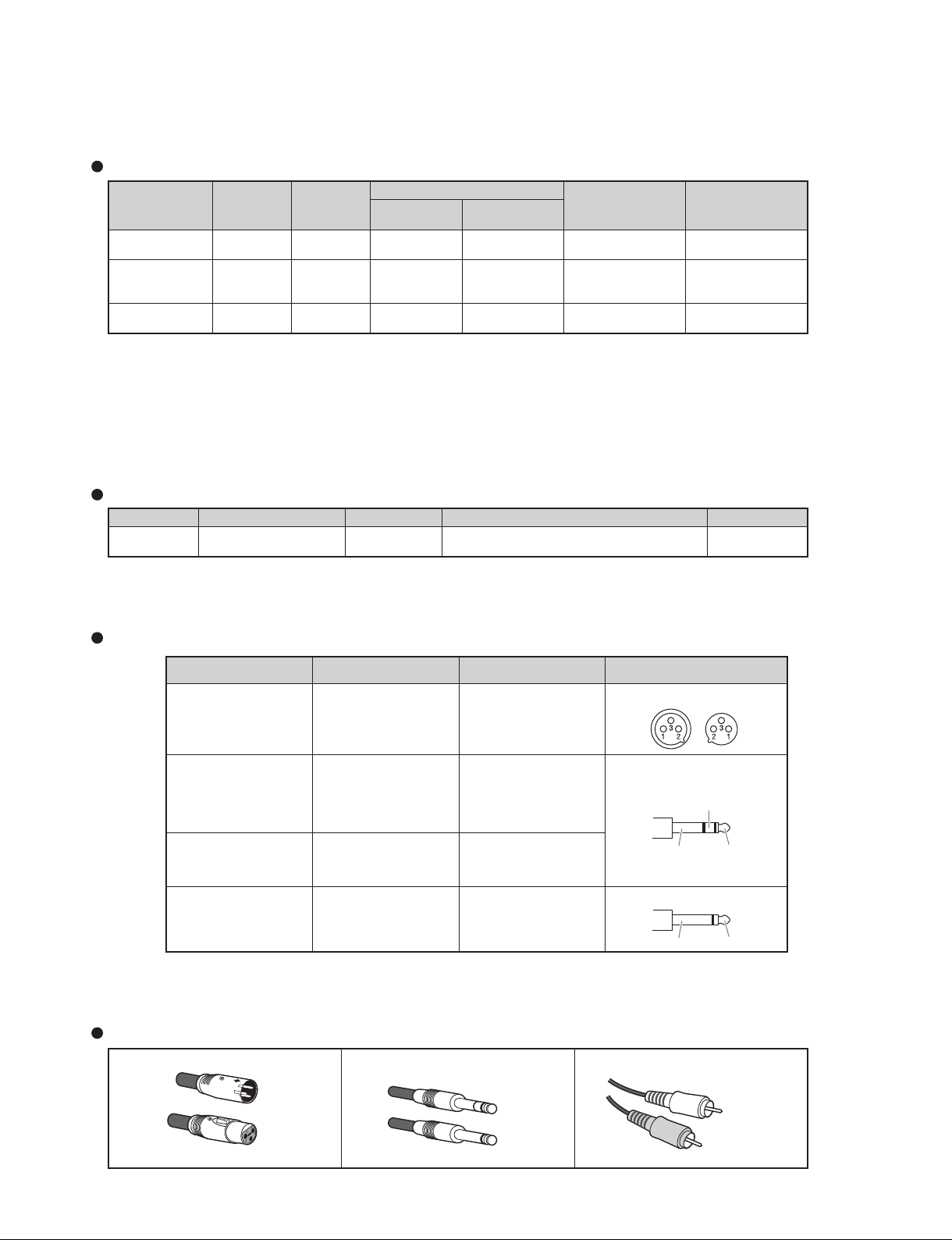
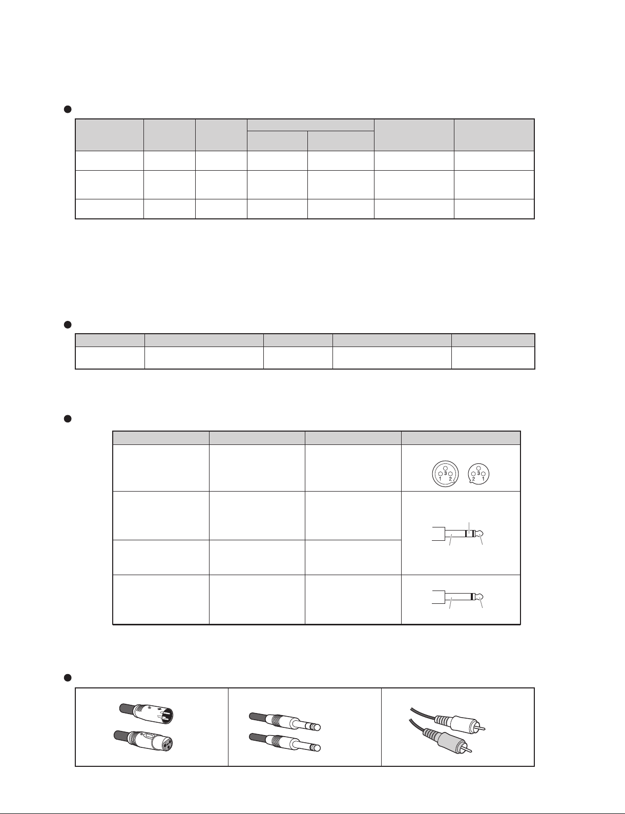
Jack and Connector List (Pin Alignment)
Jacks and Connectors Polarities Balanced/Unbalanced Configurations
MIC/LINE
MIC
STEREO OUT
MIC/LINE*
AUX SEND*
GROUP OUT*
STEREO OUT*
MONITOR OUT*
PHONES
LINE
(stereo input Channels)
* These jacks also can be connected with TS phone connectors. If you use TS phone connectors, the connection will be unbalanced.
Pin 1: Ground
Pin 2: Hot (+)
Pin 3: Cold (-)
Tip: Hot (+)
Ring: Cold (-)
Sleeve: Ground
Tip: L
Ring: R
Sleeve: Ground
Tip: Hot
Sleeve: Ground
Balanced
Balanced
—
Unbalanced
XLR connector
TRS phone plug
Ring
TS phone plug
OUTPUTINPUT
TipSleeve
TipSleeve
Connector Types
XLR Phone RCA Pin
Male
Female
TRS Phone
TS Phone
L (White)
R (Red)
4

総合仕様
MG16XU/MG16
一般仕様
周波数特性
全高調波歪率(TH D+N) 入力チャンネル
ハム&ノイズ
(20Hz〜20kHz)
クロストーク(1kHz)
入力チャンネル モノラル(MIC/LINE):8 、モノラル/ステレオ(MIC/LINE):2、ステレオ(LINE):2
出力チャンネル
バス
入力チャンネル機能 PAD
Level Meter
Built-in Effect (MG16XU)
USB Audio (MG16XU)
Phantom Power Voltage
Power Requirements
Power Consumption
Dimensions (W × H × D)
Net Weight
Included Accessory
Optional Accessory
Operating Temperature
*1:ノイズはA-weightingフィルターで測定。
*2:1kHzバンドパスフィルターで測定。
*1
*2
入力チャンネル
→STEREOOUT
→STEREOOUT
入力換算ノイズ
出力残留ノイズ
HPF(ハイパスフィル ター)
COMP
EQ(イコライザー)
PEAKLED
モニターレベル調整前
SPXアルゴリズム
2IN/2OUT
+0.5dB/-1.5dB(20Hz〜48kHz)、
1kHz@ノミナル出力基準、GAINツマミ:最小
0.03%@+14dBu(20Hz〜20kHz)、GAINツマミ:最小
0.005%@+24dBu(1k Hz )、GAINツマミ:最 小
-128dBu(モノラルインプットチャンネル、Rs:150Ω、GAINツマミ:最 大 )
-102dBu(STEREOOUT、STEREOマスターフェーダー:最小)
-78dB
STEREOOUT:2、MONITOROUT:1、PHONES:1、AUXSEND:4、GROUPOUT:4
STEREO
CH 1 – CH 8 26dB
CH 1 – CH 8,
CH 9/10 (MIC),
CH 11/12 (MIC)
CH1‒CH8
CH1‒CH8
CH9/10‒
CH15/16
CH1‒CH11/12
2×12ポイントLEDメーター(PEAK、+10、+6、+3、0、-3、-6、-10、-15、-20、-25、-30dB)
24種類、PARAMETERノブ:1、FOOTSW(フットスイッチ):1(FXRTNチャンネルオン/オフ)
USBAudioClass2.0準拠、対応サンプリング周波数:最大192kHz、対応量子化ビット数:24ビット
+48V
AC100〜240V、50/60Hz
30W
444mm×130mm×500mm
MG16XU:6.8kg、MG16:6.6kg
電源コード、ラックマウント金具、取扱説明書、TechnicalSpecifications、
CUBASEAIDOWNLOADINFORMATION(MG16XUモデル)
フットスイッチ:FC-5(MG16XU)
0〜+40℃
0dBu=0.775Vrmsシグナルジェネレーターの出力インピーダンス:150Ω
特に指定がない場合、ノブやフェーダーの位置は全てノミナル位置です。
:
1、GROUP:4、AUX:4(MG16XU:FX含む)
80Hz、12dB/oc t
1つのノブでパラメーター(ゲイン、スレッショルド、レシオ)を同時に調節
スレッショルド:+22dBu〜-8dBu、レシオ:1:1〜4:1、
出力レベル:0dB〜7dB、アタックタイム:約25msec、リリース
タイム:約300msec
HIGH:ゲイン:+15dB/-15dB、カットオフ周波数:10kHzシェルビング
MID:ゲイン: +15dB/-15dB、中心周波数 : 250Hz〜5kHzピーキング
LOW:ゲイン:+15dB/-15dB、カットオフ周波数:100Hzシェルビング
HIGH:ゲイン:+15dB/-15dB、カットオフ周波数:10kHzシェルビング
MID:ゲイン: +15dB/-15dB、中心周波数 : 2.5kHzピーキング
LOW:ゲイン:+15dB/-15dB、カットオフ周波数:100Hzシェルビング
イコライザー後の信号がクリッピングの手前3dBに達すると点灯
アナログ入力仕様
入力端子名称
MIC/LINE
1-8
MIC
9/10,11/12
LINE
9/10,11/12
LINE
13/14,15/16
PAD
26dB
OFF
ON
10kΩ
ゲイン
+64dB
+20dB
+38dB
-6dB
+64dB
+20dB
+38dB
-6dB
入力イン
ピーダンス
3kΩ
3kΩ
10kΩ
適合イン
ピーダンス
50‒600Ω
Mics/Lines
50‒600Ω
Mic
600Ω
Lines
600Ω
Lines
感度*1 ノミナル
-80dBu
(0.077mV)
-36dBu
(12.3mV)
-54dBu
(1.55mV)
-10dBu
(245mV)
-80dBu
(0.077mV)
-36dBu
(12.3mV)
-54dBu
(1.55mV)
-10dBu
(245mV)
-30dBu
(24.5mV)
入力レベル
-60dBu
(0.775mV)
-16dBu
(122.8mV)
-34dBu
(15.46mV)
+10dBu
(2.451V)
-60dBu
(0.775mV)
-16dBu
(122.8mV)
-34dBu
(15.46mV)
+10dBu
(2.451V)
-10dBu
(245mV)
最大ノンクリッピング
-40dBu
(7.75mV)
+4dBu
(1.228V)
-14dBu
(154.6mV)
+30dBu
(24.51V)
-40dBu
(7.75mV)
-6dBu
(389mV)
-14dBu
(154.6mV)
+30dBu
(24.51V)
+10dBu
(2.45V)
XLR-3-31*2
TRSフォーンジャック
(6.3mm)*3
コンボタイプ
XLR-3-31*2
TRSフォーンジャック
(6.3mm)*4
TRSフォーンジャック
端子仕様
(6.3mm)
RCAピン
バランス型
バランス型
アンバランス型
*4
アンバランス型
バランス/
アンバランス
5
MG16XU/MG16
アナログ出力仕様
出力端子名称
STEREOOUTL,R
MONITOROUTL,R
GROUPOUT1‒4
AUXSEND1‒4
PHONES
0dBu=0.775Vrms
*1 入力感度:最大レベル設定時で+4dB(1.228V)またはノミナルレベルを出力するときに得られる最小レベル(レベルコントロールはすべて最大)。
*2 1&スリーブ=グランド、2&チップ=ホット、3&リング=コールド
*3 チップ=ホット、リング=コールド、スリーブ=グランド
*4 チップ=シグナル、リング=グランド、スリーブ=グランド
*5 チップ=LEFT、リング=RIGHT、スリーブ=グランド
出力イン
ピーダンス適合インピーダンス
75Ω 600ΩLines
150Ω 10kΩLines
110Ω
40ΩPhones
出力レベル
ノミナル
+4dBu
(1.228V)
+4dBu
(1.228V)
3mW+3mW
最大ノン
クリッピング
+24dBu
(12.28V)
+20dBu
(7.750V)
100mW+100mW
端子仕様
XLR-3-32
TRSフォーンジャック(6.3mm)*3
TRSフォーンジャック(6.3mm)
ステレオフォーンジャック
*2
*5
バランス/アンバランス
バランス型
インピー ダンス
*3
バランス型
デジタル入力/出力仕様(MG16XU)
出力端子名称 サンプリング周波数 端子仕様
USB USBオーディオ2.0 16/24bit
データ長は使用されているオーディオ形式に依存します。 USBオーディオ2.0:16/24-bit、YamahaSteinbergUSBドライバー:24-bit
フォーマット データ長*6
44.1kHz,48kHz,88.2kHz,
96kHz,176.4kHz,192kHz
端子の極性(ピン配列)
出力端子名称 端子の極性 バランス/アンバランス 端子の形状
MIC/LINE
MIC
STEREOOUT
MIC/LINE*
AUXSEND*
GROUPOUT*
STEREOOUT*
MONITOROUT*
PHONES
LINE
(
ステレオ入力チャンネル
ピン1: グラウンド
ピン2: ホット(+)
ピン3: コールド(−)
チップ:ホット(+)
リング:コールド(−)
スリーブ:グランド
チップ:L
リング:R
スリーブ:グランド
チップ:ホット
)
スリーブ:グランド
バランス型
バランス型
−
アンバランス型
XLRコネクター
TRSフォーンプラグ
リング
TSフォーンプラグ
USBBタイプ
メスオス
チップスリーブ
チップスリーブ
*アンバランス型のTSフォーンプラグも使用できます。 使用した場合はアンバランス型となります。
コネクターの種類
XLR フォーン RCAピン
オス
メス
TRSフォーン
プラグ
TSフォーン
プラグ
L(白)
R(赤)
6
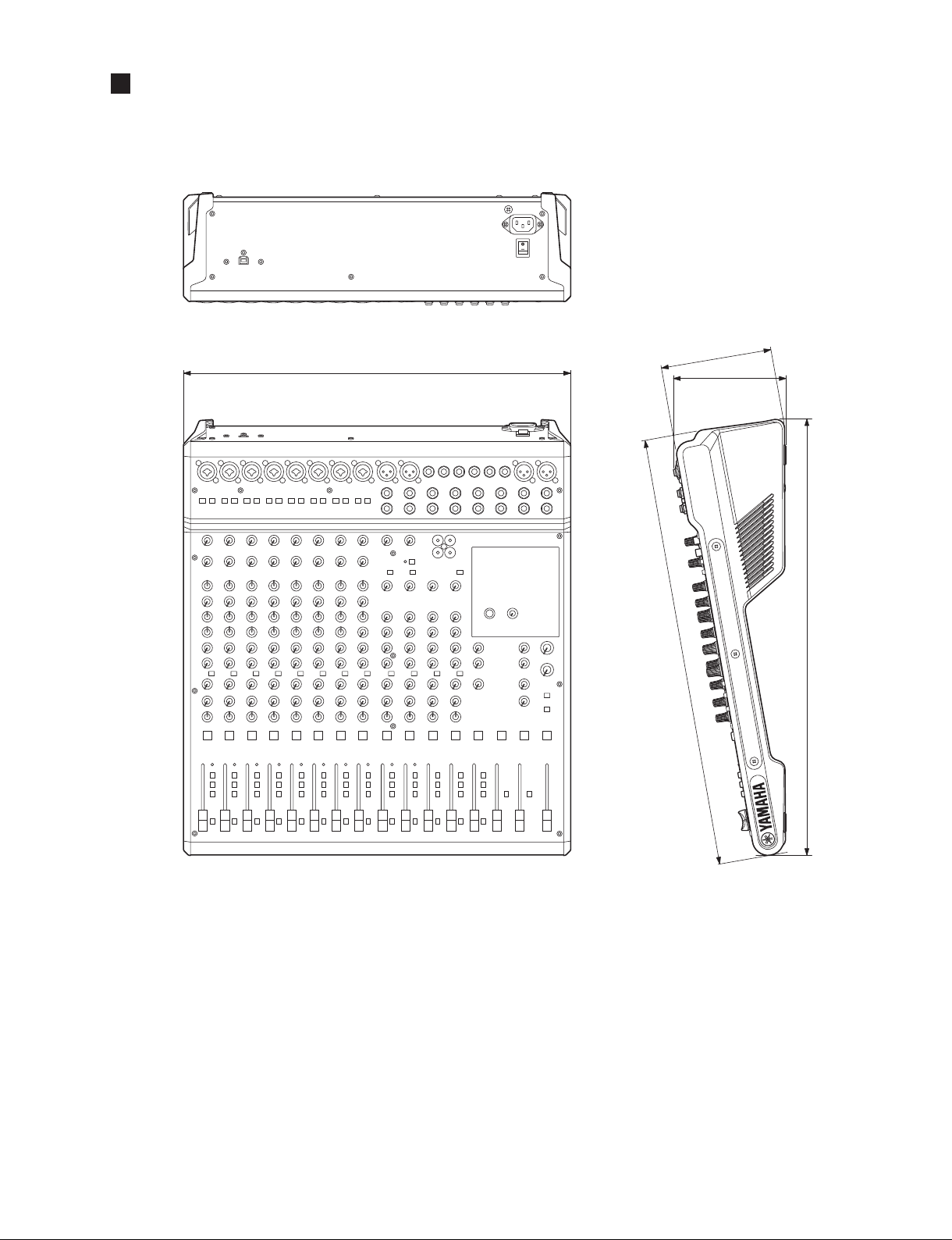
DIMENSIONS(寸法図)
Unit: mm
(単位)
MG16XU/MG16
444
128
130
500
493
※ This figure shows the MG16XU.
(この図は MG16XU です。)
7
MG16XU/MG16
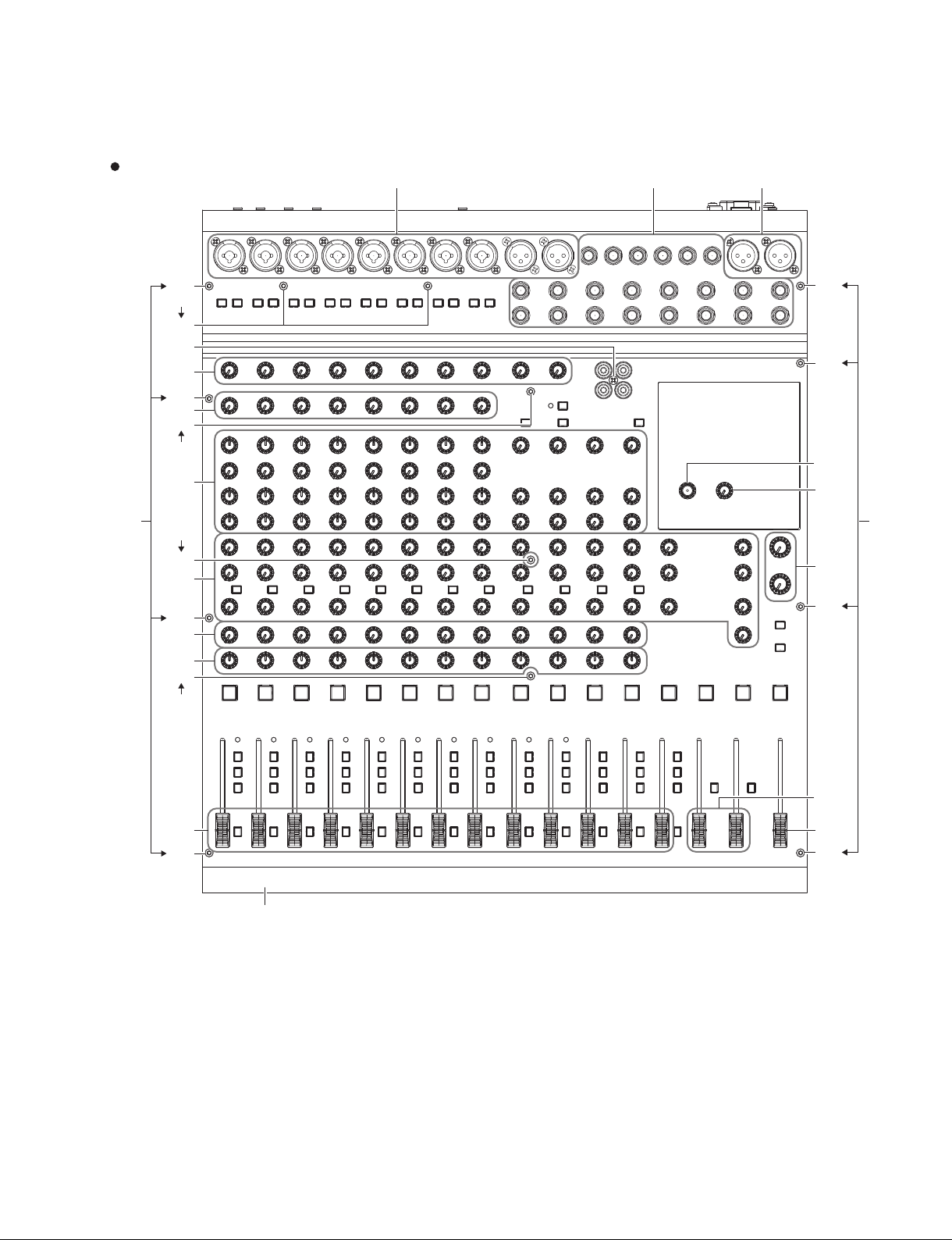
PANEL LAYOUT(パネルレイアウト)
Top panel (トップパネル)
:
@
;
=
.
B
2
>
=
8
4
/
0
)
Rear panel (リアパネル)
1 6 - *
2
※ This figure shows the MG16XU.
(この図は MG16XU です。)
8
MG16XU/MG16
Top panel Channel section
q [MIC/LINE] mono input jacks (channels 1-8)
w [MIC/LINE (L/MONO, R)] mono/stereo input
jacks (channels 9/10 and 11/12)
e [LINE (L, R)]
r [PAD] switch
t [HPF] (High Pass Filter) switch
y [GAIN] knobs
u [COMP] knobs
i [PHANTOM +48V] switch and indicator
o [LINE —/USB _] switch (MG16XU)
!0 Equalizer ([HIGH]/[MID]/[LOW])
!1 [AUX1-4] knobs (AUX1-3 : MG16XU) (AUX1-4 : MG16)
[PRE] switches
[AUX4/FX] knobs (MG16XU)
!2 [PAN] knobs
[PAN/BAL] knobs
[BAL] knobs
!3 [ON] switches
!4 [PEAK] indicators
!5 Bus assign switch
!6 [PFL] (Pre-fader Listen) switch
!7 Channel faders
stereo input jacks (channels 13/14 to 15/16)
Top panel Master section
!8 [SEND (AUX1-4)] jacks
!9 [GROUP OUT (1-4)] jacks
@0 [MONITOR OUT (L, R)] jacks
@1 [STEREO OUT (L, R)] jacks
@2 [PHONES] jack
[MONITOR] section
@3 [POWER] indicator
@4 Level meter
@5 [PFL] indicator
@6 [MONITOR LEVEL] knob
@7 [PHONES] knob
@8 [SOURCE]/[SOURCE SELECT]
(Monitor signal selection switch)
[SEND MASTER] section
@9 [AUX1-4] knobs
[GROUP] section
#0 [ON] switch
#1 [GROUP 1-2, 3-4] fader
#2 [ST] switch
[STEREO] section
#3 [ON] switch
#4 [STEREO] master fader
(Input: q to !7
(Output: !8 to #4
)
)
トップパネルチャンネルセクション(入力部
q [MIC/LINE] モノラル入力端子 ( チャンネル 1 〜 8)
w [MIC/LINE(L/MONO、R)] モノラル / ステレオ兼用
入力端子 ( チャンネル 9/10、11/12)
e [LINE(L、R)]
r [PAD] スイッチ
t [HPF]( ハイパスフィルター ) スイッチ
y [GAIN] つまみ
u [COMP] つまみ
i [PHANTOM+48V] スイッチ / インジケーター
o [LINE—/USB_]スイッチ ( M G16 XU)
!0 EQ( イコライザー [HIGH]/[MID]/[LOW])
!1 [AUX1-4]
[PRE] スイッチ
[AUX4/FX] つまみ (MG16XU)
!2 [PAN] つまみ
[PAN/BAL] つまみ
[BAL] つまみ
!3 [ON] スイッチ
!4 [PEAK] インジケーター
!5 バスアサインスイッチ
!6 [PFL]( プリフェーダーリッスン ) スイッチ
!7 チャンネルフェーダー
ステレオ入力端子 ( チャンネル13/14 〜 15/16)
ノブ (AUX1 〜 3:MG16XU)(AUX1 〜 4:MG16)
トップパネルマスターセクション(出力部
!8 [SEND(AUX1〜 4)] 端子
!9 [GROUPOUT(1〜 4)] 端子
@0 [MONITOROUT(L、R)] 端子
@1 [STEREOOUT(L、R)] 端子
@2 [PHONES] 端子
[MONITOR] セクション
@3 [POWER] インジケーター
@4 レベルメーター
@5 [PFL] インジケーター
@6 [MONITORLEVEL] つまみ
@7 [PHONES] つまみ
@8 [SOURCE]/[SOURCESELECT]
( モニター信号切り替えスイッチ )
[SENDMASTER] セクション
@9 [AUX1 〜 4] つまみ
[GROUP] セクション
#0 [ON] スイッチ
#1 [GROUP1-2、3-4] フェーダー
#2 [ST] スイッチ
[STEREO] セクション
#3 [ON] スイッチ
#4 [STEREO] マスターフェー ダー
q ~ !7)
!8 ~ #4)
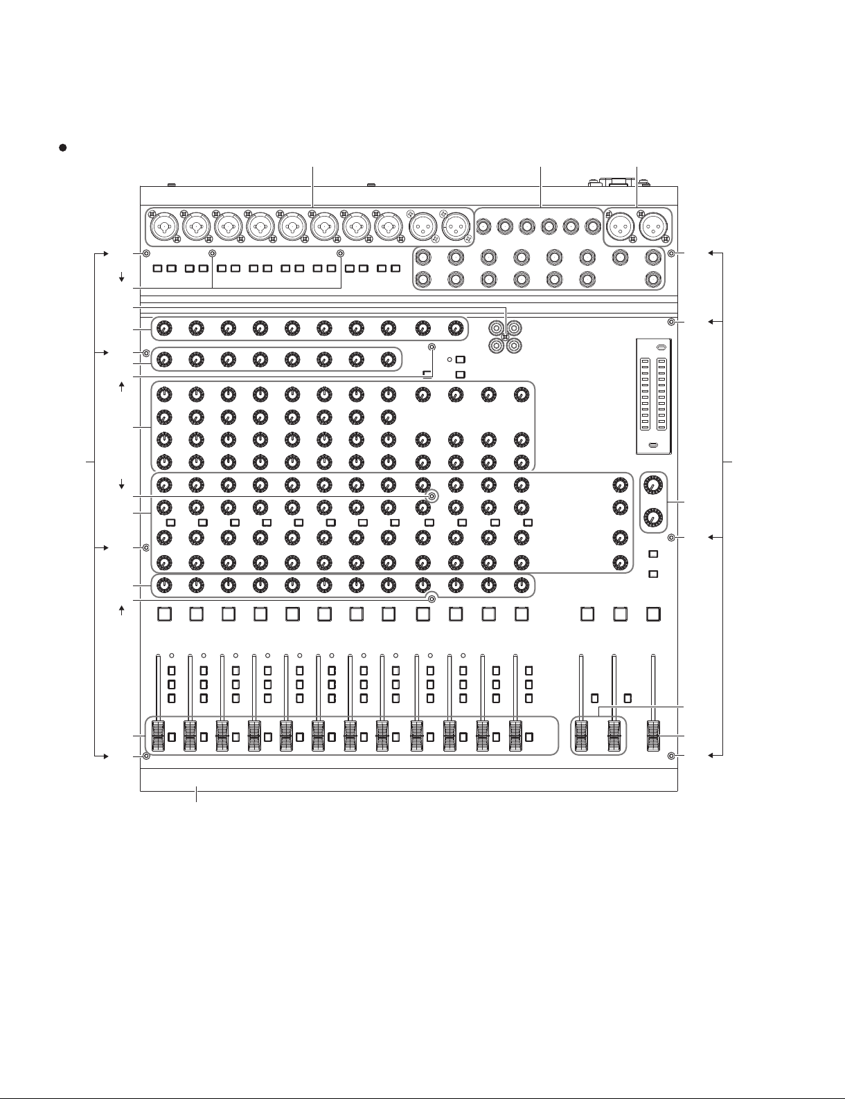
Top panel Internal effect section
(Output: q to !0) (MG16XU)
q Display
w Effect program list
e [PROGRAM] knob
r [PARAMETER] knob
t [AUX1-3] knob
y [ON] switch
u Bus assign switch
i [PFL] (Pre-fader Listen) switch
o [FX RTN] fader
!0 [FOOT SW] (Foot Switch) jack
Rear panel
#5 [ ]POWER switch
#6 [AC IN] jack
#7 [USB 2.0] terminal (MG16XU)
トップパネル内蔵エフェクトセクション
(出力部q ~ !0)(MG16XU)
q ディスプレ イ
w エフェクトプログラムリスト
e [PROGRAM] つまみ
r [PARAMETER] つまみ
t [AUX1 〜 3] つまみ
y [ON] スイッチ
u バスアサインスイッチ
i [PFL]( プリフェーダーリッスン ) スイッチ
o [FXRTN] フェーダー
!0 [FOOTSW]( フットスイッチ ) 端子
リアパネル
#5 [ ]電源スイッチ
#6 [ACIN] 端子
#7 [USB2.0] 端子 (MG16XU)
9
MG16XU/MG16
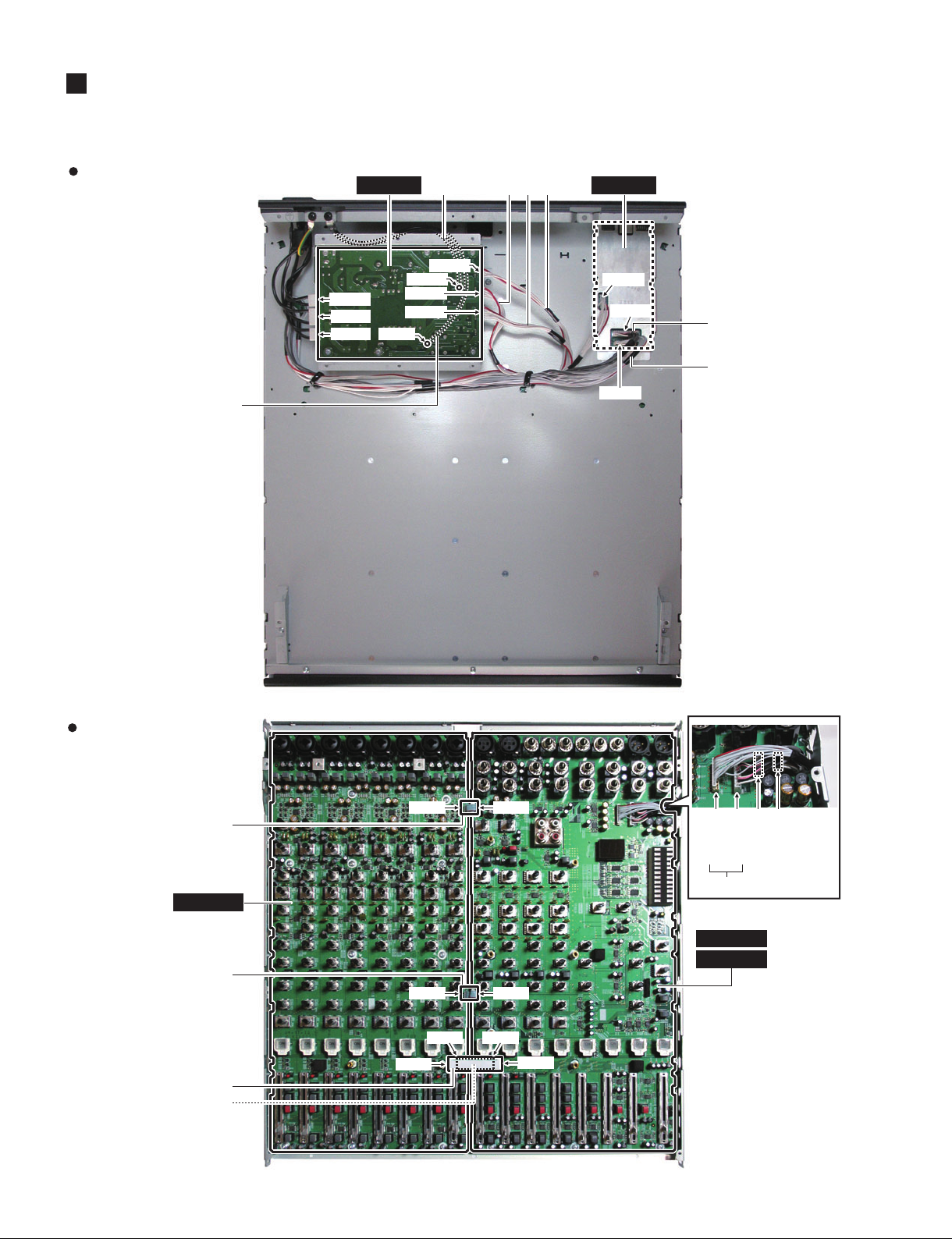
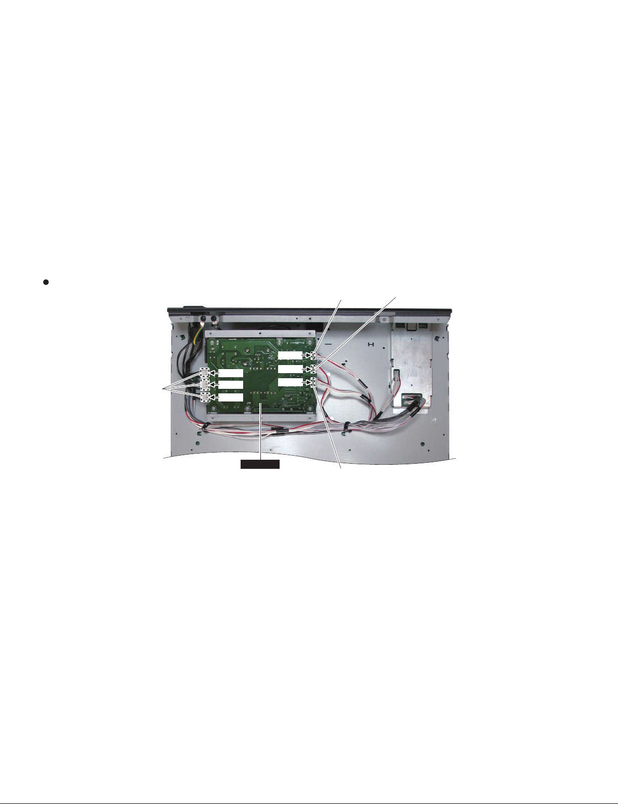
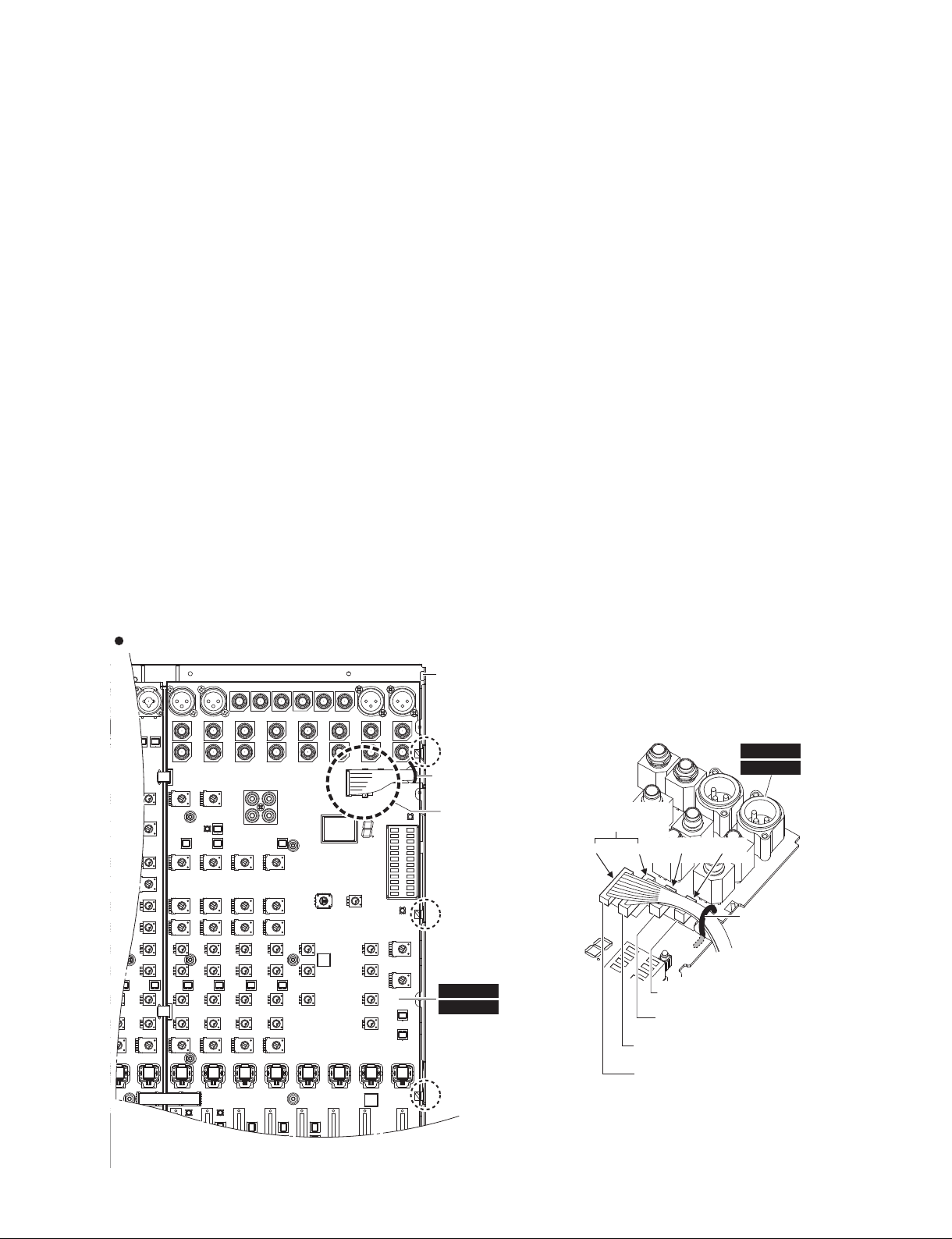
CIRCUIT BOARD LAYOUT & WIRING(ユニットレイアウト & 結線図)
Bottom view
(裏から見た図)
※ This photo shows the MG16XU.
(この写真は MG16XU です。)
B
CN103
CN101
CN102
PS20
CN106
CN107
CN109
CN104
>
CN105
DM12 assembly(DM12アッセイ)
;
.
=
DM12
CN501
CN503
CN502
(MG16XU)
@
:
Top view
(上から見た図)
※ This photo shows the MG16XU.
(この写真は MG16XU です。)
2
MONO16
8
CN101
CN102
CN104 CN202
CN103
CN101
CN203
CN201
CN602
CN802
CN801
:@.;
(MG16XU)
MAS16X
MAS16
CN601
(MG16XU)
(MG16)
10
MG16XU/MG16
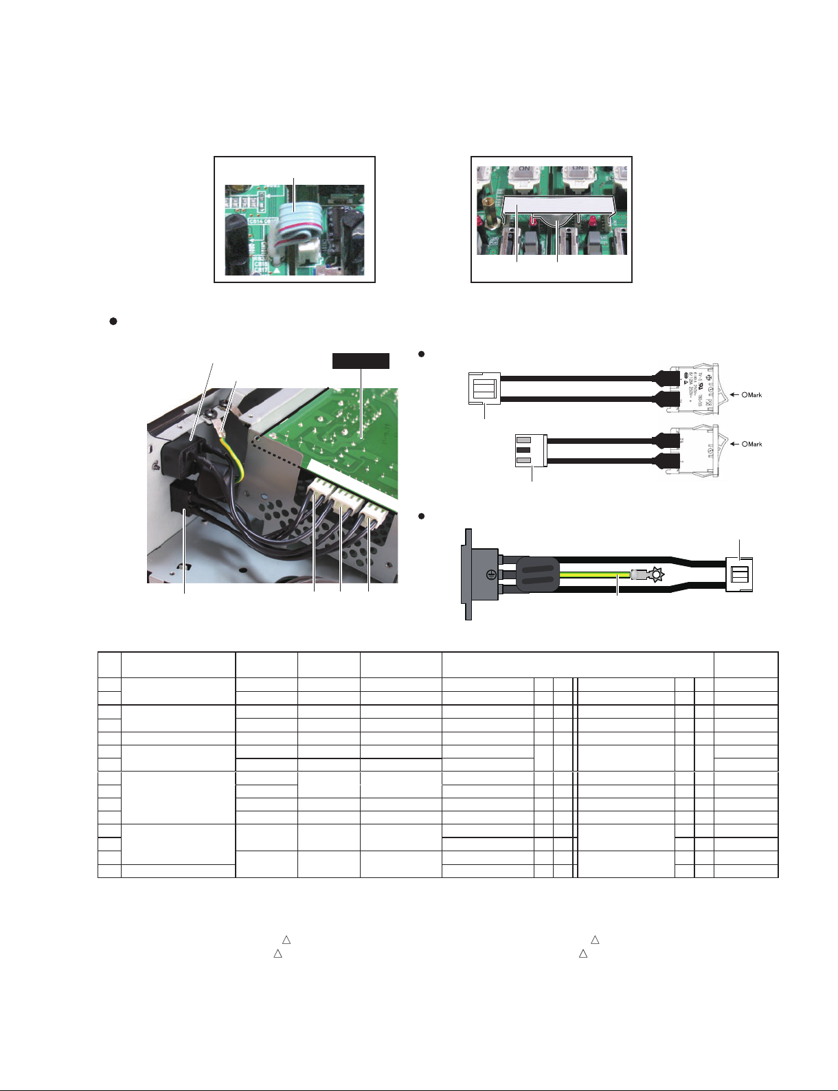
FFC CABLE(FFCケーブル)JUMPAR LEAD(ジャンパーリード)
2,8
AC inlet or PSW and PS20 circuit board wiring(AC インレットおよび電源スイッチと PS20 シートの結線 )
INLET20 connector assembly (AC inlet)
(INLET20束線(ACインレット))
PSW20 connector assembly
(POWER switch)
(PSW20束線(電源スイッチ))
No.
(ユニット名)
:
MAS16X (MG16XU)
@
.
MAS16X (MG16XU)/
MAS16 (MG16)
;
=
DM12 (MG16XU)
B
>
2
8
Unit Name
PS20
MONO16
PS20
Location
(ロケーション)
30 (ZJ66010) DM12-GH2
40 (ZJ98410) MAS16-DM12
50 (ZJ98400) MAS16-PS20
60 (ZJ98390) MAS16-PS20
450 (ZJ98420) DM12-PS20
--
--
--
-150 ZJ882200 FFC CABLE MONO16-CN104 *1 *3 *1 *3 9P L=40
160 ZJ882300 FFC CABLE MONO16-CN103 *1 *3 *1 *3 9P L=70
310 ZJ662300 PSW20
320 ZJ662200
PS20
CN103
CN101
Parts No.
(部品番号)
(ZJ66260)
(ZK13620)
(WU08270)
PSW20 connector assembly(PSW20束線)
CN102
INLET20 connector assembly(INLET20束線)
Connector Assembly
(束線名)
MAS16X/MAS16-CN602
MAS16X/MAS16-CN601
GND201
GND202
JUMPER LEAD
INLET20
3
1
1
3
L
N
Destination
MAS16X-CN801
MAS16X-CN802
DM12-CN501 *1 *4 PS20-CN109 *1 *4 5P L=260
PS20-CN106
PS20-CN107
MONO16-CN101 *2 *1 4P
MONO16-CN102 *2
PS20-CN103 *1 *3
PS20-CN102 *1 *3 *2
PS20-CN101 *1 *3
GND *5 *2 L=70
(配線先)
*1 *4 DM12-CN502 *1 *4 15P L=570
*1 *3 DM12-CN503 *1 *3 11P L=550
*1 *4 PS20-CN104 *1 *4 6P L=530
*1 *4 PS20-CN105 *1 *4 4P L=530
*2
GND
MAS16X/MAS16-CN101
MAS16X/MAS16-CN203
MAS16X/MAS16-CN202
MAS16X/MAS16-CN201
POWER switch
(電源スイッチ)
AC inlet (ACインレット)
*5
*1 4P
*2 3P L=110
*2 4P L=135
1
4
Remarks
(備考)
L=230
L=180
3P L=130
* The parts with “( )” in “Part No.” are not available as spare parts.
*1: Installation
*2: Manual soldering
*3: Edge mark is adjusted to Pin 1 mark (
*4: Red wire is adjusted to Pin 1 mark ( mark).
*5: Screw
mark).
*部品番号が()で囲まれている部品は、サービス部品として準備されていません。
*1: 差込み
*2: 手半田
*3: エッジマークが 1 ピン側(
*4: 赤色線材が 1 ピン側(
*5: ネジ締め
)
)
11
&
MG16XU/MG16
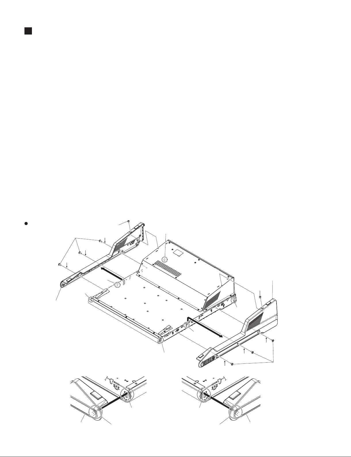
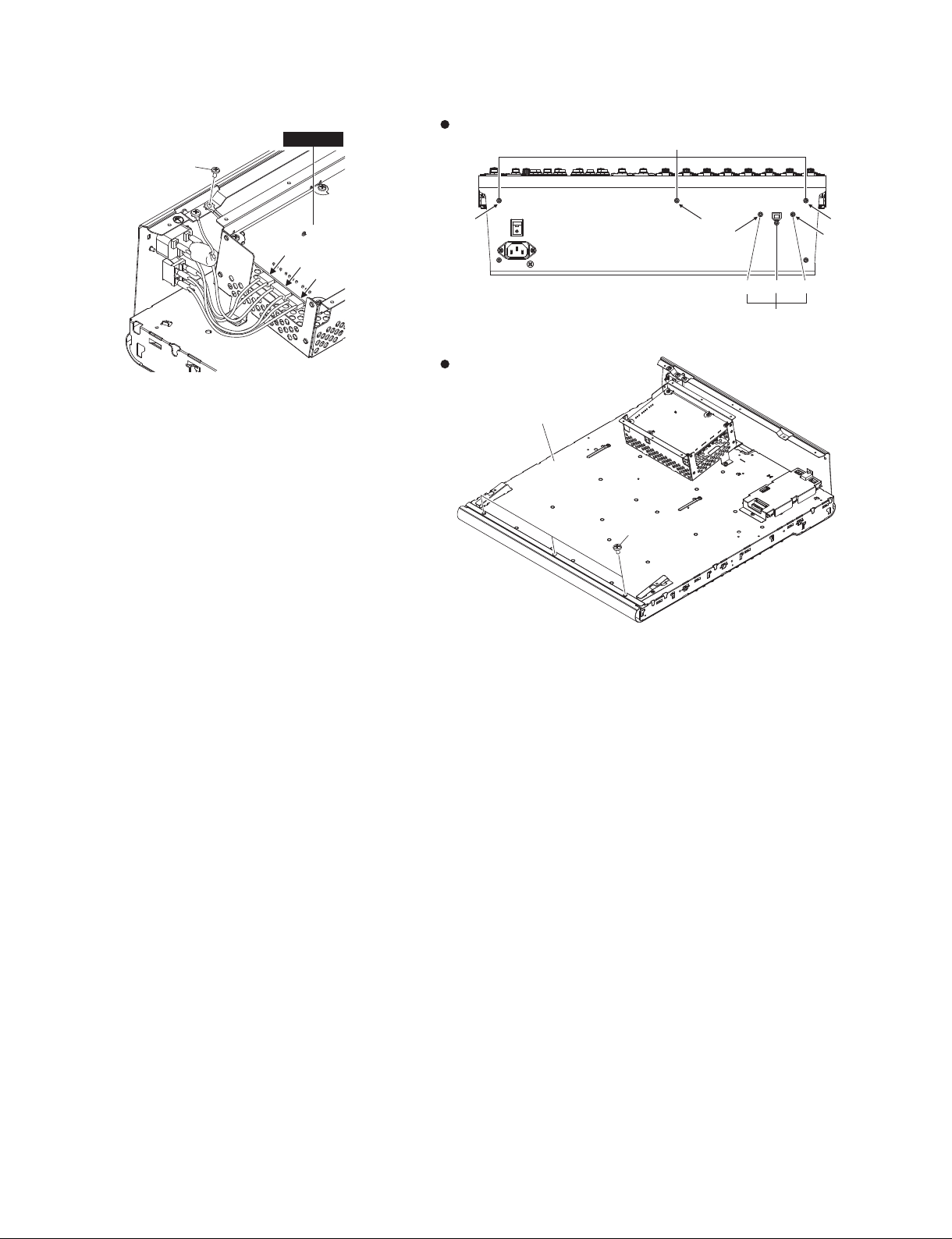
DISASSEMBLY PROCEDURE(分解手順)
1. SIDE PAD (L, R) 16 ASSEMBLY (Time required: About 2 minutes each)
1-1. SIDE PAD L 16 ASSEMBLY
1-1-1. Reverse the unit and remove the three (3) screws
marked [620A] and the screw marked [630A]. (Fig.1)
* When installing the Side pad L 16 assembly, tighten
the screws marked [620A] in the order of a, b and c.
(Fig. 1)
1-1-2. Slide the Side pad L 16 assembly in the directions of the
arrows in Fig. 1 from the hooks (3 places). (Fig. 1)
* When installing the Side pad L 16 assembly, insert the
hooks into the holes, and fasten by lowering. (Fig. 2)
1-2. SIDE PAD R 16 ASSEMBLY
1-2-1. Reverse the unit and remove the three (3) screws
marked [620B] and the screw marked [630B]. (Fig.1)
* When installing the Side pad R 16 assembly, tighten
the screws marked [620B] in the order of a, b and c.
(Fig. 1)
1-2-2. Slide the side pad R 16 assembly in the directions of the
arrows in Fig. 1 from the hooks (3 places). (Fig. 1)
* When installing the Side pad R 16 assembly, insert the
hooks into the holes, and fasten by lowering. (Fig. 2)
Bottom view (下から見た図)
[620B]
[630B]
(
Hole
(穴)
1. サイドパッド(L,R)16 アッセイ
(所要時間:各約 2 分)
1-1. サイドパッド L16 アッセイ
1-1-1. 本体を裏返し、[620A]のネジ 3 本と [630A]のネジ
1 本を外します。(図1)
※ サイドパッド L16 アッセイを取り付けるときは、[620A]
のネジをa、b、cの順番でネジ締めしてください。(図1)
1-1-2. サイドパッド L16 アッセイを 3 ヶ所にあるフック
から、図1の矢印の方向にずらして外します。(図1)
※ サイドパッド L16 アッセイを取り付けるときは、穴にフック
を挿入し、下にずらして引っ掛けてください。(図2)
1-2. サイドパッド R16 アッセイ
1-2-1. 本体を裏返し、[620B]のネジ 3 本と [630B]のネジ
1 本を外します。(図1)
※ サイドパッド R16 アッセイを取り付けるときは、[620B]
のネジをa、b、cの順番でネジ締めしてください。(図1)
1-2-2. サイドパッド R16 アッセイを 3 ヶ所にあるフック
から、図1の矢印の方向にずらして外します。(図1)
※ サイドパッド R16 アッセイを取り付けるときは、 穴にフック
を挿入し、下にずらして引っ掛けてください。(図2)
&
SIDE PAD R 16 ASSEMBLY
(サイドパッドR16 アッセイ)
Hole
(穴)
'
Hole
(穴)
Hole x3
(穴3ヶ所)
Hole
(穴)
Fig. 1
(図1)
Hole
(穴)
Hole x3
(穴3ヶ所)
Hole
(穴)
SIDE PAD L 16 ASSEMBLY
(サイドパッドL16アッセイ)
[630A]
(
'
[620A]
12
SIDE PAD R 16 ASSEMBLY
(サイドパッドR16アッセイ)
Hook x3
(フック3ヶ所)
Fig. 2
(図2)
Hook x3
(フック3ヶ所)
SIDE PAD L 16 ASSEMBLY
(サイドパッドL16アッセイ)
MG16XU/MG16
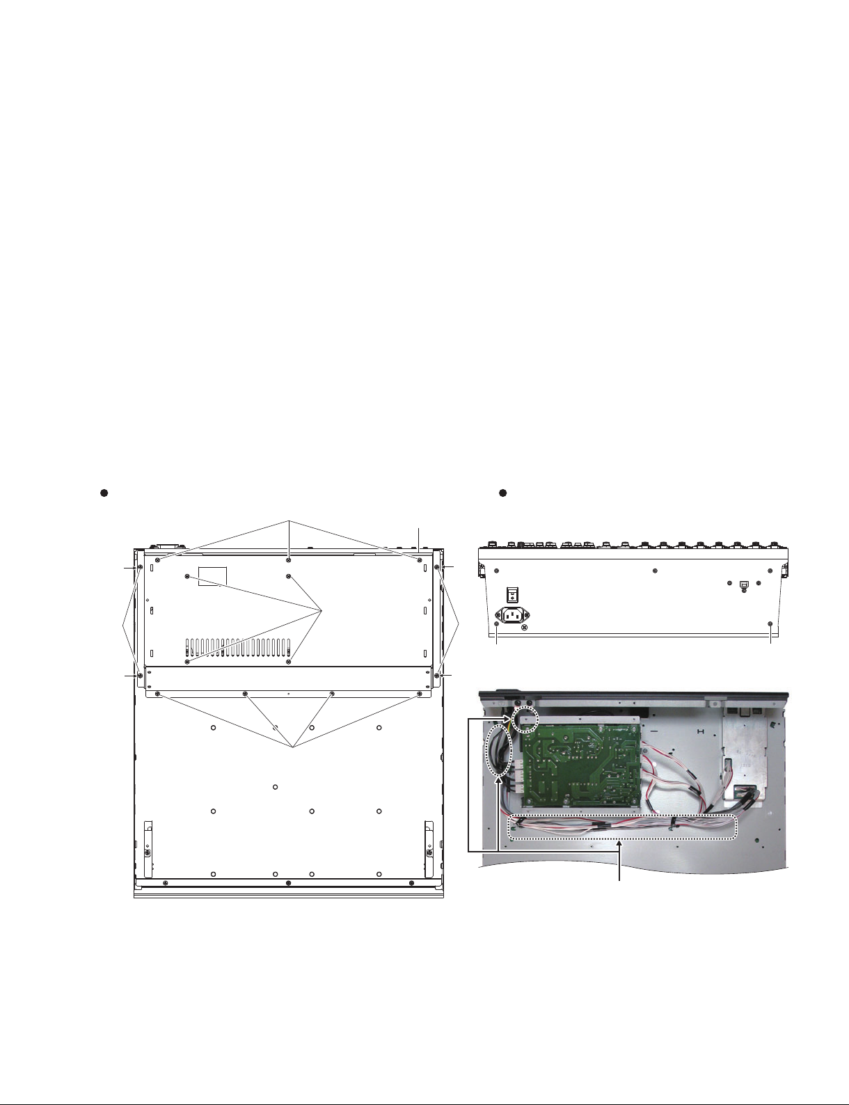
2. BOTTOM COVER 16X
(Time required: About 10 minutes)
2-1. Remove the Side pad (L, R) 16 assembly.
(See procedure 1)
2-2. Remove the two (2) screws marked [520], eight (8)
screws marked [530], three (3) screws marked [540]
and four (4) screws marked [550]. The Bottom cover
16X can then be removed. (Fig. 3-1, Fig. 3-2)
* When installing the Bottom cover 16X, first tighten
the screw [520], and then tighten the screws [530],
[540], [550] in the sequence of q- r as shown in the
figure. (Fig. 3-1, Fig. 3-2)
* Tighten the screws marked [530] in the order of a,
and then tighten the remaining screws. (Fig. 3-1)
b
* When installing the Bottom cover 16X, be careful not
to damage the cabling. (Fig. 3-3)
2. ボトムカバー 16X(所要時間:約 10 分)
2-1. サイドパッド(L,R)16 アッセイを外します。
(1項参照)
2-2. [520] のネジ 2 本、[530] のネジ 8 本、[540] のネジ
3 本、[550] のネジ 4 本を外し、ボトムカバー 16X
を外します。(図3-1、図3-2)
※ ボトムカバー 16X を取り付けるときは、[520]のネジを
先に締めてから、[530]、[540]、[550]のネジを図中の
q〜r
※ [530] のネジはa、b、その他の順番でネジ締めをして
ください。(図3-1)
※ ボトムカバー 16Xを取り付けるときは、束線を傷つけ
ないように注意してください。(図3-3)
の順に締めてください。( 図3-1、図3-2)
Bottom view (下から見た図) Rear view (背面から見た図)
'
[540]
BOTTOM COVER 16X
(ボトムカバー16X)
[530]
&
&
2
[550]
'
[530]
'
66
[530]
[520]
1
Fig. 3-2
(図3-2)
[520]
1
6
Don't pinch the wiring assembly of this place by a bottom cover.
(この場所 の束線をボトムカバーで挟まないようにしてください。)
Fig. 3-1
(図3-1)
※ This figure shows the MG16XU.
(この図は、MG16XU です。)
Fig. 3-3
(図3-3)
13
MG16XU/MG16
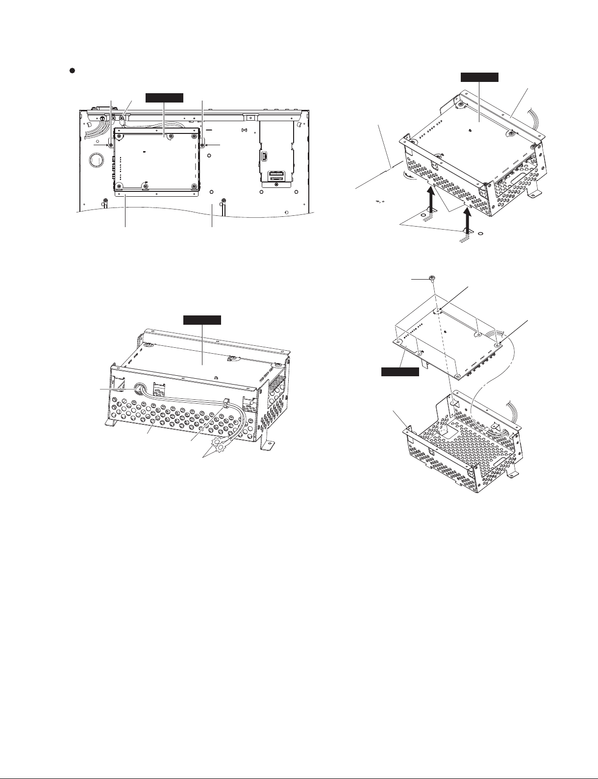
3. PS20 CIRCUIT BOARD (Time required: About 15 minutes)
3-1. Remove the Side pad (L, R) 16 assembly.
(See procedure 1)
3-2. Remove the Bottom cover 16X. (See procedure 2)
3-3. MG16XU:
Remove the six (6) connectors from the PS20 circuit
board. (Fig.4)
MG16:
Remove the fi ve (5) connectors from the PS20 circuit
board. (Fig.4)
* Refer to the CIRCUIT BOARD LAYOUT & WIRING (10-
11 page) for attachment the connector assemblies.
Bottom view (下から見た図)
※ This figure shows the MG16XU.
(この図は、MG16XU です。)
CN103
Connector assembly
(コネクター)
CN101
CN102
Connector assembly
CN105
CN109
CN104
3. PS20 シート(所要時間:約 15 分)
3-1. サイドパッド(L,R)16 アッセイを外します。
(1項参照)
3-2. ボトムカバー 16X を外します。(2項参照)
3-3. MG16XU:
PS20 シートからコネクター 6 ヶ所を外します。
(図4)
MG16:
PS20 シートからコネクター 5 ヶ所を外します。
(図4)
※ コネクターの取り付けは、ユニットレイアウト & 結線図
(10 〜 11 ページ)を参照してください。
(コネクター)
Connector assembly (MG16XU only)
(コネクター(MG16XUのみ))
PS20
3-4. Remove the two (2) screws marked [390] and the screw
marked [400]. (Fig.5-1)
* Tighten the screws marked [390] in the order of a
and b. (Fig. 5-1)
3-5. Slide the Shield PS 16 in the direction of the arrows in
Fig. 5-2, and remove the hook from the Shield mix 16X
assembly. The PS20 circuit board can then be removed
together with the Shield PS 16. (Fig. 5-2)
* During assembly, check that the hooks have been
inserted (2 locations). (Fig. 5-2)
3-6. Remove the ground wire from the mini clamp marked
[380] and remove the six (6) screws marked [370]. The
PS20 circuit board and the Shield PS 16 can then be
separated. (Fig. 6-1, Fig. 6-2)
* When installing the PS20 circuit board, Pass the
ground wire of the PS20 circuit board through the
hole of the Shield PS 16 before tightening the screw
on [370]. (Fig. 6-2)
* Tighten the screws marked [370] in the order of a,
and then tighten the remaining screws. (Fig. 6-2)
b
Fig. 4
Connector assembly
(コネクター)
(図4)
3-4. [390] のネジ 2 本と [400] のネジ 1 本を外します。
(図5-1)
※ [390] のネジは、a、bの順にネジ締めをしてください。
(図5-1)
3-5. シールド PS16 を図5-2 の矢印の方向にスライド
させて、フックをシールドMIX16XAss'yから外し、
シールド PS16 と共に PS20 シートを外します。
(図5-2)
※ 組立時は、フックが差し込まれていることを確認して
ください(2 ヶ所)。(図5-2)
3-6. [380] のミニクランプからグランド線を外し、[370]
のネジ 6 本を外して PS20 シートとシールド PS16
を分けます。(図6-1、図6-2)
※ PS20 シートを取り付ける時には、[370] のネジを締める
前に PS20 シートのグランド線をシールド PS16 の穴に
通します。(図6-2)
※ [370] のネジは、a、b、その他の順でネジ締めをして
ください。(図6-2)
14
MG16XU/MG16
Bottom view (下から見た図)
[400]
&
Shield PS 16
(シールドP S 16)
PS20
Shield mix 16X assembly
(シールドMIX16XAss'y)
Fig. 5-1
(図5-1)
[390][390]
PS20
PS20
Shield mix 16X assembly
(シールドMIX16XAss'y)
'
Hook
(フック)
Fig. 5-2
(図5-2)
&
※ This figure shows the MG16XU.
(この図は、MG16XU です。)
Hole
(穴)
[370]
Shield PS 16
(シールドP S 16)
'
Hole
(穴)
Shield PS 16
(シールドP S 16)
GND wire(GN D線)
[380]
Fig. 6-1
(図6-1)
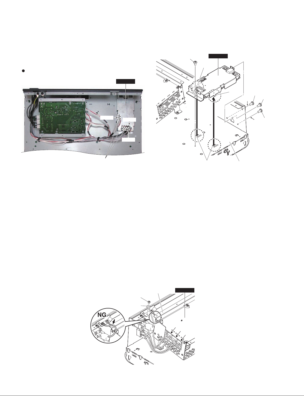
4. DM12 ASSEMBLY (MG16XU only) (Time required: About 13 minutes)
4-1. Remove the Side pad (L, R) 16 assembly.
(See procedure 1)
4-2. Remove the Bottom cover 16X. (See procedure 2)
4-3. Remove the three (3) connectors from the DM12
assembly. (Fig.7-1)
* Refer to the CIRCUIT BOARD LAYOUT & WIRING (10-
11 page) for attachment the connector assemblies.
4-4. Remove the two (2) screws marked [420], screw
marked [430] and screw marked [440]. (Fig.7-2)
* Tighten the screws marked [420] in the order of a
and b. (Fig. 7-2)
4-5. Slide the DM12 assembly in the direction of the arrows
in Fig. 7-2, and remove the hook from the Shield Mix
16X assembly. (Fig.7-2)
* During assembly, check that the hooks have been
inserted (2 locations). (Fig. 7-2)
PS20
Shield PS 16
(シールドP S 16)
Fig. 6-2
(図6-2)
4. DM12 アッセイ(MG16XU のみ) (所要時間:約 13 分)
4-1. サイドパッド(L,R)16 アッセイを外します。
(1項参照)
4-2. ボトムカバー 16X を外します。(2項参照)
4-3. DM12 アッセイからコネクター 3 ヶ所を外します。
(図7-1)
※ コネクターの取り付けは、ユニットレイアウト & 結線図
(10 〜 11 ページ)を参照してください。
4-4. [420] のネジ 2 本、[430] のネジ 1 本と [440] のネジ
1 本を外します。(図7-2)
※ [420] のネジは、a、bの順にネジ締めをしてください。
(図7-2)
4-5. DM12 アッセイを図7-2 の矢印の方向にスライド
させて、フックをシールド MIX16XAss'y から外し
ます。(図7-2)
※ 組み立てるときには、フックが差し込まれていることを
確認してください(2 ヶ所)。(図 7-2)
15
MG16XU/MG16
Bottom view (下から見た図)
Fig. 7-1
(図7-1)
DM12 assembly
(DM12アッセイ)
CN501
Connector assembly
(コネクター)
DM12
CN503
CN502
[440]
Hook
(フック)
Hole
(穴)
Fig. 7-2
DM12
(図7-2)
DM12 assembly
(DM12アッセイ)
Hook
(フック)
Shield mix 16X assembly
(シールドMIX16XAss'y)
[420]
'
&
[430]
[420]
5 . PSW20 (POWER SWITCH) and INLET20
(AC INLET) CONNECTOR ASSEMBLY
(Time required: About 13 minutes each)
5-1. Remove the Side pad (L, R) 16 assembly.
(See procedure 1)
5-2. Remove the Bottom cover 16X. (See procedure 2)
5-3. Disconnect the connector assemblies from the
connector CN101 (4P), CN102 (3P) and CN103 (3P) of
the PS20 circuit board, and remove the screw marked
[340]. (Fig.8)
* Refer to the CIRCUIT BOARD LAYOUT & WIRING (11
page) for attachment the connector assemblies.
GND wire
(GN D線)
(シールドP S 16)
[340]
5. PSW20 束 線(電源スイッチ)、INLET20 束線(AC インレット)
(所要時間:各約 13 分)
5-1. サイドパッド(L,R)16 アッセイを外します。
(1項参照)
5-2. ボトムカバー 16X を外します。(2項参照)
5-3. PS20 シートの CN101(4P)、CN102(3P)と CN103(3P)
に接続されている束線を外し、[340] のネジ 1 本を外
します。(図8)
※ コネクターの取り付けは、ユニットレイアウト & 結線図
(11 ページ)を参照してください。
Shield PS 16
CN103
CN101
PS20
CN102
16
Fig. 8
(図8)
MG16XU/MG16
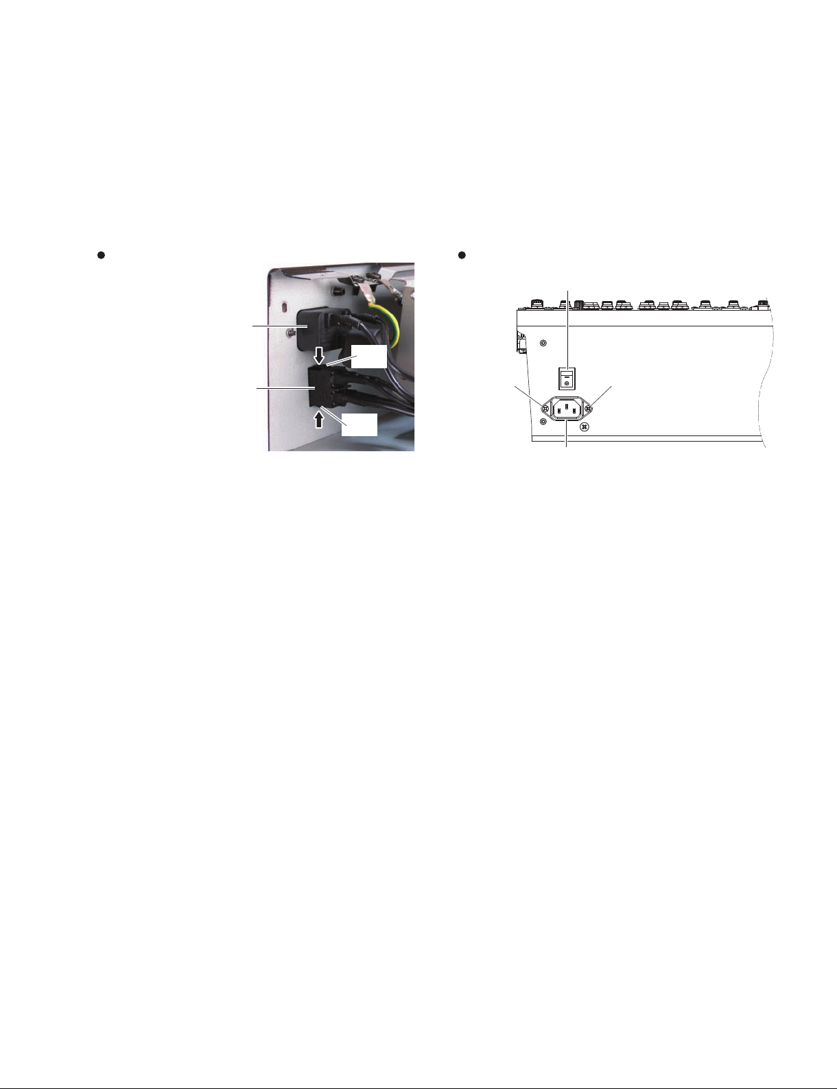
5-4. PSW20 connector assembly (POWER SWITCH)
5-4-1. Remove the power switch of the PSW20 connector
assembly by pressing its claws. (Fig. 9)
* When installing the PSW20 connector assembly,
install the power switch in the direction shown in
Fig. 10. (Fig. 10)
Side view (側面から見た図)
INLET20 connector assembly
(INLET2 0束線(ACインレット))
(AC INLET )
PSW20 connector assembly
(POWER SWITCH)
(PSW20束線(電源スイッチ))
Fig. 9
Claw
(ツメ)
Claw
(ツメ)
(図9)
5-5. INLET20 connector assembly (AC INLET)
5-5-1. Remove the two (2) screws marked [330] . The
INLET20 connector assembly can then be removed.
(Fig. 10)
* Install the INLET20 connector assembly (AC inlet) in
the direction shown in Fig. 10. (Fig. 10)
* GND wire of INLET20 connector assembly is kept
from coming over the screw hole of Shield PS16.
(Fig. 8)
5-4. PSW20 束線(電源スイッチ)
5-4-1. PSW20 束線の電源スイッチのツメを押して外し
ます。(図9)
※ PSW20 束線(電源スイッチ)を取り付ける時には、図10
の方向で取り付けてください。(図10)
Rear view (背面から見た図)
PSW20 connector assembly (POWER SWITCH)
(PSW20束線(電源スイッチ))
[330][330]
INLET20 connector assembly (AC INLET)
(INLET2 0束線(ACインレット))
Fig. 10
(図10)
5-5. INLET20 束線(AC インレット)
5-5-1. [330] のネジ 2 本を外し、INLET20 束線(AC イン
レット)を外します。(図10)
※ INLET20 束線(AC インレット)を取り付ける時には、
図10の方向で取り付けてください。(図10)
※ INLET20 束線の GND 線がシールド PS16 のネジ穴の上
に来ないようにしてください。(図8)
6. TOP COVER (Time required: About 42 minutes)
6-1. Remove the Side pad (L, R) 16 assembly.
(See procedure 1)
6-2. Remove the Bottom cover 16X. (See procedure 2)
6-3. Disconnect the connector assemblies from the
connector CN101 (4P), CN102 (3P) and CN103 (3P) of
the PS20 circuit board, and remove the screw marked
[400]. (Fig.11)
* Refer to the CIRCUIT BOARD LAYOUT & WIRING (11
page) for attachment the connector assemblies.
6-4. MG16XU :
Remove the three (3) screws marked [260], two (2)
screws marked [420], the screw marked [430] and three
(3) screws marked [560]. (Fig. 12-1, Fig. 12-2)
MG16 :
Remove the three (3) screws marked [260] and three (3)
screws marked [560]. (Fig. 12-1, Fig. 12-2)
* During assembly, first tighten the screws marked [260]
in the order of
[420] (MG16XU only) in the order of
-
, and then tighten screws marked
a
c
and e . (Fig. 12-1)
d
6. トップカバー(所要時間:約 42 分)
6-1. サイドパッド(L,R)16 アッセイを外します。
(1項参照)
6-2. ボトムカバー 16X を外します。(2項参照)
6-3. PS20 シートの CN101(4P)、CN102(3P)と CN103(3P)
に接続されている束線を外し、[400] のネジ 1 本
を外します。(図11)
※ コネクターの取り付けは、ユニットレイアウト & 結線図
(11 ページ)を参照してください。
6-4. MG16XU:
[260] のネジ 3 本、[420] のネジ 2 本、[430] のネジ
1本と [560] のネジ 3 本を外します。
(図12-1、図12-2)
MG16:
[260] のネジ 3 本と [560] のネジ 3 本を外します。
(図12-1、図12-2)
※ 組み立てるときには、初めに [260] のネジをa〜cの
順でネジ締めをしてから [420] の ネジ (MG16XU のみ )
を、d、eの順にのネジを締めてください。(図12-1)
17
MG16XU/MG16
PS20
[400]
CN103
CN101
CN102
Fig. 11
(図11)
6-5. MG16XU :
Remove the twenty-three (23) KNOB VR SMALL
WHITE/BLACKs marked [640], eight (8) KNOB VR
SMALL YELLOW/BLACKs marked [650], forty-
four (44) KNOB VR SMALL GREEN/BLACKs
marked [660], forty- three (43) KNOB VR SMALL
BLUE/BLACKs marked [670], twelve (12) KNOB VR
SMALL RED/BLACKs marked [680], two (2) KNOB
LEVEL WHITE/BLACKs marked [690], thirteen (13)
KNOB FADER BLACK/L-GRAYs marked [700], two
(2) KNOB FADER RED/D-GRAYs marked [710], the
KNOB FADER WHITE/RED marked [720] and the
ENCODER MG3 BLACK marked [730]. (Fig. 13-1)
MG16 :
Remove the ten (10) KNOB VR SMALL WHITE/
BLACKs marked [640], eight (8) KNOB VR SMALL
YELLOW/BLACKs marked [650], forty- four (44)
KNOB VR SMALL GREEN/BLACKs marked [660],
fi fty-two (52) KNOB VR SMALL BLUE/BLACKs
marked [670], twelve (12) KNOB VR SMALL RED/
BLACKs marked [680], two (2) KNOB LEVEL
WHITE/BLACKs marked [690], twelve (12) KNOB
FADER BLACK/L-GRAYs marked [700], two (2)
KNOB FADER RED/D-GRAYs marked [710] and the
KNOB FADER WHITE/RED marked [720]. (Fig. 13-2)
6-6. MG16XU :
Remove the thirteen (13) screws marked [230], twenty-
fi ve (25) screws marked [240] and twenty-two (22)
each hexagonal nuts and washers marked [A]. The Top
cover can then be removed. (Fig. 13-1)
MG16 :
Remove the thirteen (13) screws marked [230], twenty-
fi ve (25) screws marked [240] and twenty-one (21) each
hexagonal nuts and washers marked [A]. The Top cover
can then be removed. (Fig. 13-2)
* During assembly, first tighten the screws marked
[230] in the order of
remaining screws, and then tighten screws marked
[240]. (Fig. 13-1 (MG16XU), Fig. 13-2 (MG16))
-
and then tighten the
a
e
Rear view (背面から見た図)
[260]
'
※ This figure shows the MG16XU.
(この図は、MG16XU です。)
Fig. 12-1
(図12-1)
&
*
MG16XU only
(MG16XUのみ)
Bottom view (底面から見た図)
Shield mix 16X assembly
(シールドMIX16XAss'y)
[560]
※ This figure shows the MG16XU.
(この図は、MG16XU です。)
Fig. 12-2
(図12-2)
6-5. MG16XU:
[640] のノブ VR小23個、[650] のノブ VR小8個、
[660] のノブ VR小44個、[670] のノブ VR小43個、
[680] のノブ VR小12個、[690] のノブ LEVEL2個、
[700] のノブ FADER13 個、[710] の ノブ FADER
2個、[720] のノブ FADER1個と [730] のエンコーダ
MG31個を外します。(図13-1)
MG16:
[640] のノブ VR小10個、[650] のノブ VR小8個、
[660] のノブ VR小44個、[670] のノブ VR小52 個、
[680] のノブ VR小12個、[690] のノブ LEVEL2個、
[700] のノブ FADER12 個、[710] の ノブ FADER
2個と [720] のノブ FADER1個を外します。
(図13-2)
6-6. MG16XU:
[230] のネジ 13 本、[240] のネジ 25 本と [A] の六角
ナットとワッシャー 22個ずつを外し、トップカバー
を外します。(図13-1)
MG16:
[230] のネジ 13 本、[240] のネジ 25 本と [A] の六角
ナットとワッシャー 21個ずつを外し、トップカバー
を外します。(図13-2)
※ 組み立てるときには、初めに [230] のネジをa〜e、
その他の順でネジ締めをしてから [240] のネジを締めて
ください。(図13-1(MG16XU)、図 13-2(MG16))
(
)
[430][420] [420]
18
MG16XU/MG16
Top view (上から見た図)
Model : MG16XU
[230]
*
[230]
[240]
[640]
[230]
[650]
[230]
'
[660]
)
&
[230]
[670]
[230]
[640]
[680]
[230]
(
[A][240]
[240]
[230]
[230]
[730]
[640]
)
[690]
[230]
[710]
[700] [720]
[230]
Top co ve r(トップカバー)
[640]: KNOB VR SMALL WHITE/BLACK(ノブVR小)
[650]: KNOB VR SMALL YELLOW/BLACK(ノブVR小)
[660]: KNOB VR SMALL GREEN/BLACK(ノブVR小)
[670]: KNOB VR SMALL BLUE/BLACK(ノブVR小)
[680]: KNOB VR SMALL RED/BLACK(ノブVR小)
Fig. 13-1
[690]: KNOB LEVEL WHITE/BLACK(ノブL EV E L)
[700]: KNOB FADER BLACK/L-GRAY(ノブFA D ER )
[710]: KNOB FADER RED/D-GRAY(ノブFA D ER )
[720]: KNOB FADER WHITE/RED(ノブFA D ER )
[730]: ENCODER MG3 BLACK(エンコーダMG3)
(図13-1)
[230]
19
MG16XU/MG16
Top view (上から見た図)
Model : MG16
[230]
*
[230]
[240]
[640]
[230]
[650]
[230]
'
[660]
)
&
[230]
[670]
[230]
[A][240]
[240]
[230]
[230]
)
[690]
[230]
[680]
[230]
(
[710]
[700] [720]
[230]
Top co ve r(トップカバー)
[640]: KNOB VR SMALL WHITE/BLACK(ノブVR小)
[650]: KNOB VR SMALL YELLOW/BLACK(ノブVR小)
[660]: KNOB VR SMALL GREEN/BLACK(ノブVR小)
[670]: KNOB VR SMALL BLUE/BLACK(ノブVR小)
[680]: KNOB VR SMALL RED/BLACK(ノブVR小)
Fig. 13-2
[690]: KNOB LEVEL WHITE/BLACK(ノブL EV E L)
[700]: KNOB FADER BLACK/L-GRAY(ノブFA D ER )
[710]: KNOB FADER RED/D-GRAY(ノブFA D ER )
[720]: KNOB FADER WHITE/RED(ノブFA D ER )
(図13-2)
[230]
20

MG16XU/MG16
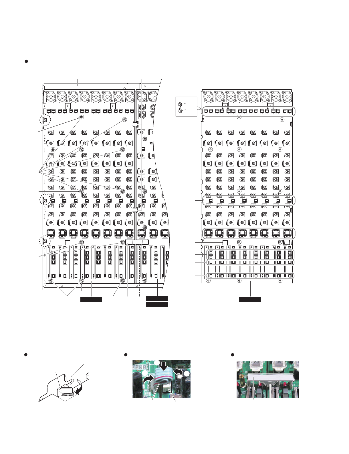
Disassembly of MONO16 CIRCUIT
BOARD, MAS16X (MG16XU) /MAS16
(MG16) CIRCUIT BOARD
* Before disassembly, remove the Top cover in
advance. (See procedure 6 on page 17)
7. MONO16 CIRCUIT BOARD (Time required: About 23 minutes)
7-1. Turn the three (3) claws fi xing the MONO16 circuit
board to be aligned parallel to each other.
(Fig. 14-1, Fig. 14-3)
* When installing the circuit board, twist the claws
within the white frame to fix the MONO16 circuit
board. (Fig. 14-3)
Be sure that the MONO16 circuit board is fixed
securely without rattling.
7-2. Disconnect the FFC cable marked [150] and [160],
the two (2) jumper leads from the connector of the
MAS16X circuit board (MG16XU) or MAS16 circuit
board (MG16) . (Fig. 14-1, Fig. 14-4, Fig. 14-5)
* When connecting the FFC cables, first connected
the FFC cable marked [150], and then connected the
FFC cable marked [160]. (Fig. 14-5)
* Flatten the upper surface of the Jumper leads by
pushing after connecting. (Fig. 14-4)
* Refer to the CIRCUIT BOARD LAYOUT & WIRING (10-
11 page) for attachment the connector assemblies.
7-3. Remove the two (2) hexagonal spacers marked [120A]
and ten (10) screws marked [130A]. The MONO16
circuit board can then be removed from the Shield Mix
16X assembly. (Fig. 14-1)
* When assembling the MONO16 circuit board and the
Shield Mix 16X assembly, first tighten the screws
marked [130A] in the order of a, b and c and then
tighten the remaining screws, and then tighten
hexagonal spacers marked [120A]. (Fig. 14-1)
7-4. Remove the eight (8) button ON assembly WHITEs
marked [170], the cushion marked [175], sixteen (16)
knob joint HPF BLACKs marked [180], forty-eight (48)
push button HPF D-GRAY/WHITEs marked [190] and
eight (8) push button HPF REDs marked [200] from the
MONO16 circuit board . (Fig. 14-2)
* The button ON assembly WHITEs marked [170],
cushions marked [175], knob joint HPF BLACKs
marked [180], push button HPFs marked [190]
and push button HPF REDs marked [200] are not
components of the MONO16 circuit board .
* When replacing the MONO16 circuit board, remove
the button ON assembly WHITEs marked [170],
cushions marked [175], knob joint HPF BLACKs
marked [180], push button HPF D-GRAY/WHITEs
marked [190] and push button HPF REDs marked
[200] and install them on the new circuit board.
MONO16 シート、MAS16X(MG16XU)
/MAS16(MG16)シートの分解
※ 分解の前に、あらかじめトップカバーを外しておきます。
(17ページの 6 項参照)
7. MONO16 シート(所要時間:約 23 分)
7-1. MONO16シートを固定しているツメ3ヶ所をまっ
すぐになるようにひねります。(図14-1、図14-3)
※ 取り付ける時にはツメを白枠範囲内に納めるようにひ
ねって MONO16 シートを固定します。(図14-3)
固定後に、MONO16 シートのガタつきが無いように
します。
7-2.
[150] と [160] の
(MG16XU)または MAS16 シート(MG16)に接続
されているジャンパーリード2ヶ所を外します。
(図14-1、図14-4、図14-5)
※ FFC ケーブルを取り付ける時には、初めに [150] の FFC
ケーブルを取り付けてから [160] の FFC ケーブルを取り
付けます。(図14-5)
※ ジャンパーリードは接続後、上面を押して平らにします。
(図14-4)
※ コネクターの取り付けは、ユニットレイアウト & 結線図
(10 〜 11 ページ)を参照してください。
7-3. [120A] の六角スペーサー 2 個と [130A] の ネ ジ
10本を外して、シールドMIX16XAss'y か ら
MONO16 シートを外します。(図14-1)
※ MONO16 シートとシールド MIX16X Ass'y を組み立てる
ときには、初めに [130A] のネジをa、b、c、その他
の順でネジ締めをしてから [120A] の六角スペーサーを
締めてください。(図14-1)
7-4. MONO16 シートから、[170] のボタン ONAss'y8 個、
[175] のクッション1 個、[180] のノブ継ぎ手 HPF
16 個、[190] のボタン HPF48 個、[200] のボタン
HPFRED8個を取り外します。(図14-2)
※ [170] のボタン ONAss'y、[175] のクッション、[180] の
ノブ継ぎ手 HPF、[190] のボタン HPF、[200] のボタン
HPFREDはMONO16シートの構成部品ではありません。
※ MONO16 シートを交換する場合は、[170] のボタン ON
Ass'y、[175]のクッション、[180]のノブ継ぎ手HPF、[190]
のボタン HPF、[200] のボタン HPFRED を取り外して
新しいシートに取り付けてください。
FFC
ケーブルおよび
MAS16X
シート
21
MG16XU/MG16
Top view (上から見た図)
Shield mix 16X assembly
(シールドMIX16XAss'y)
Claw
(ツメ)
'
[130A]
&
Claw
(ツメ)
JUMPAR LEAD
(
ジャンパーリード
※ This figure shows the MG16XU.
(この図は、MG16XU です。)
)
[190]
[180]
Claw
(ツメ)
[190]
Claw
(ツメ)
[120A]
BUTTON ON ASSEMBLY WHITE(ボタンONAss'y)
[170]:
KNOB JOINT HPF BLACK(ノブ継ぎ 手H PF)
[180]:
Shield mix 16X assembly
(シールドMIX16XAss'y)
Claw(ツメ)
[170]
[175]
[190]
[200]
[190]
(
MONO16 MONO16
[160][130A] [130A] [150]
MAS16X
MAS16
(MG16XU)
(MG16)
Fig. 14-1(図14-1) Fig. 14-2(図14-2)
[190]: PUSH BUTTON HPF D-GRAY/WHITE(ボタンHPF)
PUSH BUTTON HPF RED(ボタンHPFRED)
[200]:
ジャンパーリード
)Claw(ツメ)
FFC CABLE(FFCケーブル)JUMPAR LEAD(
22
White frame(白枠)
JUMPAR LEAD
(
ジャンパーリード
connnector
)
(
コネクター部
Fig. 14-3(図14-3) Fig. 14-4(図14-4)
)
FFC cable(
[150][160]
FFCケーブル
)
Fig. 14-5(図14-5)
MG16XU/MG16
8. MAS16X CIRCUIT BOARD (MG16XU) / MAS16 CIRCUIT BOARD (MG16)
(Time required: About 20 minutes)
8-1. Turn the three (3) claws fi xing the MAS16X circuit
board (MG16XU) or MAS16 circuit board (MG16) to
be aligned parallel to each other. (Fig. 15-1, Fig. 14-3)
* When installing the circuit board, twist the claws
within the white frame to fix the MAS16X circuit board
(MG16XU) or MAS16 circuit board (MG16) (Fig. 14-3)
Be sure that the MAS16X circuit board (MG16XU) or MAS16
circuit board (MG16) is fixed securely without rattling.
8-2. Disconnect the FFC cable marked [150] and [160],
the two (2) jumper leads from the connector of the
MAS16X circuit board (MG16XU) or MAS16 circuit
board (MG16) . (Fig. 14-1, Fig. 14-4, Fig. 14-5)
* When connecting the FFC cables, first connected
the FFC cable marked [150], and then connected the
FFC cable marked [160]. (Fig. 14-5)
* Flatten the upper surface of the Jumper leads by
pushing after connecting. (Fig. 14-4)
* Refer to the CIRCUIT BOARD LAYOUT & WIRING (10-
11 page) for attachment the connector assemblies.
8. MAS16X シート(MG16XU) / MAS16 シート
(MG16)(所要時間:約 20 分)
8-1. MAS16X シート (MG16XU)または MAS16 シート
(MG16)を固定しているツメ3箇所をまっすぐに
なるようにひねります。(図15-1、図14-3)
※ 取り付ける時にはツメを白枠範囲内に納めるようにひ
ねって MAS16X シート (MG16XU)または MAS16 シート
(MG16)を固定します。(図14-3)
固定後 に、MAS16X シート (MG16XU)または MAS16
シート (MG16)のガタつきが無いようにします。
8-2. [150] と [160] の FFC ケーブルおよび MAS16X シート
(MG16XU)または MAS16 シート(MG16)に接続
されているジャンパーリード2ヶ所を外します。
(図14-1、図14-4、図14-5)
※ FFC ケーブルを取り付ける時には、初めに [150] の FFC
ケーブルを取り付けてから [160] の FFC ケーブルを取り
付けます。(図14-5)
※ ジャンパーリードは接続後、上面を押して平らにします。
(図14-4)
※ コネクターの取り付けは、ユニットレイアウト & 結線図
(10 〜 11 ページ)を参照してください。
Top view (上から見た図)
Shield mix 16X assembly
(シールドMIX16XAss'y)
Claw
(ツメ)
TERMINAL FOR PWB (K1)
(スタイルピン(K1))
Claw
(ツメ)
MAS16X
MAS16
Claw
(ツメ)
(MG16XU)
(MG16)
※ This figure shows the MG16XU.
(この図は、MG16XU です。)
MG16XU only.
(MG16XUのみ。)
CN801 CN802 CN602 CN601
Connector assembly (MAS16-PS20 4P)
(コネクター(MAS16-PS20束線4P))
Connector assembly (MAS16-PS20 6P)
(コネクター(MAS16-PS20束線6P))
Connector assembly (MAS16-DM12) (MG16XU only.)
(コネクター(MAS16-DM12束線)(MG16XUのみ。))
Connector assembly (DM12-GH2) (MG16XU only.)
(コネクター(DM12-GH 2束線)(MG16XUのみ。))
Fig. 15-2(図15-2)
MAS16
MAS16X
TERMINAL FOR PWB (K1)
(スタイルピン(K1))
(MG16)
(MG16XU)
Fig. 15-1(図15-1)
23

MG16XU/MG16
8-3. Disconnect the connector assemblies marked A from
the connector of the MAS16X circuit board (MG16XU)
or MAS16 circuit board (MG16) (Fig. 15-1, Fig. 15-2)
* When installing the connector assemblies, connect
each wiring and fix them by “TERMINAL FOR
PWB”(K1). (Fig. 15-2)
8-4. MG16XU :
Remove the six (6) hexagonal spacers marked [120B]
and three (3) screws marked [130B]. The MAS16X
circuit board can then be removed from the Shield Mix
16X assembly. (Fig. 16-1)
* When assembling the MAS16X circuit board and the
Shield Mix 16X assembly, first tighten the hexagonal
spacers marked [120B] in the order of a, b, c and d,
and then tighten screws marked [130B] . (Fig. 16-1)
MG16 :
Remove the four (4) hexagonal spacers marked [120B]
and fi ve (5) screws marked [130B]. The MAS16 circuit
board can then be removed from the Shield Mix 16X
assembly. (Fig. 17-1)
* When assembling the MAS16 circuit board and the
Shield Mix 16X assembly, first tighten the hexagonal
spacers marked [120B] in the order of a, b, c and
, and then tighten screws marked [130B] in the
d
order of e and the remaining screws. (Fig. 17-1)
8-5. MG16XU :
Remove the eight (8) button ON assembly WHITEs
marked [170], two (2) cushions marked [175], twenty-
four (24) push button HPF D-GRAY/WHITEs marked
[190] and eight (8) push button HPF REDs marked [200]
from the MAS16X circuit board . (Fig. 16-2)
MG16 :
Remove the seven (7) button ON assembly WHITEs
marked [170], two (2) cushions marked [175], twenty
(20) push button HPF D-GRAY/WHITEs marked [190]
and seven (7) push button HPF REDs marked [200]
from the MAS16 circuit board . (Fig. 17-2)
* The button ON assembly WHITEs marked [170],
cushions marked [175], push button HPFs marked
[190] and push button HPF REDs marked [200]
are not components of the MAS16X circuit board
(MG16XU) or MAS16 circuit board (MG16) .
* When replacing the MAS16X circuit board (MG16XU)
or MAS16 circuit board (MG16), remove the button
ON assembly WHITEs marked [170], cushions
marked [175], push button HPF D-GRAY/WHITEs
marked [190] and push button HPF REDs marked
[200] and install them on the new circuit board.
8-3. MAS16X シート (MG16XU)または MAS16 シート
(MG16)に接続されているA部の束線を外します。
(図15-1、図15-2)
※ 取り付ける時には各束線をコネクタに接続して、スタイ
ルピン(K1)にて固定してください。(図15-2)
8-4. MG16XU:
[120B] の六角スペーサー 6 個と [130B] のネジ 3 本
を外して、シールド MIX16X Ass'y から MAS16X
シートを外します。(図16-1)
※ MAS16X シートとシールド MIX16XAss'y を組み立てる
ときには、初めに [120B] の六角スペーサーをa、b、c、
の順でネジ締めをしてから [130B] のネジを締めて
d
ください。(図16-1)
MG16:
[120B] の六角スペーサー 4 個と [130B] のネジ 5 本
を外して、シールド MIX16XAss'y から MAS16 シート
を外します。(図17-1)
※ MAS16 シートとシールド MIX16XAss'y を組み立てる
ときには、初めに [120B] の六角スペーサーをa、b、c、
の順でネジ締めをしてから [130B] のネジをe、その他
d
の順でネジ締めをしてください。(図17-1)
8-5. MG16XU:
MAS16X シートから、[170] のボタン ONAss'y8 個、
[175] のクッション2個、[190] のボタン HPF24個、
[200] のボタン HPFRED8個を取り外します。
(図16-2)
MG16:
MAS16 シートから、[170] のボタン ONAss'y7 個、
[175] のクッション2個、[190] のボタン HPF20個、
[200] のボタン HPFRED7個を取り外します。
(図17-2)
※ [170] のボタン ONAss'y、[175] のクッション、[190] の
ボタン HPF、[200] のボタン HPFRED は MAS16X シート
(MG16XU)または MAS16 シート(MG16)の構成部品
ではありません。
※ MAS16X シ ー ト(MG16XU) ま た は MAS16 シ ー ト
(MG16)を交換する場合は、[170] のボタン ONAss'y、
[175] のクッション、[190] のボタン HPF、[200] のボタン
HPFRED を取り外して新しいシートに取り付けて
ください。
24
Top view (上から見た図)
MG16XU/MG16
Shield mix 16X assembly
(シールドMIX16XAss'y)
[120B]
'
)
[120B]
)
&
[120B]
)
※ This figure shows the MG16XU.
(この図は、MG16XU です。)
[200]
[190]
[175]
[190]
[190]
[170]
[175]
MONO16
(
[130B] [130B]
MAS16X
MAS16X
Fig. 16-1(図16-1) Fig. 16-2(図16-2)
BUTTON ON ASSEMBLY WHITE(ボタンONAss'y)
[170]:
[190]: PUSH BUTTON HPF D-GRAY/WHITE(ボタンHPF)
PUSH BUTTON HPF RED(ボタンHPFRED)
[200]:
[190]
[200]
[190]
25
MG16XU/MG16
Top view (上から見た図)
Shield mix 16X assembly
(シールドMIX16XAss'y)
[120B]
'
*
[130B]
*
&
[120B]
)
※ This figure shows the MG16.
(この図は、MG16 です。)
[200]
[190]
[175]
[190]
[190]
[170]
[175]
MONO16
(
[130B] [130B]
MAS16
MAS16
Fig. 17-1(図17-1) Fig. 17-2(図17-2)
BUTTON ON ASSEMBLY WHITE(ボタンONAss'y)
[170]:
[190]: PUSH BUTTON HPF D-GRAY/WHITE(ボタンHPF)
PUSH BUTTON HPF RED(ボタンHPFRED)
[200]:
[190]
[200]
[190]
26
MG16XU/MG16
✽ The cautions at the time of BUTTON ON ASSEMBLY [170] attachment.
※ボタンONAssʼy[170]取り付け時の注意
MG16XU only: C806 &C805 are mounted in only MG16XU.(MG16XUのみ。C806とC805はM G16XUのみに実装されます。)
When you attach a button ON assembly, C806 must
not make the ON SW side fall and contact.
Make C806 vertical or lean it to the reverse side of
ON SW. (Fig.18)
Top view (上から見た図)
NG NG
C806
170
OK OK
ボタン ONAssʼy 取り付け時、ケミコン C806 が
ONSW 側に倒れて接触させないようにしてくだ
さい。
C806 を、垂直または ONSW の逆側に傾けてくだ
さい。(図 18)
Side view (横から見た図)
170
C806
OK OK
Fig. 18(図18)
27
MG16XU/MG16
LSI PIN DESCRIPTION(LSI 端子機能表)(MG16XU
)
BU6945K-E2 (X9788A00) DSP (SSPO) .................................................................................... 28
LPC1820FET100 (YF833A00) MCU (Microcontroller Unit) ........................................................ 29
PCM1780DBQR (X7356A01) DAC (Digital to Analog Converter) .............................................. 28
PCM1803DBR (X7357A00) ADC (Analog to Digital Converter) ................................................ 28
PCM1803ADBR (X7357B00) ADC (Analog to Digital Converter) .............................................. 28
USB2422T/MJ (YG285A00) USB HUB ..................................................................................... 29
PCM1780DBQR (X7356A01) DAC (Digital to Analog Converter)
PIN
NO.
1
2
3
4
5
6
7
8
ZEROL/NA
MS
MC
MD
SCK
DATA
BCK
LRCK
I/O FUNCTIONNAME
Zero flag output for L-channel / No assign
O
Mode control select input
I
Mode control clock input
I
Mode control data input
I
System clock input
I
Audio data digital input
I
Audio data bit clock input
I
Audio data left and right clock input
I
PIN
NO.
9
10
11
VCC
12
AGND
13
VCOM
14
VOUTR
15
VOUTL
16
ZEROR/ZEROA
NC
NC
I/O FUNCTIONNAME
–
–
–
–
–
O
O
O
No connection
No connection
Power supply, 5-V
Ground
Common voltage decoupling
Analog output for R-channel
Analog output for L-channel
Zero flag output for R-channel / Zero flag output for L- and R-channels
DM12: IC103
PCM1803DBR (X7357A00) ADC (Analog to Digital Converter)
PCM1803ADBR (X7357B00) ADC (Analog to Digital Converter)
PIN
NO.
10
1
2
3
4
5
6
7
8
9
VINL
VINR
VREF1
VREF2
VCC
AGND
PDWN
BYPAS
TEST
LRCK
I/O FUNCTIONNAME
I/O
Analog input (L ch)
I
Analog input (R ch)
I
Reference-voltage-1 decoupling capacitor
Reference-voltage-2 decoupling capacitor
Analog power supply +5V
Analog ground
Power-down control, active-low
I
HPF bypass control
I
Test, must be connected to DGND
I
Audio data latch enable input/output
PIN
NO.
11
12
13
14
15
16
17
18
19
20
BCK
DOUT
DGND
VDD
SCKI
OSR
FMT0
FMT1
MODE0
MODE1
I/O FUNCTIONNAME
I/O
O
-
I
I
I
I
I
I
BU6945K-E2 (X9788A00) DSP (SSPO)
PIN
NO.
TYPE3
1
TYPE2
2
TYPE1
3
GND
4
IOVDD
5
TYPE0
6
EFSWN
7
LED
8
FOOT
9
MUTE
10
THRU
11
GND
12
YTEST
13
TVAR
14
DVDD
15
REG18
16
* Ish: Schmitt Trigger Input
Ish+: Schmitt Trigger Input with pull-up
Ish-: Schmitt Trigger Input with pull down
I/ONAME
Ish*
Ish*
Ish*
–
–
Ish*
Ish+*
O
Ish+*
O
Ish-*
–
Ish*
Ish-*
–
O
Effect Type Select
Effect Type Select
Effect Type Select
Ground
I/O
Power Supply
Effect Type Select
Effect Switch (H û L detect)
Effect ON/OFF Status (ON: Hi/OFF: Lo)
Effect Switch (L û H detect)
Mute (MUTE ON: Hi/MUTE OFF: Lo)
Effect Through Setting (THRU: Hi)
Ground Test (for Yamaha)
Effect Type Variation Select (TVAR: Hi)
Logic Core Power Supply Input
Built -in Regulator Output
FUNCTION
PIN
NO.
17
18
19
20
21
22
23
24
25
26
27
28
29
30
31
32
RTEST2
RTEST1
RTEST0
GND
IOVDD
PRST
SDO
SDI
WCLK
BCLK
SCLK
GND
XI
XO
ICN
CKDIV
I/ONAME FUNCTION
Ish*
Ish*
Ish*
–
–
Ish+*
O
I
O
O
O
–
I
O
Ish*
Ish+*
DM12: IC102
Audio data bit clock input/output
Audio data digital output
Digital ground
Digital power supply +3.3V
System clock input
Oversampling ratio select input
Audio data format select input 0
Audio data format select input 1
Mode select input 0
Mode select input 1
DM12: IC201
Test (for Supplier)
Test (for Supplier)
Test (for Supplier)
Ground
I/O Power Supply
Parameter Fixation Mode Setting (PRST: Hi)
Audio Serial Data Output
Audio Serial Data Input (L ch), Parameter Input (R ch)
Word Clock Output
Bit Clock Output
System Clock Output
Ground
Crystal Oscillator Input
Crystal Oscillator Output
Reset
Input Clock Select (16.93MHz Input: Lo/33.87 MHz Input: Hi)
28
MG16XU/MG16
LPC1820FET100 (YF833A00) MCU
PIN
NO.
A1
ADC0_1/ADC1_1(ADC0_1)
A2
ADC0_0/ADC1_0/DAC(DAC)
A3
ADC0_3/ADC1_3(ADC0_3)
A4
WAKEUP0
A5
RTCX1
A6
DBGEN
A7
P3_3(SPIFI_SCK)
A8
P3_0(I2S0_TX_SCK)
A9
P2_11(GPIO1[11])
A10
P2_13(GPIO1[13])
B1
XTAL1
B2
VDDA
B3
ADC0_2/ADC1_2(ADC0_2)
B4
TRST
B5
RTCX2
B6
RESET
B7
P3_5(SPIFI_SIO2)
B8
P3_4(SPIFI_SIO3)
B9
P2_12(GPIO1[12])
B10
P2_9(GPIO1[10]/BOOT[3])
C1
XTAL2
C10
P2_7(GPIO0[7]/ISP)
C2
VSSA
C3
RTC_ALARM
C4
TMS/SWDIO
C5
VBAT
C6
P2_8(Function reserved/BOOT[2])
C7
P3_6(SPIFI_MISO)
C8
C9
D1
D2
D3
D4
D5
D6
D7
D8
D9
D10
E1
E2
E3
E4
E5
E6
E7
E8
E9
E10
VSS
P6_11(GPIO3[7])
USB0_VDDA3V3_DRIVER
USB0_VDDA3V3
USB0_VSSA_TERM
VSS
VSS
I2C0_SCL
P3_7(SPIFI_MOSI)
P2_3(I2C1_SDA)
P2_4(I2C1_SCL)
P2_5(GPIO5[5])
USB0_DP
USB0_DM
USB0_VBUS
VDDREG
VDDREG
I2C0_SDA
P3_8(SPIFI_CS)
P2_10(GPIO0[14])
N.C.
N.C.
I/O
ADC input channel 1.
I
ADC input channel 0.
I
ADC input channel 3.
I
External wake-up input.
I
Input to the RTC 32 kHz ultra-low power oscillator circuit.
I
JTAG interface control signal. Also used for boundary scan.
I
Serial clock for SPIFI.
O
Transmit Clock.
I/O
I/O
General purpose digital input/output pin.
I/O
I
Input to the oscillator circuit and internal clock generator circuits.
-
Analog power supply and ADC reference voltage.
I
ADC input channel 2.
I
Test Reset for JTAG interface.
O
Output from the RTC 32 kHz ultra-low power oscillator circuit.
I
External reset input.
I/O
I/O lane 2 for SPIFI.
I/O
I/O lane 3 for SPIFI.
I/O
General purpose digital input/output pin.
I/O
O
Output from the oscillator amplifier.
I/O
General purpose digital input/output pin. ISP entry pin.
Analog ground.
O
RTC controlled output.
I
Test Mode Select for JTAG interface (default) or SW debug data input/output.
-
RTC power supply: 3.3 V on this pin supplies power to the RTC.
-
Function reserved.
I/O
Input 1 in SPIFI quad mode; SPIFI output IO1.
-
Ground.
I/O
General purpose digital input/output pin.
-
Separate analog 3.3 V power supply for driver.
-
USB 3.3 V separate power supply voltage.
-
Dedicated analog ground for clean reference for termination resistors.
-
Ground.
-
I/O
I2C clock input/output.
I/O
Input 0 in SPIFI quad mode; SPIFI output IO0.
I/O
I2C1 data input/output.
I/O
I2C1 clock input/output.
I/O
General purpose digital input/output pin.
I/O
USB0 bidirectional D+ line.
I/O
USB0 bidirectional D- line.
I/O
VBUS pin (power on USB cable).
-
Main regulator power supply.
-
I/O
I2C data input/output.
I/O
SPIFI serial flash chip select.
I/O
General purpose digital input/output pin.
-
Not connected.
-
FUNCTIONNAME
(Microcontroller Unit)
PIN
NO.
USB0_ID
F1
USB0_VSSA_REF
F2
USB0_RREF
F3
VDDREG
F4
P2_2(GPIO5[2])
F5
P6_4(GPIO3[3])
F6
P3_1(I2S0_TX_WS)
F7
P6_9(GPIO3[5])
F8
P6_5(GPIO3[4])
F9
VDDIO
F10
P0_1(I2S1_TX_SDA)
G1
P0_0(GPIO0[0])
G2
G3
G4
G5
G6
G7
G8
G9
G10
H1
H2
H3
H4
H5
H6
H7
H8
H9
H10
J10
K1
K2
K3
K4
K5
K6
K7
K8
K9
K10
TDI
P1_7(GPIO1[0])
P6_1(I2S0_RX_WS)
P3_2(I2S0_TX_SDA)
P2_1(U0_RXD)
VSS
P2_6(GPIO5[6])
P2_0(U0_TXD)
P1_0(GPIO0[4])
TCK/SWDCLK
TDO/SWO
PF_4(I2S0_RX_SCK)
P1_8(GPIO1[1])
P1_10(GPIO1[3])
P6_0(I2S0_RX_MCLK)
P1_13(GPIO1[6])
P1_16(GPIO0[3])
P1_17(GPIO0[12])
J1
P1_3(SSP1_MISO)
J2
P1_4(SSP1_MOSI)
J3
VSS
J4
P1_5(SSP1_SSEL)
J5
P1_9(GPIO1[2])
J6
VSS
J7
P1_11(GPIO1[4])
J8
P1_14(GPIO1[7])
J9
P6_2(I2S0_RX_SDA)
P1_18(GPIO0[13])
P1_2(GPIO0[9])
P1_1(GPIO0[8])
CLK0(SSP1_SCK)
P1_6(GPIO1[9])
VDDIO
CLK2(I2S0_TX_MCLK)
P1_12(GPIO1[5])
P1_15(GPIO0[2])
P1_19(CLKOUT)
P1_20(GPIO0[15])
DM12: IC301
I/O
Indicates to the transceiver whether connected as an
I
A-device (USB0_ID LOW) or B-device (USB0_ID HIGH).
-
Dedicated clean analog ground for generation of reference currents and voltages.
12.0 k (accuracy 1 %) on-board resistor to ground for current reference.
-
Main regulator power supply.
I/O
General purpose digital input/output pin.
I/O
I/O
Transmit Word Select.
I/O
General purpose digital input/output pin.
I/O
-
I/O power supply
I/O
I2S1 transmit data.
I/O
General purpose digital input/output pin.
I
Test Data In for JTAG interface.
I/O
General purpose digital input/output pin.
I/O
Receive Word Select.
I/O
I2S transmit data.
I
Receiver input for USART0.
-
Ground.
I/O
General purpose digital input/output pin.
O
Transmitter output for USART0.
I/O
General purpose digital input/output pin.
I
Test Clock for JTAG interface (default) or Serial Wire (SW) clock.
O
Test Data Out for JTAG interface (default) or SW trace output.
I/O
I2S receive clock.
I/O
General purpose digital input/output pin.
I/O
O
I2S receive master clock.
I/O
I/O
General purpose digital input/output pin.
I/O
I/O
Master In Slave Out for SSP1.
I/O
Master Out Slave in for SSP1.
-
Ground.
I/O
Slave Select for SSP1.
I/O
General purpose digital input/output pin.
-
Ground.
I/O
General purpose digital input/output pin.
I/O
I/O
I2S Receive data.
I/O
I/O
General purpose digital input/output pin.
I/O
I/O
Serial clock for SSP1.
I/O
General purpose digital input/output pin.
-
I/O power supply
O
I2S transmit master clock.
I/O
General purpose digital input/output pin.
I/O
O
Clock output pin.
I/O
General purpose digital input/output pin.
FUNCTIONNAME
USB2422T/MJ (YG285A00) USB HUB
PIN
NO.
1
VDD33
2
USBDM_DN1
USBDP_DN1
3
USBDM_DN2
4
USBDP_DN2
5
6
7
8
9
10
11
12
13
NC
PRTPWR1/(BC_EN1)
OCS1_N
VDD33
CRFILT
PRTPWR2
OCS2_N
NON_REM1
I/ONAME
3.3 V power to the chip
–
FUNCTION
I/O
I/O
Hi-Speed USB Data
I/O
I/O
Not connected
–
USB Power Enable / Battery Charging Strap Option
I/O
Over-Current Sense
I
3.3 V power to the chip
–
VDD Core Regulator Filter Capacitor
–
USB Power Enable
O
Over-Current Sense
I
Non-removable Port Strap Option
I/O
PIN
NO.
14
15
16
17
18
19
20
21
22
23
24
25
CFG_SEL0
RESET_N
VBUS_DET
LOCAL_PWR/(NON_REM0)
VDD33
USBDM_UP
USBDP_UP
XTALOUT
XTALIN
PLLFILT
RBIAS
VSS
DM12: IC701
I/ONAME FUNCTION
Configuration Select
I/O
RESET Input
I
Detect Upstream VBUS Power
I
Local Power / Non-Removable Port Strap Option
I/O
3.3 V power to the chip
–
I/O
USB Bus Data
I/O
O
Crystal Output
I
24 MHz Crystal or External Clock Input
–
PLL Regulator Filter Capacitor
I
USB Transceiver Bias
–
Ground Pad/ePad
29
MG16XU/MG16
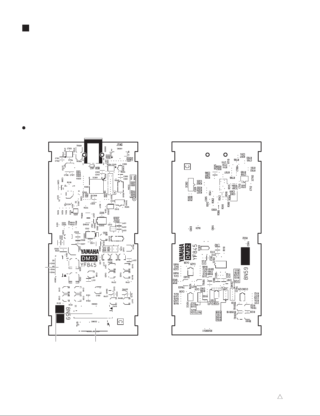
CIRCUIT BOARDS(シート基板図)
DM12 Circuit Board (YF845C0) (MG16XU) ............................................................................ 30
MAS16X (MG16XU) / MAS16 (MG16) Circuit Board (YF868C0) ....................................... 32/34
MONO16 Circuit Board (YF867B0) ..................................................................................... 36/38
PS20 Circuit Board (YF853B0) ................................................................................................. 31
Note: See parts list for details of circuit board component parts.
注 : シートの部品詳細はパーツリストをご参照ください。
DM12 Circuit Board (MG16XU)
30
(MG16XU)
to PS20-CN109
to MAS16X-CN802
(MG16XU)
to MAS16X-CN801
(MG16XU)
Component side
(部品側)
Pattern side
(パターン側)
2NA-ZH98070
2
 Loading...