

Yaesu FT-7800R Service Manual
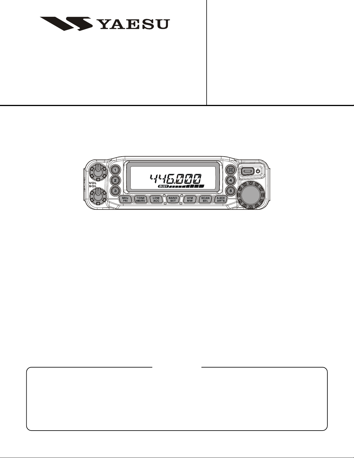
Dual Band FM Transceiver
FT-7800R
Technical Supplement
2003 VERTEX STANDARD CO., LTD. (EH016M90A
©
VERTEX STANDARD CO., LTD.
4-8-8 Nakameguro, Meguro-Ku, Tokyo 153-8644, Japan
VERTEX STANDARD
US Headquarters
10900 Walker Street, Cypress, CA 90630, U.S.A.
YAESU EUROPE B.V.
P.O. Box 75525, 1118 ZN Schiphol, The Netherlands
YAESU UK LTD.
Unit 12, Sun Valley Business Park, Winnall Close
Winchester, Hampshire, SO23 0LB, U.K.
VERTEX STANDARD HK LTD.
Unit 5, 20/F., Seaview Centre, 139-141 Hoi Bun Road,
)
Kwun Tong, Kowloon, Hong Kong
Introduction
This manual provides technical information necessary for servicing the FT-7800R Transceiver.
Servicing this equipment requires expertise in handling surface-mount chip components. Attempts by non-qualified
persons to service this equipment may result in permanent damage not covered by the warranty, and may be illegal in
some countries.
Two PCB layout diagrams are provided for each double-sided circuit board in the transceiver. Each side of thr board is
referred to by the type of the majority of components installed on that side (“leaded” or “chip-only”). In most cases one
side has only chip components, and the other has either a mixture of both chip and leaded components (trimmers, coils,
electrolytic capacitors, ICs, etc.), or leaded components only.
While we believe the technical information in this manual to be correct, Vertex Standard assumes no liability for damage that may occur as a result of typographical or other errors that may be present. Your cooperation in pointing out any
inconsistencies in the technical information would be appreciated.
Contents
Specifications ................................................ A-1
Exploded View & Miscellaneous Parts ..... B-1
Block Diagram ................................................C-1
Circuit Description ....................................... D-1
Alignment ....................................................... E-1
Board Unit (Schematics, Layouts & Parts)
MAIN Unit ................................................. F-1
PANEL Unit ............................................. G-1
CH Unit ..................................................... H-1

Specifications
General
Frequency Range: RX: 108.000 - 520.000 MHz,
700.000 - 999.995 MHz (Cellular Blocked)
TX: 144.000 - 148.000 MHz or 144.000 - 146.000 MHz,
430.000 - 450.000 MHz or 430.000 - 440.000 MHz
Channel Steps: 5/10/12.5/15/20/25/50/100 kHz
Modes of Emission: F3E, F2D, F2A
Antenna Impedance: 50 Ohms, unbalanced (Antenna Duplexer built-in)
Frequency Stability: ±5 ppm @ 14 °F ~ +140 °F (–10 °C ~ +60 °C)
Operating Temperature Range: –4 °F ~ +140 °F (–20 °C ~ +60 °C)
Supply Voltage: 13.8 VDC (±15 %), negative ground
Current Consumption (Approx.): RX: 0.5 A (Squelched)
TX: 8.5 A
Case Size (W x H x D): 5.5” x 1.6” x 6.6” (140 x 41.5 x 168 mm) (w/o knobs & connectors)
Weight (Approx.): 2.2 lb. (1 kg)
Transmitter
Output Power: 50/20/10/5 W (144 MHz)
40/20/10/5 W (430 MHz)
Modulation Type: Variable Reactance
Maximum Deviation: ±5 kHz
Spurious Radiation: At least –60 dB below
Microphone Impedance:2 kΩ
DATA Jack Impedance: 10 kΩ
Receiver
Circuit Type: Double-conversion superheterodyne
Intermediate Frequencies: 45.05 MHz/450 kHz
Sensitivity: 0.8 µV (TYP) for 10 dB SN (108 - 137 MHz, AM)
0.2 µV for 12 dB SINAD (137 - 150 MHz, FM)
0.25 µV for 12 dB SINAD (150 - 174 MHz, FM)
0.3 µV (TYP) for 12 dB SINAD (174 - 222 MHz, FM)
0.25 µV (TYP) for 12 dB SINAD (222 - 300 MHz, FM)
0.8 µV (TYP) for 10 dB SN (300 - 336 MHz, AM)
0.25 µV for 12 dB SINAD (336 - 420 MHz, FM)
0.2 µV for 12 dB SINAD (420 - 520 MHz, FM)
0.4 µV (TYP) for 12 dB SINAD (800 - 900 MHz, FM)
0.8 µV (TYP) for 12 dB SINAD (900 - 999.99 MHz, FM)
Squelch Sensitivity: Better than 0.16 µV
Selectivity (–6dB/–60dB): 12 kHz/30 kHz
Maximum AF Output: 2 W @ 8 Ω for 10% THD
AF Output Impedance: 4-16 Ω
Specifications are subject to change without notice, and are guaranteed within the 144 and 430 MHz amateur bands only. Frequency
ranges will vary according to transceiver version; check with your dealer.
A-1
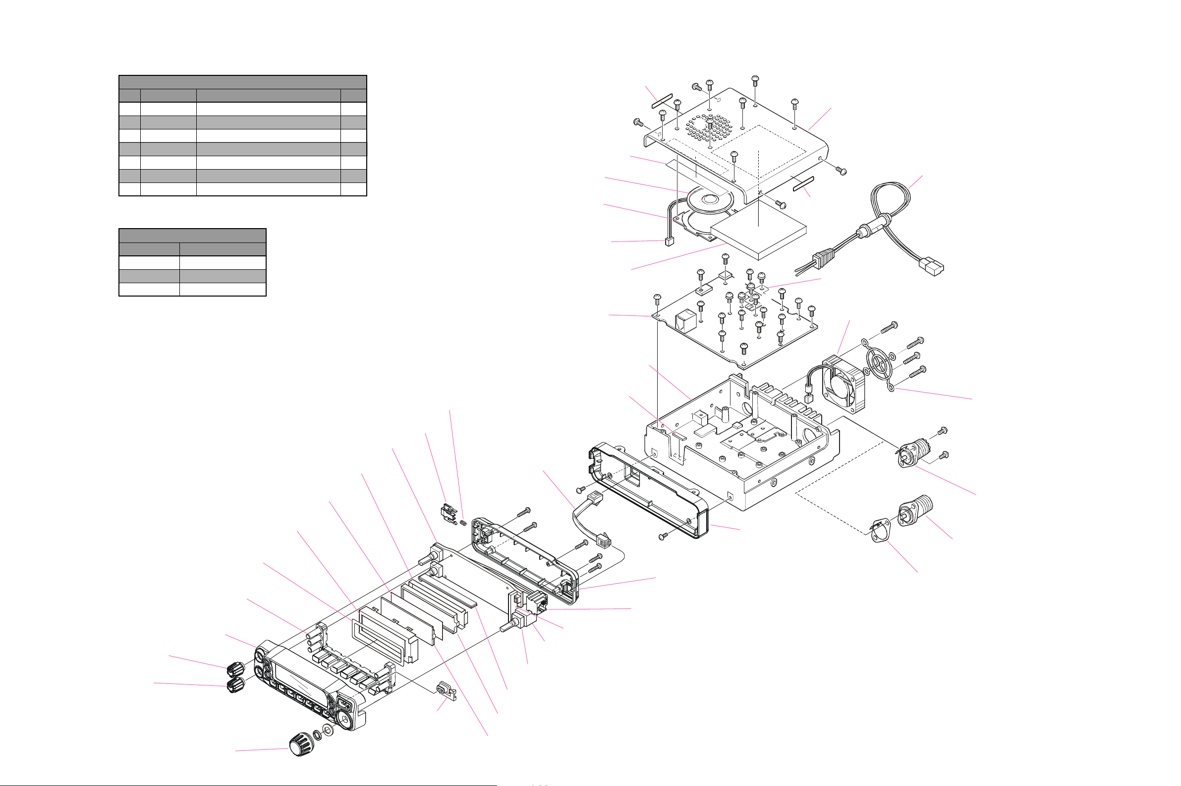
Exploded View & Miscellaneous Parts
SCREW LIST
No. VXSTD P/N DESCRIPTION QTY.
U31208007 OVAL HEAD SCREW M2.6X8B 8
U44308002 TAPTITE SCREW M3X8NI 17
U03310002 SEMS SCREW ASM3X10NI 4
U20308002 BINDING HEAD SCREW M3X8NI 2
U25320007 TAPTITE SCREW M3X20B 4
U23116007 TAPTITE SCREW M2X16B 5
U31206007 OVAL HEAD SCREW M2.6X6B 6
SUPPLIED ACCESSORIES
VXSTD P/N DESCRIPTION
Q0000081 FUSE 15A (x2 pcs)
AAA43X001 MIC MH-48A6J
T9021715 DC CABLE
R8139500
LABEL
RA02132A0
HIMERON TAPE
M4090149
SPEAKER
R0150630
HOLDER
T9206438A
WIRE ASSY
RA0322600
RUBBER SHEET
MAIN UNIT
RA02668AA
CHASSIS
CS1804001
CASE (W/ NYLON NET)
R8139500
LABEL
RA0415200 (x2 pcs)
GROUND PLATE
M2090034A
FAN
T9206876
WIRE ASSY
RA0552200
LCD SPACER
RA0539900
RUBBER KNOB
RA0541400
FRONT PANEL ASSY
(W/ WINDOW, DOUBLE FACE TAPE)
RA0540200
KNOB
RA0540200
KNOB
RA0540100
ENCODER KNOB
RA0551900
REFLECTOR SHEET
RA0551800
DIFFUSER SHEET
RA0540800
LCD HOLDER
PANEL UNIT
*
*
RA0022900
COIL SPRING
RA0540400
RELEASE KNOB
RA0540300
KNOB
T9101536
CT CABLE
Q9000804
ROTARY ENCODER (W/ HEX NUT*, WASHER*)
RA0540900
INTER CONNECTOR
RA0540700
LIGHT GUIDE
G6090155
LCD
RA0438700
RUBBER
CH UNIT
P1091107
CONNECTOR
RA0551700
REAR PANEL ASSY
(W/ COIL SPRING, RELEASE KNOB)
T9207057
WIRE ASSY
RA0539800
SUB PANEL
S5000206
FAN GUARD
P1090984
CONNECTOR (Ver: USA)
P1090547
CONNECTOR (Ver: EXP, AUS)
S5000236
WASHER (Ver: EXP, AUS)
Non-designated parts are available only
as part of a designated assembly.
B-1

Exploded View & Miscellaneous Parts
Note
B-2
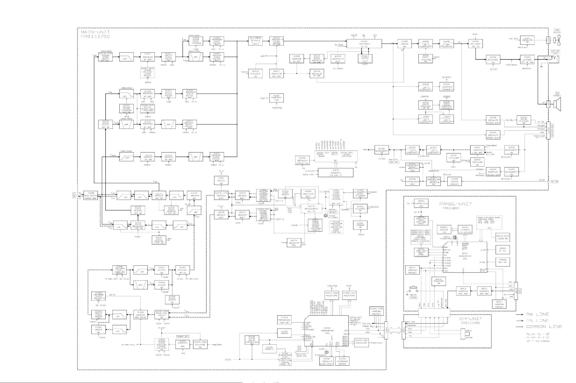
Block Diagram
D-1

Block Diagram
Note
D-2

Circuit Description
VHF Reception
The incoming VHF signal is passed through a low-pass
filter network, antenna switching diodes D1074 (RLS135),
D1075 (RLS135) and D1015 (HVC131), and another low-
pass filter network to the RF amplifier Q1008 (3SK296ZQ).
The amplified RF signal is passed through a varactor controlled bandpass filter consisting of L1017, L1018, and
D1010, D1011, and D1012 (all HVC365), then applied to
the first mixer Q1009 (3SK296ZQ) along with the first
local signal from the PLL circuit.
The first local signal is generated between 189.05 MHz
and 193.05 MHz, depending on the receiving frequency,
by the VHF VCO, which consists of Q1076 (2SC5374) and
varactor diodes D1049 (HVC365), D1050 (HVC131),
D1051 (HVC365), and D1052 (HVC362).
UHF Reception
The incoming UHF signal is passed through a low-pass
filter network, antenna switching diodes D1077
(UM9401F) and D1018 (RLS135), D1019 (RLS135), and
D1084 (HSC277), and another low-pass filter network to
the RF amplifier Q1001 (3SK296ZQ). The amplified RF
signal is passed through a varactor-controlled band-pass
filter consisting of L1006 and L1007, and D1002, D1003,
and D1004 (all HVC350B), then applied to the first mixer
Q1002 (3SK296ZQ) along with the first local signal from
the PLL circuit.
The first local signal is generated between 384.95 MHz
and 404.95 MHz, depending on the receiving frequency,
by the UHF VCO, which consists of Q1072 (2SC5006)
and varactor diodes D1046 (HVC375B) and D1047
(HVC350B).
IF and Audio Circuits
The 45.05 MHz first IF signal is applied to the monolithic
crystal filter XF1001 which strips away unwanted mixer
products, and the IF signal is applied to the first IF amplifier Q1016 (2SC4400). The amplified first IF signal is then
delivered to the FM IF subsystem IC Q1023 (TA31136FN),
which contains the second mixer, limiter amplifier, noise
amplifier, and FM detector.
The 44.6 MHz second local signal is derived from 11.15
MHz crystal X1002, the frequency of which is multiplied
by four at Q1022 (2SC4400), producing the 450 kHz sec-
ond IF signal when mixed with the first IF signal within
Q1023 (TA31136FN).
The detected audio passes through the de-emphasis network, a low-pass filter consisting of Q1028 (NJM2902V)
and associated circuitry, and a high-pass filter consisting
of Q1028 (NJM2902V) and associated circuitry. The filtered audio signal is passed through the audio volume
control IC Q1034 (M51132FP) which adjusts the audio
sensitivity to compensate for audio level variations, then
delivered to the audio switch Q1036 (DTC144EE).
Squelch Control
When no carrier received, noise at the output of the detector stage in Q1023 (TA31136FN) is amplified and bandpass filtered by the noise amp section of Q1023
(TA31136FN). The resulting DC voltage is applied to pin
2 of main CPU Q1065 (M3826AEFGP), which compares
the squelch threshold level to that which set by the front
panel SQL knob.
While no carrier is received, pin 53 of Q1065
(M3826AEFGP) remains “low,” to disable audio output
from the speaker.
Transmit Signal Path
The speech signal from the microphone passes through
the MIC jack J2001 to AF amplifier Q2011 (NJM2904V)
on the PANEL unit. The amplified speech signal is subjected to amplitude limiting by Q1040 (NJM2902V) on
the MAIN unit. The speech signal then passes through
low-pass filter network Q1040 (NJM2902V) and band
switch Q1039 (BU4066BCFV) to the VHF VCO or UHF
VCO.
VHF Transmit Signal Path
The adjusted speech signal from Q1040 (NJM2902V) is
delivered to VHF VCO Q1076 (2SC5374) which frequen-
cy modulates the transmitting VCO made up of D1049
(HVC365). The modulated transmit signal passes through
buffer amplifiers Q1077 and Q1078 (both 2SC5374). The
amplified transmit signal is then applied to the Pre-Drive
amplifier Q1084 (2SK2596) and Driver amplifier Q1086
(RD07MVS1), then finally amplified by Power amplifier
Q1087 (RD70HVF1) up to 50 Watts. This three-stage pow-
er amplifier’s gain is controlled by the APC circuit. The
50 Watt RF signal passes through high-pass filter and lowpass filter network, antenna switch D1072 and D1073
(both XB15A709A), and another low-pass filter network,
and then is delivered to the ANT jack.
The 450 kHz second IF signal is applied to the ceramic
filter CF1001 which strips away all but the desired shignal, and then passes through the limiter amplifier within
Q1023 (TA31136FN) to the ceramic discriminator CD1001
which removes any amplitude variations in the 450 kHz
IF signal before detection of speech.
D-1

Circuit Description
UHF Transmit Signal Path
The adjusted speech signal from Q1040 (NJM2902V) is
delivered to UHF VCO Q1072 (2SC5006) which frequency modulates the transmitting VCO made up of D1046
(HVC375B). The modulated transmit signal passes
through buffer amplifiers Q1073, Q1074, and Q1075 (all
2SC5006). The filtered transmit signal is then applied to
the Pre-Drive amplifier Q1084 (2SK2596) and Driver amplifier Q1086 (RD07MVS1), then finally amplified by Power amplifier Q1087 (RD70HVF1) up to 40 Watts. This
three-stage power amplifier’s gain is controlled by the
APC circuit. The 40 Watt RF signal passes through highpass filter and low-pass filter networks, antenna switch
D1077 (UM9401F), and another low-pass filter network,
and then is delivered to the ANT jack.
TX APC Circuit
A portion of the power amplifier output is rectified by
D1070 and D1071 (UHF: D1078 and D1079, all
MA2S728), then delivered to APC Q1081 (NJM2904V),
as a DC voltage which is proportional to the output level
of the power amplifier. The APC Q1081 (NJM2904V) com-
pares the rectified DC voltage from the power amplifier
and the reference voltage from the main CPU Q1065
(M3826AEFGP), to produce a control voltage, which regulates supply voltage to the Pre-Drive amplifier Q1084
(2SK2596), Drive amplifier Q1086 (RD07MVS1) and
Power amplifier Q1087 (RD70HVF1), so as to maintain
stable output power under varying antenna loading conditions.
PTT Circuit
When the PTT switch is pressed, pin 8 of sub CPU Q2001
(M38223E) goes “high”, which send the “PTT” command
to main CPU Q1065 (M3826AEFGP). When the CPU receives the “PTT” command, it engages Q1057 (UMA8N)
and Q1058 (IMT17), which activates the Tx circuit.
PLL Circuit
A portion of the output from the VCO Q1076 (2SC5374)
and Q1072 (2SC5006), passes through the programmable divider section of the PLL IC Q1070 (MB15A02PFV1),
which divides the VCO frequency according to the frequency dividing data that is associated with the current
frequency input from the main CPU Q1065
(M3826AEFGP). It is then sent to the phase comparator.
The 11.15 MHz frequency of the reference oscillator circuit derived from X1002 is divided by the reference frequency divider section of Q1070 (MB15A02PFV1) into
4250 or 3400 parts to become 5 kHz or 6.25 kHz comparative reference frequencies, which are utilized by the phase
comparator. The phase comparator section of Q1070
(MB15A02PFV1) compares the phase between the frequency-divided oscillation frequency of the VCO circuit
and the comparative frequency and its output is a pulse
corresponding to the phase difference. This pulse is integrated by the charge pump and loop filter of Q1070
(MB15A02PFV1) into a control voltage (VCV) to control
the oscillation frequency of the VCOs.
D-2
Alignment
Introduction and Precautions
The FT-7800R has been carefully aligned at the factory
for the specified performance across the 144 MHz and 430
MHz amateur bands. Realignment should therefore not
be necessary except in the event of a component failure.
All component replacement and service should be performed only by an authorized Vertex Standard representative, or the warranty policy may be voided.
The following procedures cover the sometimes critical and
tedious adjustments that are not normally required once
the transceiver has left the factory. However, if damage
occurs and some parts are replaced, realignment may be
required. If a sudden problem occurs during normal operation, it is likely due to component failure; realignment
should not be done until after the faulty component has
been replaced.
We recommend that servicing be performed only by authorized Vertex Standard service technicians who are experienced with the circuitry and fully equipped for repair and alignment. Therefore, if a fault is suspected, contact the dealer from whom the transceiver was purchased
for instructions regarding repair. Authorized Vertex Standard service technicians realign all circuits and make complete performance checks to ensure compliance with factory specifications after replacing any faulty components.
Those who do undertake any of the following alignments
are cautioned to proceed at their own risk. Problems
caused by unauthorized attempts at realignment are not
covered by the warranty policy. Also, Vertex Standard
must reserve the right to change circuits and alignment
procedures in the interest of improved performance, without notifying owners.
Under no circumstances should any alignment be attempted unless the normal function and operation of the transceiver are clearly understood, the cause of the malfunction has been clearly pinpointed and any faulty components replaced, and the need for realignment determined
to be absolutely necessary.
Required Test Equipment
The following test equipment (and thorough familiarity
with its correct use) is necessary for complete realignment.
Correction of problems caused by misalignment resulting from use of improper test equipment is not covered
under the warranty policy. While most steps do not require all of the equipment listed, the interactions of some
adjustments may require that more complex adjustments
be performed afterwards. Do not attempt to perform only
a single step unless it is clearly isolated electrically from
all other steps. Have all test equipment ready before beginning, and follow all of the steps in a section in the order presented.
Regulated DC Power Supply: adjustable from 11.5 to
16 VDC, 10 A
RF Signal Generator with calibrated output level at
500 MHz
Frequency Counter: ±0.1 ppm accuracy at 500 MHz
AF Signal Generator
SINAD Meter
Oscilloscope
Spectrum Analyzer
Deviation Meter (linear detector)
AF Millivoltmeter
AF Dummy Load: 8-Ohm, 5 W
DC Voltmeter: high impedance
Inline Wattmeter with 5% accuracy at 500 MHz
50-Ohm non-reactive Dummy Load: 50 watts at 500 MHz
VHF/UHF Sampling Coupler
Set up the test equipment as shown below, and apply 13.8
VDC power to the transceiver.
SINAD
Meter
8-ohm
Dummy Load
EXT SP
Power Supply
13.8 VDC
RF Signal
Generator
RF Sampling
Coupler
Inline
Wattmeter
50-ohm
Dummy Load
Frequency
Counter
Pin 5
Deviation
Meter
AF Signal
Generator
E-1
Alignment
Alignment Preparation & Precautions
A dummy load and inline wattmeter must be connected
to the main antenna jack in all procedures that call for
transmission, except where specified otherwise. Correct
alignment is not possible with an antenna. After completing one step, read the following step to determine whether the same test equipment will be required. If not, remove the test equipment (except dummy load and wattmeter, if connected) before proceeding.
Correct alignment requires that the ambient temperature
in the repair shop be the same as that of the transceiver
and test equipment, and that this temperature be held
constant between 68 °C and 86 °F (20 °C ~ 30 °C). When
the transceiver is brought into the shop from hot or cold
air it should be allowed some time for thermal equalization with the environment before alignment. If possible,
alignments should be made with oscillator shields and
circuit boards firmly affixed in place. Also, the test equipment must be thoroughly warmed up before beginning.
Notes: Signal levels in dB referred to in alignment are
based on 0 dBµ = 0.5 µV (closed circuit).
Entering the Alignment mode
Alignment of the FT-7800R is performed using a frontpanel software-based procedure. To perform alignment
of the transceiver, it must first be placed in the “Alignment Mode,” in which the adjustments will be made and
then stored into memory.
To enter the Alignment mode:
1. Press and hold in the [MHz(PRI)] key and the Hyper
Memory [5] key while turning the radio on. Once the
radio is on, release these two keys.
2. Press the front panel keys in the following sequence.
[
MHz(PRI)] [TONE(HM/RV)] [LOW(ACC)]
[
BAND(SET)] [V/M(MW)]
[
SCAN(SEL)] [S.SCH(ARTS
3. Press and hold in the
REF.xxH” to appear on the display, this signifies that
the transceiver is now in the “Alignment mode.”
[ ]
key to cause “A-0
)]
PLL Reference Frequency
1. Tune the frequency to 435.050 MHz, then set the Transmit Power Level to “LOW.”
2. Press the [BAND(SET)] key while pressing and holding in the
parameter to “A-0 REF.xxH.”
3. Press the PTT switch to activate the transmitter, and
adjust the DIAL knob while pressing and holding the
]
[
key, if needed, so that the counter frequency read-
ing is 435.050 MHz (±100 Hz).
[ ]
key, if needed, to set the Alignment
RF Front-end Tuning
1. Connect the DC voltmeter to TP1010 on the MAIN
Unit, then inject a 439.050 MHz signal at a level of +10
dBµ (with 1 kHz modulation @±3.5 kHz deviation)
from the RF Signal Generator.
2. Tune the frequency to 439.050 MHz.
3. Press the [BAND(SET)] key while pressing and holding the
“A-1 TUN.xxH.”
4. Adjust the DIAL knob while pressing and holding in
the
reaches maximum deflection. The FT-7800R’s RF
Front-end has a broad bandwidth. Therefore, prior to
adjustment you must adjust the DIAL knob to set the
frequency to the middle of the band, in step 2, so you
can set peak in the DC voltmeter's deflection in the
center of the RF passband.
5. Tune the frequency to 145.050 MHz.
6. Inject a 145.050 MHz signal at a level of +10 dBµ (with
1 kHz modulation @±3.5 kHz deviation) from the RF
Signal Generator.
7. Adjust the DIAL knob while pressing and holding in
the
reaches maximum deflection. As in the previous section, be sure to set the DIAL knob for the center of the
band prior to making this adjustment.
[ ]
key to set the Alignment parameter to
[ ]
key, if needed, so that the DC voltmeter
[ ]
key, if needed, so that the DC voltmeter
TP1010
E-2
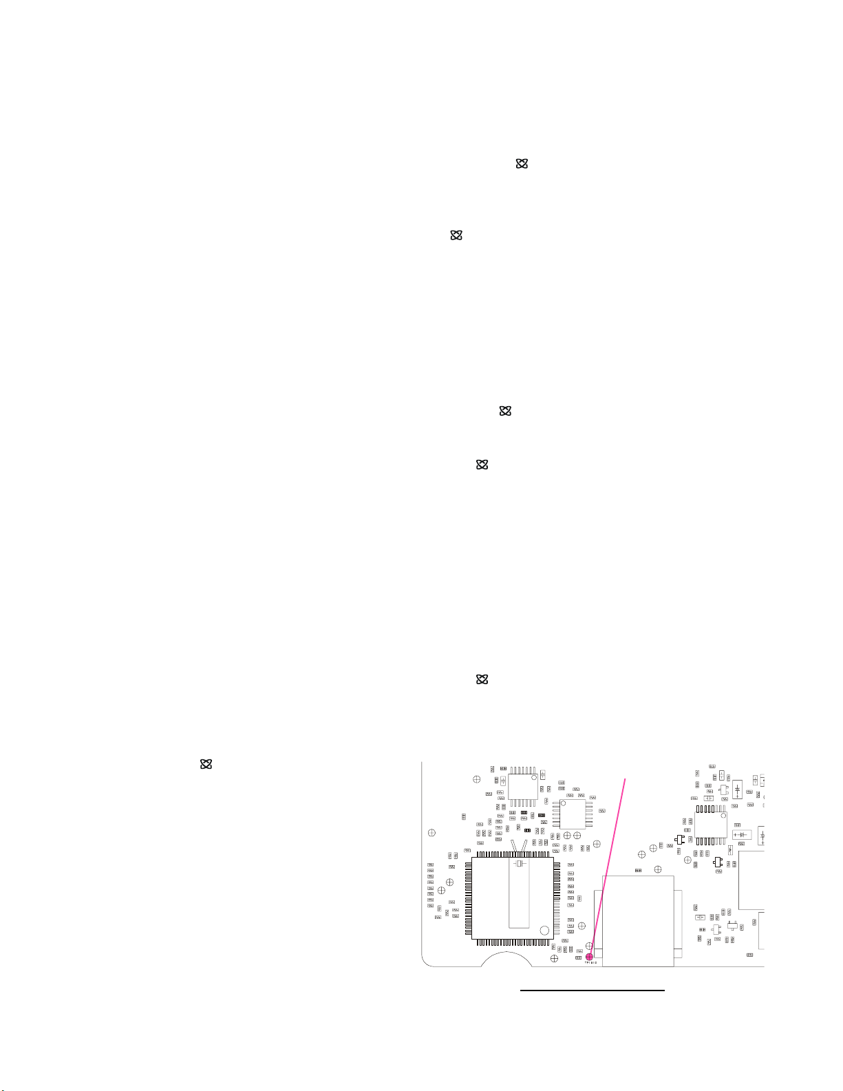
MAIN UNIT TEST POINTS

Alignment
TX Power Output
1. Tune the frequency to 440.050 MHz, then set the Transmit Power Level to “LOW.”
2. Press the [BAND(SET)] key while pressing and holding in the
“A-2 PWR.xxH.”
3. Press the PTT switch to activate the transmitter, and
adjust the DIAL knob while pressing and holding in
the
is 5 Watts (±0.5 Watt).
4. Increase the Transmit Power Level to “MID2.”
5. Press the PTT switch to activate the transmitter, and
adjust the DIAL knob while pressing and holding in
the
is 10 Watts (±0.5 Watt).
6. Increase the Transmit Power Level to “MID1.”
7. Press the PTT switch to activate the transmitter, and
adjust the DIAL knob while pressing and holding in
the
is 20 Watts (±0.5 Watt).
8. Increase the Transmit Power Level to “HIGH.”
9. Press the PTT switch to activate the transmitter, and
adjust the DIAL knob while pressing and holding in
the
is 40 Watts (±0.5 Watt).
10. Tune the frequency to 146.050 MHz, then set the Transmit Power Level to “LOW.”
11. Press the PTT switch to activate the transmitter, and
adjust the DIAL knob while press and holding the [%]
key, as needed, so that the wattmeter reading is 5 Watts
(±0.5 Watt).
12. Increase the Transmit Power Level to “MID2.”
13. Press the PTT switch to activate the transmitter, and
adjust the DIAL knob while pressing and holding in
the
is 10 Watts (±0.5 Watt).
14. Increase the Transmit Power Level to “MID1.”
15. Press the PTT switch to activate the transmitter, and
adjust the DIAL knob while pressing and holding in
the
is 20 Watts (±0.5 Watt).
16. Increase the Transmit Power Level to “HIGH.”
17. Press the PTT switch to activate the transmitter, and
adjust the DIAL knob while pressing and holding in
the
is 50 Watts (±0.5 Watt).
[ ]
key to set the Alignment parameter to
]
[
key, if needed, so that the wattmeter reading
[
]
key, if needed, so that the wattmeter reading
[ ]
key, if needed, so that the wattmeter reading
[ ]
key, if needed, so that the wattmeter reading
[ ]
key, if needed, so that the wattmeter reading
[ ]
key, if needed, so that the wattmeter reading
[ ]
key, if needed, so that the wattmeter reading
TX Deviation
1. Tune the frequency to 440.050 MHz, then set the Transmit Power Level to “LOW.”
2. Press the [BAND(SET)] key while pressing and holding in the
“A-3 DEV.xxH.”
3. Inject a 1 kHz audio tone at a level of 80 mV (–20 dBm)
from the Audio Generator.
4. Press the PTT switch to activate the transmitter, and
adjust the DIAL knob while pressing and holding in
the
reading is 4.2 kHz (±0.2 kHz) (EXP Version: 4.5 kHz
(±0.2 kHz)).
5. Tune the frequency to 146.050 MHz, then set the Transmit Power Level to “LOW.”
6. Press the PTT switch to activate the transmitter, and
adjust the DIAL knob while pressing and holding in
the
reading is 4.2 kHz (±0.2 kHz) (EXP Version: 4.5 kHz
(±0.2 kHz)).
[ ]
key to set the Alignment parameter to
[ ]
key, if needed, so that the deviation meter
[ ]
key, if needed, so that the deviation meter
DCS TX Deviation
1. Tune the frequency to 440.050 MHz, then activate the
DCS with a “023” DCS code, and set the Transmit
Power Level to “LOW.”
2. Press the [BAND(SET)] key while pressing and holding in the
“A-4 DSC.xxH.”
3. Press the PTT switch to activate the transmitter (with
no microphone input), and adjust the DIAL knob while
pressing and holding in the
the deviation meter reading is between 0.50 kHz and
0.60 kHz.
4. Tune the frequency to 146.050 MHz, then activate the
DCS with a “023” DCS code, and set the Transmit
Power Level to “LOW.”
5. Press the PTT switch to activate the transmitter (with
no microphone input), and adjust the DIAL knob while
pressing and holding in the
the deviation meter reading is between 0.50 kHz and
0.60 kHz.
[ ]
key to set the Alignment parameter to
[ ]
key, if needed, so that
[ ]
key, if needed, so that
E-3

Alignment
CTCSS TX Deviation
1. Tune the frequency to 440.050 MHz, then activate the
CTCSS Encoder with a “100 Hz” tone, and set the
Transmit Power Level to “LOW.”
2. Press the [BAND(SET)] key while press and holding
]
[
the
CTC.xxH.”
3. Press the PTT switch to activate the transmitter (with
no microphone input), and adjust the DIAL knob
while pressing and holding in the
so that the deviation meter reading is between 0.65
kHz and 0.75 kHz.
4. Tune the frequency to 146.050 MHz, then activate the
CTCSS Encoder with a “100 Hz” tone, and set the
Transmit Power Level to “LOW.”
5. Press the PTT switch to activate the transmitter (with
no microphone input), and adjust the DIAL knob while
pressing and holding in the
the deviation meter reading is between 0.65 kHz and
0.75 kHz.
key to set the Alignment parameter to “A-5
[
]
key, if needed,
[ ]
key, if needed, so that
Center Meter Sensitivity
1. Tune the frequency to 440.050 MHz.
2. Press the [BAND(SET)] key while press and holding
[ ]
the
CNTL/V.”
3. Inject a 1 kHz audio tone at a level of +10 dBµ from
the Audio Generator.
4. Press the [LOW(ACC)] key while press and holding
the
key to set the Alignment parameter to “A-6
[ ]
key.
7. Tune the frequency to 146.050 MHz.
8. Inject a 146.050 MHz signal at a level of –5 dBµ (with
1 kHz modulation @±3.5 kHz deviation) from the RF
Signal Generator.
9. Press the [LOW(ACC)] key while pressing and hold-
[ ]
[ ]
[ ]
[ ]
key.
[ ]
key.
[ ]
key.
key.
key.
key.
ing in the
10. Increase the RF Signal Generator output level to +23
dBµ.
11. Press the [V/M(MW)] key while pressing and holding
in the
12. Tune the frequency to 230.050 MHz.
13. Inject a 230.050 MHz signal at a level of –5 dBµ (with
1 kHz modulation @±3.5 kHz deviation) from the RF
Signal Generator.
14. Press the [LOW(ACC)] key while pressing and holding in the
15. Increase the RF Signal Generator output level to +23
dBµ.
16. Press the [V/M(MW)] key while pressing and holding
in the
17. Tune the frequency to 850.050 MHz.
18. Inject a 850.050 MHz signal at a level of +3 dBµ (with
1 kHz modulation @±3.5 kHz deviation) from the RF
Signal Generator.
19. Press the [LOW(ACC)] key while pressing and holding in the
20. Increase the RF Signal Generator output level to +31
dBµ.
21. Press the [V/M(MW)] key while pressing and holding
in the
S-Meter Sensitivity
1. Tune the frequency to 440.050 MHz.
2. Press the [BAND(SET)] key while press and holding
[ ]
the
SM L/V.”
3. Inject a 440.050 MHz signal at a level of –5 dBµ (with
1 kHz modulation @±3.5 kHz deviation) from the RF
Signal Generator.
4. Press the [LOW(ACC)] key while pressing and hold-
ing in the
5. Increase the RF Signal Generator output level to +23
dBµ.
6. Press the [V/M(MW)] key while pressing and holding
in the
key to set the Alignment parameter to “A-7
[ ]
key.
[ ]
key.
DC Voltmeter
1. Set the power supply voltage to 13.8 VDC.
2. Press the [BAND(SET)] key while pressing and holding in the
“A-8 BAT SC.”
3. Press the [SCAN(SEL)] key.
To close the Alignment mode, just press and hold in the
PWR switch for 0.5 seconds (to turn the power off). The
next time the transceiver is turned on, normal operation
may resume.
[ ]
key to set the Alignment parameter to
E-4

MAIN Unit
[–4.3 dBµ]
0.81 V
[+1.4 dBµ]
2.22 V
(–6.2 dBµ)
[+18.8 dBµ]
(+15.8 dBµ)
0.97 V
1.37 V
0.78 V
0.30 V
0.15 V
(+0.8 dBµ)
8.13 V
0.32 V
8.56 V
8.83 V
8.53 V
8.57 V
0.71 V
0.70 V
8.70 V
0.69 V
4.94 V
0.98 V
2.92 V
0.71 V
4.75 V
[+15.9 dBµ]
[+15.5 dBµ]
1.10 V
4.69 V
1.56 V
1.48 V
0.43 V
0.50 V
5.83 V
45.05 MHz
(+21.6 dBµ)
[+21.0 dBµ]
1.23 V
2.22 V
2.09 V
0.68 V
0.23 V
45.05 MHz
(+12.3 dBµ)
[+11.6 dBµ]
0.83 V
0.82 V
0.13 V
0.71 V
0.11 V
0.69 V
4.94 V
4.72 V
45.05 MHz
(+23.4 dBµ)
[+22.6 dBµ]
Q1023
Pin 1: 4.79 V
Pin 4: 4.81 V
Pin 8: 0.65 V
Pin 10: 4.81 V
AM: 3.74 V
Q1034
1.42 V
1.89 V
8.65 V
AM: 2.03 V
8.82 V
1.10 V
AM: 3.35 V
0.91 V
2.33 V
1.88 V
8.87 V
0 V
2.00 V 2.00 V
2.00 V
1.78 V
1.78 V
2.01 V
2.00 V
0.93 V
8.80 V
8.86 V
2.33 V
1.91 V
4.98 V
1.89 V
8.86 V
Pin 2: 8.33 V
Pin 14: 8.40 V
Pin 15: 3.57 V
Pin 16: 3.27 V
Circuit Diagram
0 ~ 4.90 V
13.78 V
1.40 V
4.86 V
7.00 V
(–8.6 dBµ)
[–9.2 dBµ]
(12.60 V)
[12.54 V]
(11.45 V)
[11.23 V]
(12.73 V)
[12.76 V]
(3.25 V)
[3.62 V]
(3.55 V)
[3.30 V]
4.67 V
6.68 V
8.17 V
4.86 V
4.97 V
4.90 V
5.00 V
5.65 V
4.98 V
4.98 V
4.95 V
8.95 V
5.00 V
5.00 V
0.70 V
13.78 V
13.05 V
13.80 V
0.12 V
4.56 V
(xxx): Freq. = 146.05 MHz
[xxx]: Freq. = 440.05 MHz
(xxx): Freq. = 146.05 MHz
[xxx]: Freq. = 440.05 MHz
F-1

MAIN Unit
Note
F-2
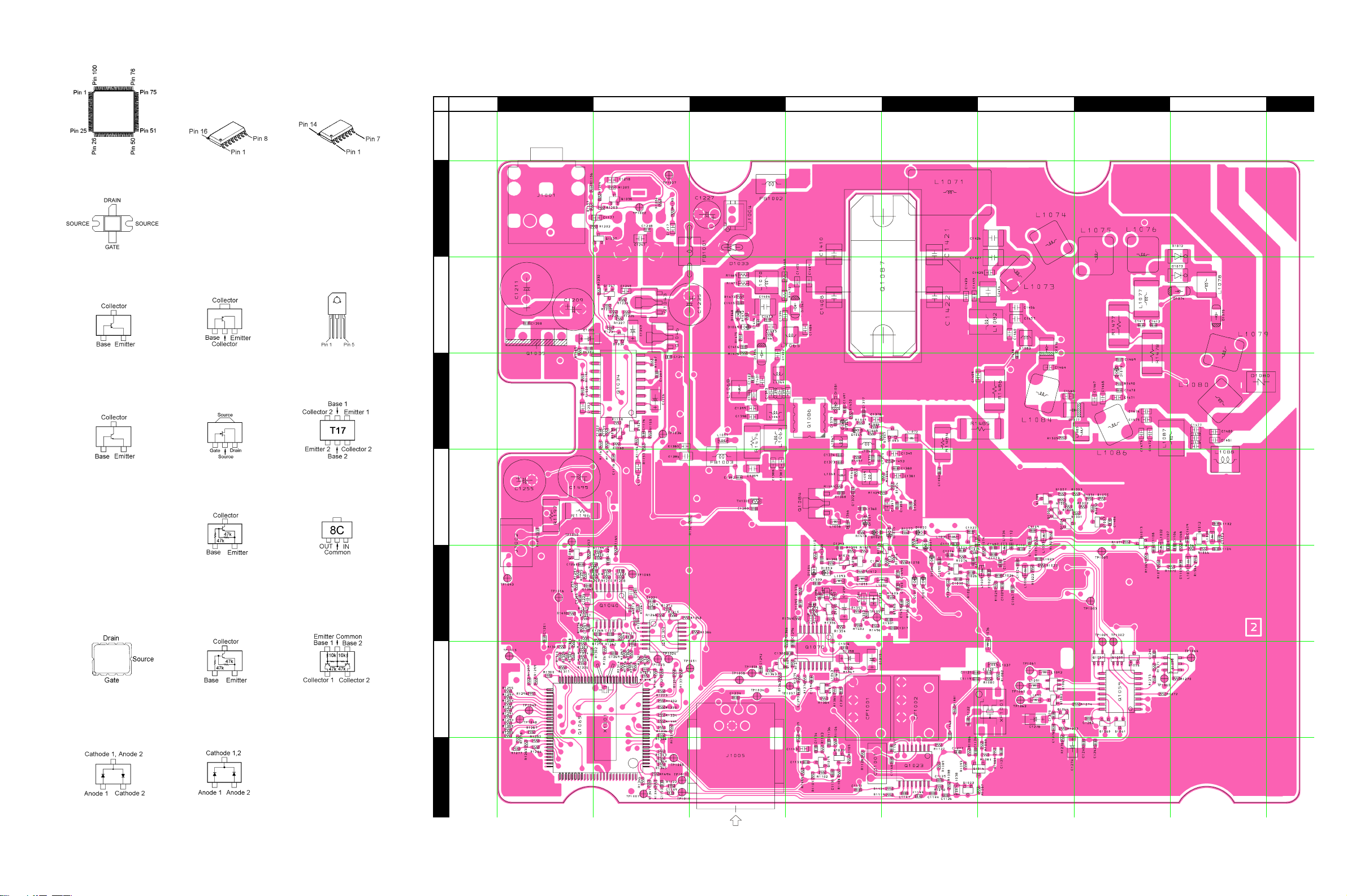
MAIN Unit
Parts Layout (Side A)
A B C D E F G H I
M3826AEFGP
(Q1065)
RD70HVF1
(Q1087)
2SA1774 (FR)
(Q1069)
2SC4400 (RT4)
(Q1016)
2SC4617 (BR)
(Q1019, 1020, 1029,
1030, 1047, 1064,
1071)
2SC5006 (24)
(Q1003, 1013, 1014,
1074, 1075)
2SC5277 (D2)
(Q1012)
2SC5374 (NA)
(Q1078)
BU2090FS
(Q1059)
M51132FP
(Q1034)
MB15A022PFV1
(Q1070)
TA31136FN
(Q1023)
2SB1301 (ZQ)
(Q1043)
2SK2596 (BX)
(Q1084)
DTA144EE (16)
(Q1056, 1062)
BU4066BCFV
(Q1039)
NJM2902V
(Q1040)
1
2
LA4425A
(Q1035)
3
IMT17 (T17)
(Q1058)
4
NJM78L05 (8C)
(Q1046)
5
RD07MVS1
(Q1086)
DA221 (K)
(D1040)
DTC144EE (26)
(Q1037, 1038, 1054,
1068)
DAN222 (N)
(D1022, 1063)
UMA8N (A8)
(Q1055, 1057, 1063)
6
7
F-3
 Loading...