

Page 1

PowerPC™ 405 Processor
Block Reference Guide
Embedded Development Kit
UG018 (v2.0) August 20, 2004
R
Page 2
R
"Xilinx" and the Xilinx logo shown above are registered trademarks of Xilinx, Inc. Any rights not expressly granted herein are reserved.
CoolRunner, RocketChips, Rocket IP, Spartan, StateBENCH, StateCAD, Virtex, XACT, XC2064, XC3090, XC4005, and XC5210 are
registered trademarks of Xilinx, Inc.
The shadow X shown above is a trademark of Xilinx, Inc.
ACE Controller, ACE Flash, A.K.A. Speed, Alliance Series, AllianceCORE, Bencher, ChipScope, Configurable Logic Cell, CORE Generator,
CoreLINX, Dual Block, EZTag, Fast CLK, Fast CONNECT, Fast FLASH, FastMap, Fast Zero Power, Foundation, Gigabit Speeds...and
Beyond!, HardWire, HDL Bencher, IRL, J Drive, JBits, LCA, LogiBLOX, Logic Cell, LogiCORE, LogicProfessor, MicroBlaze, MicroVia,
MultiLINX, NanoBlaze, PicoBlaze, PLUSASM, PowerGuide, PowerMaze, QPro, Real-PCI, RocketIO, SelectIO, SelectRAM, SelectRAM+,
Silicon Xpresso, Smartguide, Smart-IP, SmartSearch, SMARTswitch, System ACE, Testbench In A Minute, TrueMap, UIM, VectorMaze,
VersaBlock, VersaRing, Virtex-II Pro, Virtex-II EasyPath, Virtex-4, Virtex-4-FX, Wave Table, WebFITTER, WebPACK, WebPOWERED,
XABEL, XACT-Floorplanner, XACT-Performance, XACTstep Advanced, XACTstep Foundry, XAM, XAPP, X-BLOX +, XC designated
products, XChecker, XDM, XEPLD, Xilinx Foundation Series, Xilinx XDTV, Xinfo, XSI, XtremeDSP and ZERO+ are trademarks of Xilinx,
Inc.
The Programmable Logic Company is a service mark of Xilinx, Inc.
All other t rademarks are the property of their respective owners.
Xilinx, Inc. does not assume any liability arising out of the application or use of any product described or shown herein; nor does it convey
any license under its patents, copyrights, or maskwork rights or any rights of others. Xilinx, Inc. reserves the right to make changes, at any
time, in order to improve reliability, function or design and to supply the best product possible. Xilinx, Inc. will not assume responsibility for
the use of any circuitry described herein other than circuitry entirely embodied in its products. Xilinx provides any design, code, or
information shown or described herein "as is." By providing the design, code, or information as one possible implementation of a feature,
application, or standard, Xilinx makes no representation that such implementation is free from any claims of infringement. You are
responsible for obtaining any rights you may require for your implementation. Xilinx expressly disclaims any warranty whatsoever with
respect to the adequacy of any such implementation, including but not limited to any warranties or representations that the implementation
is free from claims of infringement, as well as any implied warranties of merchantability or fitness for a particular purpose. Xilinx, Inc. devi ces
and products are protected under U.S. Patents. Other U.S. and foreign patents pending. Xilinx, Inc. does not represent that devices shown
or products described herein are free from patent infringement or from any other third party right. Xilinx, Inc. assumes no obligation to
correct any errors contained herein or to advise any user of this text of any correction if such be made. Xilinx, Inc. will not assume any liability
for the accuracy or correctness of any engineering or software support or assistance provided to a user.
Xilinx products are not intended for use in life support appliances, devices, or systems. Use of a Xilinx product in such applications without
the written consent of the appropriate Xilinx officer is prohibited.
The contents of this manual are owne d and copyrigh ted by Xilinx . C opyright 1994-2004 Xilinx, Inc. All Rights Reserved. Except as stated
herein, none of the material may be copied, reproduced, distributed, republished, downloaded, displayed, posted, or transmitted in any form
or by any means including, but not limited to, electronic, mechanical, photocopying, recording, or otherwise, without the prior written cons ent
of Xilinx. Any unauthorized use of any material contained in this manual may violate copyright laws, trademark laws, the laws of privacy and
publicity, and communications regulations and statutes.
PowerPC™ 405 Processor Block Reference Guide www.xilinx.com UG018 (v2.0) August 20, 2004
1-800-255-7778
Page 3
PowerPC™ 405 Processor Block Reference Guide
UG018 (v2.0) August 20, 2004
The following table shows the revision history for this document.
Version Revision
09/16/02 1.0 Initial Embedded Development Kit (EDK) release.
09/02/03 1.1 Updated for EDK 6.1 release
04/26/04 DRAFT Early Access release (DRAFT).
06/15/04 DRAFT Second Early Access release (DRAFT).
08/20/04 2.0 Updated to include Virtex-4 functionality.
UG018 (v2.0) August 20 , 20 04 www.xilinx.com PowerPC™ 405 Processor Block Reference Gu id e
1-800-255-7778
Page 4

PowerPC™ 405 Processor Block Reference Guide www.xilinx.com UG018 (v2.0) August 20, 2004
1-800-255-7778
Page 5

Table of Contents
Preface: About This Guide
Guide Contents . . . . . . . . . . . . . . . . . . . . . . . . . . . . . . . . . . . . . . . . . . . . . . . . . . . . . . . . . . . . . . 9
Additional Resources . . . . . . . . . . . . . . . . . . . . . . . . . . . . . . . . . . . . . . . . . . . . . . . . . . . . . . . 10
Conventions . . . . . . . . . . . . . . . . . . . . . . . . . . . . . . . . . . . . . . . . . . . . . . . . . . . . . . . . . . . . . . . . 10
Typographical. . . . . . . . . . . . . . . . . . . . . . . . . . . . . . . . . . . . . . . . . . . . . . . . . . . . . . . . . . . . 10
Online Document . . . . . . . . . . . . . . . . . . . . . . . . . . . . . . . . . . . . . . . . . . . . . . . . . . . . . . . . . 11
General Conventions . . . . . . . . . . . . . . . . . . . . . . . . . . . . . . . . . . . . . . . . . . . . . . . . . . . . . . 12
Registers. . . . . . . . . . . . . . . . . . . . . . . . . . . . . . . . . . . . . . . . . . . . . . . . . . . . . . . . . . . . . . . . . . . . 12
Terms. . . . . . . . . . . . . . . . . . . . . . . . . . . . . . . . . . . . . . . . . . . . . . . . . . . . . . . . . . . . . . . . . . . . . . . 13
Chapter 1: Introduction to the PowerPC 405 Processor
PowerPC Architecture. . . . . . . . . . . . . . . . . . . . . . . . . . . . . . . . . . . . . . . . . . . . . . . . . . . . . . . 17
PowerPC Embedded-Environment Architecture . . . . . . . . . . . . . . . . . . . . . . . . . . . . . . 18
PowerPC 405 Software Features . . . . . . . . . . . . . . . . . . . . . . . . . . . . . . . . . . . . . . . . . . . . . 21
Privilege Modes . . . . . . . . . . . . . . . . . . . . . . . . . . . . . . . . . . . . . . . . . . . . . . . . . . . . . . . . . . 22
Address Translation Modes . . . . . . . . . . . . . . . . . . . . . . . . . . . . . . . . . . . . . . . . . . . . . . . . 22
Addressing Modes. . . . . . . . . . . . . . . . . . . . . . . . . . . . . . . . . . . . . . . . . . . . . . . . . . . . . . . . 23
Data Types . . . . . . . . . . . . . . . . . . . . . . . . . . . . . . . . . . . . . . . . . . . . . . . . . . . . . . . . . . . . . . 23
Register Set Summary . . . . . . . . . . . . . . . . . . . . . . . . . . . . . . . . . . . . . . . . . . . . . . . . . . . . . 23
PowerPC 405 Hardware Organization. . . . . . . . . . . . . . . . . . . . . . . . . . . . . . . . . . . . . . . . 25
Central-Processing Unit . . . . . . . . . . . . . . . . . . . . . . . . . . . . . . . . . . . . . . . . . . . . . . . . . . . 26
Exception Handling Logic . . . . . . . . . . . . . . . . . . . . . . . . . . . . . . . . . . . . . . . . . . . . . . . . . 27
Memory Management Unit . . . . . . . . . . . . . . . . . . . . . . . . . . . . . . . . . . . . . . . . . . . . . . . . 27
Instruction and Data Caches . . . . . . . . . . . . . . . . . . . . . . . . . . . . . . . . . . . . . . . . . . . . . . . 28
Timer Resources . . . . . . . . . . . . . . . . . . . . . . . . . . . . . . . . . . . . . . . . . . . . . . . . . . . . . . . . . . 29
Debug. . . . . . . . . . . . . . . . . . . . . . . . . . . . . . . . . . . . . . . . . . . . . . . . . . . . . . . . . . . . . . . . . . . 29
PowerPC 405 Interfaces. . . . . . . . . . . . . . . . . . . . . . . . . . . . . . . . . . . . . . . . . . . . . . . . . . . . 29
PowerPC 405 Performance . . . . . . . . . . . . . . . . . . . . . . . . . . . . . . . . . . . . . . . . . . . . . . . . . . . 30
Chapter 2: Input/Output Interfaces
Signal Naming Conventions. . . . . . . . . . . . . . . . . . . . . . . . . . . . . . . . . . . . . . . . . . . . . . . . . 34
Clock and Power Management Interface. . . . . . . . . . . . . . . . . . . . . . . . . . . . . . . . . . . . . 35
CPM Interface I/O Signal Summary. . . . . . . . . . . . . . . . . . . . . . . . . . . . . . . . . . . . . . . . . 36
CPM Interface I/O Signal Descriptions . . . . . . . . . . . . . . . . . . . . . . . . . . . . . . . . . . . . . . 37
System Design Considerations for Clock Domains . . . . . . . . . . . . . . . . . . . . . . . . . . . . 39
CPU Control Interface. . . . . . . . . . . . . . . . . . . . . . . . . . . . . . . . . . . . . . . . . . . . . . . . . . . . . . . 41
CPU Control Interface I/O Signal Summary. . . . . . . . . . . . . . . . . . . . . . . . . . . . . . . . . . 41
CPU Control Interface I/O Signal Descriptions . . . . . . . . . . . . . . . . . . . . . . . . . . . . . . . 42
Reset Interface . . . . . . . . . . . . . . . . . . . . . . . . . . . . . . . . . . . . . . . . . . . . . . . . . . . . . . . . . . . . . . 43
Reset Requirements . . . . . . . . . . . . . . . . . . . . . . . . . . . . . . . . . . . . . . . . . . . . . . . . . . . . . . . 43
Reset Interface I/O Signal Summary . . . . . . . . . . . . . . . . . . . . . . . . . . . . . . . . . . . . . . . . 44
Reset Interface I/O Signal Descriptions . . . . . . . . . . . . . . . . . . . . . . . . . . . . . . . . . . . . . . 45
Instruction-Side Processor Local Bus Interface. . . . . . . . . . . . . . . . . . . . . . . . . . . . . . . 47
PowerPC™ 405 Processor Block Reference Guide www.xilinx.com 5
UG018 (v2.0) August 20 , 20 04 1-800-255-7778
Page 6

R
Instruction-Side PLB Operation. . . . . . . . . . . . . . . . . . . . . . . . . . . . . . . . . . . . . . . . . . . . . 47
Instruction-Side PLB I/O Signal Table . . . . . . . . . . . . . . . . . . . . . . . . . . . . . . . . . . . . . . . 50
Instruction-Side PLB Interface I/O Signal Descriptions . . . . . . . . . . . . . . . . . . . . . . . . 51
Instruction-Side PLB Interface Timing Diagrams . . . . . . . . . . . . . . . . . . . . . . . . . . . . . . 59
Data-Side Processor Local Bus Interface . . . . . . . . . . . . . . . . . . . . . . . . . . . . . . . . . . . . . 68
Data-Side PLB Operation . . . . . . . . . . . . . . . . . . . . . . . . . . . . . . . . . . . . . . . . . . . . . . . . . . 68
Data-Side PLB Interface I/O Signal Table . . . . . . . . . . . . . . . . . . . . . . . . . . . . . . . . . . . . 71
Data-Side PLB Interface I/O Signal Descriptions . . . . . . . . . . . . . . . . . . . . . . . . . . . . . . 73
Data-Side PLB Interface Timing Diagrams . . . . . . . . . . . . . . . . . . . . . . . . . . . . . . . . . . . 85
Device-Control Register Interfaces . . . . . . . . . . . . . . . . . . . . . . . . . . . . . . . . . . . . . . . . . . 98
Internal Device Control Register (DCR) Interface. . . . . . . . . . . . . . . . . . . . . . . . . . . . 99
Virtex-II Pro and Virtex-II ProX. . . . . . . . . . . . . . . . . . . . . . . . . . . . . . . . . . . . . . . . . . . . . 99
Virtex-4-FX . . . . . . . . . . . . . . . . . . . . . . . . . . . . . . . . . . . . . . . . . . . . . . . . . . . . . . . . . . . . . 100
External DCR Bus Interface . . . . . . . . . . . . . . . . . . . . . . . . . . . . . . . . . . . . . . . . . . . . . . . . 101
External DCR Bus Interface I/O Signal Summary . . . . . . . . . . . . . . . . . . . . . . . . . . . . 103
External DCR Bus Interface I/O Signal Descriptions. . . . . . . . . . . . . . . . . . . . . . . . . . 105
External DCR Bus Interface Timing Diagrams . . . . . . . . . . . . . . . . . . . . . . . . . . . . . . . 106
External DCR Timing Consideration (Virtex-II Pro/ProX Only) . . . . . . . . . . . . . . . . 109
External Interrupt Controller Interface. . . . . . . . . . . . . . . . . . . . . . . . . . . . . . . . . . . . . . 109
EIC Interface I/O Signal Summary . . . . . . . . . . . . . . . . . . . . . . . . . . . . . . . . . . . . . . . . . 110
EIC Interface I/O Signal Descriptions . . . . . . . . . . . . . . . . . . . . . . . . . . . . . . . . . . . . . . 111
PPC405 JTAG Debug Port . . . . . . . . . . . . . . . . . . . . . . . . . . . . . . . . . . . . . . . . . . . . . . . . . . 111
JTAG Interface I/O Signals . . . . . . . . . . . . . . . . . . . . . . . . . . . . . . . . . . . . . . . . . . . . . . . 111
JTAG Interface I/O Signal Descriptions. . . . . . . . . . . . . . . . . . . . . . . . . . . . . . . . . . . . . 112
JTAG Instruction Register. . . . . . . . . . . . . . . . . . . . . . . . . . . . . . . . . . . . . . . . . . . . . . . . . 113
Connecting PPC405 JTAG Logic Directly to Programmable I/O. . . . . . . . . . . . . . . . 115
Connecting PPC405 JTAG Logic in Series with the Dedicated Device JTAG Logic 119
VHDL and Verilog Instantiation Templates . . . . . . . . . . . . . . . . . . . . . . . . . . . . . . . . . 121
Debug Interface. . . . . . . . . . . . . . . . . . . . . . . . . . . . . . . . . . . . . . . . . . . . . . . . . . . . . . . . . . . . 128
Debug Interface I/O Signal Summary . . . . . . . . . . . . . . . . . . . . . . . . . . . . . . . . . . . . . . 128
Debug Interface I/O Signal Descriptions . . . . . . . . . . . . . . . . . . . . . . . . . . . . . . . . . . . . 129
Trace Interface . . . . . . . . . . . . . . . . . . . . . . . . . . . . . . . . . . . . . . . . . . . . . . . . . . . . . . . . . . . . . 131
Trace Interface Signal Summary . . . . . . . . . . . . . . . . . . . . . . . . . . . . . . . . . . . . . . . . . . . 131
Trace Interface I/O Signal Descriptions . . . . . . . . . . . . . . . . . . . . . . . . . . . . . . . . . . . . . 132
Processor Version Register (PVR) Interface (Virtex-4-FX Only). . . . . . . . . . . . . . 134
PVR Interface I/O Signal Summary . . . . . . . . . . . . . . . . . . . . . . . . . . . . . . . . . . . . . . . . 134
PVR Interface I/O Signal Descriptions. . . . . . . . . . . . . . . . . . . . . . . . . . . . . . . . . . . . . . 135
Additional FPGA Specific Signals. . . . . . . . . . . . . . . . . . . . . . . . . . . . . . . . . . . . . . . . . . 136
Additional FPGA I/O Signal Descriptions . . . . . . . . . . . . . . . . . . . . . . . . . . . . . . . . . . 136
Chapter 3: PowerPC 405 OCM Controller
Introduction . . . . . . . . . . . . . . . . . . . . . . . . . . . . . . . . . . . . . . . . . . . . . . . . . . . . . . . . . . . . . . . 139
Comparison of Virtex-II Pro and Virtex-4 OCM Controllers. . . . . . . . . . . . . . . . . 140
Functional Features . . . . . . . . . . . . . . . . . . . . . . . . . . . . . . . . . . . . . . . . . . . . . . . . . . . . . . . . 140
Common Features for DSOCM and ISOCM . . . . . . . . . . . . . . . . . . . . . . . . . . . . . . . . . 140
Features for Data-Side OCM (DSOCM) . . . . . . . . . . . . . . . . . . . . . . . . . . . . . . . . . . . . . 140
Features for Instruction-Side OCM (ISOCM) . . . . . . . . . . . . . . . . . . . . . . . . . . . . . . . . 141
OCM Controller Operation. . . . . . . . . . . . . . . . . . . . . . . . . . . . . . . . . . . . . . . . . . . . . . . . . 142
OCM DCR-Based Control Registers (Accessed Via DCR Instructions). . . . . . . . . . . 143
DSOCM Controller Load/Store Operation . . . . . . . . . . . . . . . . . . . . . . . . . . . . . . . . . . 143
6 www.xilinx.com PowerPC™ 405 Processor Blo ck R eference Guide
1-800-255-7778 UG018 (v2.0) August 20, 2004
Page 7

ISOCM Controller Instruction Fetch Operation . . . . . . . . . . . . . . . . . . . . . . . . . . . . . . 144
DSOCM Ports . . . . . . . . . . . . . . . . . . . . . . . . . . . . . . . . . . . . . . . . . . . . . . . . . . . . . . . . . . . 145
ISOCM Ports . . . . . . . . . . . . . . . . . . . . . . . . . . . . . . . . . . . . . . . . . . . . . . . . . . . . . . . . . . . . 152
Programmer’s Model . . . . . . . . . . . . . . . . . . . . . . . . . . . . . . . . . . . . . . . . . . . . . . . . . . . . . . . 158
DCR Registers. . . . . . . . . . . . . . . . . . . . . . . . . . . . . . . . . . . . . . . . . . . . . . . . . . . . . . . . . . . 158
DSARC/ ISARC Registers . . . . . . . . . . . . . . . . . . . . . . . . . . . . . . . . . . . . . . . . . . . . . . . . 158
DSCNTL Registers . . . . . . . . . . . . . . . . . . . . . . . . . . . . . . . . . . . . . . . . . . . . . . . . . . . . . . . 159
ISCNTL Registers. . . . . . . . . . . . . . . . . . . . . . . . . . . . . . . . . . . . . . . . . . . . . . . . . . . . . . . . 160
Features Introduced in Virtex-4 and Comparison with Virtex-II Pro . . . . . . . . . . . . 161
DCR Write Access . . . . . . . . . . . . . . . . . . . . . . . . . . . . . . . . . . . . . . . . . . . . . . . . . . . . . . . 166
DCR Read Access. . . . . . . . . . . . . . . . . . . . . . . . . . . . . . . . . . . . . . . . . . . . . . . . . . . . . . . . 167
Timing Specification for Fixed Latency (Virtex-4 and Virtex-II Pro) . . . . . . . . . 169
Single-Cycle Mode . . . . . . . . . . . . . . . . . . . . . . . . . . . . . . . . . . . . . . . . . . . . . . . . . . . . . . . 170
Multi-Cycle Mode . . . . . . . . . . . . . . . . . . . . . . . . . . . . . . . . . . . . . . . . . . . . . . . . . . . . . . . 170
ISOCM Instruction Fetching. . . . . . . . . . . . . . . . . . . . . . . . . . . . . . . . . . . . . . . . . . . . . . . 170
Writing to ISBRAM . . . . . . . . . . . . . . . . . . . . . . . . . . . . . . . . . . . . . . . . . . . . . . . . . . . . . . 172
DSOCM Data Load, Fixed Latency . . . . . . . . . . . . . . . . . . . . . . . . . . . . . . . . . . . . . . . . . 174
DSOCM Store, Fixed Latency. . . . . . . . . . . . . . . . . . . . . . . . . . . . . . . . . . . . . . . . . . . . . . 176
Timing Specification for Variable Latency (Virtex-4 DSOCM Controller Only) 177
DSOCM Data Load, Variable Latency . . . . . . . . . . . . . . . . . . . . . . . . . . . . . . . . . . . . . . 178
DSOCM Data Store, Variable Latency . . . . . . . . . . . . . . . . . . . . . . . . . . . . . . . . . . . . . . 179
Application Notes and Reference Designs . . . . . . . . . . . . . . . . . . . . . . . . . . . . . . . . . . 181
References . . . . . . . . . . . . . . . . . . . . . . . . . . . . . . . . . . . . . . . . . . . . . . . . . . . . . . . . . . . . . . . . . 181
R
Chapter 4: PowerPC 405 APU Controller
Introduction . . . . . . . . . . . . . . . . . . . . . . . . . . . . . . . . . . . . . . . . . . . . . . . . . . . . . . . . . . . . . . . 183
FCM Instruction Processing . . . . . . . . . . . . . . . . . . . . . . . . . . . . . . . . . . . . . . . . . . . . . . . . 184
Enabling the APU Controller . . . . . . . . . . . . . . . . . . . . . . . . . . . . . . . . . . . . . . . . . . . . . . 185
Instruction Classes . . . . . . . . . . . . . . . . . . . . . . . . . . . . . . . . . . . . . . . . . . . . . . . . . . . . . . . 185
Instruction Format . . . . . . . . . . . . . . . . . . . . . . . . . . . . . . . . . . . . . . . . . . . . . . . . . . . . . . . 186
Instruction Decoding . . . . . . . . . . . . . . . . . . . . . . . . . . . . . . . . . . . . . . . . . . . . . . . . . . . . . 187
APU Controller Pre-Defined Instruction Decoding . . . . . . . . . . . . . . . . . . . . . . . . . . . 187
APU Controller User-Defined Instruction Decoding . . . . . . . . . . . . . . . . . . . . . . . . . . 189
FCM Pre-Defined Instruction Decoding. . . . . . . . . . . . . . . . . . . . . . . . . . . . . . . . . . . . . 189
FCM User-Defined Instruction Decoding . . . . . . . . . . . . . . . . . . . . . . . . . . . . . . . . . . . 190
FCM Exceptions . . . . . . . . . . . . . . . . . . . . . . . . . . . . . . . . . . . . . . . . . . . . . . . . . . . . . . . . . 190
FCM Instruction Flushing. . . . . . . . . . . . . . . . . . . . . . . . . . . . . . . . . . . . . . . . . . . . . . . . . 190
Execution Hazards. . . . . . . . . . . . . . . . . . . . . . . . . . . . . . . . . . . . . . . . . . . . . . . . . . . . . . . 190
APU Controller Configuration. . . . . . . . . . . . . . . . . . . . . . . . . . . . . . . . . . . . . . . . . . . . . . 191
General Configuration Register . . . . . . . . . . . . . . . . . . . . . . . . . . . . . . . . . . . . . . . . . . . . 191
UDI Configuration Registers . . . . . . . . . . . . . . . . . . . . . . . . . . . . . . . . . . . . . . . . . . . . . . 192
DCR Access to the Configuration Registers. . . . . . . . . . . . . . . . . . . . . . . . . . . . . . . . . . 193
Interface Definition. . . . . . . . . . . . . . . . . . . . . . . . . . . . . . . . . . . . . . . . . . . . . . . . . . . . . . . . 193
APU Controller Input Signals . . . . . . . . . . . . . . . . . . . . . . . . . . . . . . . . . . . . . . . . . . . . . 194
APU Controller Output Signals . . . . . . . . . . . . . . . . . . . . . . . . . . . . . . . . . . . . . . . . . . . . 196
APU Controller Attributes . . . . . . . . . . . . . . . . . . . . . . . . . . . . . . . . . . . . . . . . . . . . . . . . 197
FCM Interface Timing Specification. . . . . . . . . . . . . . . . . . . . . . . . . . . . . . . . . . . . . . . . 199
Autonomous Transactions . . . . . . . . . . . . . . . . . . . . . . . . . . . . . . . . . . . . . . . . . . . . . . . . 199
Blocking Transactions . . . . . . . . . . . . . . . . . . . . . . . . . . . . . . . . . . . . . . . . . . . . . . . . . . . . 201
Non-Blocking Transactions . . . . . . . . . . . . . . . . . . . . . . . . . . . . . . . . . . . . . . . . . . . . . . . 202
FCM Load Instruction . . . . . . . . . . . . . . . . . . . . . . . . . . . . . . . . . . . . . . . . . . . . . . . . . . . . 203
PowerPC™ 405 Processor Block Reference Guide www.xilinx.com 7
UG018 (v2.0) August 20 , 20 04 1-800-255-7778
Page 8

R
FCM Store Instruction . . . . . . . . . . . . . . . . . . . . . . . . . . . . . . . . . . . . . . . . . . . . . . . . . . . . 204
FCM Exception . . . . . . . . . . . . . . . . . . . . . . . . . . . . . . . . . . . . . . . . . . . . . . . . . . . . . . . . . . 205
FCM Decoding Using Decode Busy Signal . . . . . . . . . . . . . . . . . . . . . . . . . . . . . . . . . . 206
Appendix A: RISCWatch and RISCTrace Interfaces
RISCWatch Interface. . . . . . . . . . . . . . . . . . . . . . . . . . . . . . . . . . . . . . . . . . . . . . . . . . . . . . . 207
RISCTrace Interface. . . . . . . . . . . . . . . . . . . . . . . . . . . . . . . . . . . . . . . . . . . . . . . . . . . . . . . . 209
Appendix B: Signal Summary
Interface Signals . . . . . . . . . . . . . . . . . . . . . . . . . . . . . . . . . . . . . . . . . . . . . . . . . . . . . . . . . . . 213
Appendix C: Processor Block Timing Model
Timing Parameter Tables and Diagram . . . . . . . . . . . . . . . . . . . . . . . . . . . . . . . . . . . . . 224
Index . . . . . . . . . . . . . . . . . . . . . . . . . . . . . . . . . . . . . . . . . . . . . . . . . . . . . . . . . . . . . . . . . . . . . . . . . . . 233
8 www.xilinx.com PowerPC™ 405 Processor Blo ck R eference Guide
1-800-255-7778 UG018 (v2.0) August 20, 2004
Page 9

R
About This Guide
Preface
This guide serves as a technical reference describing the hardware interface to the
PowerPC
relationships between signals, and the mechanisms software can use to control the
interface operation. The document is intended for use by FPGA and system hardware
designers and by system programmers who need to understand how certain operations
affect hardware external to the processor.
Guide Contents
This manual contains the following chapter s:
x Chapter 1, “Introduction to the PowerPC 405 Processor,” provides an overview of the
x Chapter 2, “Input/Output Interfaces,” describes the interface signals into and out of
x Chapter 3, “PowerPC 405 OCM Controller,” describes the features, interface signals,
x Chapter 4, “PowerPC 405 APU Controller,” describes the Auxiliary Processor Unit
x Appendix A, “RISCWatch and RISCTrace Interfaces,” describes the interface
x Appendix B, “Signal Summary,” lists all PowerPC 405 interface signals in alphabetical
x Appendix C, “Processor Block Timing Model,” explains all of the timing parameters
®
405 processor block. It contains information on input/output signals, timi ng
PowerPC embedded-environment architecture and the features supported by the
PowerPC 405.
the PowerPC 405 processor block. Where appropriate, timing diagrams are provided
to assist in understanding the functional relationship between multiple signals.
timing specifications, and programming model for the PowerPC 405 on-chip memory
(OCM) controller. The OCM controller serves as a dedicated interface between the
block RAMs in the FPGA and OCM signals available on the embedded Pow erPC 405
core.
controller , which allows the designer to extend the native PowerPC 405 instruction set
with custom instructions that are executed by an FPGA Fabric Co-processor Module
(FCM). The APU controller is available only for Virtex-4 family devices.
requirements between the PowerPC 405 processor block and the RISCWatch and
RISCTrace tools.
order .
associated with the IBM PPC405 Processor Block.
PowerPC™ 405 Processor Block Reference Guide www.xilinx.com 9
UG018 (v2.0) August 20 , 20 04 1-800-255-7778
Page 10
R
Additional Resources
For additional information, go to http://support.xilinx.com. The following table lists
some of the resources you can access from this website. You can also directly access these
resources using the provided URLs.
Resource Description/URL
Tutorials Tutorials covering Xilinx design flows, from design entry to
Answer Browser Database of Xilinx solution records
Application Notes Descriptions of device-specific design techniques and approaches
Data Sheets Device-spe c ific informati o n on Xilinx device ch ar a c teristics,
Preface: About This Guide
verification and debugging
http://support.xilinx.com/support/techsup/tutorials/index.htm
http://support.xilinx.com/xlnx/xil_ans_browser. jsp
http://support.xilinx.com/apps/appsweb.htm
including readback, boundary scan, configuration, length count,
and debugging
http://support.xilinx.com/xlnx/xweb/xil_publications_index.jsp
Conventions
Typographical
Problem Solvers Interactive tools that allow yo u to troubleshoot your design issues
http://support.xilinx.com/support/troubleshoot/psolvers.htm
Tech Tips Latest news, design tips, and patch informa tion for the Xilinx
design environment
http://www.support.xilinx.com/xlnx/xil_tt_home.jsp
The following documents contain additional information of potential interest to readers of
this manual:
x XILINX PowerPC Processo r Reference Guide
x XILINX Virtex-II Pro Platform FPGA Handbook
This document uses the following conventions. An example illustrates each convention.
The following typographical conv entions are used in this document:
Convention Meaning or Use Example
Messages, prompts, and
Courier font
program files that the system
displays
speed grade: - 100
Courier bold
10 www.xilinx.com PowerPC™ 405 Processor Block Reference Gu id e
Literal commands that you
enter in a syntactical statement
1-800-255-7778 UG018 (v2.0) August 20, 2004
ngdbuild design_name
Page 11
Convention Meaning or Use Example
R
Helvetica bold
Italic font
Square brackets [ ]
Braces { }
Vertical bar |
Commands that you select
from a menu
File o Open
Keyboar d shortcuts Ctrl+C
Variables in a syntax
statement for which you must
ngdbuild design_name
supply values
See the Development System
References to other manuals
Reference Guide for more
information.
If a wire is drawn so that it
Emphasis in text
overlaps the pin of a symbol,
the two nets are not connected.
An optional entry or
parameter. However, in bus
specifications, such as
ngdbuild [ option_name]
design_name
bus[7:0], they are required.
A list of items from which you
must choose one or more
Separates items in a list of
choices
lowpwr ={on|off}
lowpwr ={on|off}
Vertical ellipsis
Horizont al e lli ps i s . . .
Online Document
The following conventions are used in this document:
Convention Meaning or Use Example
Blue text
Red text
Blue, underlined text
IOB #1: Name = QOUT’
.
.
Repetitive material that has
been omitted
.
Repetitive material that has
been omitted
IOB #2: Name = CLKIN’
.
.
.
allow block block_name
loc1 loc2 ... locn;
See the section “Additional
Cross-reference link to a
location in the current
document
Reference to a location in
another docum ent
Hyperlink to a website (URL)
Resources” for details.
Refer to “Title Formats” in
Chapter 1 for details.
See Figure 2-5 in the Virtex-II
Handbook.
Go to http://www.xilinx.com
for the latest speed files.
PowerPC™ 405 Processor Block Reference Guide www.xilinx.com 11
UG018 (v2.0) August 20 , 20 04 1-800-255-7778
Page 12
R
General Conventions
Table 1-1 lists the general notational conventions used throughout this docum e nt.
Table 1-1: General Notational Conventions
Convention Definition
mnemonic Instruction mnemonics are shown in lower-case bold.
variable Variable items are shown in italic.
ActiveLow An overbar indicates an active-low signal.
n A decimal number
0xn A hexadecimal number
0bn A binary number
Preface: About This Guide
Registers
OBJECT
b
A single bit in any object (a register, an instruction, an
address, or a f ield) is shown as a su bscripted number or
name
OBJECT
b:b
A range of bits in any object (a register, an instruction,
an address, or a field)
OBJECT
b,b, . . .
A list of bits in any object (a register, an instruction, an
address, or a field)
REGISTER[FIELD] Fields within any register are shown in square brackets
REGISTER[FIELD, FIELD
REGISTER[FIELD:FIELD] A
]A list of fields in any register
. . .
range of fields in any register
Table 1-2 lists the PowerPC 405 registers used in this document and their descriptive
names.
Table 1-2: PowerPC 405 Registers
Register Descriptive Name
CCR0 Core-configuration register 0
DBCRn Debug-control register n
DBSR Debug-status register
ESR Exception-syndrome register
MSR Machine-state register
PIT Programmable-interval timer
TBL Time-base lower
TBU Time-base upper
12 www.xilinx.com PowerPC™ 405 Processor Block Reference Gu id e
1-800-255-7778 UG018 (v2.0) August 20, 2004
Page 13
Terms
R
Table 1-2: PowerPC 405 Registers (Continued)
Register Descriptive Name
TCR Timer-control register
TSR Timer-status register
active As applied to signals, this term indicates a signal is in a state
that causes an action to occur in the receiving device, or
indicates an action occurred in the sending device. An active-
high signal drives a logic 1 when active. An active-low signal
drives a logic 0 when active.
assert As applied to signals, this term indicates a signal is driven to its
active state.
atomic access A memory access tha t at tempts to read from and write to the
same address uninterrupted by other accesses to that address.
The term refers to the fact that such transactions are indivisible.
big endian A memory byte ordering where the address of an item
corresponds to the most-significant byte.
Book-E An version of the PowerPC architecture designed specifically
for embedded applications.
cache block Synonym for cache line.
cache line A portion of a cache array that contains a copy of contiguous
system-memory addresses. Cache lines are 32-bytes long and
aligned on a 32-b yte address.
cache set Synonym for congruence class.
clear To write a bit value of 0.
clock Unless otherwise specified, this term refers to the PowerPC 405
processor clock.
congruence class A collection of cache lines with the same index.
cycle The time between two successive rising edges of the associated
clock.
dead cycle A cycle in which no useful activity occurs on the associated
interface.
deassert As applied to signals, this term indicates a signal is driven to its
inactive state.
dirty An indication that cache information is more recent than the
copy in memory.
doubleword Eight bytes, or 64 bits.
effective address The untranslated memory address as seen by a program.
PowerPC™ 405 Processor Block Reference Guide www.xilinx.com 13
UG018 (v2.0) August 20 , 20 04 1-800-255-7778
Page 14

R
Preface: About This Guide
exception An abnormal event or condition that requires the processor’s
attention. They can be caused by instruction execution or an
external device. The processor records the occurrence of an
exception and they often cause an interrupt to occur.
fill buffer A buffer that receives and sends data and instr uctions between
the processor and PLB. It is used when cache misses occur and
when access to non-cacheable memory occurs.
flush A cache operation that involves writing back a modified entry
to memory, followed by an invalidation of the entry.
GB Gigabyte, or one-billion bytes.
halfword Two bytes, or 16 bits.
hit An indication that requested information exists in the accessed
cache array, the associated fill buffer, or on the corresponding
OCM interface.
inactive As applied to signals, this term indicates a signal is in a state
that does not cause an action to occur, nor does it indicate an
action occurred. An active-high signal drives a logic 0 when
inactive. An active-low signal drives a logic 1 when inactive.
interrupt The process of stopping the currently executing program so that
an exception can b e handl ed.
invalidate A cache or TLB operation that causes an entry to be marked as
invalid. An invalid entry can be subsequently replaced.
KB Kilobyte, or one-thousand bytes.
line buffer A buffer located in the cache array that can temporarily hold the
contents of an entire cache line. It is loaded with the contents of
a cache line when a cache hit occurs.
line fill A transfer of the contents of the instruction or data line buffer
into the appropriate cache.
line transfer A transfer of an aligned, se quentially addressed 4-word or 8-
word quantity (instructions or data) across the PLB interface.
The transfer can be from the PLB slave (read) or to the PLB slave
(write).
little endian A memory byte ordering where the address of an item
corresponds to the least-significant byte.
logical address Synonym for effective address.
MB Megabyte, or one-million bytes.
memory Collectively, cache memory and system memory.
miss An indication that requested information does not exist in the
accessed cache array, the associated fill buffer, or on the
corresponding OCM interface.
14 www.xilinx.com PowerPC™ 405 Processor Block Reference Gu id e
1-800-255-7778 UG018 (v2.0) August 20, 2004
Page 15

OEA The PowerPC operating-environment architecture, which
defines the memory-management model, supervisor-level
registers and instructions, synchronization requirements, the
exception model, and the time-base resources as seen by
supervisor programs.
on chip In system-on-chip implementations, this indicates on the same
FPGA chip as the processor core, but external to the processor
core.
pending As applied to interrupts, this indicates that an exception
occurred, but the interrupt is disabled. The interrupt occurs
when it is later enabled.
physical address The address used to access physically-implemented memory.
This address can be translated from the ef fective address. When
address translation is not used, this address is equal to the
effective address.
PLB Processor local bus.
privileged mode The operating mode typically used by system software.
Privileged operations are allowed and software can access all
registers and memory.
R
problem state Synonym for user mode.
process A program (or portion of a prog ram) and any data required for
the program to run.
real address Synonym for physical address.
scalar Individual data objects and instructions. Scalars are of arbitrary
size.
set To write a bit value of 1.
sleep A state in which the PowerPC 405 processor clock is prevented
from toggling. The execution state of the PowerPC 405 does not
change when in the sleep state.
sticky A bit that can be set by software, but cleared only by the
processor. Alternatively, a bit that can be cleared by software,
but set only by the processor.
string A sequence of consecutive bytes.
supervisor state Synonym for privileged mode.
system memory Physical memory installed in a computer system external to the
processor core, such RAM, ROM, and flash.
tag As applied to caches, a set of address bits used to uniquely
identify a specific cache line within a congruence class. As
applied to TLBs, a set of address bits used to uniquely identify
a specific entry within the TLB.
PowerPC™ 405 Processor Block Reference Guide www.xilinx.com 15
UG018 (v2.0) August 20 , 20 04 1-800-255-7778
Page 16

R
Preface: About This Guide
UISA The PowerPC user instruction-set architecture, which defines
the base user-level instruction set, registers, data types, the
memory model, the programming model, and the exception
model as seen by user programs.
user mode The operatin g mode typically used by application software.
Privileged operations are not allowed in user mode, and
software can access a restricted set of registers and memory.
VEA The PowerPC virtual-environment architecture, which defines
a multi-access memory model, the cache model, cache-control
instructions, and the time-base resources as seen by user
programs.
virtual address An intermediate address used to translate an effective address
into a physical address. It consists of a process ID and the
effective address. It is only used when address translation is
enabled.
wake up The transition of the PowerPC 405 out of the sleep state. The
PowerPC 405 p rocesso r clock begin s toggling and the execution
state of the PowerPC 405 advances from that of the sleep state.
word Four bytes, or 32 bits.
16 www.xilinx.com PowerPC™ 405 Processor Block Reference Gu id e
1-800-255-7778 UG018 (v2.0) August 20, 2004
Page 17

R
Introduction to the
PowerPC 405 Processor
The PowerPC 405 is a 32-bit implementation of the PowerPC embedded-environment
architecture that is derived from the PowerPC architecture. Specifically, the PowerPC 405 is
an embedded PowerPC 405D5 (for Virtex-II Pro) or 405F6 (for Virtex-4) processor core. Th e
term processor block is used throughout this document to refer to the combination of a
PPC405D5 or PPC405F6 core, on-chip memory logic (OCM) , an APU controller (Virtex-4
only), and the gasket logic and interface.
The PowerPC architecture provides a software model that ensures compatibility between
implementations of the PowerPC family of microprocessors. The PowerPC architecture
defines parameters that guarantee compatible processor implementations at the
application-program level, allowing broad flexibility in the development of derivative
PowerPC implementations that meet specific market requirements.
Chapter 1
This chapter provides an overview of the PowerPC architecture and an introduction to the
features of the PowerPC 405 core. The following topics are included:
x “PowerPC Architecture”
x “PowerPC 405 Software Features”
x “PowerPC 405 Hardware Organization”
x “PowerPC 405 Performance”
PowerPC Architecture
The PowerPC architect ure is a 64 -bit ar chitectur e with a 32-bit subset. The various fea tures
of the PowerPC architecture are defined at three levels. This layering provides flexibility
by allowing degrees of software compatibility across a wide range of implementations. For
example, an implementation such as an embedded controller can support the user
instruction set, but not the memory management, exception, and cache models where it
might be impractical to do so.
The three levels of the PowerPC architecture are defined in Table 1-1.
PowerPC™ 405 Processor Block Reference Guide www.xilinx.com 17
UG018 (v2.0) August 20 , 20 04 1-800-255-7778
Page 18
R
Table 1-1: Three Levels of PowerPC Architecture
Chapter 1: Introduction to the PowerPC 405 Processor
User Instruction-Set Architecture
(UISA)
x
Defines the architecture level to
which user-level (sometimes
referred to as problem state)
software should conform
x Defines the base user-level
instruction set, user-level
registers, data types, floatingpoint memory conventions,
exception model as seen by user
programs, memory model, and
the programming model
Note: All PowerPC implementations
adhere to the UISA.
The PowerPC architecture requir es that all PowerPC implementations adhere to the UISA,
offering compatibility among all PowerPC application programs. However, different
versions of the VEA and OEA are permitted.
Virtual Environment Architecture
(VEA)
x Defines additional user-level
functionality that falls outside
typical user-level software
requirements
x Describes the memory model for
an environment in which
multiple devices can access
memory
x Defines aspects of the cache
model and cache-control
instructions
x Defines the time-base resources
from a user-level perspective
x
Note: Implementations that conform to
the VEA level are guaranteed to conform
to the UISA level.
Operating Environm ent
Architecture (OEA)
x
Defines supervisor-level
resources typically required by
an operating system
x Defines the memory-
management model, supervisorlevel registers, synchronization
requirements, and the exception
model
x Defines the time-base resources
from a supervisor-level
perspective
Note: Implementation s that conform to
the OEA level are guaranteed to confor m
to the UISA and VEA levels.
Embedded applications written for the PowerPC 405 are compatible with other PowerPC
implementations. Privileged software generally is not compatible. The migration of
privileged software from the PowerPC architecture to the PowerPC 405 is in many cases
straightforward because of the simplifications made by the Pow e rPC embed d e d environment architecture. Refer to the PowerPC Processor Reference Guide for more
information on programming the PowerPC 405.
PowerPC Embedded-Environment Architecture
The PowerPC 405 is an implementation of the PowerPC embedded-environment
architecture. This architectur e is optimized for embedded controllers and is a forerunner to
the PowerPC Book-E architecture. The PowerPC embedded-environment architecture
provides an alternative definition for certain features specified by the PowerPC VEA and
OEA. Implementations that adhere to the PowerPC embedded-environment architecture
also adhere to the PowerPC UISA. PowerPC embedded-envir onment processors are 32 -bit
only implementations and thus do not include the special 64-bit extensions to the PowerPC
UISA. Also, floating-point support can be provided either in hardware or software by
PowerPC embedded-environment processors.
The following are features of the PowerPC embedded-environment architecture:
x Memory management optimized for embedded software environments.
x Cache-management instructions for o p timizing performance and memory control in
complex applications that are graphically and numerically intensive.
x Storage attributes for controlling memory-system behavior.
18 www.xilinx.com PowerPC™ 405 Processor Block Reference Gu id e
1-800-255-7778 UG018 (v2.0) August 20, 2004
Page 19

x Special-purpose registers for controlling the use of debug resources, timer resources,
interrupts, real-mode storage attributes, memory-management facilities, and other
architected processor resources.
x A device-control-register address space for mana ging on-chip peripherals such as
memory controllers.
x A dual-level interrupt structure and interrupt-control instructions.
x Multiple timer resources.
x Debug resources that enable hardware-debug and software-debug functions such as
instruction breakpoints, data breakpoints, and program single-stepping.
Virtual Environment
The virtual environment defines architectural features that enable application programs to
create or modify code, to manage storage coherency, and to optimize memory-access
performance. It defines the cache and memory models, the timekeeping resources from a
user perspective, and resources that are accessible in user mode but are primarily used by
system-library routines. The following summarizes the virtual-environment features of the
PowerPC embedded-environment architecture:
x Storage model:
i Storage-control instructions as defined in the PowerPC virtual-environment
architecture. These instructions are used to manage instruction caches and data
caches, and for synchronizing and ordering instruction execution.
i Storage attributes for controlling memory-system behavior. These are: write-
through, cacheability, memory coherence (optional), guarded, and endian.
i Operand-placement requirements and their effect on performance.
x The time-base function as defined by the PowerPC virtual-environment architecture,
for user-mode read access to the 64-bit time base.
R
Operating Environment
The operating environment describes features of the architecture that enable operating
systems to allocate and manage storage, to handle errors encountered by application
programs, to support I/O devices, and to provide operating-system services. It specifies
the resources and mechanisms that require privileged access, including the memoryprotection and address-translation mechanisms, the exception-handling model, and
privileged timer resources. Table 1-2 summarizes the operating-environment features of
the PowerPC embedded-environment architecture.
PowerPC™ 405 Processor Block Reference Guide www.xilinx.com 19
UG018 (v2.0) August 20 , 20 04 1-800-255-7778
Page 20
R
Chapter 1: Introduction to the PowerPC 405 Processor
Table 1-2: OEA Features of the PowerPC Embedded-Environment Architecture
Operating
Environment
Features
Register model x Privileged special-purpose registers (SPRs) and instructions for accessing those
registers
x Device control registers (DCRs) and instructions f or a ccessing those registers
Storage model
x Privileged cache-management instructions
x Storage-attribute controls
x Address transl ation and memory protection
x Privileged TLB-management instructions
Exception model
x Dual-level interrupt structure supporting various exception types
x Specification of interrupt priorities and masking
x Privileged SPRs for controlling an d han d ling exceptions
x Interrupt-control instructions
x Specification of how partially executed instructions are handled when an interrupt
occurs
Debug model
x Privileged SPRs for controlling debug modes and debug events
x Specification for seven types of debug events
x Specification for allowing a debug event to cause a reset
x The ability of the de bug mechanism to freeze the timer resources
Time -keeping model
Synchronization
requirements
Reset and initialization
requirements
x 64-bit t i me base
x 32-bit decrementer (the programmable-interval timer)
x Three timer-event interrupts:
i Programmable-interval timer (PIT)
i Fixed-interval timer (FIT)
i Watchdog timer (WDT)
x Privileged SPRs for controlling the time r resources
x The ability to freeze the timer resources using the debug mechanism
x Requirements for special registers and the TLB
x Requirements for instruction fetch and for data access
x Specifications for context synchronizat ion and execution sync hronization
x Specification for two internal mechanisms that can cause a reset:
i Debug-control register (DBCR)
i Timer-control register (TCR)
x Contents of processor resources after a reset
x The software-initialization requirements, including an initialization co de exa mple
20 www.xilinx.com PowerPC™ 405 Processor Block Reference Gu id e
1-800-255-7778 UG018 (v2.0) August 20, 2004
Page 21

PowerPC 405 Software Features
The PowerPC 405 processor core is an implementation of the PowerPC embeddedenvironment architecture. The pr ocessor provides fixed-point embedded applications with
high performance at low power consumption. It is compa tible with the PowerPC UISA.
Much of the PowerPC 405 VEA and OEA support is also available in implementations of
the PowerPC Book-E architecture. Key software features of the PowerPC 405 include:
x A fixed-point execution unit fully compliant with the PowerPC UISA:
i 32-bit architecture, containing thirty-two 32-bit general purpose registers (GPRs).
x PowerPC embedded-environment architecture extensions providing addi tional
support for embedded-systems applications:
i True little-endian operation
i Fle xible memory management
i Multiply-accumulate instructions for computational ly intensive applications
i Enhance d de bu g ca pab i l iti e s
i 64-bit time base
i 3 timers: programmable interval timer (PIT), fixed interval timer (FIT), and
watchdog timer (all are synchronous with the time base)
x Performance-enhancing features, including:
i Static branch prediction
i Five-stage pipeline with single-cycle execution of most instructions, including
loads and stores
i Multiply-accumulate instructions
i Hardware multiply/divide for faster integer arithmetic (4-cycle multiply, 35-cycle
divide)
i Enhanced string and multiple-word handling
i Support for unaligned loads and unaligned stores to cache arrays, main memory,
and on-chip memory (OCM)
i Minimized interrupt latency
x Integrated instruction-cache:
i 16 KB, 2-way set associative
i Eight words (32 bytes) per cache line
i Fetch line buffer
i Instruction-fetch hits are supplied from the fetch line buffer
i Programmable prefetch of next-sequential line into the fetch line buffer
i Programmable prefetch of non-cacheable instructions: full line (eight words) or
half line (four words)
i Non-blocking during fetch line fill s
x Integrated data-cache:
i 16 KB, 2-way set associative
i Eight words (32 bytes) per cache line
i Read and write line buffers
i Load and store hits are supplied from/to the line buffers
R
PowerPC™ 405 Processor Block Reference Guide www.xilinx.com 21
UG018 (v2.0) August 20 , 20 04 1-800-255-7778
Page 22

R
i Write-back and write-through support
i Programmable load and store cache line allocation
i Operand forwarding during cache line fills
i Non-blocking during cache line fills and flushes
Chapter 1: Introduction to the PowerPC 405 Processor
x Support for on-chip memory (OCM) that can provide memory-access performance
identical to a cache hit
x Flexible memory management:
i Translation of the 4 GB logical-address space into the physical- address space
i Independent control over instruction translation and protection, and data
translation and pro tect io n
i Page-level access control using the translation mechanism
i Software control over the page-replacement strategy
i Write-through, cachea bility, user-defined 0, guarded, and endian (WIU0GE)
storage-attribute control for each virtual-memory region
i WIU0GE storage-attribute control for thirty-two 128 MB regions in real mode
i Additional protection control using zones
x Enhanced debug support with logical operators:
i Four instruction-address compares
i Two data-address compares
i Tw o data-value compares
i JTAG instruction for writing into the instruction cache
i Forward and backward instruction tracing
x Advanced power management support
The following sections describe the software resources available in the PowerPC 405. Refer
to the PowerPC Processor Referenc e Guide for more information on using these resources.
Privilege Modes
Software running on the PowerPC 405 can do so in one of two privilege modes: privileged
and user.
Privileged Mode
Privileged mode allows programs to access all registers and execute al l instructions
supported by the processor. Normally, the operating system and low-level device drivers
operate in this mode.
User Mode
User mode restricts access to some registers and instructions. Normally, application
programs operate in this mode.
Address Tr anslation Modes
The PowerPC 405 also supports two modes of address translation: real and virtual.
22 www.xilinx.com PowerPC™ 405 Processor Block Reference Gu id e
1-800-255-7778 UG018 (v2.0) August 20, 2004
Page 23

Real Mode
In real mode, programs address physical memory directly.
Virtual Mode
In virtual mode, programs address virtual memory and virtual-memory addresses are
translated by the processor into physical-memory addresses. This allows programs to
access much larger address spaces than might be implemented in the system.
Addressing Modes
Whether the PowerPC 405 is running in real mode or virtual mode, data addressing is
supported by the load and store instructions using one of the following addressing modes:
x Register-indirect with immediate index — A base address is stored in a register, and a
displacement from the base address is specified as an immediate value in the
instruction.
x Register-indirect with index — A base address is stored in a register, and a
displacement from the base address is stored in a secon d register.
x Register indirect — The data address is stored in a register.
R
Instructions that use the two indexed forms of addressing also allow for automatic updates
to the base-address register. With these instruction forms, the new data address is
calculated, used in the load or store data access, and stored in the base-address register.
With sequential instruction execution, the next-instruction address is calculated by adding
four bytes to the current-instruction address. In the case of branch instructions, the nextinstruction address is determined using one of four branch-addressing modes:
x Branch to relative — The next-instruction address is at a location relative to the
x Branch to absolute — The next-instruction address is at an absolute location in
x Branch to link register — The next-instruction address is stored in the link register.
x Branch to count register — The next-instruction address is stored in the count register.
Data Types
PowerPC 405 instructions support byte, halfword, and word operands. Multiple-wo rd
operands are supported by the load/store multiple instructions and byte strings are
supported by the load/store string instructions. Integer data are either signed or unsigned,
and signed data is represented using two’s-complement format.
The address of a multi-byte operand is determined using the lowest memory address
occupied by that operand. For example, if the four bytes in a word operand occupy
addresses 4, 5, 6, an d 7, the wor d add res s is 4. The Po werPC 40 5 su pports both bi g-end ian
(an operand’s most significant byte is at the lowest memory address) and little-endian (an
operand’s l east significant byte is at the lowest memory address) addressing.
current-instruction address.
memory.
Register Set Summary
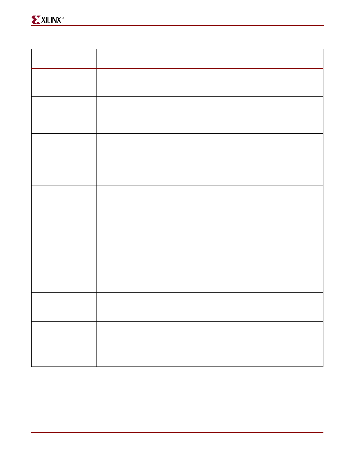
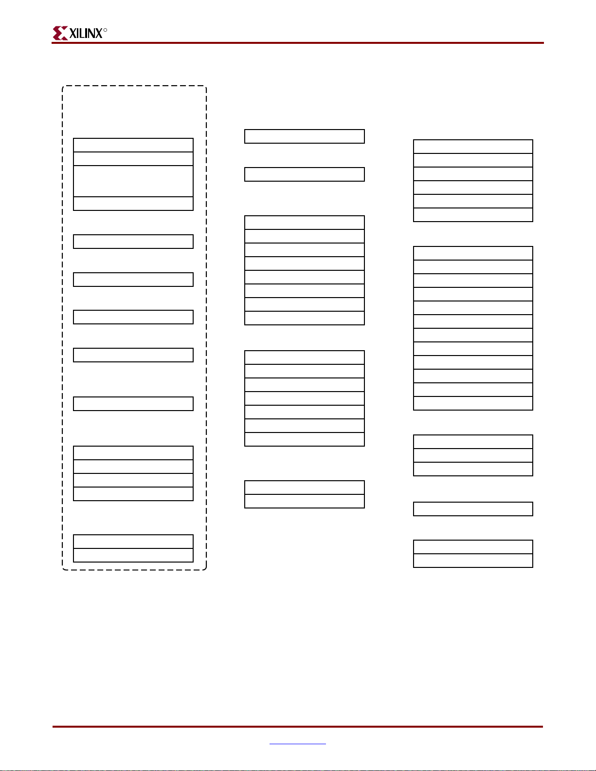
Figure 1-1 shows the registers contained in the PowerPC 405. Descriptions of the registers
are in the following sections.
PowerPC™ 405 Processor Block Reference Guide www.xilinx.com 23
UG018 (v2.0) August 20 , 20 04 1-800-255-7778
Page 24
R
Chapter 1: Introduction to the PowerPC 405 Processor
User Registers
General-Purpose Registers
r0
r1
.
.
.
r31
Condition Register
CR
Fixed-Point Exception Register
XER
Link Register
LR
Count Register
CTR
User-SPR General-Purpose
Registers
USPRG0
SPR General-Purpose
Registers
Time-Base Registers
(read only)
SPRG4
SPRG5
SPRG6
SPRG7
(read only)
TBU
TBL
Privileged Registers
Machine-State Register
MSR
Core-Configuration Register
CCR0
SPR General-Purpose
Registers
SPRG0
SPRG1
SPRG2
SPRG3
SPRG4
SPRG5
SPRG6
SPRG7
Exception-Handling Registers
EVPR
ESR
DEAR
SRR0
SRR1
SRR2
SRR3
Memory-Management
Registers
PID
ZPR
Storage-Attribute Control
Registers
DCCR
DCWR
ICCR
SGR
SLER
SU0R
Debug Registers
DBSR
DBCR0
DBCR1
DAC1
DAC2
DVC1
DVC2
IAC1
IAC2
IAC3
IAC4
ICDBR
Timer Registers
TCR
TSR
PIT
Processor-Version Register
PVR
Time-Base Registers
TBU
TBL
UG018_36_102401
Figure 1-1: PowerPC 4 05 Regist ers
General-Purpose Registers
The processor contains thirty-two 32-bit general-purpose registers (GPRs), identified as r0
through r31. The contents of the GPRs are read from memory using load instructions and
written to memory using store instructions. Computational instructions of ten read
operands from the GPRs and write their results in GPRs. Other instructions move data
between the GPRs and other registers. GPRs can be accessed by all software.
24 www.xilinx.com PowerPC™ 405 Processor Block Reference Gu id e
1-800-255-7778 UG018 (v2.0) August 20, 2004
Page 25

Special-Purpose Registers
The processor contains a number of 32-bit special-purpose registers (SPRs). SPRs provide
access to additional processor resources, such as the count register , the link register , debug
resources, timers, interrupt registers, and others. Most SPRs are accessed only by
privileged software, but a few, such as the count register and link register , are accessed by
all software.
Machine-State Register
The 32-bit machine-state register (MSR) contains fields that control the operating s tate of the
processor. This register can be accessed only by privileged software.
Condition Register
The 32-bit condition register (CR) contains eight 4-bit fields, CR0–CR7. The values in the CR
fields can be used to control conditional branching. Arithmetic instructions can set CR0
and compare instructions can set any CR field. Additional instructions are provided to
perform logical operations and tests on CR fields and bits within the fiel ds. The CR can be
accessed by all software.
R
Device Control Registers
The 32-bit device control registers (not shown) are used to configure, control, and report
status for various external devices that are not part of the PowerPC 405 processor. The
OCM controllers are examples of devices that contain DCRs. Although the DCRs are not
part of the PowerPC 405 implementation, they are accessed using the mtdcr and mfdcr
instructions. The DCRs can be accessed only by privileged software.
PowerPC 405 Hardware Organization
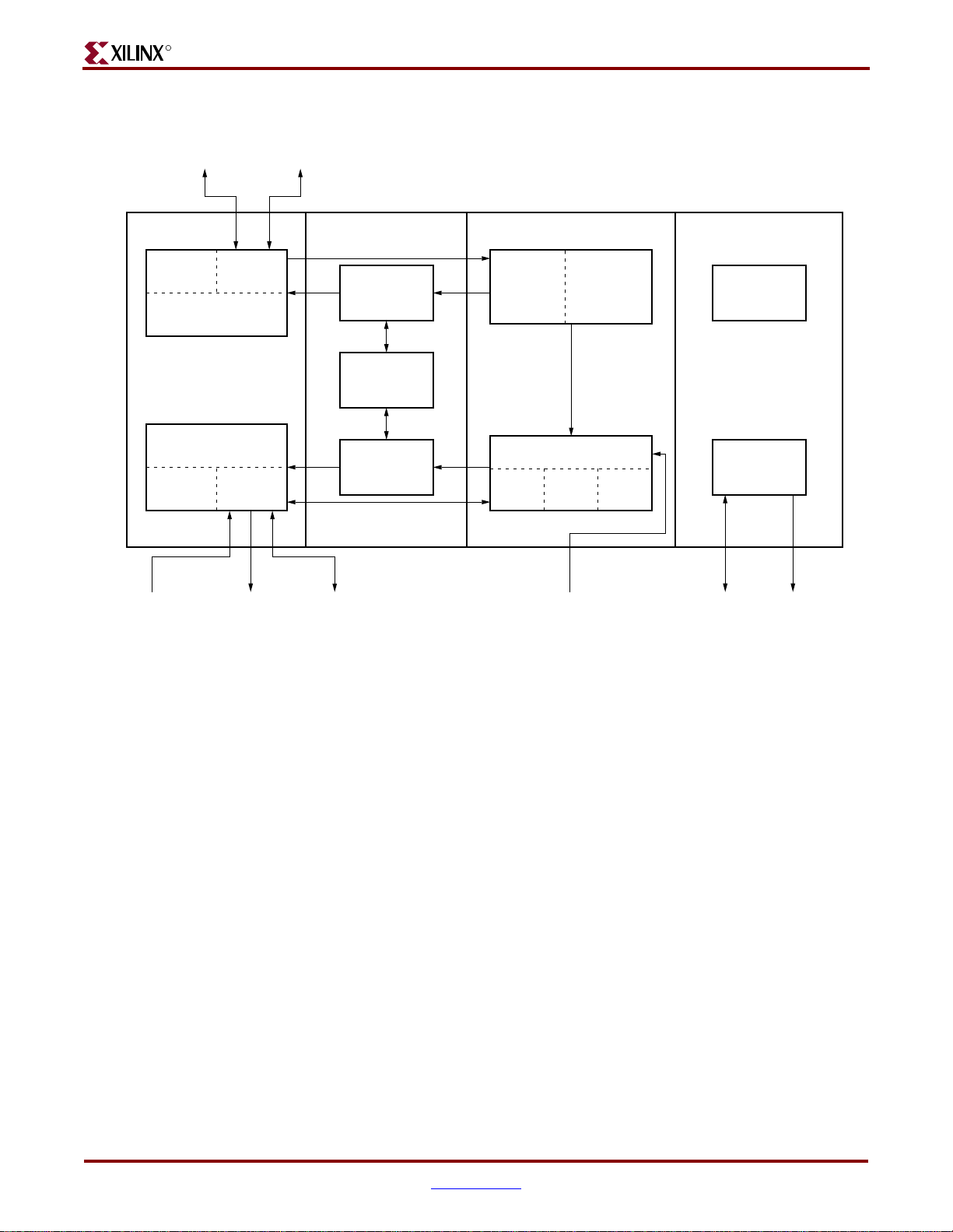
As shown in Figure 1-2, the PowerPC 405 processor contains the following elements:
x A 5-stage pipeline consisting of fetch, decode, execute, write-back, and load write-
back stages
x A virtual-memory-management unit that supports multiple page sizes and a variety
of storage-protection attr ibutes and access-control options
x Separate instruction-cache and data-cache units
x Debug support, including a JTAG interface
x Three programmable timers
The following sections provide an overview of each element. Refer to the PowerPC
Processor Reference Guide for more information on how software interacts with these
elements.
PowerPC™ 405 Processor Block Reference Guide www.xilinx.com 25
UG018 (v2.0) August 20 , 20 04 1-800-255-7778
Page 26
R
Chapter 1: Introduction to the PowerPC 405 Processor
PLB Master
Read Interface
I-Cache
Array
Instruction-Cache
I-Cache
Controller
Unit
Cache Units
Data-Cache
Unit
D-Cache
Array
D-Cache
Controller
Instruction
OCM
Instruction
Shadow-TLB
(4-Entry)
Unified TLB
(64-Entry)
Data
Shadow-TLB
(8-Entry)
Fetch
and
Decode
Logic
32x32
GPR
CPUMMU
3-Element
Fetch Queue
Execute Unit
ALU MAC
Timers
Timers
and
Debug
Debug
Logic
PLB Master
Read Interface
a. Figure 1-2 is specific to PPC405D5.
PLB Master
Write Interface
Central-Processing Unit
The PowerPC 405 central-processing unit (CPU) implements a 5-stage instruction pipeline
consisting of fetch, decode, execute, write-back, and load write-back stages.
The fetch and decode logic sends a steady flow of instructions to the execute unit. All
instructions are decoded before they are forwarded to the execute unit. Instructions are
queued in the fetch queue if execution stalls. The fetch queue consists of three elements:
two prefetch buffers and a decode buffer. If the prefetch buffers are empty instructions
flow directly to the decode buffer.
Up to two branches are processed simultaneo usly by the fetch and decode logic. If a branch
cannot be resolved prior to execution, the fetch and decode logic pr edicts how that branch
is resolved, causing the processor to speculatively fetch instructions from the predicted
path. Branches with negative-address displacements are predicted as taken, as are
branches that do not test the condition register or count register. The default prediction can
be overridden by software at assembly or compile time.
The PowerPC 405 has a single-issue execute unit containing the general-purpose register
file (GPR), arithmetic-logic unit (ALU), and the multiply-accumulate unit (MAC). The
GPRs consist of thirty-two 32-bit registers that are accessed by the execute unit using three
Data
OCM
External-Interrupt
Controller Interface
Figure 1-2: PowerPC 405 Organization
JTAG
a
Instruction
Trace
UG018_35_102401
26 www.xilinx.com PowerPC™ 405 Processor Block Reference Gu id e
1-800-255-7778 UG018 (v2.0) August 20, 2004
Page 27

read ports and two write ports. During the decode stage, data is read out of the GPRs for
use by the execute unit. During the write-back stage, results are written to the GPR. The
use of five read/write ports on the GPRs allows the processor to execute load/store
operations in parallel with ALU and MAC operations.
The execute unit supports all 32-bit PowerPC UISA integer instructions in hardware, and is
compliant with the PowerPC embedded-environment architecture specification. Floatingpoint operations are not supported.
The MAC unit supports implementation-specific multiply-accumulate instructions and
multiply-halfword instructions. MAC instructions operate on either signed or unsigned
16-bit operands, and they store their results in a 32-bit GPR. These instructions can
produce results using either modulo arithmetic or saturating arithmetic. All MAC
instructions have a single cycle throughput.
Exception Handling Logic
Exceptions are divided into two classes: critical and noncritical. The PowerPC 405 CPU
services exceptions caused by error conditions, the internal timers, debug events, and the
external interrupt controller (EIC) interface. Across the two classes, a total of 19 possible
exceptions are supported, including the two provided by the EIC interface.
R
Each exception class has its own pair of save/restore registers. SRR0 and SRR1 are used for
noncritical interrupts, and SRR2 and SRR3 are used for critical interrupts. The exceptionreturn address and the machine state are written to these registers when an exception
occurs, and they are automatically restored when an interrupt handler exits using the
return-from-interrupt (rfi) or r et urn- from critical-interrupt (rfci) instruction. Use of
separate save/restore registers allows the PowerPC 405 to handle critical interrupts
independently of noncritical interrupts.
Memory Management Unit
The PowerPC 405 supports 4 GB of flat (non-segmented) address space. The memorymanagement unit (MMU) provides address translation, protection functions, and storageattribute control for this address space. The MMU supports demand-paged virtual
memory using multiple page sizes of 1 KB, 4 KB, 16 KB, 64 KB, 256 KB, 1 MB, 4 MB and
16 MB. Multiple page sizes can improve memory efficiency and minimize the number of
TLB misses. When supported by system software, the MMU provides the following
functions:
x Translation of the 4 GB logical-address spac e into a physical-address space.
x Independent enabling of instruction translati on and protection from that of data
translation and pro tect io n .
x Page-level access control using the translation m e chanism.
x Software control over the page-replacement strategy.
x Additional protection control using zones.
x Storage attributes for cache policy and speculative memory-access control.
The translation look-aside buffer (TLB) is used to control memory translation and
protecti on. Each o ne of i ts 6 4 en trie s s peci fie s a page translation. It is fully associative, and
can simultaneously hold translations for any combination of page sizes. To prevent TLB
contention between data and instruction accesses, a 4-entry instruction and an 8-entry data
shadow-TLB are maintained by the processor transparently to software.
PowerPC™ 405 Processor Block Reference Guide www.xilinx.com 27
UG018 (v2.0) August 20 , 20 04 1-800-255-7778
Page 28

R
Software manages the initialization and replacement of TL B entries. The PowerPC 405
includes instructions for managing TLB entries by software running in privileged mode.
This capability gives significant control to system software over the implementation of a
page replacement strategy. For example, software can reduce the potential for TLB
thrashing or delays associated with TLB-entry replacement by reserving a subset of TLB
entries for globally accessible pages or critical pages.
Storage attributes are provided to control access of memory regions. When memory
translation is enabled, storage attributes are maintained on a page basis and read from the
TLB when a memory access occurs. When memory translation is disabled, storage
attributes are maintained in storage-attribute control registers. A zone-protection register
(ZPR) is provided to allow system software to override the TLB access controls without
requiring the manipulation of individual TLB entries. For example, the ZPR can provide a
simple method for denying read access to certain application programs.
Instruction and Data Caches
The PowerPC 405 accesses memory through the instruction-cache unit (ICU) and datacache unit (DCU). Each cache unit includes a PLB-master interface, cache arrays, and a
cache controller . Hits into the instruction cache and data cache appear to the CPU as singlecycle memory accesses. Cache misses are h andled as requests over the PLB bus to another
PLB device, such as an external-memory controller.
Chapter 1: Introduction to the PowerPC 405 Processor
The PowerPC 405 implements separate instruction-cache and data-cache arrays. Each is 16
KB in size, is two-way set-associative, and operates using 8 word (32 byte) cache lines. Th e
caches are non-blocking, allowing the PowerPC 405 to overlap instruction execution with
reads over the PLB (when cache misses occur).
The cache controllers replace cache lines according to a least-recently used (LRU)
replacement policy. When a cache line fill occurs, the most-recently accessed line in the
cache set is retained and the other line is replaced. The cache controller updates the LRU
during a cache line fill.
The ICU supplies up to two instructions every cycle to the fetch and decode unit. The ICU
can also forward instructions to the fetch and decode unit during a cache line fill,
minimizing execution stalls caused by instruction-cache misses. When the ICU is accessed,
four instructions are read from the appropriate cache line and placed temporarily in a line
buffer . Subsequent ICU accesses check this line buf fer for the requested instruction prior to
accessing the cache array. This allows the ICU cache array to be accessed as little as once
every four instructions, significantly reducing ICU power cons umption.
The DCU can independently process load/store operations and cache-control instructions.
The DCU can also dynamically reprioritize PLB requests to reduce the length of an
execution stall. For example, if the DCU is busy with a low-priority request and a
subsequent storage operation requested by the CPU is stalled, the DCU automatically
increases the priority of the current (low-priority) request. The current request is thus
finished sooner, allowing the DCU to process the stalled request sooner. The DCU can
forward data to the execute unit during a cache line fill, further minimizing execution stalls
caused by data-cache misses.
Additional features allow programmers to tailor data-cache performanc e to a specific
application. The DCU can function in write-back or write-through mode, as determined by
the storage-control attributes. Loads and stor es that d o not allocate cache lines can also be
specified. Inhibiting certain cache line fills can reduce potential pipeline sta lls and
unwanted external-bus traffic.
28 www.xilinx.com PowerPC™ 405 Processor Block Reference Gu id e
1-800-255-7778 UG018 (v2.0) August 20, 2004
Page 29

Timer Resources
The PowerPC 405 contains a 64-bit time base and three timers. The time base is
incremented synchronously using the CPU clock or an external clock source. The three
timers are incremented synchronously with the time base. The three timers supported by
the PowerPC 405 are:
x Programmable Interval Timer
x Fixed Interval Timer
x Watch dog Timer
Programmable Interval Timer
The pr ogrammable interval timer (PIT) is a 32-bit register that is decremented at the time-base
increment frequency. The PIT register is loaded with a delay value. When the PIT count
reaches 0, a PIT interrupt occurs. Optionally , the PIT can be programmed to automatically
reload the last delay value and begin decrementing again.
Fixed Interval Timer
The fixed interval timer (FIT) causes an interrupt when a selected bit in the time-base register
changes from 0 to 1. Programmers can select one of four predefined bits in the time-base
for triggering a FIT interrupt.
R
Debug
Watchdog Timer
The watchdog timer causes a hardware reset when a selected bit in the time-base register
changes from 0 to 1. Programmers can select one of four predefined bits in the time-base
for triggering a reset, and the type of reset can be defined by the programmer.
The PowerPC 405 debug resources include special debug modes that support the various
types of debugging used during hardware and software development. These are:
x Internal-debug mode for use by ROM monitors and software debuggers
x External-debug mode for use by JTAG debuggers
x Debug-wait mode, which allows the servicing of interrupts while the processor appears
to be stopped
x Real-time trace mode, which supports event triggering for real-time tracing
Debug events are supported that allow developers to manage the debug process. Debug
modes and debug events are controlled using debug registers in the processor. The debug
registers are accessed either through software running on the processor or through the
JTAG port.
The debug modes, events, controls, and interfaces provide a powerful combination of
debug resour ces f or hardw are and software development tools.
PowerPC 405 Interfaces
The PowerPC 405 provides the following set of interfaces that support the attachment of
cores and user logic:
x Processor local bus interface
PowerPC™ 405 Processor Block Reference Guide www.xilinx.com 29
UG018 (v2.0) August 20 , 20 04 1-800-255-7778
Page 30

R
x Device control register interface
x Clock and power management interface
x JTAG port interface
x On-chip interrupt controller interface
x On-chip memory controller interface
Processor Local Bus
The processor local bus (PLB) i nterface provides a 32-bit address and three 64-bit data buses
attached to the instruction-cache and data-cache units. T wo of the 64-bit buses are attached
to the data-cache unit, one supporting read operations and the other supportin g write
operations. The third 64-bit bus is attached to the instruction-cache unit to support
instruction fetching.
Device Control Register
The device control register (DC R) bus interface supports the attachment of on-chip registers
for device control. Software can access these registers using the mfdcr and mtdcr
instructions.
Chapter 1: Introduction to the PowerPC 405 Processor
Clock and Power Management
The clock and power-management interface supports several methods of clock distribution
and power management.
JTAG Port
The JTAG port interface supports the att achment of external debug tools. Using the JTAG
test-access port, a debug tool can single-step the processor and examine internal-processor
state to facilitate software debugging.
On-Chip Interrupt Controller
The on-chip interrupt controller interface is an external interrupt controller that combines
asynchronous interrupt inputs from on-chip and off-chip sources and presents them to the
core using a pair of interrupt signals (critical and noncritical). Asynchronous interrupt
sources can include external signals, the JTAG and debug units, and any other on-chip
peripherals.
On-Chip Memory Controller
An on-chip memory (OCM) interface supports the attachment of additional memory to the
instruction and data caches that can be accessed at performance levels matching the cache
arrays.
PowerPC 405 Performance
The PowerPC 405 executes instructions at sustained speeds approaching one cycle per
instruction. Table 1-3 lists the typical execution speed (in processor cycles) of the
instruction classes supported by the PowerPC 405.
Instructions that access memory (loads and stores) consider only the “first order” effects of
cache misses. The performance penalty associated with a cache miss involves a number of
second-order effects. This includes PLB contention between the instruction and data
30 www.xilinx.com PowerPC™ 405 Processor Block Reference Gu id e
1-800-255-7778 UG018 (v2.0) August 20, 2004
Page 31

caches and the time associated with perf orming cache-line fills and flushes. Unless stated
otherwise, the number of cycles described applies to systems having zero-wait-state
memory access.
Table 1-3: PowerPC 405 Cycles per Instruction
Instruction Class Execution Cycles
Arithmetic 1
Trap 2
Logical 1
Shift and Rotate 1
Multiply (32-bit, 48-bit, 64-bit results, respectively) 1, 2, 4
Multiply Accumulate 1
Divide 35
R
Load 1
Load Multiple and Load String (cache hit) 1 per data transfer
Store 1
Store Multiple and Store String (cache hit or miss) 1 per data transfer
Move to/from device-control register 3
Move to/from special-purpose register 1
Branch known taken 1 or 2
Branch known not taken 1
Predicted taken branch 1 or 2
Predicted not-taken branch 1
Mispredicted branch 2 or 3
PowerPC™ 405 Processor Block Reference Guide www.xilinx.com 31
UG018 (v2.0) August 20 , 20 04 1-800-255-7778
Page 32

R
Chapter 1: Introduction to the PowerPC 405 Processor
32 www.xilinx.com PowerPC™ 405 Processor Block Reference Gu id e
1-800-255-7778 UG018 (v2.0) August 20, 2004
Page 33

R
Input/Output Interfaces
This chapter describes all PowerPC 405 input/output signals associated with the following
processor block interfaces:
x “Clock and Power Management Interface”
x “CPU Control Interfa ce”
x “Reset Interface”
x “Instruction-Side Processor Local Bus Interface”
x “Data-Side Processor Local Bus Interface”
x “Device-Control Register Interfaces”
x “Internal Dev ice Control Register (DCR) Interface”
x “External DCR Bus Interface”
x “External In t e rrupt Controller Inter f ace”
x “PPC405 JTAG Debug Port”
x “Debug Interface”
x “Trace Interface”
x “Processor Version Register (PVR) Interface (Virtex-4-FX Only)”
x “Additional FPGA Specif ic Signals”
Chapter 2
The sections within this chapter provide the following in f ormation:
x An overview summarizing the purpose of the interface.
x An I/O symbol providing a quick view of the signal names and the direction of
information flow with respect to the processor block.
x A signal table that summarizes the function of each signal. The I/O column in these
tables specifies the direction of information flow with respect to the processor block.
x Detailed descriptions for each signal.
x Detailed timing diagrams (where appropriate) that more clearly describe the
operation of the interface. The diagrams typically illustrate best-case performance
when the core is attached to the FPGA processor local bus (PLB) core, or to custom
bus interface unit (BIU) desig ns.
The instruction-side and data-side OCM controller interfaces are described separately in
Chapter 3, “PowerPC 405 OCM Controller.”
The Fabric Co-Processor Module (FCM) interface associated with the Virtex-4-FX family
PowerPC 405 APU controller, is described separately in Chapter 4, “PowerPC 405 APU
Controller.”
PowerPC™ 405 Processor Block Reference Guide www.xilinx.com 33
UG018 (v2.0) August 20 , 20 04 1-800-255-7778
Page 34

R
Appendix B, “Signal Summary,” alphabetically lists the signals described in this chapter.
The l/O designation and a descri ption summary are included for each signal.
Signal Naming Conventions
The following convention is used fo r signal names throughout this document:
PREFIX1PREFIX2SIGNAME1[SIGNAME2][NEG][(m:n)]
The components of a signal name are as follows:
x PREFIX1 is an uppercase prefix identifying the source of the signal. This prefix
specifies either a unit (for example, CPU) or a type of interface (for example, DCR). If
PREFIX1 specifies the processor block, the signal is considered an output signal.
Otherwise, it is an input signal.
x PREFIX2 is an uppercase prefix identifying the destination of the signal. This prefix
specifies either a unit (for example, CPU) or a type of interface (for example, DCR). If
PREFIX2 specifies the processor block, the signal is considered an input signal.
Otherwise, it is an output signal.
x SIGNAME1 is an uppercase name identifying the primary function of the signal.
x SIGNAME2 is an uppercase name identifying the secondary function of the signal.
x [NEG] is an optional notation that indicates a signal is active low. If this notation is not
use, the signal is active high.
x [m:n] is an optional notation that indicates a bussed signal. “m” d esignates the most-
significant bit of the bus and “n” designates the least-s ignificant bit of the bus.
Chapter 2: Input/Output Interfaces
Table 2-1 defines the prefixes used in the signal names. The “Location” column in the table
identifies whether the functional unit resides inside or outside the processor block.
Table 2-1: Signal Name Prefix Definitions
Prefix1 or Prefix2 Definition Location
CPM Clock and power management Outside
C405 Processor block Inside
DBG Debug unit Inside
DCR Device control register Outside
DSOCM Data-side on-chip memory (DSOCM) Outside
a
EIC External interrupt controller Outside
ISOCM Instruction-side on-chip memory (ISOCM) Outside
a
JTG JTAG Inside
PLB Processor local bus Inside
RST Reset Inside
TIE TIE (signal tied statically to GND or V
)Outside
DD
TRC Trace Inside
APU Auxiliary Processor Unit Controller Inside
FCM Fabric Co-Processor Module Outside
34 www.xilinx.com PowerPC™ 405 Processor Block Reference Gu id e
1-800-255-7778 UG018 (v2.0) August 20, 2004
Page 35

Table 2-1: Signal Name Prefix Definitions (Continued)
Prefix1 or Prefix2 Definition Location
BRAM BlockSelect RAM Outside
XXX Unspecified FPGA unit Outside
a. Not to be confused with the OC M controllers, which are located inside the processor block.
Clock and Power Management Interface
The clock and power management (CPM) interf ace enables power-sensitive applications
to control the processor clock using external logic. The OCM controllers are clocked
separately from the processor core. In addition to this, the Virtex-4-FX family PowerPC 405
also use separate clocks for the APU and DCR controller. Two types of processor clock
control are possible:
x Global local enables control a clock zone within the processor. These signals are used to
disable the clock splitters within a zone so that the clock signal is prevented from
propagating to the latches within the zone. The PowerPC 405 is divided into three
clock zones: core, timer, and JTAG. Control over a zone is exercised as follows:
i The core clock zone contains most of the logic comprising the PowerPC 405 core
and controllers. It does not contain logic that belongs to the timer or JTAG zones,
or other logic within the processor block. The core zone is controlled by the
CPMC405CPUCLKEN signal.
i The timer clock zone contains the PowerPC 405 timer logic. It does not contain
logic that belongs to the core or JTAG zones, or other logic within the processor
block. This zone is separated from the core zone so that timer events can be used
to “wake up” the core logic if a power management application has put it to sleep.
The timer zone is controlled by the CPMC405TIMERCLKEN signal.
i The JTAG clock zone contains the PowerPC 405 JTAG logic. It does not contain
logic that belongs to the core or timer zones, or other logic w ithin the processor
block. The JTAG zone is controlled by the CPMC405JTAGCLKEN signal.
Although an enable is provided for this zone, the JTAG standard does not allow
local gating of the JTAG clock. This enables basic J TAG functions to be m aint aine d
when the rest of the chip (including the CPM FPGA macro) is not running.
x Global gating controls the toggling of the PowerPC 405 clock, CPMC405CLOCK.
Instead of using the global-local enables to prevent the clock signal from propagating
through a zone, CPM logic can stop the PowerPC 405 clock input from toggling. If this
method of power management is employed, the clock signal should be held active
(logic 1). The CPMC405CLOCK is used by the core and timer zones, but not the JTAG
zone.
R
CPM logic should be designed to wake the PowerPC 405 from sleep mode when any of the
following occurs:
i A timer interrupt or timer reset is asserted by the PowerPC 405.
i A chip-reset or system-reset request is asserted (this request comes from a source
other than the PowerPC 405).
i An external interrupt or critical interrupt input is asserted and the corresponding
interrupt is enabled by the appropriate machine-state register (MSR) bit.
PowerPC™ 405 Processor Block Reference Guide www.xilinx.com 35
UG018 (v2.0) August 20 , 20 04 1-800-255-7778
Page 36

R
i The DBGC405DEBUGHALT chip-input signal (if provided) is asserted. Assertion
of this signal indicates that an external debug tool w ants to control the PowerPC
405 processor. See “DBGC405DEBUGHALT (Input)” for more information.
CPM Interface I/O Signal Summary
Figure 2-1 shows the block symbol for the CPM interface. The BRAM clocks associated
with the data-side and instruction-side OCM are described in chapter Chapter 3,
“PowerPC 405 OCM Controller.” The signals are summarized in Table 2-2.
Chapter 2: Input/Output Interfaces
CPMC405CLOCK
PLBCLK
CPMC405CPUCLKEN
CPMC405TIMERCLKEN
CPMC405JTAGCLKEN
CPMC405CORECLKINACTIVE
CPMC405TIMERTICK
CPMC405SYNCBYPASS
CPMDCRCLK
CPMFCMCLK
PPC405
C405CPMMSREE
C405CPMMSRCE
C405CPMTIMERIRQ
C405CPMTIMERRESETREQ
C405CPMCORESLEEPREQ
UG018_02_01_051204
Figure 2-1: CPM Interface Block Symbol
Table 2-2: CPM Interface I/O Signals
Signal
I/O
Type
If Unused Function
CPMC405CLOCK I Required PowerPC 405 clock input (for all non-JT AG logic,
including timers).
PLBCLK I Required PLB clock interface clock ( la c ks CPM prefix due
to legacy naming).
CPMC405CPUCLKEN I 1 Enables the core clock zone.
CPMC405TIMERCLKEN I 1 Enables the timer clock zone.
CPMC405JTAGCLKEN I 1 Enables the JTAG clock zone.
CPMC405CORECLKINACTIVE I 0 Indicates the CPM logic disabled the clocks to the
core.
CPMC405TIMERTICK I 1 Increments or decrements the PowerPC 405
timers every time it is active with the
CPMC405CLOCK.
CPMC405SYNCBYPASS I 1 Virtex-4-FX only. Bypass PLB re-synchronization
inside the PowerPC 405 core for Virtex-II Pro
compatibility.
CPMDCRCLK I 0 Virtex-4-FX only. DCR bus interface clock for
PPC405 synchr on ization.
CPMFCMCLK I 0 Virtex-4-FX only. FCM interface clock for the
APU Controller.
36 www.xilinx.com PowerPC™ 405 Processor Block Reference Gu id e
1-800-255-7778 UG018 (v2.0) August 20, 2004
Page 37

Table 2-2: CPM Interface I/O Signals (Continued)
R
Signal
C405CPMMSREE O No Connect Indicates the value of MSR[EE].
C405CPMMSRCE O No Connect Indicates the value of MSR[CE].
C405CPMTIMERIRQ O No Connect Indicates a timer-interrupt request occurred.
C405CPMTIMERRESETREQ O No Connect Indicates a watchdog-timer reset request
C405CPMCORESLEEPREQ O No Connect Indicates the core is requesting to be put into
I/O
Type
If Unused Function
occurred.
sleep mode.
CPM Interface I/O Signal Descriptions
The following sections describe the operation of the CPM interface I/O signals.
CPMC405CLOCK (Input)
This signal is the source clock for all PowerPC 405 logic (including timers). It is not the
source clock for the JTA G logic. External logic can implement a power management mode
that stops toggling of this signal. If such a method is employed, the clock signal should be
held active (logic 1).
PLBCLK (Input)
This signal is the source clock for all PLB logic.
CPMC405CPUCLKEN (Input)
Enables the core clock zone when asserted and disables the zone when deasserted. If logic
is not implemented to control this signal, it must be held active (tied to 1).
CPMC405TIMERCLKEN (Input)
Enables the timer clock zone when asserted and disables the zone when deasserted. If logic
is not implemented to control this signal, it must be held active (tied to 1).
CPMC405JTAGCLKEN (Input)
Enables the JTAG clock zone when asserted and disables the zone when deasserted. CPM
logic should not control this signal. The JTAG standard requires that it be held active (tied
to 1).
CPMC405CORECLKINACTIVE (Input)
This signal is a status indicator that is latched by an internal PowerPC 405 register (JDSR).
An external debug tool (such as RISCWatch) can read this register and determine that the
PowerPC 405 is in sleep mode. This signal should be asserted by the CPM when it places
the PowerPC 405 in sleep mode using either of the following methods:
x Deasserting CPMC405CPUCLKEN to disable the core clock zone.
x Stopping CPMC405CLOCK from toggling by holding it active (logic 1).
PowerPC™ 405 Processor Block Reference Guide www.xilinx.com 37
UG018 (v2.0) August 20 , 20 04 1-800-255-7778
Page 38

R
CPMC405TIMERTICK (Input)
This signal is used to control the update frequency of the PowerPC 405 time base and PIT
(the FIT and WDT are timer events triggered by the time base). The time base is
incremented and the PIT is decremented every cycle that CPMC405TIMERTICK and
CPMC405CLOCK are both active. CPMC405TIMERTICK should be synchronous with
CPMC405CLOCK for the timers to operate predictably. The timers are updated at the
PowerPC 405 clock frequency if CPMC405TIMERTICK is held active.
CPMC405SYNCBYPASS (Input, Virtex-4-FX Only)
Allows the user to bypass the PLB synchronization module inside the PowerPC core and
instead use a Virtex-II Pro compatible synchronizer in the processor block. When this
signal is enabled, integer clock ratios between 1:1 and 16:1 are possible. If disabled, the user
can use fractional clock ratios of N/2 and N/3 for any in tege r N, but must also ensure that
PLB and CPU clocks are rising-edge aligned, and accept additional latency for the
synchronization.
CPMDCRCLK (Input, Virtex-4-FX Only)
This is the DCR interface clock used by the PPC to synchronize communication between
the PowerPC’s internal clock domain (CPMC405CLOCK) and the DCR bus transactions
performed using the DCR slave clocks. The PowerPC core to DCR interface clock ratio can
be any integer between 1:1 and 16:1. Clocks must be rising-edge aligned.
Chapter 2: Input/Output Interfaces
CPMFCMCLK (Input, Virtex-4-FX Only)
This is the re-synchronization clock for transactions between the APU controller and an
FCM. Allows the APU controller internally to run at the CPMC405CLOCK speed ,
independently of the FCM interface transactio n speed. CPMFCMCLK would typically be
the same clock that clocks the FCM internally. PowerPC core to FCM interface clock ratio
can be any integer between 1:1 and 16:1. Clocks must be rising-edge aligned.
C405CPMMSREE (Output)
This signal indicates the state of the MSR[EE] (external-interrupt enable) bit. When
asserted, external interrupts are enabled (MSR[EE]=1). When deasserted, external
interrupts are disabled (MSR[EE]=0). The CPM can use this signal to wake the processor
from sleep mode when an external noncritical interrupt occurs.
When the processor wakes up, it deasserts the C405CPMMSREE, C405CPMMSRCE, and
C405CPMTIMERIRQ signals one processor clock cycle before it deasserts the
C405CPMCORESLEEPREQ signal. Consequently, the CPM should latch the
C405CPMMSREE, C405CPMMSRCE, and C405CPMTIMERIRQ signals before using them
to control the processor clocks.
C405CPMMSRCE (Output)
This signal indicates the state of the MSR[CE] (critical-interrupt enable) bit. When asserted,
critical interrupts are enabled (MSR[CE]=1). When deasserted, critical interrupts are
disabled (MSR[CE]=0). The CPM can use this signal to wake the processor from sleep
mode when an external critical interrupt occurs.
When the processor wakes up, it deasserts the C405CPMMSREE, C405CPMMSRCE, and
C405CPMTIMERIRQ signals one processor clock cycle before it deasserts the
C405CPMCORESLEEPREQ sign al. For this reason, the CPM should latch the
38 www.xilinx.com PowerPC™ 405 Processor Block Reference Gu id e
1-800-255-7778 UG018 (v2.0) August 20, 2004
Page 39

C405CPMMSREE, C405CPMMSRCE, and C405CPMTIMERIRQ signals before using them
to control the processor clocks.
C405CPMTIMERIRQ (Output)
When asserted, this signal indicates a timer exception occurred within the PowerPC 405
and an interrupt request is pending to handle the exception. When deasserted, no timerinterrupt request is pending. This signal is the logical OR of interrupt requests from the
programmable-interval t imer (PIT), the fixed-inte rval timer (FIT), and the wat chdog timer
(WDT). The CPM can use this signal to wake the processor from sleep mode when an
internal timer exception occurs.
When the processor wakes up, it deasserts the C405CPMMSREE, C405CPMMSRCE, and
C405CPMTIMERIRQ signals one processor clock cycle before it deasserts the
C405CPMCORESLEEPREQ signal. Consequently, the CPM should latch the
C405CPMMSREE, C405CPMMSRCE, and C405CPMTIMERIRQ signals before using them
to control the processor clocks.
C405CPMTIMERRESETREQ (Output)
When asserted, this signal indicates a watchdog time-out occurred and a reset request is
pending. When deasserted, no reset request is pending. This signal is the logical OR of the
core, chip, and system reset modes that are programmed using the watchdog timer
mechanism. The CPM can use this signal to wake the processor from sleep mode when a
watchdog time-out occurs.
R
C405CPMCORESLEEPREQ (Output)
When asserted, this signal indicates the PowerPC 405 has requested to be put into sleep
mode. When deasserted, no request exists. This signal is asserted after software enables the
wait state by setting the MSR[WE] (wait-state enable) bit to 1. The processor completes
execution of all prior instructions and memory accesses before asserting this signal. The
CPM can use this signal to place the processor in sleep mode at the request of software.
When the processor gets out of sleep mode at a later time, it deasserts the
C405CPMMSREE, C405CPMMSRCE, and C405CPMTIMERIRQ signals o ne processo r
clock cycle before it deasserts the C405CPMCORESLEEPREQ signal. Consequently, the
CPM should latch the C405CPMMSREE, C405CPMMSRCE, and C405CPMTIMERIRQ
signals before using them to control the processor clocks.
System Design Considerations for Clock Domains
The high-level view of an embedded system with the PowerPC 405 processor and
CoreConnect bus architecture includes:
x PowerPC 405 Processor.
x Processor Local Bus (PLB) peripherals.
x Instruction-side and Data-side On-Chip Memory Controller (OCM).
x Device Control Register (DCR) peripherals.
x Fabric Co-Processor Module (FCM): Virtex-4 only.
These clocks communicate to the processor block the specific clock ratio between the
processor block clock and the other system clocks in the design.
x CPMC405CLOCK, main Processor Block clock.
PowerPC™ 405 Processor Block Reference Guide www.xilinx.com 39
UG018 (v2.0) August 20 , 20 04 1-800-255-7778
Page 40

R
x PLBCLK, primary PLB I/O Bus clock.
x BRAMISOCMCLK, reference clock for the I-Side OCM controller.
x BRAMDSOCMCLK, reference clock for the D-Side OCM controller.
x CPMFCMCLK, reference clock for the APU controller (Virtex-4 only).
x CPMDCRCLK, reference clock for the external DCR bus (Virtex-4 only).
The PowerPC405 processor block supports multiple clock domains. Using several DCM
and BUFG components ar e recommended to cr eate and drive the clock domains. The cl ock
domains include the PLB, FCM, DCR, and OCM clocks.
Chapter 2: Input/Output Interfaces
PLB
The PLB is used as an interface between the processor block and the higher performance
peripherals. The processor block has some internal logic to generate the appropriate
enabling signals for controlling the PLB . The PLB clock must be phased-aligned to the
processor block. All communication between the processor block and the PLB are based
upon the rising edge of the CPMC405CLOCK. The PLB is synchronous with the processor
block. The allowed supported integer clock frequency ratios between the processor block
and the PLB are 1:1, 2:1, 3:1 . . . up to 16:1. As an example, the processor block can be run at
300 MHz whil e t he PLB bus is run at 100 MHz, in a 3:1 r at io.
DCR
The processor block clock and the DCR clock must come from the same source and be in
phase with each other. The DCR clock covers both of the processor block DCR and the
memory mapped DCR. The clock ratio between the DCR clock domain and the processor
block can run at any integer clock ratio from 1:1 to 16:1 as lon g as the bus transaction
completes in 64 processor block cycles. If the bus transaction does not complete in 64
processor block clock cycles, the processor block will time out and move on to the next
instruction.
Virtex-II Pro and ProX Specific
For Virtex-II Pro and Virtex-II ProX devices, there is no CPMDCRCLK input to the
processor block. Users can either set appropriate timing constraints (multi-cycle path, false
path, etc.), or simply include DCR re-synchronization logic to simply the steps to analyze
the timing related to DCR interface.
Virtex-4 Specific
For Virtex-4-FX parts there is a dedicated DCR clock input and re-synchronization registers
handling the clock boundary.
FCM (Virtex-4-FX only)
An FCM is used for highest performance integration of custom functionality defined in the
FPGA fabric with the execution pipeline of the PowerPC. Th e F C M clock would typically
be the same clock that clocks the FCM internally. PowerPC core to FCM interface clock
ratios can range from 1:1 to 16:1. The clocks must be rising-edge aligned.
OCM
For high speed access, the OCM clock domain covers the interface between the processor
block and the block RAM surrounding the processor block. There are two independent
40 www.xilinx.com PowerPC™ 405 Processor Block Reference Gu id e
1-800-255-7778 UG018 (v2.0) August 20, 2004
Page 41

clocks for the OCM controllers in the processor block: BRAMDSOCMCLK (data side
controller) and BRAMISOCMCLK (instruction side controllers).
The data side controller and the instruction side controllers can run at different
frequencies, based upon the access time of the BRAM. When the processor block, OCM
controller, and BRAMs run at the same clock frequency, the processor is in single-cycle
mode. Multi-cycle mode occurs when the processor is running at a higher frequency than
the BRAMs. In the single-cycle mode and multi-cycle mode, the BRAMISOCMCLK and
BRAMDSOCMCLK signals are provided to the OCM controller as inputs.
Through timing analysis, the clock ratio between the processor block clock and the BRAMs
clocks is determined by the worst case access time between the OCM controller interface
and the BRAMs interface. Based upon the timing analysis, most designs use multi-cycle
mode.
The processor block clock and the BRAMDSOCMCLK must be integer multiples. The
same is true for the BRAMISOCMCLK with r espect to the processor block clock. They need
not share the same integer values nor integer clock ratio with respect to the PLB clock.
Because the clock ratio between the processor block and the OCM clocks is unknown, the
processor block has control registers in the OCM controllers. The control registers are
ISCNTL[0:7] and DSCNTL[0:7] for the instruction side an d data side, r espectively. Refer to
Chapter 3, “PowerPC 405 OCM Controller” for more details.
R
CPU Control Interface
The CPU control interface is used primarily to provide CPU setup information to the
PowerPC 405. It is also used to report the detection of a machine check condition within the
PowerPC 405.
CPU Control Interface I/O Signal Summary
Figure 2-2 shows the block symbol for the CPU control interface. The signals are
summarized in Table 2-3.
TIEC405MMUEN
TIEC405DETERMINISTICMULT
TIEC405DISOPERANDFWD
Figure 2-2: CPU Control Interface Block Symbol
Table 2-3: CPU Control Interface I/O Signals
Signal
I/O
Type
If Unused Function
TIEC405MMUEN I Required Enables the memory-management unit (MMU).
PPC405
C405XXXMACHINECHECK
UG018_02_102001
TIEC405DETERMINISTICMULT I 0
Important: This signal should always be driven low.
Specifies whether all multiply operations complete in
a fixed number of cycles or have an early-out
capability
PowerPC™ 405 Processor Block Reference Guide www.xilinx.com 41
UG018 (v2.0) August 20 , 20 04 1-800-255-7778
Page 42

R
Table 2-3: CPU Control Interface I/O Signals (Continued)
Chapter 2: Input/Output Interfaces
Signal
I/O
Type
If Unused Function
TIEC405DISOPERANDFWD I Required Disables operand forwa rding for load instructions.
C405XXXMACHINECHECK O No Connect Indicates a machine-check error has been detected by
the PowerPC 405.
CPU Control Interface I/O Signal Descriptions
The following sections describe the operation of the CPU control-interface I/O signals.
TIEC405MMUEN (Input)
When held active (tied to logic 1), this signal enables the PowerPC 405 memorymanagement unit (MMU). When held inactive (tied to logic 0), this signal disables the
MMU. The MMU is used for virtual to address translation and for memory protection. Its
operation is described in the PowerPC Processor Reference Guide.
TIEC405DETERMINISTICMULT (Input)
Note: This signal should always be driven low. Setting it high may produce erroneous results.
When held active (tied to logic 1), this sign al d isables the hardware multiplier early-out
capability. All multiply instructions have a 4-cycle reissue rate and a 5-cycle latency rate.
When held inactive (tied to logic 0), this signal enables the hardware multiplier early-out
capability. If early out is enabled, multiply instructions are executed in the number of
cycles specified in Table 2-4. The performance of multiply instructions is described in the
PowerPC Processor Reference Gu ide.
Table 2-4: Multiply and MAC Instruction Timing
Operations
Issue-Rate
Cycles
MAC and Negative MAC 1 2
Halfword
Halfword
Word
uHalfword (32-bit result) 1 2
uWord (48-bit re sult) 2 3
uWord (64-bit result) 4 5
Note: In Table 2-4, above, words are trea ted as halfwords if the upper 16 bits of the ope rand contain
a sign extension of the lowe r 16 bits. For example, i f the upper 1 6 bits of a word oper and are zero, the
operand is considered a halfword when calculating the execution time.
TIEC405DISOPERANDFWD (Input)
When held active (tied to logic 1), this signal disables operand forwarding. When held
inactive (tied to logic 0), this signa l enables operand forwarding. The processor uses
operand forwarding to send load-instruction data from the data cache to the execution
units as soon as it is availabl e. Operand forwarding often saves a clock cycle when
Latency
Cycles
42 www.xilinx.com PowerPC™ 405 Processor Block Reference Gu id e
1-800-255-7778 UG018 (v2.0) August 20, 2004
Page 43

C405XXXMACHINECHECK (Output)
Reset Interface
R
instructions following the load require the loaded data. Disabli ng operand forwarding
may improve the performance (clock frequency) of the PowerPC 405.
When asserted, this signal indicates the PowerPC 405 detected an instruction machinecheck error. When deasserted, no error exists. This signal is asserted when the processor
attempts to execute an instruction that was transferred to the PowerPC 405 with the
PLBC405ICUERR signal asserted. This signal remains as serted until software clears the
instruction machine-check bit in the exception-syndrome register (ESR[MCI]).
A reset causes the processor block to perform a hardware initialization. It always occurs
when the processor block is powered up and can occur at any time during normal
operation. If it occurs during normal operation , instruction execution is immediately
halted and all processor state is lost.
The processor block recognizes three types of reset:
x A processor reset affects only the processor block, including PowerPC 405 execution
units, cache units, the device control register controller (DCR), and the on-chip
memory controller (OCM). On Virtex-4-FX, it also resets the auxiliary processor unit
controller (APU). Exter nal devices (on -chip and of f-chi p) ar e not af fected. This type of
reset is also referred to as a core reset.
x A chip reset affects the processor block and all other devices or peripherals located on
the same chip as the processor.
x A system reset affects the processor chip and all other devices or peripherals external to
the processor chip that are connected to the same system-reset network. The scope of
a system reset depends on the system implementation. Power-on reset (POR) is a form
of system reset.
Input signals are provided to the processor block for each reset type. The signals are used
to reset the processor block and to record the reset type in the debug-status register
(DBSR[MRR]). The processor block can produce reset-request output signals for each reset
type. External reset logic can process these output signals and generate the appropriate
reset input signals to the processor block. Reset activity does not occur when the processor
block requests the reset. Reset activity occurs only when external logic asserts the
appropriate reset input signal.
Reset Requirements
FPGA logic (external to the processor block) is required to generate the reset input signals
to the processor block. The reset input signals can be based on the reset-request output
signals from the processor block, system-specific reset-request logic, or a combination of
the two. Reset input signals must meet the following minimum requirements:
x The reset input signals must be synchronized with the PowerPC 405 clock.
x The reset input signals must be asserted for at least eight (CPMC405CLOCK) clock
cycles.
x Only the combinations of signals shown in Table 2-5 are used to cause a reset.
POR (power-on reset) is handled by logic within the processor block. This logic asserts the
RSTC405RESETCORE, RSTC405RESETCHIP, RSTC405RESETSYS, and
PowerPC™ 405 Processor Block Reference Guide www.xilinx.com 43
UG018 (v2.0) August 20 , 20 04 1-800-255-7778
Page 44

R
Chapter 2: Input/Output Interfaces
JTGC405TRSTNEG signals for at least sixteen clock cycles. FPGA designers cannot modify
the processor block power-on reset mechanism.
The reset logic is not required to support all three types of reset. However, distinguishing
resets by type can make it easier to isolate errors during system debug. For example, a
system could reset the core to recover from an external error that affects software
operation. Following the core reset, a debugger could be used to locate the external error
source that is preserved because neither a chip or system reset occurred.
Table 2-5 shows the valid combinations of reset signals and their effect on the DBSR[MRR]
field following reset.
Table 2-5: Valid Reset Signal Combinations and Effect on DBSR(MRR)
Reset Input Signal
None Core Chip System Power-On
RSTC405RESETCORE Deassert Assert Assert Assert Assert
RSTC405RESETCHIP Deassert Deassert Assert Assert Assert
RSTC405RESETSYS Deassert Deassert Deassert Assert Assert
JTGC405TRSTNEG Deassert Deassert Deassert Deassert Assert
Value of DBSR[MRR]
following reset
a. Handled autom ati ca lly by l og ic w ithin the p rocessor block.
Previous
DBSR[MRR]
Reset Interfac e I/O Signal Summary
Figure 2-3 shows the block symbol for the reset interface. The signals are summarized in
Table 2-6.
RSTC405RESETCORE
RSTC405RESETCHIP
RSTC405RESETSYS
JTGC405TRSTNEG
Reset T ype
0b01 0b10 0b11 0b11
PPC405
C405RSTCORERESETREQ
C405RSTCHIPRESETREQ
C405RSTSYSRESETREQ
UG018_03_102001
a
Figure 2-3: Reset Interface Block Symbol
Table 2-6: Reset Interface I/O Signals
Signal
I/O
Type
If Unused Function
C405RSTCORERESETREQ O Required Indicates a core-reset request
occurred.
C405RSTCHIPRESETREQ O Required Indicates a chip-reset request
occurred.
C405RSTSYSRESETREQ O Required Indicates a system-reset request
occurred.
44 www.xilinx.com PowerPC™ 405 Processor Block Reference Gu id e
1-800-255-7778 UG018 (v2.0) August 20, 2004
Page 45

Table 2-6: Reset Interface I/O Signals (Continued)
R
Signal
RSTC405RESETCORE I Required Resets the processor block, including
RSTC405RESETCHIP I Required Indicates a chip-reset occurred.
RSTC405RESETSYS I Required Indicates a system-reset occurred.
JTGC405TRSTNEG I Required Performs a JTAG test reset (TRST).
I/O
Type
If Unused Function
Reset Interfac e I/ O S i gna l D es cr ip tio n s
The following sections describe the operation of the reset interface I/O signals.
C405RSTCORERESETREQ (Output)
When asserted, this signal indicates the processor block is requesting a core reset. If
asserted, this signal remains active until two clock cycles after external logic asserts the
RSTC405RESETCORE input to the processor block. When deasserted, no core-reset request
exists.
the PowerPC 405 core logic, data
cache, instruction cache, and interface
controllers.
Resets the logic in the PowerPC 405
JTAG unit.
The processor asserts this signal when one of the following occurs:
x A JTAG debugger sets the reset field in the debug-control register 0 (DBCR0[RST]) to
0b01.
x Software sets the reset field in the debug-control register 0 (DBCR0[RST]) to 0b01.
x The timer-control register watchdog-reset control field (TCR[WRC]) is set to 0b01 and
a watchdog time-out causes the watchdog-event state machine to enter the reset state.
C405RSTCHIPRESETREQ (Output)
When asserted, this signal indicates the processor block is requesting a chip reset. If this
signal is asserted, it remains active until two clock cycles after external logic asserts the
RSTC405RESETCHIP input to the processor block. When deasserted, no chip-r eset request
exists. Unlike GSR, this output has no as sociated reset connectivity in the FPGA.
The processor asserts this signal when one of the following occurs:
x A JTAG debugger sets the reset field in the debug-control register 0 (DBCR0[RST]) to
0b10.
x Software sets the reset field in the debug-control register 0 (DBCR0[RST]) to 0b10.
x The timer-control register watchdog-reset control field (TCR[WRC]) is set to 0b10 and
a watchdog time-out causes the watchdog-event state machine to enter the reset state.
C405RSTSYSRESETREQ (Output)
When asserted, this signal indicates the processor block is requesting a system reset. If this
signal is asserted, it remains active until two clock cycles after external logic asserts the
PowerPC™ 405 Processor Block Reference Guide www.xilinx.com 45
UG018 (v2.0) August 20 , 20 04 1-800-255-7778
Page 46

R
RSTC405RESETSYS input to the processor block. When deasserted, no system-reset
request exists. Unlike GSR, this output has no associated reset connectivity in the FPGA.
The processor asserts this signal when one of the following occurs:
x A JTAG debugger sets the reset field in the debug-control register 0 (DBCR0[RST]) to
0b11.
x Software sets the reset field in the debug-control register 0 (DBCR0[RST]) to 0b11.
x The timer-control register watchdog-reset control field (TCR[WRC]) is set to 0b11 and
a watchdog time-out causes the watchdog-event state machine to enter the reset state.
RSTC405RESETCORE (Input)
External logic asserts this signal to reset the processor block (core). This includes the
PowerPC 405 core logic, data cache, instruction cache, and the interface controllers. The
PowerPC 405 also uses this signal to record a core reset type in the DBSR[MRR] field. This
signal should be asserted for at least eight clock cycles to guarantee that the processor
block initiates its reset sequence. No reset occurs and none is recorded in DBSR[MRR]
when this signal is deasserted.
Table 2-5, page 44 shows the valid combinations of the RSTC405RESETCORE ,
RSTC405RESETCHIP, and RSTC405RESETSYS signals and their ef f ect on the DBSR[MRR ]
field following reset.
Chapter 2: Input/Output Interfaces
RSTC405RESETCHIP (Input)
External logic asserts this signal to reset the chip. A chip reset involves the FPGA logic, onchip peripherals, and the processor block (the PowerPC 405 core logic, data cache,
instruction cache, and the interface controllers). The signal does not reset logic in the
processor block. The PowerPC 405 uses this signal only to record a chip reset type in the
DBSR[MRR] field. The RSTC405RESETCORE signal must be asserted with this signal to
cause a core reset. Both signals must be asserted for at least eight clock cycles to guarantee
that the processor block recognizes the reset type and initiates the core-reset sequence. The
PowerPC 405 does not record a chip reset type in DBSR[MRR] when this signal is
deasserted.
Table 2-5, page 44 shows the valid combinations of the RSTC405RESETCORE ,
RSTC405RESETCHIP, and RSTC405RESETSYS signals and their ef f ect on the DBSR[MRR ]
field following reset.
RSTC405RESETSYS (Input)
External logic asserts this signal to reset the system. A system reset involves logic external
to the FPGA, the FPGA logic, on-chip peripherals, and the processor block (the PowerPC
405 core logic, data cache, instruction cache, and the interface controllers). This signal
resets the logic in the PowerPC 405 JTAG unit, but it does not reset any other processor
block logic. The PowerPC 405 uses this signal to record a system reset type in the
DBSR[MRR] field. The RSTC405RESETCORE signal must be asserted with this signal to
cause a core reset. The RSTC405RESETCORE, RSTC405RESETCHIP, and
RSTC405RESETSYS signals must be asserted fo r at lea st eight clock cycles to guarantee
that the processor block recognizes the reset type and initiates the core-reset sequence. The
PowerPC 405 does not record a system reset type in DBSR[MRR] when this signal is
deasserted.
This signal must be asserted during a power-on reset to initialize the JTAG unit properly.
46 www.xilinx.com PowerPC™ 405 Processor Block Reference Gu id e
1-800-255-7778 UG018 (v2.0) August 20, 2004
Page 47

Table 2-5, page 44 shows the valid combinations of the RSTC405RESETCORE ,
RSTC405RESETCHIP, and RSTC405RESETSYS signals and their ef f ect on the DBSR[MRR ]
field following reset.
JTGC405TRSTNEG (Input)
This input is the JTAG test reset (TRST) signal. It can be connected to the chip-level TRST
signal. Although optional in IEEE Standard 1149.1, this signal is automatically used by the
processor block during power-on reset to properly reset all processor block logic, including
the JTAG and debug logic. When deasserted, no JTAG test reset exists.
This is a negative active signal.
Instruction-Side Processor Local Bus Interface
The instruction-side processor local bus (ISPLB) interfa c e enables the PowerPC 405
instruction cache unit (ICU) to fetch (read) instructions from any memory device
connected to the processor local bus (PLB). The ICU cannot write to memory . This interface
has a dedicated 30-bit addres s bus output and a d edi cate d 6 4-bit read-data bus input. The
interface is designed to attach as a master to a 64-bit PLB, but it also supports attachment
as a master to a 32- bit PLB . The interf ace is ca pable of one transf er (64 or 32 bits) e very PL B
cycle.
R
At the chip level, the ISPLB can be combined with the data-side read-data bus (also a PLB
master) to create a shared read-data bus. This is done if a single PLB arbiter services both
PLB masters, and the PLB arbiter implementation only returns data to one PLB master at a
time.
Refer to the PowerPC Processor Reference Guide for more information on the operation of the
PowerPC 405 ICU.
Instruction-Side PLB Operation
Fetch requests are produced by the ICU and communicated over the PLB interface. Fetch
requests occur when an access misses the instruction cache or when the accessed memory
location is non-cacheable. A fetch request contains the following information:
x A fetch request is indicated by C405PLBICUREQUEST. See “C405PLBICUREQUEST
(Output)”.
x The target address of the instruction to be fetched is specified by the address bus,
C405PLBICUABUS[0:29]. See “C405PLBICUABUS[0:29] (Output)”. Bits 30:31 of the
32-bit instruction-fetch address are always zero and must be tied to zero at the PLB
arbiter. The ICU always requests an aligned doubleword of data, so the byte enables
are not used.
x The transfer size is specified as four words (quadword) or eight words (cache line)
using C405PLBICUSIZE[2:3]. See “C405PLBICUSIZE[2:3] (Output)”. The remaining
bits of the transfer size (0:1) must be tied to zero at the PLB arbiter.
x The cacheability storage attribute is indicated by C405PLBICUCACHEABLE. See
“C405PLBICUCACHEABLE (Output)”. Cacheable transfers are always performed
with an eight-word transfer size.
x The user-defined storage attribute is indicated by C405PLBICUU0ATTR. See
“C405PLBICUU0ATTR (Output)”.
PowerPC™ 405 Processor Block Reference Guide www.xilinx.com 47
UG018 (v2.0) August 20 , 20 04 1-800-255-7778
Page 48

R
Chapter 2: Input/Output Interfaces
x The request priority is indicated by C405PLBICUPRIORITY[0:1]. See
“C405PLBICUPRIORITY[0:1] (Output)”. The PLB arbiter uses this information to
prioritize simultaneous requests from multiple PLB masters.
The processor can abort a PLB fetch request using C405PLBICUABORT. See
“C405PLBICUABORT (Output)”. This can occur when a branch instruction is executed or
when an interrupt occurs.
Fetched instructions are returned to the ICU by a PLB s lave device over the PLB interface.
A fetch response contains the following information:
x The fetch-request address is acknowledged by the PLB slave using
PLBC405ICUADDRACK. See “PLBC405ICUADDRACK (Input)”.
x Instructions sent from the PLB slave to the ICU during a line transfer are indicated as
valid using PLBC405ICURDDACK. See “PLBC405ICURDDACK (Input)”.
x The PLB-slave bus width, or size (32-bit or 64-bit), is specified by PLBC405ICUSSIZE1.
See “PLBC405ICUSSIZE1 (Input)”. The PLB slave is responsible for packing data
bytes from non-word devices so that the information sent to the ICU is presented
appropriately, as determined by the transfer size.
x The instructions returned to the ICU by the PLB slave are sent using four-word or
eight-word line transfers, as specified by the transfer size in the fetch request. These
instructions are returned over the ICU read-data bus, PLBC405ICURDDBUS[0:63].
See “PLBC405ICURDDBUS[0:63] (Input)”. Line transfers operate as follows:
i A four-word line transfer returns the quadword aligned on the address specified
by C405PLBICUABUS[0:27]. This quadword contains the target instruction
requested by the ICU. The quadword is returned using two doubleword or four
word transfer operations, depending on the PLB slave bus width (64-bit or 32-bit,
respectively).
i An eight-word line transfer returns the eight-word cache line aligned on the
address specified by C405PLBICUABUS[0:26]. This cache line contains the target
instruction requested by the ICU. The cache line is returned using four
doubleword or eight word transfer operations, depending on the PLB slave bus
width (64-bit or 32-bit, respectively).
x The words returned during a line transfer can be sent from the PLB slave to the ICU in
any order (target-word-first, sequential, other). This transfer order is specified by
PLBC405ICURDWDADDR[1:3]. See “PLBC405ICURDWDADDR[1:3] (Input)”.
Interaction with the ICU Fill Buffer
As mentioned above, the PLB slave can transfer instructions to the ICU in any order
(target-word-first, sequential, other). When instructions are received by the ICU from the
PLB slave, they are placed in the ICU fill buffer. When the ICU receives the target
instruction, it forwards it immediately from the fill buffer to the instruction-fetch unit so
that pipeline stalls due to instruction-fetch delays are minimized. This operation is referred
to as a bypass. The remaining instructions are received from the PLB slave and placed in the
fill buffer. Subsequent instruction fetches read from the fill buffer if the instruction is
already present in the buffer. For the best possible software performance, the PLB slave
should be designed to return the target word first.
Non-cacheable instructions are transferred using a four-word or eight-word line-transfer
size. Software controls this transfer size using the non-cacheable request-size bit in the coreconfiguration register (CCR0[NCRS]). This enables non-cacheable transfers to take
advantage of the PLB line-transfer protocol to minimize PLB-arbitration delays and bus
delays associated with multiple, single-word transfers. The transferred instructions are
48 www.xilinx.com PowerPC™ 405 Processor Block Reference Gu id e
1-800-255-7778 UG018 (v2.0) August 20, 2004
Page 49

placed in the ICU fill buffer , but not in the instruction cache. Subsequent instruction fetches
from the same non-cacheable line are read from the fill buffer instead of requiring a
separate arbitration and transfer sequence across the PLB. Instructions in the fill buffer are
fetched with the same performance as a cache hit. The non-cacheable line r emains in the fill
buffer until the fill buffer is needed by another line transfer.
Cacheable instructions are always transferred using an eight-word line-transfer size. The
transferred instructions are placed in the ICU fill buffer as they are received from the PLB
slave. Subsequent instruction fetches from the same cacheable line are read from the fill
buffer during the time the line is transferred from the PLB slave. When the fill buf fer is full,
its contents are transferred to the instruction cache. Software can prevent this transfer by
setting the fetch without allocate bit in the core-configuration register (CCR0[FWOA]). In
this case, the cacheable line remains in the fill buffer until the fill buffer is needed by
another line transfer. An exception is that the contents of the fill buffer are always
transferred if the line was fetched because an icbt instruction was executed.
Prefetch and Address Pipelining
A prefetch is a request for the eight-word cache line that sequentially follow s the current
eight-word fetch request. Prefetched instructions are fetched before it is known that they
are needed by the sequential execution of software.
R
The ICU can overlap a single prefetch request with the prior fetch request. This process,
known as address pipelining, enables a second address to be presented to a PLB slave while
the slave is returning data associated with the first address. Address pipelining can occur
if a prefetch request is produced before all instructions from the previous fetch request are
transferred by the slave. This capability maximizes PLB-transfer throughput by reducing
dead cycles between instruction transfers associated with the two requests. The ICU can
pipeline the prefetch with any combination of sequential, branch, and interrupt fetch
requests. A prefetch request is communicated over the PLB two or more cycles after the
prior fetch request is acknowledged by the PLB slave.
Address pipelining of prefetch requests never occurs under any one of the following
conditions:
x The PLB slave does not support address pipelining.
x The prefetch address falls outside the 1 KB physical page holding the current fetch
address. This limitation avoids potential problems due to protection vio lations or
storage-attribute mismatches.
x Non-cacheable transfers are programmed to use a four-word line-transfer size
(CCR0[NCRS]
0).
x For non-cacheable transfers, prefetching is disabled (CCR0[PFNC] 0).
x For cacheable transfers, prefetching is disabled (CCR0[PFC] 0).
Address pipelining of non-cacheable prefetch requests can occur if all of the following
conditions are met:
x Address pipelining is supported by the PLB slave.
x The ICU is not already involved in an address-pipelined PLB tran sf er.
x A branch or interrupt does not modify the sequential execution of the current (first)
instruction-fetch request.
x Non-cacheable prefetching is enabled (CCR0[PFNC] 1).
x A non-cacheable instruction-prefetch is requested, and the instruction is not in the fill
buffer or being returned over the ISOCM interface.
PowerPC™ 405 Processor Block Reference Guide www.xilinx.com 49
UG018 (v2.0) August 20 , 20 04 1-800-255-7778
Page 50

R
x The prefetch address does not fall outside the current 1 K B physical page.
Address pipelining of cacheable prefetch requests can occur if all of the following
conditions are met:
x Address pipelining is supported by the PLB slave.
x The ICU is not already involved in an address-pipelined PLB tran sf er.
x A branch or interrupt does not modify the sequential execution of the current (first)
x Cacheable prefetching is enabled (CCR0[PFC] 1).
x A cacheable instruction-prefetch is requested, and the instruction is not in the
x The prefetch address does not fall outside the current 1 K B physical page.
Guarded Storage
Accesses to guarded storage are not indicated by the ISPLB interface. This is because the
PowerPC Architecture allows instruction prefetching when:
x The processor is in real mode (instruction address translation is disabled).
x The fetched instruction is located in the same physical page (1 KB) as an instruction
x The fetched instruction is located in the n ext physical page (1 KB) as an instruction
Chapter 2: Input/Output Interfaces
instruction-fetch request.
instruction cache, the fill buffer, or being returned over the ISOCM interface.
that is required by the sequential execution model.
that is required by the sequential execution model.
Memory should be organized such that real-mode instruction prefetching from the same
or next 1 KB page does not affect sensitive addresses, such as memory-mapped I/O
devices.
If the processor is in virtual mode, an attempt to prefetch from guarded storage causes an
instruction-storage interrupt. In this case, the prefetch never appears on the ISPLB.
Instruction-Side PLB I/O Sign al Table
Figure 2-4 shows the block symbol for the instruction- side PLB interface. The signals are
summarized in Table 2-7.
PLBC405ICUADDRACK
PLBC405ICUSSIZE1
PLBC405ICURDDACK
PLBC405ICURDDBUS[0:63]
PLBC405ICURDWDADDR[1:3]
PLBC405ICUBUSY
PLBC405ICUERR
Figure 2-4: Instruction-Side PLB Interface Block Symbol
PPC405
C405PLBICUREQUEST
C405PLBICUABUS[0:29]
C405PLBICUSIZE[2:3]
C405PLBICUCACHEABLE
C405PLBICUU0ATTR
C405PLBICUPRIORITY[0:1]
C405PLBICUABORT
UG018_04_051204
50 www.xilinx.com PowerPC™ 405 Processor Block Reference Gu id e
1-800-255-7778 UG018 (v2.0) August 20, 2004
Page 51

Table 2-7: Instruction-Side PLB Inter face Sig nal Summa ry
R
Signal
I/O
Type
If Unused Function
C405PLBICUREQUEST O No Connect In dicates the ICU is making an instruction-fetch
request.
C405PLBICUABUS[0:29] O No Connect Specifies the memory address of the instruction-fetch
request. Bits 30:31 of the 32-bi t address ar e assumed to
be zero.
C405PLBICUSIZE[2:3] O No Connect Specifies a four word or eight word line-transfer size.
C405PLBICUCACHEABLE O No Connect Indicates the value of the cacheability storage
attribute for the target address.
C405PLBICUU0ATTR O No Connect Indicates the value of the user-defined storage
attribute for the target address.
C405PLBICUPRIORITY[0:1] O No Connect Indicates the priority of the ICU fetch request.
C405PLBICUABORT O No Connect Indicates the ICU is aborting an unacknowledged
fetch request.
PLBC405ICUADDRACK I 0 Indicates a PLB slave acknowledges the current ICU
fetch request.
PLBC405ICUSSIZE1 I 0 Specifies the bus width (size) of the PLB slave that
accepted the request.
PLBC405ICURDDACK I 0 Indicates the ICU read-data bus contains valid
instructions for transfer to the ICU.
PLBC405ICURDDBUS[0:63] I 0x0000_0000
_0000_0000
The ICU read-data bus used to transfer instructions
from the PLB slave to the ICU.
PLBC405ICURDWDADDR[1:3] I 0b000 Indicates which word or doubleword of a four-word
or eight-word line transfer is present on the ICU r ead-
data bus.
PLBC405ICUBUSY I 0 Indicates the PLB slave is busy performing an
operation requested by the ICU.
PLBC405ICUERR I 0 Indicates an error was detected by the PLB slave
during the transfer of instructions to the ICU.
Instruction-Side PLB Interface I/ O Signal Descriptions
The following sections describe the operation of the instruction-side PLB interface I/O
signals.
Throughout these descriptions and unless otherwise noted, the term clock refers to the PLB
clock signal, PLBCLK (see “PLBCLK (Input)” for information on this clock signal). The
term cycle refers to a PLB cycle. To simplify the signal descriptions, it is assumed that
PLBCLK and the PowerPC 405 clock (CPMC405CLOCK) op erate at the s ame frequency.
PowerPC™ 405 Processor Block Reference Guide www.xilinx.com 51
UG018 (v2.0) August 20 , 20 04 1-800-255-7778
Page 52

R
C405PLBICUREQUEST (Output)
When asserted, this signal indicates the ICU is requesting instructions from a PLB slave
device. The PLB slave asserts PLBC405ICUADDRACK to acknowledge the request. The
request can be acknowledged in the same cycle it is presented by the ICU. The request is
deasserted in the cycle after it is acknowledged by the PLB slave. When deasserted, no
unacknowledged instruction-fetch request exists.
The following output signals contain information for the PLB slave device and are valid
when the request is asserted. The PLB slave must latch these signals by the end of the same
cycle during which it acknowledges the request:
x C405PLBICUABUS[0:31] contains the word address of the instruction-fetch request.
x C405PLBICUSIZE[2:3] indicates the instruction-fetch line-transfer size.
x C405PLBICUCACHEABLE indicates whether the instruction-fetch address is
cacheable.
x C405PLBICUU0ATTR indicates the value of the user-defined storage attribute for the
instruction-fetch address.
C405PLBICUPRIORITY[0:1] is also valid when the request is as serted. This signal indicates
the priority of the instruction-fetch request. It is used by the PLB arbiter to prioritize
simultaneous requests from multiple PLB masters.
Chapter 2: Input/Output Interfaces
The ICU supports two outstanding fetch requests over the PLB. The ICU can make a
second fetch request (a prefetch) after the current request is acknowledged. The ICU
deasserts C405PLBICUREQUEST for at least one cycle after the current request is
acknowledged and before the subsequent request is asserted.
If the PLB slave supports address pipelining, it must respond to the two fetch requests in
the order in which they the ICU presents them. All instructions associated with the first
request must be returned before any instruction associated with the second request is
returned. The ICU cannot present a third fetch request until the first request is completed
by the PLB slave. This third request can be presented two cycles after the last read
acknowledge (PLBC405ICURDDACK) is sent from the PLB slave to the ICU, completing
the first request.
The ICU can abort a fetch request if it no longer requires the requested instruction. The ICU
removes a request by asserting C405PLBICUABORT while the request is asserted. In the
next cycle the request is deasserted and remains deasserted for at least one cycle.
C405PLBICUABUS[0:29] (Output)
This bus specifies the memory address of the instruction-fetch request. Bits 30:31 of the 32bit address are assumed to be zero so that all fetch requests are aligned on a word
boundary. The fetch address is valid during the time the fetch request signal
(C405PLBICUREQUEST) is asserted. It remains valid until the cycle following
acknowledgement of the request by the PLB slave (the PLB slave asserts
PLBC405ICUADDRACK to acknowledge the request).
C405PLBICUSIZE[2:3] indicates the instruction-fetch line-transfer size. The PLB slave uses
memory-address bits [0:27] to specify an aligned four-word address for a four-word
transfer size. Memory-address bits [0:26] are used to specify an aligned eight-word address
for an eight-word transfer size.
52 www.xilinx.com PowerPC™ 405 Processor Block Reference Gu id e
1-800-255-7778 UG018 (v2.0) August 20, 2004
Page 53

C405PLBICUSIZE[2:3] (Output)
These signals are used to specify the line-transfer size of the instruction-fetch request. A
four-word transfer size is specified when C405PLBICUSIZE[2:3]
transfer size is specified when C405PLBICUSIZE[2:3]
0b10. The transfer size is valid in the
cycles during which the fetch-request signal (C405PLBICUREQUEST) is asserted. It
remains valid until the cycle following acknowledgement of the request by the PLB slave
(the PLB slave asserts PLBC405ICUADDRACK to a c knowledge the request).
A four-word line transfer returns the quadword aligned on the address specified by
C405PLBICUABUS[0:27]. This quadword contains the target instruction requested by the
ICU. The quadword is returned using two doubleword or four word transfer operations,
depending on the PLB slave bus width (64-bit or 32-bit, respectively).
An eight-word line transfer returns the eight-word cache line aligned on the address
specified by C405PLBICUABUS[0:26]. This ca che line contains the target instruction
requested by the ICU. The cache line is returned using four doubleword or eight word
transfer operations, depending on the PLB slave bus width (64-bit or 32-bit, respectively).
The words returned during a line transfer can be sent from the PLB slave to the ICU in any
order (target-word-first, sequential, other). This transfer order is specified by
PLBC405ICURDWDADDR[1:3].
0b01. An eight-word
R
C405PLBICUCACHEABLE (Output)
This signal indicates whether the requested instructions are cacheable. It reflects the value
of the cacheability storage attribute for the target address. The requested instructions are
non-cacheable when the signal is deasserted (0). They are cacheable when the signal is
asserted (1). This signal is valid during the time the fetch-request signal
(C405PLBICUREQUEST) is asserted. It remains valid until the cycle following
acknowledgement of the request by the PLB slave (the PLB slave asserts
PLBC405ICUADDRACK to acknowledge the request).
Non-cacheable instructions are transferred using a four-word or eight-word line-transfer
size. Software controls this transfer size using the non-cacheable request-size bit in the coreconfiguration register (CCR0[NCRS]). This enables non-cacheable transfers to take
advantage of the PLB line-transfer protocol to minimize PLB-arbitration delays and bus
delays associated with multiple, single-word transfers. The transferred instructions are
placed in the ICU fill buffer , but not in the instruction cache. Subsequent instruction fetches
from the same non-cacheable line are read from the fill buffer instead of requiring a
separate arbitration and transfer sequence across the PLB. Instructions in the fill buffer are
fetched with the same performance as a cache hit. The non-cacheable line r emains in the fill
buffer until the fill buffer is needed by another line transfer.
Cacheable instructions are always transferred using an eight-word line-transfer size. The
transferred instructions are placed in the ICU fill buffer as they are received from the PLB
slave. Subsequent instruction fetches from the same cacheable line are read from the fill
buffer during the time the line is transferred from the PLB slave. When the fill buf fer is full,
its contents are transferred to the instruction cache. Software can prevent this transfer by
setting the fetch without allocate bit in the core-configuration register (CCR0[FWOA]). In
this case, the cacheable line remains in the fill buffer until the fill buffer is needed by
another line transfer. An exception is that the contents of the fill buffer are always
transferred if the line was fetched because an icbt instruction was executed.
PowerPC™ 405 Processor Block Reference Guide www.xilinx.com 53
UG018 (v2.0) August 20 , 20 04 1-800-255-7778
Page 54

R
C405PLBICUU0ATTR (Output)
This signal reflects the value of the user-defined (U0) storage attribute for the target
address. The requested instructions are not in memory locations characterized by this
attribute when the signal is deasserted (0). They are in memory locations characterized by
this attribute when the signal is asserted (1). This signal is valid during the time the fetchrequest signal (C405PLBICUREQUEST) is asserted. It remains valid until the cycle
following acknowledgement of the request by the PLB slave (the PLB slave asserts
PLBC405ICUADDRACK to acknowledge the request).
The system designer can use this signal to assign special behavior to certain memory
addresses. Its use is option al.
C405PLBICUABORT (Output)
When asserted, this signal indicates the ICU is aborting the current fetch request. It is used
by the ICU to abort a request that has not been acknowledged, or is in the process of being
acknowledged by the PLB slave. The fetch request continues normally if this signal is not
asserted. This signal is only valid during the time the fetch-request signal
(C405PLBICUREQUEST) is asserted. It must be ignored by the PLB slave if the fetchrequest signal is not asserted. In the cycle after the abort signal is asserted, the fetch-r equest
signal is deasserted and remains deasserted for at least one cycle.
Chapter 2: Input/Output Interfaces
If the abort signal is asserted in the same cycle that the fetch request is acknowledged by
the PLB slave (PLBC405ICUADDRACK is asserted), the PLB slave is responsible for
ensuring that the transfer does not proceed further. The PLB slave cannot assert the ICU
read-data bus acknowledgement signal (PLBC405ICURDDACK) for an aborted request.
The ICU can abort an address-pi pelined fetch r equest while the PLB s lave is r esponding to
a previous fetch request. The PLB slave is responsible for completing the previous fetch
request and aborting the new (pipelined) request.
C405PLBICUPRIORITY[0:1] (Output)
These signals are used to specify the priority of the instruction-fetch request. Table 2-8
shows the encoding of the 2-bit PLB-request priority signal. The priority is valid during the
cycles the fetch-request signal (C405PLBICUREQUEST) is asserted. It remains valid until
the cycle following acknowledgement of the request by the PLB slave. (The PLB slave
asserts PLBC405ICUADDRACK to acknowledge the request.)
Table 2-8: PLB-Request Priority Encoding
Bit 0 Bit 1 Definition
0 0 Lowest PLB-request priority.
0 1 Next-to-lowest PLB-request priority.
1 0 Next-to-highest PLB-request priority.
1 1 Highest PLB-request priority.
Software establishes the instruction-fetch request priority by writing the appropriate value
into the ICU PLB-priority bits 0:1 of the core-configuration register (CCR0[IPP]). After a
reset, the priority is set to the highest level (CCR0[IPP]
54 www.xilinx.com PowerPC™ 405 Processor Block Reference Gu id e
1-800-255-7778 UG018 (v2.0) August 20, 2004
0b11).
Page 55

PLBC405ICUADDRACK (Input)
When asserted, this signal indicates the PLB slave acknowledges the ICU fetch request
(indicated by the ICU assertion of C405PLBICUREQUEST). When deasserted, no such
acknowledgement exists. A fetch request can be acknowledged by the PLB slave in the
same cycle the request is asserted by the ICU. The PLB slave must latch the following fetchrequest information in the same cycle it asserts the fetch acknowledgement:
x C405PLBICUABUS[0:29], which contains the word address of the instruction-fetch
request.
x C405PLBICUSIZE[2:3], which indicates the instruction-fetch line-transfer size.
x C405PLBICUCACHEABLE, which indicates whether the instruction-fetch address is
cacheable.
x C405PLBICUU0ATTR, which indicates the value of the user-defined storage attribute
for the instruction-fetch address. (Use of this signal is optional.)
During the acknowledgement cycle, the PLB slave must return its bus width indicator (32
bits or 64 bits) using the PLBC405ICUSSIZE1 signal.
The acknowledgement signal remains asserted for one cycle. In the next cycle, both the
fetch request and acknowledgement are deasserted. Instructions can be returned to the
ICU from the PLB slave beginning in the cycle following the acknowledgement. The PLB
slave must abort an ICU fetch request (return no instructions) if the ICU asserts
C405PLBICUABORT in the same cycle the PLB slave acknowledges the request.
R
The ICU supports two outstanding fetch requests over the PLB. The ICU can make a
second fetch request after the current request is acknowledged. The ICU deasserts
C405PLBICUREQUEST for at least one cycle after the current request is acknowledged and
before the subsequent request is asserted.
If the PLB slave supports address pipelining, it must respond to the two fetch requests in
the order they are presented by the ICU. All instructions associated with the first request
must be returned before any instruction associated with the second request is returned.
The ICU cannot present a third fetch request until the first request is completed by the PLB
slave. This third request can be presented two cycles after the last read acknowledge
(PLBC405ICURDDACK) is sent from the PLB slave to the ICU, completing the first
request.
PLBC405ICUSSIZE1 (Input)
This signal indicates the bus width (size) of the PLB slave device that acknowledged the
ICU fetch request. A 32-bit PLB slave r esponded wh en the sig nal is deassert ed (0). A 6 4-bit
PLB slave responded when the signal is asserted (1). This signal is valid during the cycle
the acknowledge signal (PLBC405ICUADDR ACK) is asserted.
The size signal is used by the ICU to determine how instructions are read from the 64-bit
PLB interface during a transfer cycle (a transfer occurs when the PLB slave asserts
PLBC405ICURDDACK). The ICU uses the size signal as follows:
x When a 32-bit PLB slave responds, an aligned word is sent from the slave to the ICU
during each transfer cycle. The 32-bit PLB slave bus should be connected to both the
high and low 32 bits of the 64-bit ICU read-data bus (see Figure 2-5). This type of
connection duplicates the word returned by the slave across the 64-bit bus. The ICU
reads either the low 32 bits or the high 32 bits of the 64-bit interface, depending on the
order of the transfer (PLBC405ICURDWDADDR[1:3]).
PowerPC™ 405 Processor Block Reference Guide www.xilinx.com 55
UG018 (v2.0) August 20 , 20 04 1-800-255-7778
Page 56

R
x When a 64-bit PLB slave responds, an aligned doublewor d is sent fr om the slave to the
ICU during each transfer cycle. Both words are read from the 64-bit interface by the
ICU in this cycle.
Table 2-10, page 58, shows the location of instructions on the ICU read-d ata bus as a
function of PLB-slave size, line-transfer size, and transfer order.
PLBC405ICURDDACK (Input)
When asserted, this signal indicates the ICU read-data bus contains valid instructions sent
by the PLB slave to the ICU (read data is acknowledged). The ICU latches the data from the
bus at the end of the cycle this signal is asserted. The contents of the ICU read-data bus are
not valid when this signal is deasserted.
Read-data acknowledgement is asserted for one cycle per transfer. There is no limit to the
number of cycles between two transfers. The number of transfers (and the number of readdata acknowledgements) depends on the following:
x The PLB slave size (bus width) specified by PLBC405ICUSSIZE1.
x The line-transfer size specified by C405PLBICUSIZE[2:3].
x The cacheability of the fetched instructions specified by C405PLBICUCACHEABLE.
x The value of the non-cacheable request-size bit (CCR0[NCRS]).
Chapter 2: Input/Output Interfaces
Table 2-9 summarizes the effect these parameters have on the number of transfers.
Table 2-9: Number of Transfers Required for Instruction-Fetch Requests
PLB-Slave
Size
Line-Transfer
Size
Instruction
Cacheability
CCR0[NCRS]
Number of
Transfers
32-Bit Four Words Non-Cacheable 0 4
Eight Words 1 8
Eight Wor ds Cacheable — 8
64-Bit Four Words Non-Cacheable 0 2
Eight Words 1 4
Eight Wor ds Cacheable — 4
PLBC405ICURDDBUS[0:63] (Input)
This read-data bus contains the instructions transferred from a PLB slave to the ICU. The
contents of the bus are valid when the read-data acknowledgement signal
(PLBC405ICURDDACK) is asserted. This acknowledgment is asserted for one cycle per
transfer. There is no limit to the number of cycles between two tran sfers. The bus contents
are not valid when the read-data acknowledgement signal is deasserted.
The PLB slave returns either a single instruction (an aligned word) or two instructions (an
aligned doubleword) per transfer . The number of instructions sent per transfer depends on
the PLB slave size (bus width), as follows:
x When a 32-bit PLB slave responds, an aligned word is sent from the slave to the ICU
during each transfer cycle. The 32-bit PLB slave bus should be connected to both the
high and low 32 bits of the 64-bit read-data bus, as shown in Figure 2-5 below. This
type of connection duplicates the word returned by the slave across the 64-bit bus.
56 www.xilinx.com PowerPC™ 405 Processor Block Reference Gu id e
1-800-255-7778 UG018 (v2.0) August 20, 2004
Page 57

The ICU reads either the low 32 bits or the high 32 bits of the 64-bit interface,
depending on the value of PLBC405ICURDWDADDR[1:3].
x When a 64-bit PLB slave responds, an aligned doublewor d is sent fr om the slave to the
ICU during each transfer cycle. Both words are read from the 64-bit interface by the
ICU in this cycle.
Table 2-10 shows the location of instructions on the ICU read-data bus as a function of PLB-
slave size, line-transfer size, and transfer order.
64-Bit PLB Master 32-Bit PLB Slave
R
PLBC405ICURDDBUS[0:31]
PLBC405ICURDDBUS[32:63]
C405PLBICUABUS[0:29]
00
PLBC405ICURDDBUS[0:31]
C405PLBICUABUS[0:29]
C405PLBICUABUS[30:31]
UG018_10_102001
Figure 2-5: Attachment of ISPLB Between 32-Bit Slave and 64-Bit Master
PLBC405ICURDWDADDR[1:3] (Input)
These signals are used to specify the transfer order. They identify which word or
doubleword of a line transfer is present on the ICU read-data bus when the PLB slave
returns instructions to the ICU. The words returned during a line transfer can be sent from
the PLB slave to the ICU in any order (target-word-first, sequential, other). The transferorder signals are valid when the read-data acknowledgement signal
(PLBC405ICURDDACK) is asserted. This acknowledgment is asserted for one cycle per
transfer. There is no limit to the number of cycles between two transfers. The transfer-order
signals are not valid when the read-data acknowledgement signal is deas serted.
Table 2-10 shows the location of instructions on the ICU read-data bus as a function of PLB-
slave size, line-transfer size, and transfer order. In this table, the Tran sfer Order column
contains the possible values of PLBC405ICURDWDADDR[1:3]. For 64-bit PLB slaves,
PLBC405ICURDWDADDR[3] should always be 0 during a transfer. In this case, the
PowerPC™ 405 Processor Block Reference Guide www.xilinx.com 57
UG018 (v2.0) August 20 , 20 04 1-800-255-7778
Page 58

R
transfer order is invalid if this signal asserted. The entries for a 32-bit PLB slave assume the
connection to a 64-bit master shown in Figure 2-5, above.
Table 2-10: Contents of ICU Read-Data Bus During Line Transfer
Chapter 2: Input/Output Interfaces
PLB Slave
Size
Line Transfer
Size
Transfer Order
a
ICU Read-Data Bus [0:31]
ICU Read-Data Bus
[32:63]
32-Bit Four Words x00 Instruction 0 Instruction 0
x01 Instruction 1 Instruction 1
x10 Instruction 2 Instruction 2
x11 Instruction 3 Instruction 3
Eight Words 000 Instruction 0 Instruction 0
001 Instruction 1 Instruction 1
010 Instruction 2 Instruction 2
011 Instruction 3 Instruction 3
100 Instruction 4 Instruction 4
101 Instruction 5 Instruction 5
110 Instruction 6 Instruction 6
111 Instruction 7 Instruction 7
64-Bit Four Words x00 Instruction 0 Instruction 1
x10 Instruction 2 Instruction 3
xx1 Invalid
Eight Words 000 Instruction 0 Instruction 1
010 Instruction 2 Instruction 3
100 Instruction 4 Instruction 5
110 Instruction 6 Instruction 7
xx1 Invalid
a. An “x” i ndi cates a don’t-care value in PLBC405ICURDWDADDR[1:3].
PLBC405ICUBUSY (Input)
When asserted, this signal indicates the PLB slave acknowledged and is responding to (is
busy with) an ICU fetch request. When deasserted, the PLB slave is not responding to an
ICU fetch request.
This signal should be asserted in the cycle after an ICU fetch request is acknowledged by
the PLB slave and remain asserted until the request is completed by the PLB slave. It
should be deasserted in the cycle after the last read-data acknowledgement signal is
asserted by the PLB slave, completing the transfer. If multiple fetch requests are initiated
and overlap, the busy signal should be asserted in the cycle after the first request is
acknowledged and remain asserted until the cycle after the final read-data
acknowledgement is completed for the last request.
58 www.xilinx.com PowerPC™ 405 Processor Block Reference Gu id e
1-800-255-7778 UG018 (v2.0) August 20, 2004
Page 59

Following reset, the processor block prevents the ICU from fetching instructions until the
busy signal is deasserted for the first time. This is useful in situations where the processor
block is reset by a core reset, but PLB devices are not reset. W aiting for the busy signal to be
deasserted prevents fetch requests following reset from interfering with PLB activity that
was initiated before reset.
PLBC405ICUERR (Input)
When asserted, this signal indicates the PLB slave detected an error when attempting to
access or transfer the instructions requested by the ICU. This signal should be asserted
with the read- data acknowledgement signal that corresponds to the erroneous transfer.
The error signal should be asserted for only one cycle. When deasserted, no error is
detected.
If a cacheable instruction is transferred with an err or indication, it is loaded into the ICU fill
buffer. However, the cache line held in the fill buffer is not transferred to the instruction
cache.
The PLB slave must not terminate instruction transfers when an error is detected. The
processor block is responsible for responding to any error detected by the PLB slave. A
machine-check exception occurs if the PowerPC 405 attempts to execute an instruction that
was transferred to the ICU with an error indication. If an instruction is transferred with an
error indication but is never executed, no machine-check exception occurs.
R
The PLB slave should latch error information in DCRs so that software diagnostic routines
can attempt to report and recover from the error. A bus-error address register (BEAR)
should be implemented for sto ri ng the address of the access that caused the error. A buserror syndrome register (BESR) should be implemented for storing informati on about
cause of the error.
Instruction-Side PLB Interface Timing Diagrams
The following timing diagrams show typical transfers that can occur on the ISPLB interface
between the ICU and a bus-interface unit (BIU). These timing diagrams represent the
optimal timing relationships supported by the processor block. The BIU can be
implemented using the FPGA processor local bus (PLB) or us ing customized hardware.
Not all BIU implementations support these optimal timing relationships.
The ICU only performs reads (fetches) when accessing instructions across the ISPLB
interface.
ISPLB Timing Diagram Assumptions
The following assumptions and simplifications were made in p roducing the optimal
timing relationships shown in the timing dia grams:
x Fetch requests are acknowledged by the BIU in the same cycle they are presented by
the ICU. This represents the earliest cycle a BIU can acknowledge a fetch request.
x The first read-data acknowledgement for a line transfer is asserted in the cycle
immediately following the fetch-request acknowledgement. This represents the
earliest cycle a BIU can begin transferring instructions to the ICU in response to a
fetch request. However, the earliest the FPGA PLB begins transferring instructions is
two cycles after the fetch request is acknowledged.
x Subsequent read-data acknowledgements for a line transfer are asserted in the cycle
immediately following the prior read-data a cknowledgement. This represents the
PowerPC™ 405 Processor Block Reference Guide www.xilinx.com 59
UG018 (v2.0) August 20 , 20 04 1-800-255-7778
Page 60

R
Chapter 2: Input/Output Interfaces
fastest rate at which a BIU can transfer instructions to the ICU (there is no limit to the
number of cycles between two transfers).
x All line transfers assume the target instruction (word) is returned first. Subsequent
instructions in the line are returned sequentially by address, wrapping as necessary to
the lower addresses in the same line.
x The rate at which the ICU makes instruction-fetch requests to the BIU is not limited by
the rate instructions are executed.
x An ICU fetch request to the BIU occurs two cycles after a miss is determined by the
ICU.
x The ICU latches instructions into the fill buffer in the cycle after the instructions are
received from the BIU on the PLB.
x The transfer of instructions from the fill buffer to the instruction cache takes three
cycles. This transfer takes place after all instructions are read into the fill buffer from
the BIU.
x The BIU size (bus width) is 64 bits, so PLBC405ICUSSIZE1 is not shown.
x No instruction-access errors occur, so PLBC405ICUERR is not shown.
x The abort signal, C405PLBICUABORT is shown only in the last example.
x The storage attribute signals are not shown.
x The ICU activity is shown only as an aide in describing the examples. The occurrence
and duration of this activity is not observable on the ISPLB.
The abbreviations that appear in the timing diagrams are defined in Table 2-11.
Table 2-11: ISPLB Timing Diagram Abbreviations
Abbreviation
rl# Fetch-request identifier Request
a
Description Where Used
(C405PLBICUREQUEST)
Request acknowledge
Read-data acknowledge
(PLBC405ICUADDRACK)
(PLBC405ICURDDACK)
adr# Fetch-request address Request address (C405PLBICUABUS[0:29])
d#
#
Doublewords (two instructions)
ICU read-data bus (PLBC405ICURDDBUS[0:63])
transferred as a result of a fetch
request
miss# The ICU detects a cache miss that
ICU
causes a fetch request on the PLB
fill# The ICU is busy performing a fill
ICU
operation
byp# The ICU forwards instructions to
ICU
the PowerPC 405 instructionfetch unit from the fill buffer as
they become available (bypass)
prefetch# The ICU speculatively prefetches
ICU
instructions from the BIU
60 www.xilinx.com PowerPC™ 405 Processor Block Reference Gu id e
1-800-255-7778 UG018 (v2.0) August 20, 2004
Page 61

Table 2-11: ISPLB Timing Diagram Abbreviations (Continued)
Abbreviation
a
Description Where Used
R
Subscripts Used to identify the instruction
words returned by a transfer
# Used to identify the order
doublewords are sent to the ICU
a. The “#” symb o l indi cates a number.
ISPLB Non-Pipelined Cacheable Sequential Fetch (Case 1)
The timing diagram in Figure 2-6 shows two consecutive eight-word line fetches that are
not address pipelined. The example assumes instructions are fetched sequentially from the
beginning of the first line through the end of the second line.
The first line read (rl1) is requested by the ICU in cycle 3 in response to a cache miss
(represented by the miss1 transaction in cycles 1 and 2). Instr uctions ar e sent fr om the BI U
to the ICU fill buffer in cycles 4 through 7. Instructions in the fill buffer are bypassed to the
instruction fetch unit to prevent a processor stall during sequential execution (represented
by the byp1 transaction in cycles 5 through 8). After all instructions are received, they are
transferred by the ICU from the fill buffer to the instruction cache. This is represented by
the fill1 transaction in cycles 9 through 11.
After the last instruction in the line is fetched, a sequential fetch from the next cache line
causes a miss in cycle 13 (miss2). The second line read (rl2) is requested by the ICU in cycle
15 in response to the cache miss. Instructions are sent from the BIU to the ICU fill buffer in
cycles 16 through 19. Instructions in the fill buffer are bypassed to the instruction fetch unit
to prevent a processor stall during sequential execution (represented by the byp2
transaction in cycles 17 through 20). After al l instr uctio ns are rec eived, th ey ar e trans ferr ed
by the ICU from the fill buffer to the instruction cache (not shown).
Read-data acknowledge
ICU read-data bus
(PLBC405ICURDDACK)
(PLBC405ICURDDBUS[0:63])
ICU forward (b ypass)
Transfer order (PLBC405ICURDWDADDR[1:3])
1 2 3 4 5 6 7 8 9 10 11 12 13 14 15 16 17 18 19 20
Cycle
PLBCL K and CPMC405CLK
ICU
PPC405 Outputs:
C405PLBICUREQUEST
C405PLBICUABUS[0:29]
PLB/BIU Outputs:
PLBC405ICUADDRACK
PLBC405ICURDDACK
PLBC405ICURDDBUS[0:63]
PLBC405ICURDWDADDR[1:3]
PLBC405ICUBUSY
adr1 adr2
rl101rl123rl145rl1
d101d123d145d1
0246 0246
67
67
fill1byp1 byp2miss2miss1
rl2rl1
rl2rl1
rl201rl223rl245rl2
d201d223d245d2
67
67
UG018_11_101701
Figure 2-6: ISPLB Non-Pipelined Cacheable Sequential Fetch (Case 1)
PowerPC™ 405 Processor Block Reference Guide www.xilinx.com 61
UG018 (v2.0) August 20 , 20 04 1-800-255-7778
Page 62

R
Chapter 2: Input/Output Interfaces
ISPLB Non-Pipelined Cacheable Sequential Fetch (Case 2)
The timing diagram in Figure 2-7 shows two consecutive eight-word line fetches that are
not address pipelined. The example assumes instructions are fetched sequentially from the
end of the first line through the end of the second line. It provides an illu stration of a
transfer where the target instruction returned first by the BIU is not located at the start of
the cache line.
The first line read (rl1) is requested by the ICU in cycle 3 in response to a cache miss
(represented by the miss1 transaction in cycles 1 and 2). Instr uctions ar e sent fr om the BI U
to the ICU fill buffer in cycles 4 through 7. The target instruction is bypassed to the
instruction fetch unit in cycle 5 (byp1). After all instructions are received, they are
transferred by the ICU from the fill buffer to the instruction cache. This is represented by
the fill1 transaction in cycles 8 through 10.
After the target instruction is bypassed, a sequential fetch from the next cache line causes a
miss in cycle 6 (miss2). The second line read (rl2) is requested by the ICU in cycle 8 in
response to the cache miss. After the first line is read from the BIU, instructions for the
second line are sent from the BIU to the ICU fill buffer. This occurs in cycles 9 through 12.
Instructions in the fill buffer are bypassed to the instruction fetch unit to prevent a
processor stall during sequential execution (represented by the byp2 transaction in cycles
11 thr ough 13). After all instructions are re ceived, they are transferre d by the ICU from the
fill buffer to the instruction cache (represented by the fill2 transaction in cycles 14 through
16).
1 2 3 4 5 6 7 8 9 10 11 12 13 14 15 16 17 18 19 20
Cycle
PLBCL K and CPMC405CLK
rl2rl1
rl2rl1
45
45
fill1 fill2byp1 byp2miss2miss1
rl201rl223rl245rl2
d201d223d245d2
67
67
ICU
PPC405 Outputs:
C405PLBICUREQUEST
C405PLBICUABUS[0:29]
PLB/BIU Outputs:
PLBC405ICUADDRACK
PLBC405ICURDDACK
PLBC405ICURDDBUS[0:63]
PLBC405ICURDWDADDR[1:3]
PLBC405ICUBUSY
adr1 adr2
rl167rl101rl123rl1
d167d101d123d1
6024 0246
Figure 2-7: ISPLB Non-Pipelined Cacheable Sequential Fetch (Case 2)
ISPLB Pipelined Cacheable Sequential Fetch (Case 1)
The timing diagram in Figure 2-8 shows two consecutive eight-word line fetches that are
address pipelined. The example assumes instructions are fetched sequentially from the
beginning of the first line through the end of the second line. It shows the fastest speed at
which the ICU can request and receive instructions over the PLB.
UG018_12_101701
62 www.xilinx.com PowerPC™ 405 Processor Block Reference Gu id e
1-800-255-7778 UG018 (v2.0) August 20, 2004
Page 63

The first line read (rl1) is requested by the ICU in cycle 3 in response to a cache miss
(represented by the miss1 transaction in cycles 1 and 2). Instr uctions ar e sent fr om the BI U
to the ICU fill buffer in cycles 4 through 7. Instructions in the fill buffer are bypassed to the
instruction fetch unit to prevent a processor stall during sequential execution (represented
by the byp1 transaction in cycles 5 through 8). After all instructions are received, they are
transferred by the ICU from the fill buffer to the instruction cache. This is represented by
the fill1 transaction in cycles 9 through 11.
After the first miss is detected, the ICU performs a prefetch in anticipation of requiring
instructions from the next cache line (represented by the prefetch2 transaction in cycles 3
and 4). The second line read (rl2) is requested by the ICU in cycle 5 in response to the
prefetch. After the first line is read from the BIU, instructions for the second line are sent
from the BIU to the ICU fill buffer. This occurs in cycles 8 through 11. After all instructions
are received, they are transferred by the ICU from the fill buffer to the instruction cache
(represented by the fill2 transaction in cycles 13 through 15). Instructions fr om this second
line are not bypassed because the fill buffer is transferred to the cache before the
instructions are required.
1 2 3 4 5 6 7 8 9 10 11 12 13 14 15 16 17 18 19 20
Cycle
PLBCL K and CPMC405CLK
ICU
fill1 fill2byp1prefetch2miss1
R
PPC405 Outputs:
C405PLBICUREQUEST
C405PLBICUABUS[0:29]
PLB/BIU Outputs:
PLBC405ICUADDRACK
PLBC405ICURDDACK
PLBC405ICURDDBUS[0:63]
PLBC405ICURDWDADDR[1:3]
PLBC405ICUBUSY
adr1 adr2
rl2rl1
rl2rl1
rl101rl123rl145rl167rl201rl223rl245rl2
d101d123d145d1
d201d223d245d2
67
02460246
67
67
Figure 2-8: ISPLB Pipelined Cacheable Sequential Fetch (Case 1)
ISPLB Pipelined Cacheable Sequential Fetch (Case 2)
The timing diagram in Figure 2-9 shows two consecutive eight-word line fetches that are
address pipelined. The example assumes instructions are fetched sequentially from the
end of the first line through the end of the second line. As with the previous example, it
shows the fastest speed at which the ICU can request and receive instructions over the
PLB. It also illustrates a transfer where the target instruction returned first by the BIU is not
located at the start of the cache line.
UG018_13_101701
The first line read (rl1) is requested by the ICU in cycle 3 in response to a cache miss
(represented by the miss1 transaction in cycles 1 and 2). Instr uctions ar e sent fr om the BI U
to the ICU fill buffer in cycles 4 through 7. The target instruction is bypassed to the
instruction fetch unit in cycle 5 (byp1). After all instructions are received, they are
transferred by the ICU from the fill buffer to the instruction cache. This is represented by
the fill1 transaction in cycles 8 through 10.
PowerPC™ 405 Processor Block Reference Guide www.xilinx.com 63
UG018 (v2.0) August 20 , 20 04 1-800-255-7778
Page 64

R
Chapter 2: Input/Output Interfaces
After the first miss is detected, the ICU performs a prefetch in anticipation of requiring
instructions from the next cache line (represented by the prefetch2 transaction in cycles 3
and 4). The second line read (rl2) is requested by the ICU in cycle 5 in response to the
prefetch. After the first line is read from the BIU, instructions for the second line are sent
from the BIU to the ICU fill buffer . This occurs in cycles 8 through 1 1. Instructions in the fill
buffer are bypassed to the instruction fetch unit to prevent a processor stall during
sequential execution (represented by the byp2 transaction in cycles 1 1 thr ough 12). After all
instructions are received, they are transferred by the ICU from the fill buffer to the
instruction cache (represented by the fill2 transaction in cycles 13 th rough 15 ).
1 2 3 4 5 6 7 8 9 10 11 12 13 14 15 16 17 18 19 20
Cycle
PLBCL K and CPMC405CLK
ICU
PPC405 Outputs:
C405PLBICUREQUEST
C405PLBICUABUS[0:29]
PLB/BIU Outputs:
PLBC405ICUADDRACK
PLBC405ICURDDACK
PLBC405ICURDDBUS[0:63]
PLBC405ICURDWDADDR[1:3]
PLBC405ICUBUSY
rl2rl1
adr1 adr2
rl2rl1
rl167rl101rl123rl145rl201rl223rl245rl2
d167d101d123d1
fill1 fill2byp1 byp2prefetch2miss1
d201d223d245d2
45
02466024
67
67
UG018_14_101701
Figure 2-9: ISPLB Pipelined Cacheable Sequential Fetch (Case 2)
ISPLB Non-Pipelined Non-Cacheable Sequential Fetch
The timing diagram in Figure 2-10 shows two consecutive eight-word line fetches that are
not address pipelined. The exam ple assumes the instructions are not cacheable. It also
assumes the instructions are fetched sequentially from the end of the first line through the
end of the second line. It provides an illustratio n of how all instructions in a line must be
transferred even though some of the instructions are discarded.
The first line read (rl1) is requested by the ICU in cycle 3 in response to a cache miss
(represented by the miss1 transaction in cycles 1 and 2). Instr uctions ar e sent fr om the BI U
to the ICU fill buffer in cycles 4 through 7. The target instruction is bypassed to the
instruction fetch unit in cycle 5 (byp1). Because the instructions are executing sequentially,
the target instruction is the only instruction in the line that is executed. The line is not
cacheable, so instructions are not transferred from the fill buffer to the instruction cache.
After the target instruction is bypassed, a sequential fetch from the next cache line causes a
miss in cycle 6 (miss2). The second line read (rl2) is requested by the ICU in cycle 8 in
response to the cache miss. After the first line is read from the BIU, instructions for the
second line are sent from the BIU to the ICU fill buffer. This occurs in cycles 9 through 12.
These instructions overwrite the instructions from the previous line. After loading into the
fill buffer, instructions from the second line are bypassed to the instruction fetch unit to
prevent a processor stall during sequential execution (repr esented by the byp2 transaction
64 www.xilinx.com PowerPC™ 405 Processor Block Reference Gu id e
1-800-255-7778 UG018 (v2.0) August 20, 2004
Page 65

in cycles 10 through 15). The line is not cacheable, so instructions are not transferred from
the fill buffer to the instruction cache.
1 2 3 4 5 6 7 8 9 10 11 12 13 14 15 16 17 18 19 20
Cycle
PLBCL K and CPMC405CLK
ICU
PPC405 Outputs:
C405PLBICUREQUEST
C405PLBICUABUS[0:29]
PLB/BIU Outputs:
PLBC405ICUADDRACK
PLBC405ICURDDACK
PLBC405ICURDDBUS[0:63]
PLBC405ICURDWDADDR[1:3]
PLBC405ICUBUSY
byp1 byp2miss2miss1
rl2rl1
adr1 adr2
rl2rl1
rl167rl101rl123rl1
d167d101d123d1
6024 0246
45
45
rl201rl223rl245rl2
d201d223d245d2
67
67
UG018_15_101701
R
Figure 2-10: ISPLB Non-Pipelined Non-Cacheable Sequential Fetch
ISPLB Pipelined Non-Cacheable Sequential Fetch
The timing di ag r am in Figure 2-11 shows two consecutive eight-word line fetches that are
address pipelined. The example assumes the instructions are not cacheable. It also assumes
the instructions are fetched sequentially from the end of the first line through the end of the
second line. As with the previous example, it provides an illustration of how all
instructions in a line must be transferred even though some of the instructions are
discarded.
The first line read (rl1) is requested by the ICU in cycle 3 in response to a cache miss
(represented by the miss1 transaction in cycles 1 and 2). Instr uctions ar e sent fr om the BI U
to the ICU fill buffer in cycles 4 through 7. The target instruction is bypassed to the
instruction fetch unit in cycle 5 (byp1). Because the instructions are executing sequentially,
the target instruction is the only instruction in the line that is executed. The line is not
cacheable, so instructions are not transferred from the fill buffer to the instruction cache.
After the first miss is detected, the ICU performs a prefetch in anticipation of requiring
instructions from the next cache line (represented by the prefetch2 transaction in cycles 3
and 4). The second line read (rl2) is requested by the ICU in cycle 5 in response to the
prefetch. After the first line is read from the BIU, instructions for the second line are sent
from the BIU to the ICU fill buffer. This occurs in cycles 8 through 11. These instructions
overwrite the instructions from the previous line. After loading into the fill buffer,
instructions from the second line are bypassed to the instruction fetch unit to prevent a
processor stall during sequential execution (represented by the byp2 transaction in cycles 9
through 14). The line is not cacheable, so instructions are not transferred from the fill buffer
to the instruction cache.
PowerPC™ 405 Processor Block Reference Guide www.xilinx.com 65
UG018 (v2.0) August 20 , 20 04 1-800-255-7778
Page 66

R
1 2 3 4 5 6 7 8 9 10 11 12 13 14 15 16 17 18 19 20
Cycle
PLBCL K and CPMC405CLK
ICU
Chapter 2: Input/Output Interfaces
byp2byp1prefetch2miss1
PPC405 Outputs:
C405PLBICUREQUEST
C405PLBICUABUS[0:29]
adr1 adr2
rl2rl1
PLB/BIU Outputs:
PLBC405ICUADDRACK
PLBC405ICURDDACK
PLBC405ICURDDBUS[0:63]
PLBC405ICURDWDADDR[1:3]
PLBC405ICUBUSY
rl2rl1
rl167rl101rl123rl145rl201rl223rl245rl2
d167d101d123d1
d201d223d245d2
45
02466024
67
67
UG018_16_101701
Figure 2-11: ISPLB Pipelined Non-Cacheable Sequential Fetch
ISPLB 2:1 Core-to-PLB Line Fetch
The timing diagram in Figure 2-12 shows an eight-word line fetch in a system with a PLB
clock that runs at one half the frequency of the PowerPC 405 clock.
The line read (rl1) is requested by the ICU in PLB cycle 2, which corresponds to PowerPC
405 cycle 3. The BIU responds in the same cycle. Instructions are sent from the BIU to the
ICU fill buffer in PLB cycles 3 through 6 (PowerPC 405 cycles 5 through 12). After all
instructions associated with this line are read, the line is transferred by the ICU from the fill
buffer to the instruction cache (not shown).
1 2 3 4 5 6 7 8 9 10 11 12 13 14 15 16 17 18 19 20
Cycle
CPMC405CLK
PLBCLK
miss1
ICU
PPC405 Outputs:
C405PLBICUREQUEST
C405PLBICUABUS[0:29]
PLB/BIU Outputs:
PLBC405ICUADDRACK
PLBC405ICURDDACK
PLBC405ICURDDBUS[0:63]
PLBC405ICURDWDADDR[1:3]
PLBC405ICUBUSY
rl1
adr1
rl1
rl1
rl1
rl1
01
23
d1
d1
01
23
0246
rl1
45
67
d1
d1
45
67
UG018_18_101701
Figure 2-12: ISPLB 2:1 Core-to-PLB Line Fetch
66 www.xilinx.com PowerPC™ 405 Processor Block Reference Gu id e
1-800-255-7778 UG018 (v2.0) August 20, 2004
Page 67

ISPLB 3:1 Core-to-PLB Line Fetch
The timing diagram in Figure 2-13 shows an eight-word line fetch in a system with a PLB
clock that runs at one third the frequency of the PowerPC 405 clock.
The line read (rl1) is requested by the ICU in PLB cycle 2, which corresponds to PowerPC
405 cycle 4. The BIU responds in the same cycle. Instructions are sent from the BIU to the
ICU fill buffer in PLB cycles 3 through 6 (PowerPC 405 cycles 7 through 18). After all
instructions associated with this line are read, the line is transferred by the ICU from the fill
buffer to the instruction cache (not shown).
1 2 3 4 5 6 7 8 9 10 11 12 13 14 15 16 17 18 19 20
Cycle
CPMC405CLK
PLBCLK
miss1
ICU
PPC405 Outputs:
C405PLBICUREQUEST
C405PLBICUABUS[0:29]
PLB/BIU Outputs:
PLBC405ICUADDRACK
PLBC405ICURDDACK
PLBC405ICURDDBUS[0:63]
PLBC405ICURDWDADDR[1:3]
PLBC405ICUBUSY
rl1
adr1
rl1
rl1
01
d1
01
0246
rl1
23
d1
23
rl1
45
d1
45
rl1
d1
R
67
67
UG018_19_101701
Figure 2-13: ISPLB 3:1 Core-to-PLB Line Fetch
ISPLB Aborted Fetch Request
The timing diagram in Figure 2-14 shows an aborted fetch request. The request is aborted
because of an instruction-flow change, such as a taken branch or a n interrupt. It shows the
earliest-possible subsequent fetch-request that can be produced by the ICU.
The first line read (rl1) is requested by the ICU in cycle 3 in response to a cache miss
(represented by the miss1 transaction in cycles 1 and 2). The BIU responds in the same
cycle the request is made by the ICU. However, the processor also aborts the request in
cycle 3, possibly because a branch was mispredicted or an interrupt occurred. Therefore,
the BIU ignores the request and does not transfer instructions associated with the request.
The change in control flow causes the ICU to fetch instructions from a non-sequential
address. The second line read (rl2) is requested by the ICU in cycle 7 in response to a cache
miss of the new instructions. (represented by the miss2 transaction in cycles 5 and 6).
Instructions are sent from the BIU to the ICU fill buffer in cycles 8 through 11.
PowerPC™ 405 Processor Block Reference Guide www.xilinx.com 67
UG018 (v2.0) August 20 , 20 04 1-800-255-7778
Page 68

R
1 2 3 4 5 6 7 8 9 10 11 12 13 14 15 16 17 18 19 20
Cycle
PLBCL K and CPMC405CLK
ICU
PPC405 Outputs:
C405PLBICUREQUEST
C405PLBICUABUS[0:29]
C405PLBICUABORT
PLB/BIU Outputs:
PLBC405ICUADDRACK
PLBC405ICURDDACK
PLBC405ICURDDBUS[0:63]
PLBC405ICURDWDADDR[1:3]
PLBC405ICUBUSY
adr1 adr2
miss2miss1
rl2rl1
rl2rl1
rl201rl223rl245rl2
d201d223d245d2
Chapter 2: Input/Output Interfaces
67
67
0246
UG018_17_101701
Figure 2-14: ISPLB Aborted Fetch Request
Data-Side Processor Local Bus Interface
The data-side processor local bus (DSPLB) interface enables the PowerPC 405 data cache
unit (DCU) to load (read) and stor e (write) data from any memor y device connected to the
processor local bus (PLB). This interface has a dedicated 32-bit address bus output, a
dedicated 64-bit read-data bus input, and a dedicated 64-bit write-data bus output. The
interface is designed to attach as a master to a 64-bit PLB, but it also supports attachment
as a master to a 32-bit PLB. The interface is capable of one data transfer (64 or 32 bits) every
PLB cycle.
At the chip level, the DSPLB can be combined with the instruction -side r ead-d ata bus (als o
a PLB master) to create a shared read-data bus. This is done if a single PLB arbiter services
both PLB masters and the PLB arbiter implementation only r eturns data to one PLB master
at a time.
Refer to the PowerPC Processor Reference Guide for more information on the operation of the
PowerPC 405 DCU.
Data-Side PLB Operation
Data-access (read and write) requests are produced by the DCU and communicated over
the PLB interface. A request occurs when an access misses the data cache or the memory
location that is accessed is non-cacheable. A data-access request contains the following
information:
x The request is indicated by C405PLBDCUREQUEST. See “C405PLBDCUREQUEST
(Output)”.
x The type of request (read or write) is indicated by C405PLBDCURNW. See
“C405PL BDCURNW (Out put)”.
68 www.xilinx.com PowerPC™ 405 Processor Block Reference Gu id e
1-800-255-7778 UG018 (v2.0) August 20, 2004
Page 69

x The target address of the data to be accessed is specified by the address bus,
C405PLBDCUABUS[0:31]. See “C405PLBDCUABUS[0:31] (Output)”.
x The transfer size is specified as a single word or as eight words (cache line) using
C405PLBDCUSIZE2. See “C405PLBDCUSIZE2 (Output)”. The remaining bits of the
transfer size (0, 1, and 3) must be tied to zero at the PLB arbiter.
x The byte enables for single-word accesses are specified using C405PLBDCUBE[0:7]
(see “C405PLBDCUBE[0:7] (Output)”). The byte enables specify one, two, three, or
four contiguous bytes in either the upper or lower four byte word of the 64-bit data
bus. The byte enables are not used by the processor during line transfers and must be
ignored by the PLB slave.
x The cacheability storage attribute is indicated by C405PLBDCUCACHEABLE. See
“C405PLBDCUCACHEABLE (Output)”. Cacheable transfers are performed using
word or line transfer sizes.
x The write-through storage attribute is indicated by C405PLBDCUWRITETHRU. See
“C405PLBDCUWRITETHRU (Output)”.
x The guarded storage attribute is indicated by C405PLBDCUGUARDED. See
“C405PLB D CUGUARDED (Ou tput)”.
x The user-defined storage attribute is indicated by C405PLBDCUU0ATTR. See
“C405PLBDCUU0ATTR (Output)”.
x The request priority is indicated by C405PLBDCUPRIORITY[0:1]. See
“C405PL BDCUPRIORIT Y[0:1] (Output)”. The PLB arbiter uses this information to
prioritize simultaneous requests from multiple PLB masters.
R
The processor can abort a PLB data-access request using C405PLBDCUABORT. See
“C405PLBDCUABORT (Output)”. This occurs only when the processor is reset.
Data is returned to the DCU by a PLB slave device over the PLB interface. The response to
a data-access request contains the following information:
x The address of the data-access request is acknowledged by the PLB slave using
PLBC405DCUADDRACK. See “PLBC405DCUADDRACK (Input)”.
x Data sent during a r ead transfer from the PLB slave to the DCU over t he read -data bus
are indicated as valid using PLBC405DCURDDACK. See “PLBC405DCURDDACK
(Input)”. Data sent during a write transfer from the DCU to the PLB slave over the
write-data bus are indicated as valid using PLBC405DCUWRDACK. See
“PLBC405DCUWRDACK (Input)”.
x The PLB-slave bus width, or size (32-bit or 64-bit), is specified by
PLBC405DCUSSIZE1. See “PLBC405DCUSSIZE1 (Input)”. The PLB slave is
responsible for packing (during reads) or unpacking (during writes) data bytes from
non-word devices so that the information sent to the DCU is presented appropriately,
as determined by the transfer size.
x The data transferred between the DCU and the PLB slave is sent as a single word or as
an eight-word line transfer, as specified by the transfer size in the data-access request.
Data reads are transferred from the PLB slave to the DCU over the DCU read-data
bus, PLBC405DCURDDBUS[0:63]. See “PLBC405DCURDDBUS[0:63] (Input)”. Data
writes are transferred from the DCU to the PLB slave over the DCU write-data bus,
C405PLBDCUWRDBUS[0:63]. See “C405PLBDCUWRDBUS[0:63] (Output)”. Data
transfers operate as follows:
i A word transfer moves the entire word specified by the addr ess of the data-access
request. The specific bytes being accessed are indicated by the byte enables,
C405PLBDCUBE[0:7]. See “C405PLBDCUBE[0:7] (Output)”. The word is
transferred using one transfer operation.
PowerPC™ 405 Processor Block Reference Guide www.xilinx.com 69
UG018 (v2.0) August 20 , 20 04 1-800-255-7778
Page 70

R
i An eight-word line transfer moves the eight-word cache line aligned on the
address specified by C405PLBDCUABUS[0:26]. See “C405PLBDCUABUS[0:31]
(Output)”. This cache line contains the target data accessed by the DCU. The
cache line is transferred using four doubleword or eight word transfer operations,
depending on the PLB slave bus width (64-bit or 32-bit, respectively). The byte
enables are not used by the processor for this type of transfer and they must be
ignored by the PLB slave.
x The words read during a data- read tr ansfer can be sent fr om the PLB slave to the D CU
in any order (target-word-first, sequential, other). This transfer order is specified by
PLBC405DCURDWDADDR[1:3]. See “PLBC405DCURDWDADDR[1:3] (Input)”. For
data-write transfers, data is transferred from the DCU to the PLB slave in ascendingaddress order.
Interaction with the DCU Fill Buffer
As mentioned above, the PLB slave can transfer data to the DCU in any order (target-wordfirst, sequential, other). When data is received by the D CU from the PLB slave, it is placed
in the DCU fill buffer. When the DCU receives the target (requested) data, it forwards it
immediately from the fill buffer to the load/store unit so that pipeline stalls due to loadmiss delays are minimized. This operation is referred to as a bypass. The remaining data is
received from the PLB slave and placed in the fill buffer. Subsequent data is read from the
fill buffer if the data is already present in the buffer. For the best possible software
performance, the PLB slave should be designed to return the target word first.
Chapter 2: Input/Output Interfaces
Non-cacheable data is usually transferred as a single word. Software can indicate that noncacheable reads be loaded using an eight-word line transfer by setting the load-word-as-line
bit in the core-configuration register (CCR0[LWL]) to 1. This enables non-cacheable reads
to take advantage of the PLB line-transfer protocol to minimize PLB-arbitration delays and
bus delays associated with multiple, single-word transfers. The transferred data is placed
in the DCU fill buffer, but not in the data cache. Subsequent data reads from the same noncacheable line are read from the fill buffer instead of requiring a separate arbitration and
transfer sequence across the PLB. Data in the fill buffer is read with the same performance
as a cache hit. The non-cacheable line remains in the fill buffer until the fill buffer is needed
by another line transfer.
Non-cacheable reads from guar ded storage and all non-ca cheable writes are tr ansferred as
a single word, regardless of the value of CCR0[LWL].
Cacheable data is transferred as a single word or as an eight-word line, depending on
whether the transfer allocates a cache line. Transfers that allocate cache lines use eightword transfer sizes. Transfers that do not allocate cache lines use a single-word transfer
size. Line allocation of cacheable data is controlled by the core-configuration register. The
load without allocate bit CCR0[LWOA] controls line allocation for cacheable loads and the
store without allocate bit CCR0[SWOA] cont rols line allocation for cacheable stores. Clearing
the appropriate bit to 0 enables line allocation (this is the default) and setting the bit to 1
disables line allocation. The dcbt and dcbtst instructions always allocate a cache line and
ignore the CCR0 bits.
Data read during an eight-word line transfer (one that allocates a cache line) is placed in
the DCU fill buffer as it is received from the PLB slave. Cacheable writes that allocate a
cache line also cause an eight-word read transfer from the PLB slave. The cacheable write
replaces the appropriate bytes in the fill buffer after they are read from the PLB.
Subsequent data accesses to and from the same cacheable line access the fill buffer during
the time the remaining bytes are transferred from the PLB slave. When the fill buffer is full,
its contents are transferred to the data cache.
70 www.xilinx.com PowerPC™ 405 Processor Block Reference Gu id e
1-800-255-7778 UG018 (v2.0) August 20, 2004
Page 71

An eight-word line-write transfer occurs when the fill buffer replaces an existing datacache line containing modified data. The existing cache line is written to memory before it
is replaced with the fill-buffer contents. The write is performed using a separate PLB
transaction than the previous transfer that caused the replacement. Execution of the dcbf
and dcbst instructions also cause an eight-word line write.
Address Pipelining
The DCU can overlap a data-access request with a previous request. This process, known
as address pipelining, enables a second address to be presented to a PLB slave while the
slave is transferring data associated with the first address. Address pipelining can occur if
a data-access request is pr oduced before all da ta from a pr evious request a re transferred by
the slave. This capability maximizes PLB-transfer throughput by reducing dead cycles
between multiple requests. The DCU can pipeline up to two read requests and one write
request. (Multiple write requests cannot be pipelined.) A pipelined request is
communicated over the PLB two or more cycles after the prior request is acknowledged by
the PLB slave.
Unaligned Accesses
If necessary, the processor automatically decomposes accesses to unaligned operands into
two data-access requests that are presented separately to the PLB. This occurs if an
operand crosses a word boundary (for a word transfer) or a cache line boundary (for an
eight-word line transfer). For example, assume software reads the unaligned word at
address 0x1F. This word crosses a cache line boundary: the byte at address 0x1F is in one
cache line and the bytes at addresses 0x20:0x22 are in another cache line. If neither cache
line is in the data cache, two consecutive read requests are presented by the DCU to the
PLB slave. If one cache line is already in the data cache, only the missing portion is
requested by the DCU.
R
Because write requests are not address pipelined by the DCU, writes to unaligned data that
cross cache line boundaries can take significantly longer than aligned writes.
Guarded Storage
No bytes can be accessed speculatively from guarded storage. The PLB slave must return
only the requested data when guarded storage is read and update only the specified
memory locations when guarded storage is written. For sin gle word transfers, only the
bytes indicated by the byte enables are transferred. For line transfers, all eight words in the
line are transferred.
Data-Side PLB Interface I/O Signal Table
Figure 2-15 shows the block symbol for the data-side PLB interface. The signals are
summarized in Table 2-12.
PowerPC™ 405 Processor Block Reference Guide www.xilinx.com 71
UG018 (v2.0) August 20 , 20 04 1-800-255-7778
Page 72

R
Chapter 2: Input/Output Interfaces
PLBC405DCUADDRACK
PLBC405DCUSSIZE1
PLBC405DCURDDACK
PLBC405DCURDDBUS[0:63]
PLBC405DCURDWDADDR[1:3]
PLBC405DCUWRDACK
PLBC405DCUBUSY
PLBC405DCUERR
PPC405
C405PLBDCUREQUEST
C405PLBDCURNW
C405PLBDCUABUS[0:31]
C405PLBDCUSIZE2
C405PLBDCUCACHEABLE
C405PLBDCUWRITETHRU
C405PLBDCUU0ATTR
C405PLBDCUGUARDED
C405PLBDCUBE[0:7]
C405PLBDCUPRIORITY[0:1]
C405PLBDCUABORT
C405PLBDCUWRDBUS[0:63]
UG018_05_102001
Figure 2-15: Data-Side PLB Interface Block Symbol
Table 2-12: Data-Side PLB Interface I/O Signal Summary
Signal
I/O
Type
If Unused Function
C405PLBDCUREQUEST O No Connect Indicates the DCU is making a data-access request.
C405PLBDCURNW O No Connec t Specifies whether the data-access request is a read or
a write.
C405PLBDCUABUS[0:31] O No Connect S pecifies the memory address of the data-access
request.
C405PLBDCUSIZE2 O No Connect Specifies a single word or eight-word transfer size.
C405PLBDCUCACHEABLE O No Connect Indicates the value of the cacheability storage
attribute for the target address.
C405PLBDCUWRITETHRU O No Connect Indicates the value of the write-through storage
attribute for the target address.
C405PLBDCUU0ATTR O No Connect Indicates the value of the user-defined storage
attribute for the target address.
C405PLBDCUGUARDED O No Connect Indicates the value of the guarded storage attribute
for the target address.
C405PLBDCUBE[0:7] O No Connect Specifies which bytes are transferred during single-
word transf ers.
C405PLBDCUPRIORITY[0:1] O No Connect Indicates the priority of the data-access request.
C405PLBDCUABORT O No Connect Indicates the DCU is aborting an unacknowledged
data-access request.
C405PLBDCUWRDBUS[0:63] O No Connect The DCU write-data bus used to transfer data from
the DCU to the PLB slave.
PLBC405DCUADDRACK I 0 Indicates a PLB slave acknowledges the current data-
access request.
PLBC405DCUSSIZE1 I 0 Specifies the bus width (size) of the PLB slave that
accepted the request.
72 www.xilinx.com PowerPC™ 405 Processor Block Reference Gu id e
1-800-255-7778 UG018 (v2.0) August 20, 2004
Page 73

Table 2-12: Data-Side PLB Interface I/O Signal Summary (Continued)
R
Signal
I/O
Type
If Unused Function
PLBC405DC URDDACK I 0 Indicates the DCU read-data bus contains valid data
for transfer to the DCU.
PLBC405DCURDDBUS[0:63] I 0x0000_0000
_0000_0000
The DCU read-data bus used to transfer data from the
PLB slave to the DCU.
PLBC405DCURDWDADDR[1:3] I 0b000 Indicates which word or doubleword of an eight-
word line transfer is present on the DCU read-data
bus.
PLBC405DCUWRDACK I 0 Indicates the data on the DCU write-data bus is being
accepted by the PLB slave.
PLBC405DCUBUSY I 0 Indicates the PLB slave is busy performing an
operation requested by the DCU.
PLBC405DCUERR I 0 Indicates an error was detected by the PLB slave
during the transfer of data to or from the DCU.
Data-Side PLB Interface I/O Signal Descriptions
The following sections describe the operation of the data-side PLB interface I/O signals.
Throughout these descriptions and unless otherwise noted, the term clock refers to the PLB
clock signal, PLBCLK. See “PLBCLK (Input)” for informat ion on th is cloc k signal . The ter m
cycle refers to a PLB cycle. To simplify the signal descriptions, it is assumed that PLBCLK
and the PowerPC 405 clock (CPMC405CLOCK) operate at the same frequency.
C405PLBDCUREQUEST (Output)
When asserted, this signal indicates the DCU is presenting a data-access request to a PLB
slave device. The PLB slave asserts PLBC405D CUADDRACK to acknowledge the r equest.
The request can be acknowledged in the same cycle it is presented by the DCU. The request
is deasserted in the cycle after it is acknowledged by the PLB slave. When deasserted, no
unacknowledged data-access request exists.
The following output signals contain information for the PLB slave device and are valid
when the request is asserted. The PLB slave must latch these signals by the end of the same
cycle it acknowledges the request:
x C405PLBDCURNW, which specifies whether the data-access request is a read or a
write.
x C405PLBDCUABUS[0:31], which contains the address of the data-access request.
x C405PLBDCUSIZE2, which indicates the transfer size of the data-access request.
x C405PLBDCUCACHEABLE, which indicates whether the data address is cacheable.
x C405PLBDCUWRITETHRU, which specifies the caching policy of the data address.
x C405PLBDCUU0ATTR, which indicates the value of the user-defined storage
attribute for the instruction-fetch address.
x C405PLBDCUGUARDED, which indicates whether the data address is in guarded
storage.
PowerPC™ 405 Processor Block Reference Guide www.xilinx.com 73
UG018 (v2.0) August 20 , 20 04 1-800-255-7778
Page 74

R
Chapter 2: Input/Output Interfaces
If the transfer size is a single word, C405PLBDCUBE[0:7] is also valid when the request is
asserted. These signals specify which bytes are transferred between the DCU and PLB
slave. If the transfer size is an eight-word line, C405PLBDCUBE[0:7] is not used and must
be ignored by the PLB slave.
C405PLBDCUPRIORITY[0:1] is valid when the request is asserted. This signal indicates
the priority of the data-access request. It is used by the PLB arbiter to prioritize
simultaneous requests from multiple PLB masters.
The DCU supports up to three outstanding requests over the PLB (two reads and one
write). The DCU can make a subsequent request after the current request is acknowledged.
The DCU deasserts C405PLBDCUREQUEST for at least one cycle after the curr ent r equest
is acknowledged and before the subsequent request is asserted.
If the PLB slave supports address pipelining, it must respond to multiple requests in the
order they are presented by the DCU. All data associated with a prior request must be
transferred before any data associated with a subsequent request is transferred. Multiple
write requests are not pipelined. The DCU does not present a second write request until at
least two cycles after the last write acknowledge (PLBC405DCUWRDACK) is sent from the
PLB slave to the DCU, completing the first request.
The DCU only aborts a data-access request if the processor is reset. The DCU removes a
request by asserting C405PLBDCUABORT while the request is asserted. In the next cycle
the request is deasserted and remains deasserted until after the processor is reset.
C405PLBDCURNW (Output)
When asserted, this signal indicates the DCU is making a read request. When deasserted,
this signal indicates the DCU is making a write request. This signal is valid when the DCU
is presenting a data-access request to the PLB slave. The signal remains valid until the cycle
following acknowledgement of the request by the PLB slave. (The PLB slave asserts
PLBC405DCUADDRACK to acknowledge the request.)
C405PLBDCUABUS[0:31] (Output)
This bus specifies the memory address of the data-access request. The address is valid
during the time the data-access request signal (C405PLBDCUREQUEST) is asserted. It
remains valid until the cycle following acknowledgement of the request by the PLB slave
(the PLB slave asserts PLBC405DCUADDRACK to acknowledge the request).
C405PLBDCUSIZE2 indicates the data-access transfer size. If an eight-word transfer size is
used, memory-address bits [0:26] specify the aligned eight-word cache line to be
transferred. If a single word transfer size is used, the byte enables (C405PLBDCUBE[0:7])
specify which bytes on the data bus are involved in the transfer.
C405PLBDCUSIZE2 (Output)
This signal specifies the transfer size of the data-access request. When asserted, an eightword transfer size is specified. When deasserted, a single word transfer size is specified.
This signal is valid when the DCU is presenting a data-access request to the PLB slave. The
signal remains valid until the cycle following acknowledgement of the request by the PLB
slave. (The PLB slave asserts PLBC405DCUADDRACK to acknowledge the request.)
A single word transfer moves one to four consecutive data bytes beginning at the memory
address of the data-access request. For this transfer size, C405PLBDCUBE[0:7] specifies
which bytes on the data bus are involved in the transfer.
74 www.xilinx.com PowerPC™ 405 Processor Block Reference Gu id e
1-800-255-7778 UG018 (v2.0) August 20, 2004
Page 75

An eight-word line transfer moves the cache line aligned on the address specified by
C405PLBDCUABUS[0:26]. This cache line contains the target data accessed by the DCU.
The cache line is transferred using four doubleword or eight word transfer operations,
depending on the PLB slave bus width (64-bit or 32-bit, respectively).
The words moved during an eight-word line transfer can be sent from the PLB slave to the
DCU in any order (target-word-first, sequential, other). This transfer order is specified by
PLBC405DCURDWDADDR[1:3].
C405PLBDCUCACHEABLE (Output)
This signal indicates whether the accessed data is cacheable. It reflects the value of the
cacheability storage attribute for the target address. The data is non-cacheable when the
signal is deasserted (0). The data is cacheable when the signal is asserted (1). This signal is
valid when the DCU is presenting a data-access request to the PLB slave. The signal
remains valid until the cycle following acknowledgement of the request by the PLB slave.
(The PLB slave asserts PLBC405DCUADDRACK to acknowledge the request.)
Non-cacheable data is usually transferred as a single word. Software can indicate that noncacheable reads be loaded using an eight-word line transfer by setting the load-word-as-line
bit in the core-configuration register (CCR0[LWL]) to 1. This enables non-cacheable reads
to take advantage of the PLB line-transfer protocol to minimize PLB-arbitration delays and
bus delays associated with multiple, single-word transfers. The transferred data is placed
in the DCU fill buffer, but not in the data cache. Subsequent data reads from the same noncacheable line are read from the fill buffer instead of requiring a separate arbitration and
transfer sequence across the PLB. Data in the fill buffer are read with the same performance
as a cache hit. The non-cacheable line remains in the fill buffer until the fill buffer is needed
by another line transfer.
R
Cacheable data is transferred as a single word or as an eight-word line, depending on
whether the transfer allocates a cache line. Transfers that allocate cache lines use an eightword transfer size. Transfers that do not allocate cache lines use a single-word transfer size.
Line allocation of cacheable data is controlled by the core-configuration register. The load
without allocate bit CCR0[LWOA] controls line allocation for cacheable loads and the store
without allocate bit CCR0[SWOA] controls line allocation for cacheable stores. Clearing the
appropriate bit to 0 enables line allocation (this is the default) and setting the bit to 1
disables line allocation. The dcbt and dcbtst instructions always allocate a cache line and
ignore the CCR0 bits.
C405PLBDCUWRITETHRU (Output)
This signal indicates whether the accessed data is in write-through or write-back cacheable
memory. It reflects the value of the write-through storage attribute which controls the
caching policy of the target address. The data is in write-back memory when the signal is
deasserted (0). The data is in write-through memory when the signal is asserted (1). This
signal is valid when the DCU is presenting a data-access request to the PLB slave and when
the data cacheability signal is asserted. The signal remains valid until the cycle following
acknowledgement of the request by the PLB slave (the PLB slave asserts
PLBC405DCUADDRACK to acknowledge the request).
The system designer can use this signal in systems that require shared memory coherency .
Stores to write-through memory update both the data cache and system memory. Stores to
write-back memory update the data cache but not system memory. Write-back memory
locations are updated in system memory when a ca che line is flushed due to a line
replacement or by executing a dcbf or dcbst instruction. See the PowerPC Processor
Reference Guide for more information on memory coherency and caching policy.
PowerPC™ 405 Processor Block Reference Guide www.xilinx.com 75
UG018 (v2.0) August 20 , 20 04 1-800-255-7778
Page 76

R
C405PLBDCUU0ATTR (Output)
This signal reflects the value of the user-defined (U0) storage attribute for the target
address. The accessed data is not in a memory location characterized by this attribute
when the signal is deasserted (0). It is in a memory location characterized by this attribute
when the signal is asserted (1). This signal is valid when the DCU is presenting a dataaccess request to the PLB slave. The signal remains valid until the cycle following
acknowledgement of the request by the PLB slave. (The PLB slave asserts
PLBC405DCUADDRACK to acknowledge the request.)
The system designer can use this signal to assign special behavior to certain memory
addresses. Its use is option al.
C405PLBDCUGUARDED (Output)
This signal indicates whether the accessed data is in guarded storage. It reflects the value
of the guarded storage attribute for the target address. The data is not in guarded storage
when the signal is deasserted (0). The data is in guarded storage when the signal is asserted
(1). This signal is valid when the DCU is presenting a data-access request to the PLB slave.
The signal remains valid until the cycle following acknowledgement of the request by the
PLB slave (the PLB slave asserts PLBC405DCUADDRACK to acknowledge the request).
Chapter 2: Input/Output Interfaces
No bytes are accessed speculatively from guarded storage. The PLB slave must return only
the requested data when guarded storage is read and update only the specified memory
locations when guarded storage is written. For single word transfers, only the bytes
indicated by the byte enables are transferred. For line transfers, all eight words in the line
are transferred.
C405PLBDCUBE[0:7] (Output)
These signals, referred to as byte enables, indicate which bytes on the DCU read-data bus
or write-data bus are valid during a word transfer. The byte enables are not used by the
DCU during line transfers and must be ignored by the PLB slave. The byte enables are
valid when the DCU is presenting a data-access request to the PLB slave. They remain
valid until the cycle following acknowledgement of the request by the PLB slave (the PLB
slave asserts PLBC40 5DCUADDRACK to acknowledge the request).
Attachment of a 32-bit PLB slave to the DCU (a 64-bit PLB master) requires the connections
shown in Figure 2-16. These connections enable the byte enables to be presented properly
to the 32-bit slave. Address bit 29 is used to select between the upper byte enables [0:3] and
the lower byte enables [4:7] when making a request to the 32-bit slave. Words are always
transferred to the 32-bit PLB slave using write-data bus bits [0:31], so bits [32:63] are not
connected. The 32-bit read-data bus from the PLB slave is attached to both the high and
low words of the 64-bit read-data bus into the DCU.
76 www.xilinx.com PowerPC™ 405 Processor Block Reference Gu id e
1-800-255-7778 UG018 (v2.0) August 20, 2004
Page 77

64-Bit PLB Master 32-Bit PLB Slave
R
PLBC405DCURDDBUS[0:31]
PLBC405DCURDDBUS[32:63]
C405PLBDCUWRDBUS[0:31] C405PLBDCUWRDBUS[0:31]
C405PLBDCUWRDBUS[32:63]
C405PLBDCUABUS[0:31]
C405PLBDCUBE[0:3]
C405PLBDCUBE[4:7]
Unconnected
[29]
PLBC405DCURDDBUS[0:31]
C405PLBDCUABUS[0:31]
C405PLBDCUBE[0:3]
UG018_20_101501
Figure 2-16: Attachment of DSPLB Between 32-Bit Slave and 64-Bit Master
Table 2-13 shows the possible values that can be presented by the byte enables and how
they are interpreted by the PLB slave. All encoding of the byte enables not shown are
invalid and are not generated by the DCU. The column headed “32-Bit PLB Slave Data
Bus” assumes an attachment to a 64-bit PLB master as shown in Figure 2-16, above.
Table 2-13: Interpretation of DCU Byte Enables During Word Transfers
32-Bit PLB Slave Data Bus 64-Bit PLB Slave Data Bus
Byte Enables [0:7]
Valid Bytes Bits Valid Bytes Bits
1000_0000 Byte 0 0:7 Byte 0 0:7
1100_0000 Bytes 0:1 (Halfword 0) 0:15 Bytes 0:1 (Halfword 0) 0:15
1110_0000 Bytes 0:2 0:23 Bytes 0:2 0:23
1111_0000 Byte s 0:3 (Word 0) 0:31 Byt es 0:3 (Wor d 0) 0:31
0100_0000 Byte 1 8:15 Byte 1 8:15
0110_0000 Bytes 1:2 8:23 Bytes 1:2 8:23
0111_0000 Bytes 1:3 8:31 Bytes 1:3 8:31
0010_0000 Byte 2 16:23 Byte 2 16:23
0011_0000 Bytes 2:3 (Halfword 1) 16:31 Bytes 2:3 (Halfword 1) 16:31
0001_0000 Byte 3 24:31 Byte 3 24:31
0000_1000 Byte 0 0:7 Byte 4 32:39
0000_1100 Bytes 0:1 (Halfword 0) 0:15 Bytes 4:5 (Halfword 2) 32:47
0000_1110 Bytes 0:2 0:23 Bytes 4:6 32:55
0000_1111 Byte s 0:3 (Word 0) 0:31 Byt es 4:7 (Wor d 1) 3 2:63
0000_0100 Byte 1 8:15 Byte 5 40:47
0000_0110 Bytes 1:2 8:23 Bytes 5:6 40:55
PowerPC™ 405 Processor Block Reference Guide www.xilinx.com 77
UG018 (v2.0) August 20 , 20 04 1-800-255-7778
Page 78

R
Chapter 2: Input/Output Interfaces
Table 2-13: Interpretation of DCU Byte Enables During Word Transfers (Continued)
Byte Enables [0:7]
32-Bit PLB Slave Data Bus 64-Bit PLB Slave Data Bus
Valid Bytes Bits Valid Bytes Bits
0000_0111 Bytes 1:3 8:31 Bytes 5:7 40:63
0000_0010 Byte 2 16:23 Byte 6 48:55
0000_0011 Bytes 2:3 (Halfword 1) 16:31 Bytes 6:7 (Halfword 3) 48:63
0000_0001 Byte 3 24:31 Byte 7 56:63
C405PLBDCUPRIORITY[0:1] (Output)
These signals are used to specify the priority of the data-access request. Table 2-14 shows
the encoding of the 2-bit PLB-request priority signal. The priority is valid when the DCU is
presenting a data-access request to the PLB slave. It remains valid until the cycle following
acknowledgement of the request by the PLB slave (the PLB slave asserts
PLBC405DCUADDRACK to acknowledge the request).
Table 2-14: PLB-Request Priority Encoding
Bit 0 Bit 1 Definition
0 0 Lowest PLB-request priority.
0 1 Next-to-lowest PLB-request priority.
1 0 Next-to-highest PLB-request priority.
1 1 Highest PLB-request priority.
Bit 1 of the request priority is controlled by the DCU. It is asserted whenever a data-read
request is presented o n the PLB. The DCU can also assert this bit if the processor stalls due
to an unacknowledged request. Software controls bit 0 of the request priority by writing
the appropriate value into the DCU PLB-priority bit 1 of the core-configuration register
(CCR0[DPP1]).
If the least significant bits of the DCU and ICU PLB priority signals are 1 and the most
significant bits are equal, the PLB arbiter should let the DCU win the arbitration. This
generally results in better processor performance.
C405PLBDCUABORT (Output)
When asserted, this signal indicates the DCU is aborting the current data-access request. It
is used by the DCU to abort a request that has not been acknowledged, or is in the process
of being acknowledged by the PLB slave. The data-access request continues normally if
this signal is not asserted. This signal is only valid during the time the data-access request
signal is asserted. It must be ignored by the PLB slave if the data-access request signal is
not asserted. In the cycle after the abort signal is asserted, the data-access request signal is
deasserted and remains deasserted for at least one cycle.
If the abort signal is asserted in the same cycle that the data-access request is
acknowledged by the PLB slave (PLBC405DCUADDRACK is asserted), the PLB slave is
responsible for ensuring that the transfer does not proceed further. The PLB slave must not
assert the DCU read-data bus acknowledgement signal for an aborted request. It is
possible for a PLB slave to return the first write acknowledgement when acknowledging
78 www.xilinx.com PowerPC™ 405 Processor Block Reference Gu id e
1-800-255-7778 UG018 (v2.0) August 20, 2004
Page 79

an aborted data-write request. In this case, memory must not be updated by the PLB slave
and no further write acknowledgements can be presented by the PLB slave for the aborted
request.
The DCU only aborts a data-access request when the processor is reset. Such an abort can
occur during an address-pipelined data-access request while the PLB slave is responding
to a previous data-access request. If the PLB is not also reset (as is the case during a core
reset), the PLB slave is responsible for completing the previous request and aborting the
new (pipelined) request.
C405PLBDCUWRDBUS[0:63] (Output)
This write-data bus contains the data transferred from the DCU to a PLB slave during a
write transfer. The operation of this bus depends on the transfer size, as follows:
x During a single word write, the write-data bus is valid when the write request is
presented by the DCU. The data remains valid until the PLB slave accepts the data.
The PLB slave asserts the write- data acknowledgement signal when it latches data
transferred on the write-data bus, indicating that it accepts the data. This completes
the word write.
The DCU replicates the data on the high and low words of the write data bus (bits
[0:31] and [32:63], respectively) during a single word write. The byte enables indicate
which bytes on the high word or low word are valid and should be latched by the PLB
slave.
R
x During an eight-word line transfer, the write-data bus is valid when the write request
is presented by the DCU. The data remains valid until the PLB slave accepts the data.
The PLB slave asserts the write- data acknowledgement signal when it latches data
transferred on the write-data bus, indicating that it accepts the data. In the cycle after
the PLB slave accepts the data, the DCU presents the next word or doubleword of
data (depending on the PLB slave size). Again, the PLB slave asserts the write-data
acknowledgement signal when it latches data transferred on the write-data bus,
indicating that it accepts the data. This continues until all eight words are transferred
to the PLB slave.
Data is transferred fr om the DCU to the P LB slave in as cending a ddre ss or der. Word 0
(lowest address of the cache line) is transferred first, and word 7 (highest address) is
transferred last. The byte enables are not used during a line transfer and must be
ignored by the PLB slave.
The location of data on the write-data bus depends on the size of the PLB slave, as
follows:
i If the slave has a 64-bit bus, the DCU transfers even words (words 0, 2, 4, and 6)
on write-data bus bits [0:31] and odd words (words 1, 3, 5, and 7) on write-data
bus bits [32:63]. Four doubleword writes are required to complete the eight-word
line transfer. The first transfer writes words 0 and 1, the second transfer writes
words 2 and 3, and so on.
i If the slave has a 32-bit bus, the DCU transfe r s all words on write-data bus bits
[0:31]. Eight doubleword writes are required to complete the eight-word line
transfer . The first transfer w rites wor d 0, th e second tran sfer write s word 1, and so
on.
Table 2-15 summarizes the location of words on the write-data bus during an eight-
word line transfer.
PowerPC™ 405 Processor Block Reference Guide www.xilinx.com 79
UG018 (v2.0) August 20 , 20 04 1-800-255-7778
Page 80

R
Chapter 2: Input/Output Interfaces
Table 2-15: Contents of DCU Write-Data Bus During Eight-Word Line Transfer
PLB-Slave
Size
Transfer
32-Bit First Word 0 Not Applicable
Second Word 1
Third Word 2
Fourth Word 3
Fifth Word 4
Sixth Word 5
Seventh Word 6
Eighth Word 7
64-Bit First Word 0 Word 1
Second Word 2 Word 3
Third Word 4 Word 5
Fourth Word 6 Word 7
PLBC405DCUADDRACK (Input)
DCU Write-Data Bus
[0:31]
DCU Write-Data Bus
[32:63]
When asserted, this signal indicates the PLB slave acknowledges the DCU data-access
request (indicated by the DCU assertion of C405PLBDCUREQUEST). When deasserted, no
such acknowledgement exists. A data-access request can be acknowledged by the PLB
slave in the same cycle the request is asserted by the DCU. The PLB slave must latch the
following data-access request information in the same cycle it asserts the request
acknowledgement:
x C405PLBDCURNW, which specifies whether the data-access request is a read or a
write.
x C405PLBDCUABUS[0:31], which contains the address of the data-access request.
x C405PLBDCUSIZE2, which indicates the transfer size of the data-access request.
x C405PLBDCUCACHEABLE, which indicates whether the data address is cacheable.
x C405PLBDCUWRITETHRU, which specifies the caching policy of the data address.
x C405PLBDCUU0ATTR, which indicates the value of the user-defined storage
attribute for the instruction-fetch address.
x C405PLBDCUGUARDED, which indicates whether the data address is in guarded
storage.
During the acknowledgement cycle, the PLB slave must return its bus width indicator (32
bits or 64 bits) using the PLBC405DCU SSIZE1 signal.
The acknowledgement signal remains asserted for one cycle. In the next cycle, both the
data-access request and acknowledgement are deasserted. The PLB slave can begin
receiving data from the DCU in the same cycle the address is acknowledged. Data can be
sent to the DCU beginning in the cycle after the addr ess acknowledgement. The PLB slave
80 www.xilinx.com PowerPC™ 405 Processor Block Reference Gu id e
1-800-255-7778 UG018 (v2.0) August 20, 2004
Page 81

must abort a DCU request (move no data) if the DCU asserts C405PLBDCUABORT in the
same cycle the PLB slave acknowledges the request.
The DCU supports up to three outstanding reques ts over the PLB (two read and one write).
The DCU can make a subsequent request after the current request is acknowledged. The
DCU deasserts C405PLBDCUREQUEST for at least one cycle after the current request is
acknowledged and before the subsequent request is asserted.
If the PLB slave supports address pipelining, it must respond to multiple requests in the
order they are presented by the DCU. All data associated with a prior request must be
moved before data associated with a subsequent request is accessed. The DCU cannot
present a third read request until the first read request is comple ted by the PLB slave, o r a
second write request until the first write request is completed. Such a r equest (third r ead or
second write) can be presented two cycles after the last acknowledge is sent from the PLB
slave to the DCU, completing the first request (read or write, respectively).
PLBC405DCUSSIZE1 (Input)
This signal indicates the bus width (size) of the PLB slave device that acknowledged the
DCU request. A 32-bit PLB slave r esponded when the signal is deas serted (0). A 64-bit PLB
slave responded when the signal is asserted (1). This signal is valid during the cycle the
acknowledge signal (PLBC405DCUADDRACK) is asserted.
R
A 32-bit PLB slave must be attached to a 64-bit PLB master, as shown in Figure 2-16,
page 77. In this figure, the 32-bit read-data bus from the PLB slave is attached to both the
high word and low word of the 64-bit read-data bus at the PLB master. The 32-bit writedata bus into the PLB slave is attached to the high word of the 64-bit write-data bus at the
PLB master . The low word of the 64-bit write-data bus is not connected. When a 64-bit PLB
master recognizes a 32-bit PLB slave (the size signal is deasserted), data transfers operate
as follows:
x During a single word read, data is received by the 64-bit master over the high word
(bits 0:31) or the low word (bits 32:63) of the read-data bus as specified by the byte
enable signals.
x During an eight-word line read, data is received by the 64-bit master over the high
word (bits 0:31) or the low word (bits 32:63) of the read-data bus as specified by bit 3
of the transfer order (PLBC405DCURDWDADDR[1:3 ]). Table 2-10, page 58, shows the
location of data on the DCU read-data bus as a function of transfer order when an
eight-word line read from a 32-bit PLB slave occurs.
x During a single word write or an eight-word line write, data is sent by the 64-bit
master over the high word (bits 0:31) of the write-data bus. Table 2-15, page 80, shows
the order data is transferred to a 32-bit PLB slave during an eight-word line write.
All bits of the read-data bus and write-data bus are directly connected between a 64-bit
PLB slave and a 64-bit PLB master . When a 64- bit PLB master recognizes a 64-bit PLB slave
(the size signal is asserted), data transfers operate as follows:
x During a single word read, data is received by the 64-bit master over the high word
(bits 0:31) or the low word (bits 32:63) of the read-data bus as specified by the byte
enable signals.
x During an eight-word line read, data is received by the 64-bit master over the entire
read-data bus. Table 2-10, page 58, shows the locati on of data on the DCU read- da t a
bus as a function of transfer order when an eight-word line read from a 64-bit PLB
slave occurs.
PowerPC™ 405 Processor Block Reference Guide www.xilinx.com 81
UG018 (v2.0) August 20 , 20 04 1-800-255-7778
Page 82

R
x During a single word write, the DCU replicates the data on the high and low words of
the write data bus. The byte enables indicate which bytes on the high word or low
word are valid and should be latched by the PLB slave.
x During an eight-word line write, data is sent by the 64-bit master over the entire
write-data bus. Table 2-15, page 80, shows the order data is transferred to a 64-bit PLB
slave during an eight-word line write. Data is written in order of ascending address,
so the transfer order signals are not used during a line write.
PLBC405DCURDDACK (Input)
When asserted, this signal indicates the DCU read-data bus contains valid data sent by the
PLB slave to the DCU (read data is acknowledged). The DCU latches the data from the bus
at the end of the cycle this signal is asserted. The contents of the DCU r ead-data bus are n ot
valid when this signal is deasserted.
Read-data acknowledgement is asserted for one cycle per transfer. There is no limit to the
number of cycles between two transfers. The number of transfers (and the number of readdata acknowledgements) depends on the PLB slave size (specified by
PLBC405DCUSSIZE1) and the line-transfer size (specified by C405PLBDCUSIZE2). The
number of transfers a re summarized as follows:
x Single word reads require one transfer, regardless of the PLB slave size.
x Eight-word line reads require eight transfers when sent from a 32-bit PLB slave.
x Eight-word line reads require four transfers when sent from a 64-bit PLB slave.
Chapter 2: Input/Output Interfaces
PLBC405DCURDDBUS[0:63] (Input)
This read-data bu s contains the data tra nsferred fr om a PLB slave to the DCU . The contents
of the bus are valid when the read-data acknowledgement signal is asse rt ed. Th is
acknowledgment is asserted for one cycle per transfer. There is no limit to the number of
cycles between two transfers. The bus contents are not valid when the read-data
acknowledgement signal is deasserted.
The PLB slave returns data as an aligned word or an aligned doubleword. This depends on
the PLB slave size (bus width), as follows:
x When a 32-bit PLB slave responds, an aligned word is sent from the slave to the DCU
during each transfer cycle. The 32-bit PLB slave bus should be connected to both the
high and low 32 bits of the 6 4-bit r e ad-data bu s (se e Figure 2-16, page 77). This type of
connection duplicates the word returned by the slave across the 64-bit bus. The DCU
reads either the low 32 bits or the high 32 bits of the 64-bit interface, depending on the
value of PLBC405DCURDWDADDR[1:3].
x When a 64-bit PLB slave responds, an aligned doublewor d is sent fr om the slave to the
DCU during each transfer cycle. Both words are read from the 64-bit interface by the
DCU in this cycle.
For a single word transfer, the bytes enables are used to select the valid data bytes from the
aligned word or doubleword. Table 2-13, page 77 shows how the byte enables are
interpreted by the processor when reading data during single word transfers from 32-bit
and 64-bit PLB slaves. Table 2-16 shows the location of data on the DCU read-data bus as a
function of PLB-slave size and transfer order when an eight-word line read occurs.
82 www.xilinx.com PowerPC™ 405 Processor Block Reference Gu id e
1-800-255-7778 UG018 (v2.0) August 20, 2004
Page 83

PLBC405DCURDWDADDR[1:3] (Input)
These signals are used to specify the transfer order. They identify which word or
doubleword of an eight-word line transfer is present on the DCU read-data bus when the
PLB slave returns instructions to the DCU. The words returned during a line transfer can
be sent from the PLB slave to the DCU in any order (target-word-first, sequential, other).
The transfer-order signals are valid when the read-data acknowledgement signal
(PLBC405DCURDDACK) is asserted. This acknowledgment is a sserted for one cycle per
transfer. There is no limit to the number of cycles between two transfers. The transfer-order
signals are not valid when the read-data acknowledgement signal is deas serted.
These signals are ignored by the processor during single word transfers.
Table 2-16 shows the location of data on the DCU read-data bus as a function of PLB-slave
size and transfer order when an eight-word line read occurs. In this table, the “Transfer
Order” column contains the possible values of PLBC405DCURDWDADDR[1:3]. For 64-bit
PLB slaves, PLBC405DCURDWDADDR[3] should always be 0 during a transfer. In this
case, the transfer order is invalid if this signal asserted. For 32-bit slaves, the connection to
a 64-bit master shown in Figure 2-16, page 77 is assumed.
Table 2-16: Contents of DCU Read-Data Bus During Eight-Word Line Transfer
R
PLB-Slave
Size
Transfer
a
Order
DCU Read-Data Bus
[0:31]
DCU Read-Data Bus
32-Bit 000 Word 0 Word 0
001 Word 1 Word 1
010 Word 2 Word 2
011 Word 3 Word 3
100 Word 4 Word 4
101 Word 5 Word 5
110 Word 6 Word 6
111 Word 7 Word 7
64-Bit 000 Word 0 Word 1
010 Word 2 Word 3
100 Word 4 Word 5
110 Word 6 Word 7
xx1 Invalid
a. An “x” in di cates a don’t-care value in PLBC405 D C U RDWDADDR[1:3] .
[32:63]
PLBC405DCUWRDACK (Input)
When asserted, this signal indicates the PLB slave latched the data on the write-data bus
sent from the DCU (write data is acknowledged). The DCU holds this data valid until the
end of the cycle this signal is asserted. In the following cycle, the DCU presents new data
and holds it valid until acknowledged by the PLB slave. This continues until all write data
PowerPC™ 405 Processor Block Reference Guide www.xilinx.com 83
UG018 (v2.0) August 20 , 20 04 1-800-255-7778
Page 84

R
is transferred from the DCU to the PLB slave. If this signal is deasserted, va lid data o n the
write data bus has not been latched by the PLB slave.
W rite-da ta a cknowledgement is as serted fo r one cycle per tran sfer. There is no limit to the
number of cycles between two transfers. The number of transfers (and the number of
write-data acknowledgements) depends on the PLB slave size (specified by
PLBC405DCUSSIZE1 and the line-transfer size (specified by C405PLBDCUSIZE2). The
number of transfers a re summarized as follows:
x Single word writes require one transfer, regardless of the PLB slave size.
x Eight-word line writes require eight transfers when sent to a 32-bit PLB slave.
x Eight-word line writes require four transfers when sent to a 64-bit PLB slave.
PLBC405DCUBUSY (Input)
When asserted, this signal indicates the PLB slave acknowledged and is responding to (is
busy with) a DCU data-access request. When deasserted, the PLB slave is not responding
to a DCU data-access request.
This signal should be asserted in the cycle after a DCU request is acknowledged by the PLB
slave and remain asserted until the request is completed by the PLB slave. For read
requests, it should be deasserted in the cycle after the last read-data acknowledgement. For
write requests, it should be deasserted in the cycle after the target memory device is
updated by the PLB slave. If multiple requests are initiated and overlap, the busy signal
should be asserted in the cycle after the first request is acknowledged and remain asserted
until the cycle after the last request is completed.
Chapter 2: Input/Output Interfaces
The processor monitors the busy signal when executing a sync instruction. The sync
instruction requires that all storage operations initiated prior to the sync be completed
before subsequent instructions are executed. Storage operations are considered complete
when there are no pending DCU requests and the busy signal is deasserted.
Following reset, the processor block prevents the DCU from accessing data until the busy
signal is deasserted for the first time. This is useful in situations where the processor block
is reset by a core reset, but PLB devices are not reset. Waiting for the busy signal to be
deasserted prevents data accesses following reset from interfering with PLB activity that
was initiated before reset.
PLBC405DCUERR (Input)
When asserted, this signal indicates the PLB slave detected an error when attempting to
transfer data to or from the DCU. The error signal should be asserted for only one cycle.
When deasserted, no error is detected.
For read operations, this signal s hould be asserted with the read-data acknowledgement
signal that corresponds to the erroneous transfer . For write operations, it is possible for the
error to not be detected until some time after the data is accepted by the PLB slave. Thus,
the signal can be asserted independently of the writ e-data acknowledgement signal that
corresponds to the erroneous transfer. However, it must be asserted while the busy signal
is asserted.
The PLB slave must not terminate data transfers when an error is detected. The processor
block is responsible for responding to any error detected by the PLB slave. A machinecheck exception occurs if the exception is enabled by software (MSR[ME]
transferred between the processor block and a PLB slave while the err or signal is asserted.
1) and data is
84 www.xilinx.com PowerPC™ 405 Processor Block Reference Gu id e
1-800-255-7778 UG018 (v2.0) August 20, 2004
Page 85

The PLB slave should latch error information in DCRs so that software diagnostic routines
can attempt to report and recover from the error. A bus-error address register (BEAR)
should be implemented for sto ri ng the address of the access that caused the error. A buserror syndrome register (BESR) should be implemented for storing informati on about
cause of the error.
Data-Side PLB Interface Timing Diagrams
The following timing diagrams show typical transfers that can occur on the DSPLB
interface between the DCU and a bus-interface unit (BIU). These timing diagrams
represent the optimal timing relationships supported by the processor block. The BIU can
be implemented using the FPGA processor local bus (PLB) or using customized hardware.
Not all BIU implementations support these optimal timing relationships.
DSPLB Timing Diagram Assumptions
The following assumptions and simplifications were made in p roducing the optimal
timing relationships shown in the timing dia grams:
x Requests are acknowledged by the BIU in the same cycle they are presented by the
DCU if the BIU is not busy. This represents the earliest cycle a BIU can acknowledge a
request. If the BIU is busy, the request is acknowledged in a later cycle.
x The first read-data acknowledgement for a data read is asserted in the cycle
immediately following the read-request acknowledgement. This represents the
earliest cycle a BIU can begin transferring data to the DCU in response to a read
request. However, the earliest the FPGA PLB begins transferring data is two cycles
after the read request is acknowledged.
x Subsequent read-data acknowledgements for eight-word line transfe rs are ass erted in
the cycle immediately following the prior read-data ack nowledgement. This
represents the fastest rate at which a BIU can transfer data to the DCU (there is no
limit to the number of cycles between two transfers).
x The first write-data acknowledgement for a data write is asserted in the same cycle as
the write-request acknowledgement. This represents the earliest cycle a BIU can begin
accepting data from the DCU in response to a write request.
x Subsequent write-data acknowledgements for eight-word line transfers are asserted
in the cycle immediately following the prior write-data acknowledgemen t. This
represents the fastest rate at which the DCU can transfer data to the BIU (there is no
limit to the number of cycles between two transfers).
x All eight-word line reads assume the target data (word) is returned first. Subsequent
data in the line is returned sequentially by address, wrapping as necessary to the
lower addresses in the same line.
x The transfer of read data from the fill buffer to the data cache (fill operation) takes
three cycles. This transfer takes place after all data is read into the fill buffer from the
BIU.
x The queuing of data flushed from the data cache (flush operation) takes two cycles.
The PowerPC 405 can queue up to two flush operations.
x The BIU size (bus width) is 64 bits, so PLBC405DCUSSIZE1 is not shown.
x No data-access errors occur, so PLBC405DCUERR is not shown.
x The abort signal, C405PLBDCUABORT is shown only in the last example.
x The storage attribute signals are not shown.
R
PowerPC™ 405 Processor Block Reference Guide www.xilinx.com 85
UG018 (v2.0) August 20 , 20 04 1-800-255-7778
Page 86

R
x The DCU activity is shown only as an aide in describing the examples. The occurrence
and duration of this activity is not observable on the DSPLB.
The following abbreviations appear in the timing diagrams:
Table 2-17: DSPLB Timing Diagram Abbreviations
Abbreviation
a
Description Where Used
Chapter 2: Input/Output Interfaces
rl#, wl# Eight-word line read-request
or write-request identifier,
respectively
rw#, ww# Single word read-request or
write-request identifier,
respectively
Request
Request acknowledge
Read-data acknowledge
Write-data acknowledge
Request
Request acknowledge
Read-data acknowledge
Write-data acknowledge
(C405PLBDCUREQUEST)
(PLBC405DCUADDRACK)
(PLBC405DCURDDACK)
(PLBC405DCUWRDACK)
(C405PLBDCUREQUEST)
(PLBC405DCUADDRACK)
(PLBC405DCURDDACK)
(PLBC405DCUWRDACK)
adr# Data-access request address Request address (C405PLBDCUABUS[0:31])
d#
#
A doubleword (eight data
bytes) transferred as a result of
DCU read-data bus
DCU write-data bus
(PLBC405DCURDDBUS[0:63])
(C405PLBDCUWRDBUS[0:63])
an eight-word line transfer
request
d# A word (four data bytes)
transferred as a result of a
DCU read-data bus
DCU write-data bus
(PLBC405DCURDDBUS[0:63])
(C405PLBDCUWRDBUS[0:63])
single word transfer request
val Byte enables are valid Byte enables (C405PLBDCUBE[0:7])
flush# The DCU is busy performing a
DCU
flush operation
fill# The DCU is busy performing a
DCU
fill operation
Subscripts Used to identify the data
words transferred between the
BIU and DCU
# Used to identify the order
Read-data acknowledge
DCU read-data bus
Write-data acknowledge
DCU write-data bus
(PLBC405DCURDDACK)
(PLBC405DCURDDBUS[0:63])
(PLBC405DCUWRDACK)
(C405PLBDCUWRDBUS[0:63])
Transfer order (PLBC405DCURDWDADDR[1:3])
doublewords are sent to the
DCU
a. The “#” symb o l indi cates a number.
DSPLB Three Consecutive Line Reads
The timing diagram in Figure 2-17 shows three consecutive e i g ht - w ord line r e ads that are
address-pipelined between the DCU and BIU. It provides an example of the fastest speed
at which the DCU can request and receive data over the PLB. All reads are cacheable.
The first line read (rl1) is requested by the DCU in cycle 2. Data is sent from the BIU to the
DCU fill buffer in cycles 3 through 6. After all data associated with this line is read, it is
transferred by the DCU from the fill buffer to the data cache. Th is is represented by th e fill1
transaction in cycles 7 through 9.
86 www.xilinx.com PowerPC™ 405 Processor Block Reference Gu id e
1-800-255-7778 UG018 (v2.0) August 20, 2004
Page 87

The second line read (rl2) is requested by the DCU in cycle 4. The BIU responds to this
request after it has completed all transactions associated with the first request (rl1). Data is
sent from the BIU to the DCU fill buffer in cycles 7 through 10. After all data associated
with this line is read, it is transferred by the DCU from the fill buffer to the data cache. This
is represented by the fill2 transaction in cycles 11 through 13.
The third line read (rl3) cannot be requested until the first request (rl1) is complete. The
earliest this request can occur is in cycle 7. However, the request is delayed to cycle 10
because the DCU is busy transferring the fill buffer to the data cache in cycles 7 through 9
(fill1). The BIU responds to the rl3 request after it has completed all transactions associated
with the second request (rl2). Data is sent from the BIU to the DCU fill bu ffer in cycles 11
through 14. After all data associated with this line is read, it is transferred by the DCU from
the fill buffer to the data cache. This is represented by the fill3 transaction in cycles 15
through 17.
1 2 3 4 5 6 7 8 9 10 11 12 13 14 15 16 17 18 19 20
Cycle
PLBCL K and CPMC405CLK
DCU
PPC405 Outputs:
C405PLBDCUREQUEST
C405PLBDCUABUS[0:31]
C405PLBDCURNW
C405PLBDCUSIZE2
C405PLBDCUBE[0:7]
C405PLBDCUWRDBUS[0:63]
rl2 rl3rl1
adr1 adr2 adr3
fill1 fill2 fill3
R
PLB/BIU Outputs:
PLBC405DCUADDRACK
PLBC405DCURDDACK
PLBC405DCURDDBUS[0:63]
PLBC405DCURDWDADDR[1:3]
PLBC405DCUWRDACK
PLBC405DCUBUSY
rl2 rl3rl1
rl1
rl123rl145rl167rl201rl223rl245rl267rl301rl323rl345rl3
01
d101d123d145d167d201d223d245d267d301d323d345d3
024602460246
67
67
Figure 2-17: DSPLB Three Consecutive Line Reads
DSPLB Line Read/Word Read/Line Read
The timing diag ra m i n Figure 2-18 shows a seq uence involving an eight-word line read, a
word read, and another an eight-word line read. These requests are address-pipelined
between the DCU and BIU. The line reads are cacheable and the word read is not
cacheable.
The first line read (rl1) is requested by the DCU in cycle 2 and the BIU responds in the same
cycle. Data is sent from the BIU to the DCU fill buffer in cycles 3 through 6. After all data
associated with this line is read, it is transferred by the DCU from the fill buffer to the data
cache. This is represented by the fill1 transaction in cycles 7 through 9.
The word read (rw2) is requested by the DCU in cycle 4. The BIU responds to this reques t
after it has completed all transactions associated with the first request (rl1). A single word
UG018_21_101701
PowerPC™ 405 Processor Block Reference Guide www.xilinx.com 87
UG018 (v2.0) August 20 , 20 04 1-800-255-7778
Page 88

R
Chapter 2: Input/Output Interfaces
is sent from the BIU to the DCU fill buffer in cycle 7. The DCU uses the byte enables to
select the appropriate bytes from the read-data bus. The data is not cacheable, so the fill
buffer is not transferred to the data cache after this transaction is completed.
The third line read (rl3) cannot be requested until the first request (rl1) is complete. The
earliest this request can occur is in cycle 7. However, the request is delayed to cycle 10
because the DCU is busy transferring the fill buffer to the data cache in cycles 7 through 9
(fill1). The BIU can respond immediately to the rl3 request because all transactions
associated with the second request (rw2) are complete. Data is sent from the BIU to the
DCU fill buffer in cycles 11 through 14. After all data associated with this line is read, it is
transferred by the DCU from the fill buffer to the data cache. Th is is represented by th e fill3
transaction in cycles 15 through 17.
1 2 3 4 5 6 7 8 9 10 11 12 13 14 15 16 17 18 19 20
Cycle
PLBCL K and CPMC405CLK
DCU
PPC405 Outputs:
C405PLBDCUREQUEST
C405PLBDCUABUS[0:31]
C405PLBDCURNW
C405PLBDCUSIZE2
C405PLBDCUBE[0:7]
C405PLBDCUWRDBUS[0:63]
PLB/BIU Outputs:
PLBC405DCUADDRACK
PLBC405DCURDDACK
PLBC405DCURDDBUS[0:63]
PLBC405DCURDWDADDR[1:3]
PLBC405DCUWRDACK
PLBC405DCUBUSY
rw2 rl3rl1
adr1 adr2
val
rw2 rl3rl1
rl1
rl123rl145rl167rw2 rl301rl323rl345rl3
01
d101d123d145d167d2 d301d323d345d3
0246 0246
fill1 fill3
adr3
67
67
UG018_22_101701
Figure 2-18: DSPLB Line Read/Word Read/Line Read
DSPLB Three Consecutive Word Reads
The timing diagram in Figure 2-19 shows three consecutive word reads. The word reads
could be in response to non-cacheable loads or cacheable loads that do not allocate a cache
line.
Figure 2-19 provides an example of the fastest speed at which the PowerPC 405 DCU can
request and receive single words over the PLB. The DCU is designed to wait for the current
single-word read request to be satisfied before making a subsequent request. This
requirement results in the delay between requests shown in the figure. It is possible for
other PLB masters to request and receive single words at a faster rate than shown in this
example.
The first word read (rw1) is requested by the DCU in cycle 2 and the BIU responds in the
same cycle. A single word is sent from the BIU to the DCU in cycle 3. The DCU uses the
byte enables to select the appropriate bytes from the read-data bus.
88 www.xilinx.com PowerPC™ 405 Processor Block Reference Gu id e
1-800-255-7778 UG018 (v2.0) August 20, 2004
Page 89

The second word read (rw2) is r equested by the DCU in cycle 7 and the BIU responds in the
same cycle. A single word is sent from the BIU to the DCU in cycle 8. The DCU uses the
byte enables to select the appropriate bytes from the read-data bus.
The third word read (rw3) is requested by the DCU in cycle 12 and the BIU responds in the
same cycle. A single word is sent from the BIU to the DCU in cycle 13. The DCU uses the
byte enables to select the appropriate bytes from the read-data bus.
1 2 3 4 5 6 7 8 9 10 11 12 13 14 15 16 17 18 19 20
Cycle
PLBCL K and CPMC405CLK
DCU
PPC405 Outputs:
C405PLBDCUREQUEST
C405PLBDCUABUS[0:31]
C405PLBDCURNW
C405PLBDCUSIZE2
C405PLBDCUBE[0:7]
C405PLBDCUWRDBUS[0:63]
PLB/BIU Outputs:
PLBC405DCUADDRACK
PLBC405DCURDDACK
PLBC405DCURDDBUS[0:63]
PLBC405DCURDWDADDR[1:3]
PLBC405DCUWRDACK
PLBC405DCUBUSY
adr1 adr2 adr3
val valval
d1 d2 d3
rw2 rw3rw1
rw2 rw3rw1
rw2 rw3rw1
UG018_23_101701
R
Figure 2-19: DSPLB Three Consecutive Word Reads
DSPLB Three Consecutive Line Writes
The timing diagram in Figure 2-20 shows three consecutive eight-word line writes. It
provides an example of the fa stest speed a t which the DCU can reques t and send da ta over
the PLB. All writes are cacheable. Consecutive writes cannot be address pipelined between
the DCU and BIU.
The first line write (wl1) is requested by the DCU in cycle 3 in response to a cache flush
(repre sented by the flush1 transacti on in cycl es 1 thr ough 2). T he BIU res ponds in t he same
cycle the request is made by the DCU. Data is sent from the DCU to the BIU in cycles 3
through 6.
The second line write (wl2) cannot be started until the first request is complete. This
request is made by the DCU in cycle 8 in response to the cache flush in cycles 3 through 4
(flush2). The BIU responds in the same cycle the request is made by the DCU. Data is sent
from the DCU to the BIU in cycles 8 through 11.
The DCU can queue two outstanding data-cache flush requests. In this example, a third
flush request cannot be queued until the first is complete. The third flush request (flush3)
is queued in cycles 8 and 9.
PowerPC™ 405 Processor Block Reference Guide www.xilinx.com 89
UG018 (v2.0) August 20 , 20 04 1-800-255-7778
Page 90

R
Chapter 2: Input/Output Interfaces
The third line write (wl3) cannot be started until the second request (wl2) is complete. This
request is made by the DCU in cycle 13 in response to the flush3 request. The BIU responds
in the same cycle the request is made by the DCU. Data is sent from the DCU to the BIU in
cycles 13 through 16.
1 2 3 4 5 6 7 8 9 10 11 12 13 14 15 16 17 18 19 20
Cycle
PLBCL K and CPMC405CLK
flush1 flush2 flush3
DCU
PPC405 Outputs:
C405PLBDCUREQUEST
C405PLBDCUABUS[0:31]
C405PLBDCURNW
C405PLBDCUSIZE2
C405PLBDCUBE[0:7]
C405PLBDCUWRDBUS[0:63]
PLB/BIU Outputs:
PLBC405DCUADDRACK
PLBC405DCURDDACK
PLBC405DCURDDBUS[0:63]
PLBC405DCURDWDADDR[1:3]
PLBC405DCUWRDACK
PLBC405DCUBUSY
adr1 adr2 adr3
d101d123d145d1
wl101wl123wl145wl167wl201wl223wl245wl2
67
wl2 wl3wl1
d201d223d245d2
wl2 wl3wl1
67
67
d301d323d345d3
wl301wl323wl345wl3
67
67
UG018_24_101701
Figure 2-20: DSPLB Three Consecutive Line Writes
DSPLB Line Write/Word Write/Line Write
The timing diagram in Figure 2-21 shows a sequence involving an eight-word line write, a
word write, and another an eight-word line write. Consecutive writes cannot be address
pipelined between the DCU and BIU. The line writes are cacheable. The word writes could
be in response to non-cacheable stores, cacheable stores to write-through memory, or
cacheable stores that do not allocate a cache line.
The first line write (wl1) is requested by the DCU in cycle 3 in response to a cache flush
(repre sented by the flush1 transacti on in cycl es 1 thr ough 2). T he BIU res ponds in t he same
cycle the request is made by the DCU. Data is sent from the DCU to the BIU in cycles 3
through 6.
The word write (ww2) cannot be started until the first request is complete. This request is
made by the DCU in cycle 8 and the BIU responds in the same cycle. A single word is sent
from the DCU to the BIU in cycle 8. The BIU uses the byte enables to select the appropriate
bytes from the write-data bus.
The DCU queues the second flush request, flush3. The second line write (wl3) cannot be
started until the second request (ww2) is complete. This request is made by the DCU in
cycle 10 in response to the flush3 request. The BIU responds in the same cycle the request
is made by the DCU. Data is sent from the DCU to the BIU in cycles 10 through 13.
90 www.xilinx.com PowerPC™ 405 Processor Block Reference Gu id e
1-800-255-7778 UG018 (v2.0) August 20, 2004
Page 91

Cycle
PLBCL K and CPMC405CLK
DCU
PPC405 Outputs:
C405PLBDCUREQUEST
C405PLBDCUABUS[0:31]
C405PLBDCURNW
C405PLBDCUSIZE2
C405PLBDCUBE[0:7]
C405PLBDCUWRDBUS[0:63]
PLB/BIU Outputs:
PLBC405DCUADDRACK
PLBC405DCURDDACK
PLBC405DCURDDBUS[0:63]
PLBC405DCURDWDADDR[1:3]
PLBC405DCUWRDACK
PLBC405DCUBUSY
1 2 3 4 5 6 7 8 9 10 11 12 13 14 15 16 17 18 19 20
flush1 flush3
ww2 wl3wl1
adr1 adr2 adr3
val
d101d123d145d1
wl101wl123wl145wl1
d2
67
ww2 wl3wl1
ww2 wl301wl323wl345wl3
67
d301d323d345d3
67
67
UG018_25_101701
R
Figure 2-21: DSPLB Line Write/Word Write/Line Write
DSPLB Three Consecutive Word Writes
The timing diagram in Figure 2-22 shows three consecutive word writes. It provides an
example of the fastest speed at which the DCU can r equest and send single wor ds over the
PLB. The word writes could be in response to non-cacheable stores, cacheable stores to
write-through memory, or cacheable stores that do not allocate a cache line. Consecutive
writes cannot be address pipelined between the DCU and BIU.
The first word write (ww1) is requested by the DCU in cycle 2. The BIU responds in the
same cycle the request is made by the DCU. A single word is sent from the DCU to the BIU
in cycle 2. The BIU uses the byte enables to select the appropriate bytes from the write-data
bus.
The second word write (ww2) is requested after the first write is complete. The DCU
makes the request in cycle 4 and the BIU responds in the same cycle. A single word is sent
from the DCU to the BIU in cycle 4. The BIU uses the byte enables to select the appropriate
bytes from the write-data bus.
The third word write (ww3) is requested after the second write is complete. The DCU
makes the request in cycle 6 and the BIU responds in the same cycle. A single word is sent
from the DCU to the BIU in cycle 6. The BIU uses the byte enables to select the appropriate
bytes from the write-data bus.
PowerPC™ 405 Processor Block Reference Guide www.xilinx.com 91
UG018 (v2.0) August 20 , 20 04 1-800-255-7778
Page 92

R
1 2 3 4 5 6 7 8 9 10 11 12 13 14 15 16 17 18 19 20
Cycle
PLBCL K and CPMC405CLK
DCU
PPC405 Outputs:
C405PLBDCUREQUEST
C405PLBDCUABUS[0:31]
C405PLBDCURNW
C405PLBDCUSIZE2
C405PLBDCUBE[0:7]
C405PLBDCUWRDBUS[0:63]
PLB/BIU Outputs:
PLBC405DCUADDRACK
PLBC405DCURDDACK
PLBC405DCURDDBUS[0:63]
PLBC405DCURDWDADDR[1:3]
PLBC405DCUWRDACK
PLBC405DCUBUSY
ww2 ww3ww1
adr1 adr2 adr3
val val val
d1 d2 d3
ww2 ww3ww1
ww2 ww3ww1
Chapter 2: Input/Output Interfaces
UG018_26_101701
Figure 2-22: DSPLB Three Consecutive Word Writes
DSPLB Line Write/Line Read/Word Write
The timing diagram in Figure 2-23 shows a sequence involving an eight-word line write,
an eight-word line read, and a word write. It provides an example of address pipelining
involving writes and reads. It also demonstrates how read and write operations can
overlap due to the split read-data and write-data busses.
The first line write (wl1) is requested by the DCU in cycle 3 in response to a cache flush
(repre sented by the flush1 transacti on in cycl es 1 thr ough 2). T he BIU res ponds in t he same
cycle the request is made by the DCU. Data is sent from the DCU to the BIU in cycles 3
through 6.
The first line read (rl2) is address pipelined with the previous line write. The rl2 request is
made by the DCU in cycle 5 and the BIU responds in the same cycle. Data is sent from the
BIU to the DCU fill buffer in cycles 6 through 9. Because of the split data bus, a read
operation overlaps with a previous write operation in cycle 6. After all data associated
with this line is read, it is transferred by the DCU from the fill buffer to the data cache. This
is represented by the fill2 transaction in cycles 10 through 12.
The word write (ww3) cannot be requested until the first write request (wl1) is complete
because address pipelining of multiple write requests is not supported. However, this
request is address pipelined with the previous line read request (rl2). The ww3 request is
made by the DCU in cycle 8 and the BIU responds in the same cycle. A single word is sent
from the DCU to the BIU in cycle 8. The BIU uses the byte enables to select the appropriate
bytes from the write-data bus. Because of the split data bus, this write operation overlaps
with a read operation from the previous read request (rl2).
92 www.xilinx.com PowerPC™ 405 Processor Block Reference Gu id e
1-800-255-7778 UG018 (v2.0) August 20, 2004
Page 93

Cycle
PLBCL K and CPMC405CLK
DCU
PPC405 Outputs:
C405PLBDCUREQUEST
C405PLBDCUABUS[0:31]
C405PLBDCURNW
C405PLBDCUSIZE2
C405PLBDCUBE[0:7]
C405PLBDCUWRDBUS[0:63]
PLB/BIU Outputs:
PLBC405DCUADDRACK
PLBC405DCURDDACK
PLBC405DCURDDBUS[0:63]
PLBC405DCURDWDADDR[1:3]
PLBC405DCUWRDACK
PLBC405DCUBUSY
1 2 3 4 5 6 7 8 9 10 11 12 13 14 15 16 17 18 19 20
flush1 fill2
rl2 ww3wl1
adr1 adr2
d101d123d145d1
rl2 ww3wl1
wl101wl123wl145wl1
adr3
val
d3
67
rl201rl223rl245rl2
d201d223d245d2
0246
ww3
67
67
67
UG018_27_101701
R
Figure 2-23: DSPLB Line Write/Line Read/Word Write
DSPLB Word Write/Word Read/Word Write/Line Read
The timing diagram in Figure 2-24 shows a sequence involving a word write, a word read,
another word write, and an eight-word line read.
The first word write (ww1) is requested by the DCU in cycle 2 and the BIU responds in the
same cycle. A single word is sent from the DCU to the BIU in cycle 2. The BIU uses the byte
enables to select the appropriate bytes from the write-data bus.
The first word read (rw2) is requested by the DCU in cycle 4. Even though the previous
request is completed in cycle 2, this is the earliest an address pipelined request can be
started by the DCU. The BIU responds in the same cycle the rw2 request is made by the
DCU. A single word is sent from the BIU to the DCU in cycle 5. The DCU uses the byte
enables to select the appropriate bytes from the write-data bus.
The second word write (ww3) is requested by the DCU in cycle 6. Again, this is the earliest
an address pipelined request can be started by the DCU. The BIU responds in the same
cycle the ww3 request is made by the DCU. A single word is sent from the DCU to the BIU
in cycle 6. The BIU uses the byte enables to select the appropriate bytes from the write-data
bus.
The line read (rl4) is address pipelined with the word write. The rl4 request is made by the
DCU in cycle 8 and the BIU responds in the same cycle. Data is sent from the BIU to the
DCU fill buffer in cycles 9 through 12. After all data associated with this line is read, it is
transferred by the DCU from the fill buffer to the data cache. Th is is represented by th e fill4
transaction in cycles 13 through 15.
PowerPC™ 405 Processor Block Reference Guide www.xilinx.com 93
UG018 (v2.0) August 20 , 20 04 1-800-255-7778
Page 94

R
1 2 3 4 5 6 7 8 9 10 11 12 13 14 15 16 17 18 19 20
Cycle
PLBCL K and CPMC405CLK
DCU
PPC405 Outputs:
C405PLBDCUREQUEST
C405PLBDCUABUS[0:31]
C405PLBDCURNW
C405PLBDCUSIZE2
C405PLBDCUBE[0:7]
C405PLBDCUWRDBUS[0:63]
PLB/BIU Outputs:
PLBC405DCUADDRACK
PLBC405DCURDDACK
PLBC405DCURDDBUS[0:63]
PLBC405DCURDWDADDR[1:3]
PLBC405DCUWRDACK
PLBC405DCUBUSY
rw2 rl4ww1 ww3
adr1 adr2 adr3 adr4
val val val
d1 d3
rw2 rl4ww1 ww3
rw2 rl401rl423rl445rl4
d2
ww3ww1
Chapter 2: Input/Output Interfaces
fill4
67
d401d423d445d4
0246
67
UG018_28_101701
Figure 2-24: DSPLB Word Write/Word Read/Word Write/Line Read
DSPLB Word Write/Line Read/Line Write
The timing diagram in Figure 2-25 shows a sequence involving a word write, an eightword line read, and an eight-word line write. It demonstrates how read and write
operations can overlap due to the split read-data and write-data busses.
The word write (ww1) is requested by the DCU in cycle 2 and the BIU r esponds in the same
cycle. A single word is sent from the DCU to the BIU in cycle 2. The BIU uses the byte
enables to select the appropriate bytes from the write-data bus.
The line read (rl2) is address pipelined with the previous word write. The rl2 request is
made by the DCU in cycle 4 and the BIU responds in the same cycle. Data is sent from the
BIU to the DCU fill buffer in cycles 5 through 8. After all data associated with this line is
read, it is transferred by the DCU from the fill buffer to the data cache. This is represented
by the fill2 transaction in cycles 9 through 11.
The line write (wl3) is address pipelined with the previous line read. The wl3 request is
made by the DCU in cycle 6 in response to the cache flush in cycles 4 through 5 (flush3).
The BIU responds to the wl3 request in the same cycle it is asserted by the DCU. Data is
sent from the DCU to the BIU in cycles 6 through 9. Because of the split data bus, the write
operations in cycles 6 through 8 overlap read operations from the previous read request
(rl2).
94 www.xilinx.com PowerPC™ 405 Processor Block Reference Gu id e
1-800-255-7778 UG018 (v2.0) August 20, 2004
Page 95

Cycle
PLBCL K and CPMC405CLK
DCU
PPC405 Outputs:
C405PLBDCUREQUEST
C405PLBDCUABUS[0:31]
C405PLBDCURNW
C405PLBDCUSIZE2
C405PLBDCUBE[0:7]
C405PLBDCUWRDBUS[0:63]
PLB/BIU Outputs:
PLBC405DCUADDRACK
PLBC405DCURDDACK
PLBC405DCURDDBUS[0:63]
PLBC405DCURDWDADDR[1:3]
PLBC405DCUWRDACK
PLBC405DCUBUSY
1 2 3 4 5 6 7 8 9 10 11 12 13 14 15 16 17 18 19 20
flush3 fill2
rl2ww1 wl3
adr1 adr2 adr3
val
d1
ww1
d301d323d345d3
rl2ww1 wl3
rl201rl223rl245rl2
d201d223d245d2
0246
wl301wl323wl345wl3
67
67
67
67
UG018_29_101701
R
Figure 2-25: DSPLB Word Write/Line Read/Line Write
DSPLB 2:1 Core-to-PLB Line Read
The timing diagram in Figure 2-26 shows a line read in a system with a PLB clock that runs
at one half the frequency of the PowerPC 405 clock.
The line read (rl1) is requested by the DCU in PLB cycle 2, which corresponds to PowerPC
405 cycle 3. The BIU responds in the same cycle. Data is sent from the BIU to the DCU fill
buffer in PLB cycles 3 through 6 (PowerPC 405 cycles 5 through 12). After all data
associated with this line is read, it is transferred by the DCU from the fill buffer to the data
cache. This is represented by the fill1 transaction in PowerPC 405 cycles 13 through 15.
PowerPC™ 405 Processor Block Reference Guide www.xilinx.com 95
UG018 (v2.0) August 20 , 20 04 1-800-255-7778
Page 96

R
1 2 3 4 5 6 7 8 9 10 11 12 13 14 15 16 17 18 19 20
Cycle
CPMC405CLK
PLBCLK
Chapter 2: Input/Output Interfaces
DCU
PPC405 Outputs:
C405PLBDCUREQUEST
C405PLBDCUABUS[0:31]
C405PLBDCURNW
C405PLBDCUSIZE2
C405PLBDCUBE[0:7]
C405PLBDCUWRDBUS[0:63]
PLB/BIU Outputs:
PLBC405DCUADDRACK
PLBC405DCURDDACK
PLBC405DCURDDBUS[0:63]
PLBC405DCURDWDADDR[1:3]
PLBC405DCUWRDACK
PLBC405DCUBUSY
rl1
adr1
rl1
Figure 2-26: DSPLB 2:1 Core-to-PLB Line Read
DSPLB 3:1 Core-to-PLB Line Write
rl1
rl1
rl1
01
23
d1
d1
01
23
0246
rl1
45
67
d1
d1
45
67
fill1
UG018_30_101701
The timing diagram in Figure 2-27 shows a line write in a system with a PLB clock that
runs at one third the frequency of the PowerPC 405 clock.
The line write (wl1) is requested by the DCU in PLB cycle 2, which corresponds to
PowerPC 405 cycle 4. The BIU r esponds i n the same cycle. The req uest is made in response
to a flush in PowerPC 405 cycles 1 and 2 (flush1). Data is sent from the DCU to the BIU in
PLB cycles 2 through 5 (PowerPC 405 cycles 4 through 15).
96 www.xilinx.com PowerPC™ 405 Processor Block Reference Gu id e
1-800-255-7778 UG018 (v2.0) August 20, 2004
Page 97

Cycle
CPMC405CLK
PLBCLK
DCU
PPC405 Outputs:
C405PLBDCUREQUEST
C405PLBDCUABUS[0:31]
C405PLBDCURNW
C405PLBDCUSIZE2
C405PLBDCUBE[0:7]
C405PLBDCUWRDBUS[0:63]
PLB/BIU Outputs:
PLBC405DCUADDRACK
PLBC405DCURDDACK
PLBC405DCURDDBUS[0:63]
PLBC405DCURDWDADDR[1:3]
PLBC405DCUWRDACK
PLBC405DCUBUSY
1 2 3 4 5 6 7 8 9 10 11 12 13 14 15 16 17 18 19 20
flush1
wl1
adr1
wl1
d1
01
wl1
01
wl1
d1
23
23
wl1
d1
45
45
wl1
d1
67
67
UG018_31_101701
R
Figure 2-27: DSPLB 3:1 Core-to-PLB Line Write
DSPLB Aborted Data-Access Request
The timing diagram in Figure 2-28 shows an aborted data-access request. The request is
aborted because of a core reset. The BIU is not reset.
A line write (wl1) is requested by the DCU in cycle 3 in response to a cache flush
(repre sented by the flush1 transacti on in cycl es 1 thr ough 2). T he BIU res ponds in t he same
cycle the request is made by the DCU. Data is sent from the DCU to the BIU in cycles 3
through 6.
A line read (rl2) is address pipelined with the previous line write. The rl2 request is made
by the DCU in cycle 5 and the BIU responds in the same cycle. However, the processor also
aborts the request in cycle 5. Therefore, no data is transferred from the BIU to the DCU in
respons e to this request.
Because the BIU is not reset, it must complete the first line write even though the processor
asserts the PLB abort signal during the line write.
PowerPC™ 405 Processor Block Reference Guide www.xilinx.com 97
UG018 (v2.0) August 20 , 20 04 1-800-255-7778
Page 98

R
1 2 3 4 5 6 7 8 9 10 11 12 13 14 15 16 17 18 19 20
Cycle
PLBCL K and CPMC405CLK
flush1
DCU
PPC405 Outputs:
C405PLBDCUREQUEST
C405PLBDCUABUS[0:31]
C405PLBDCURNW
C405PLBDCUSIZE2
C405PLBDCUBE[0:7]
C405PLBDCUWRDBUS[0:63]
C405PLBDCUABORT
PLB/BIU Outputs:
PLBC405DCUADDRACK
PLBC405DCURDDACK
PLBC405DCURDDBUS[0:63]
PLBC405DCURDWDADDR[1:3]
PLBC405DCUWRDACK
PLBC405DCUBUSY
adr1 adr2
d101d123d145d1
wl101wl123wl145wl1
rl2wl1
67
rl2wl1
67
Chapter 2: Input/Output Interfaces
UG018_32_101701
Figure 2-28: DSPLB Aborted Data-Access Request
Device-Control Register Interfaces
The device-control register (DCR) interface provides a mechanism for the processor block
to initialize and control peripheral devices that reside on the same FPGA chip. For
example, the memory-transfer characteristics and address assignments for a bus-interface
unit (BIU) can be configured by software using DCRs. The DCRs are accessed using the
PowerPC mfdcr and mtdcr instructions. The addressing used by these instructions is not
memory mapped and thus does not interfere with OCM/PLB memory addressing. All
device control registers are defined in a 10-bit, word-aligned range.
The following types of device-control register (DCR) interfaces exist:
x PowerPC block internal device-control register interface.
x General purpose DCR bus interface.
x Dedicated EMAC DCR bus interface (Virtex-4-FX only).
The subsequent sections will describe these interfaces and highlight differences between
the Virtex-II Pro/ProX and Virtex-4-FX DCR functionary
98 www.xilinx.com PowerPC™ 405 Processor Block Reference Gu id e
1-800-255-7778 UG018 (v2.0) August 20, 2004
Page 99

Internal Device Control Register (DCR) Interface
The PowerPC 405 Processor block contains several internal device-control registers, which
can be used to control, configure, and hold status for various functional units in the
Processor block. These registers are accessed on internal DCR busses, which share their
address range with the device-control registers accessed on the external DCR bus. This
means that the address locations assigned for internal PowerPC DCR registers must not be
populated by registers accessed over the external DCR bus.
Virtex-II Pro and Virtex-II ProX
In Virtex-II Pro and Virtex-II ProX processor blocks, there are two functional units that
contain device-control registers:
1. The data-side OCM (DSOCM) controller, which contains the DSCNTL and DSARC
registers.
2. The instruction-side OCM (ISOCM) controller, which contains the ISCNTL, ISARC,
ISINIT, and ISFILL registers.
See Chapter 3 for address mapping for these registers and for details on how Virtex-II Pro
and Virtex-II ProX address mapping differs from Virtex-4.
R
The registers contained by th e DSOCM a nd ISOCM controllers are located in two a ddr e ss
blocks, which are independently located in the 10-bit DCR address space The locations are
defined by the input ports TIEDSOCMDCRADDR[0:7] and TIEISOCMDCRADDR[0:7].
They define the eight most significant address bits for the DSOCM and ISOCM register
block addresses respectively. The individual register offset in each block is defined by the
tables below:
Table 2-18: Virtex-II Pro/ProX DSOCM DCR Address Offset
Device Control Register Offset
DSCNTL 3
DSARC 2
reserved 1
reserved 0
Table 2-19: Virtex-II Pro/ProX ISOCM DCR Address Offset
Device Control Register Offset
ISCNTL 3
ISARC 2
ISFILL 1
ISINIT 0
For more information, please refer to the “OCM Controller Operation” section of
Chapter 3, “PowerPC 405 OCM Controller.”
Note: Virtex-II Pro and ProX address mapping differs from the mapping in Virtex-4-FX. To simplify
porting of a design from a Virtex-II Pro or ProX to a Virtex-4-FX part, the user must ensure that the
most significant six bits of the two TIE signals are identical and that TIEISOCMDCRADDR[6:7]=00
and TIEDSOCMDCRADDR[6:7]=01.
PowerPC™ 405 Processor Block Reference Guide www.xilinx.com 99
UG018 (v2.0) August 20 , 20 04 1-800-255-7778
Page 100

R
In Virtex-II Pr o/Pr oX, a DCR access addressing the internal DCR logic could be visible on
the external DCR bus interface as an access.
Virtex-4-FX
In V irtex-4-FX pr o cessor blo cks, there are four funct ion al un its th at c onta in devic e-c ontr o l
registers:
1. The data-side OCM (DSOCM) controller, which contains the DSCNTL and DSARC
2. The instruction-side OCM (ISOCM) controller, which contains the ISCNTL, ISARC,
3. The APU Controller, which contains the APUCFG an d UDICFG registers.
4. The Ethernet MAC DCR Bus Interface (with a fixed connection to the hard EMAC
These registers are located in a single address block in the 10-bit DCR address space using
the input port TIEDCRADDR[0:5]. This input port defines the six most significant address
bits of the register block address. The individual register offset in each block is defined in
Table 2-20.
Chapter 2: Input/Output Interfaces
registers.
ISINIT, and ISFILL registers.
controller), which contains the RDYstatus, cntlReg, dataRegLSW, and dataRegMSW
registers.
Table 2-20: Virtex-4-FX Internal DCR Address Offset
Block Device Control Register Offset
EMAC RDYstatus 15
cntlReg 14
dataRegLSW 13
dataRegMSW 12
Reserved - 8:11
DSOCM DSCNT 7
DSARC 6
APU APUCFG 5
UDICFG 4
ISOCM ISCNT 3
ISARC 2
ISFILL 1
ISINIT 0
For more information on DCR functionality in the OCM controller, refer to the “OCM
Controller Operation” section of Chapter 3, “PowerPC 405 OCM Controller”.
For more information on DCR functionality in the APU controller, refer to Chapter 4,
“PowerPC 405 APU Controller”.
The Ethernet MAC DCR Bus interface looks like a complete DCR bus interface on the
processor block symbol, however, this interface is hard wired to the pair of Ethernet MAC
100 www.xilinx.com PowerPC™ 405 Processor Block Reference Gu id e
1-800-255-7778 UG018 (v2.0) August 20, 2004
 Loading...