

Applicat i o n N o te : Sp a r tan-II
R
MP3 NG: A Next Generation Consumer
Platform
XAPP169 (v1.0) November 24, 1999 Application Note
Summary This application note illustrates the use of Xilinx Spartan-II FPGA and an IDT RC32364 RISC
controller in a handheld, consumer electronics platform. Specifically the target application is an
MP3 audio player with advanced user interface features.
In this application the Spartan device is used to implement the complex system level glue logic
required to interface and manage the memory and I/O devices. The RC32364 implements the
MP3 decoding functions, the graphical user interface, and various device control functions.
Introduction While the design is targeted at solving a specific problem, decoding and playing compressed
audio streams, it illustrates solutions to a number of general technical issues. These include:
• Supporting a graphical user interface in an embedded system.
• Implementing cost-effective interfaces to LCD displays, touch screens, USB, IRDA, and
CompactFlash in an embedded system.
• Error handling when using NAND FLASH memory.
• Controlling SDRAM memory.
MP3 Background
MP3 Market
The MP3 player market emerged in late 1998, when Diamond Multimedia shipped its Rio MP3
audio player. While there is considerable diversity in opinions about the potential size of this
market, market analysts all agree that the opportunity is significant and will experience rapid
growth in the short term. Like any new market, the feature set of MP3 players is likely to change
as more users buy them. Key dynamics in this market include:
• Copy Protection. While the Secure Digital Music Initiative (SDMI) promises to make a
wider variety of music available in MP3 format, there is considerable technical uncertainty
about implementation timetables.
• Non-MP3 Formats. While MP3 is the dominant format for music available on the Internet,
other large players are pushing other formats tailored to their business agendas.
• Extended Features. At $150 to $250 an MP3 player is a relatively expensive consumer
electronics purchase. The dominant component of that price is the FLASH memory that
these devices use. This cost component is more or less the same for all vendors, and
constrains price point differentiation. One way to increase the perceived value of an MP3
player, and therefore get a competitive advantage, is to add value added features tailored to
the target market.
Due to these market dynamics, including the potential for rapid changes in feature
requirements, the best approach is a flexible high-performance system. This flexibility
manifests itself in two forms. The first is the use of a high-performance processor, which
supports the addition of additional soft features without the need to resort to optimized
assembly language. The second is the use of a low-cost, high-density FPGA to provide flexible
I/O support for the processor.
XAPP169 (v1.0) November 24, 1999 www.xilinx.com 1
1-800-255-7778
MP3 NG: A Next Generation Consumer Platform
MP3 Technology
MP3 refers to the MPEG Layer 3 audio compression scheme that was defined as part of the
International Standards Organization (ISO) Moving Picture Experts Group (MPEG) audio/video
coding standard. MPEG-I defined three encoding schemes, referred to as Layer 1, Layer 2, and
Layer 3. Each of these schemes uses increasing sophisticated encoding techniques and gives
correspondingly better audio quality at a given bit rate. The three layers are hierarchical, in that
a Layer 3 decoder can decode Layer 1, 2, and 3 bitstreams; a Layer 2 decoder can decode
Layer 2, and 1 bitstreams; and a Layer 1 decoder can only decode Layer 1 bitstreams. Each of
the layers support decoding audio sampled at 48, 44.1, or 32 kHz. MPEG 2 uses the same
family of codecs but extends it by adding support for 24, 22.05, or 16 kHz sampling rates as well
as more audio channels for surround sound and multilingual applications.
All Layers use the same basic structure. The coding scheme can be described as "perceptual
noise shaping" or "perceptual subband / transform coding". The encoder analyzes the spectral
components of the audio signal by calculating a filterbank (transform) and applies a psychoacoustic model to estimate the just noticeable noise-level. In its quantization and coding stage,
the encoder tries to allocate the available number of data bits in a way to meet both the bitrate
and masking requirements. In plain English, the algorithm exploits the fact that loud sounds
mask out the listener’s ability to perceive quieter sounds in the same frequency range. The
encoder uses this property to remove information from the signal that would not be heard
anyway.
R
Solution Overview
Like all of the MPEG compression technologies, the algorithms are designed so that the
decoder is much less complex. Its only task is to synthesize an audio signal out of the coded
spectral components. All Layers use the same analysis filter bank (polyphase with 32 subbands). Layer 3 adds a MDCT transform to increase the frequency resolution.
All layers use the same header information in their bitstream to support the hierarchical
structure of the standard.
A key design objective for this application was the creation of a solution with the lowest possible
cost, while at the same time providing support for value added features. These features include
the ability to store contact information and record memos and other functions commonly found
in Personal Digital Assistants (PDAs).
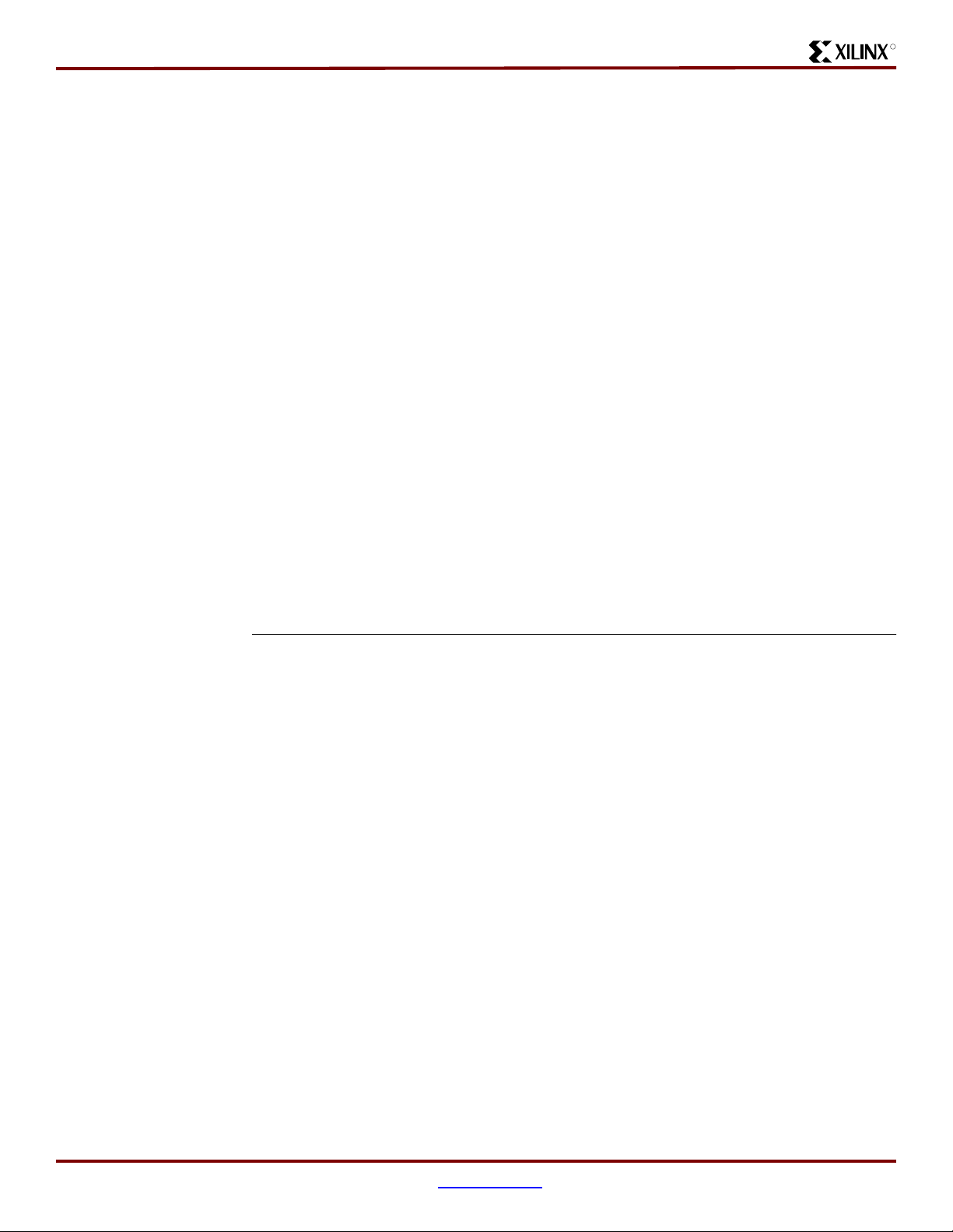
Figure 1 gives an overview of the design. The key features of which are:
• 128 x 128 pixel graphical touch screen.
• USB interface for download music and network connectivity.
• IRDA compliant infrared interface for exchanging data with other units.
• 32 MB of on board FLASH storage.
• CompactFlash interface for storage expansion using CompactFlash cards or MicroDrive
hard drives.
All of this is driven by a high-performance IDT RC32364 32-bit RISC processor and interfaced
using a next generation Spartan-II FPGA. Before the functions implemented in the Spartan
device and the software function running on the RC32364 are examined, the following gives an
overview of the Application Specific Standard Products (ASSPs) that are included in the
design.
2 www.xilinx.com XAPP169 (v1.0) November 24, 1999
1-800-255-7778
MP3 NG: A Next Generation Consumer Platform
R
RC32364
RISC
CPU
USBN9602
USB
Interface
IRQ
IRMS6100
IRDA
Transceiver
8
Addr/Data
Control
3
Control
32
21
3
Xilinx
Spartan II
FPGA
Serial Data
7
Serial Data
2
Serial Data
3
Control Port
2
Serial Audio
3
Data
16
Address
11
Control17
Control
11
Control
9
MT48LC1M16A1
SDRAM
SED1743
LCD Column
Driver
SED1758
LCD Row
Driver
MAX1108
2 Channel
ADC
CS4343
Audio
DAC
KM29U64000T
FLASH
128
128 x 128
4 Wire T ouch
To Stereo
Headphone
Jack
CompactFlash
Interface
LCD Panel
&
Membrane
128
L
R
8
Figure 1: MP3 NG System Block Diagram
IDT RC32364 RISController™
The processor chosen for this design is the IDT RC32364. The features of this device that are
leveraged in this application are:
• Paged memory management unit.
• High-performance, 175 dhrystone MIPs at 133 MHz.
• Integer Multiply ACcumulate (MAC) support, 67M MACs/second at 133 MHz.
• Separate, line lockable, instruction (8 KB) and data (2 KB) caches.
• Power saving features including active power management and a power-down operating
mode.
• On-chip In Circuit Emulation (ICE) interface to provide access to internal CPU state
(registers, cache) and for debug control (breakpoints, single step, insert instructions into
pipeline).
Figure 2 shows the block diagram for this device. The complete data sheet for the RC32364
can be found at the following URL:
http://www.idt.com/docs/79RC32364_DS_32100.pdf
The RC32364’s MMU consists of address translation logic and a Translation Lookaside Buffer
(TLB) capable of supporting demand paged virtual memory. In addition, it includes several
features that are valuable in an embedded application such as variable sized pages and
lockable TLB entries. Figure 3 illustrates the virtual to physical address translation performed
by the RC32364.
XAPP169 (v1.0) November 24, 1999 www.xilinx.com 3
1-800-255-7778
MP3 NG: A Next Generation Consumer Platform
The variable page size lets each mapping independently represent memory regions that can
range from 4 KB to 16 MB. This feature lets the system designer adjust the address mapping
granularity for different memory regions.
Locking TLB entries excludes entries from being recommended for replacement when there is
an address miss. This lets the system designer have mappings for critical regions of code and
or data locked into the TLB for predictable real time performance.
R
8kB
TM
I-Cache,
lockable
RISCore 400 0 Co m pat ible
MMU
System Co ntrol
w/
Coprocessor (CPO)
TLB
2kB D-Cache, 2-set,
lockable, write-back/write-through
RISCore32300 Internal Bus Interface
RC32364 B u s Inter face U n it
Enhanced JTAG (ICE Interface)
RISCore 323 00
Extended MIPS 32
Integer CPU Core
2-set,
Clock
Generation
Unit
Figure 2: RC32364 Block Diagram
Courtesy IDT)
(
Virtual Address with 1M (220) 4-Kbyt e pages
28 11 0
2931
ASID
8
3239
20 bits = 1M
VPN
20 12
12
Offset
Offset passed
unchanged to
physical memory
Offset
Offset pa ssed
unchanged to physical
memory.
0
Bits 31, 30 and 29 of the
virtual address select user, supervisor, or kernel address spaces.
39
ASID
8
8 bits = 256 pages
Virtual Address with 256 (28)16-Mbyte pages
Virtual-to-physical-
translation in TLB
TLB
31 0
32-bit Physical Address
PFN
Virtual-to-
physical transla-
TLB
28 293132
24
VPN
8 24
tion in TLB
23
Offset
Figure 3: RC32364 Address Translation
(Courtesy IDT)
4 www.xilinx.com XAPP169 (v1.0) November 24, 1999
1-800-255-7778
MP3 NG: A Next Generation Consumer Platform
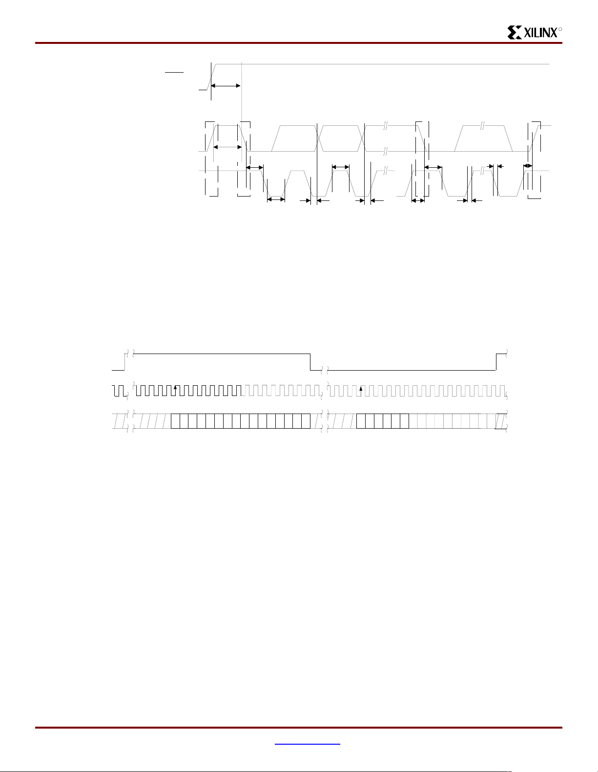
The RC32364 interfaces to the system through a 32-bit multiplexed address/data bus. The bus
offers a rich set of signals to control transfers of which only a subset was required for this
application. Figure 4 shows the timing for read transactions on this bus.
MasterClock
R
AD(31:0)
Addr(3:2)
Width(1:0)
ALE
Rd*
Wr*
CIP*
DT/R*
I/D*
DataEn*
Ack*
Addr
Data Inpu t
Addr
Data In put
Last*
Figure 4: RC32364 Read Timing
(Courtesy IDT)
XAPP169 (v1.0) November 24, 1999 www.xilinx.com 5
1-800-255-7778
MP3 NG: A Next Generation Consumer Platform
R
Crystal CS4343 Stereo DAC
The Digital-to-Analog Converter chosen for this design is the Crystal CS4343 from Cirrus
Logic. This device features:
• 1.8V to 3.3V operation.
• 24-bit conversion at up to 96 kHz.
• Digital volume control.
• Digital bass and treble boost.
• Built-in headphone amplifier capable of delivering 5 mW into a 16
Ω load.
Figure 5 shows the block diagram for this device.
The CS4343 provides three interfaces: the analog stereo headphone interface, the serial port
used to transfer digital audio data streams, and the control port used to configure the device.
RST
VD_IO
LRCK
LK/DEM
SDATA
VA
SERIAL
PORT
DIF1/SDA
DE-
EMPHASIS
DIF0/SCL
CONTROL PORT
DIGITAL
VOLUME
CONTROL
BASS/TREBLE
BOOST
COMPRESSION
LIMITING
DIGITAL
FILTERS
∆Σ
DAC
∆Σ
DAC
ANALOG
FILTER
ANALOG
FILTER
VQ_HP
ANALOG
VOLUME
CONTROL
ANALOG
VOLUME
CONTROL
VA_HP
HEAD-
PHONE
AMPLIFIER
HP
HP
GND FILT+ REF_GND
MCLK
Figure 5: CS4343 Block Diagram
(Courtesy Cirrus Logic)
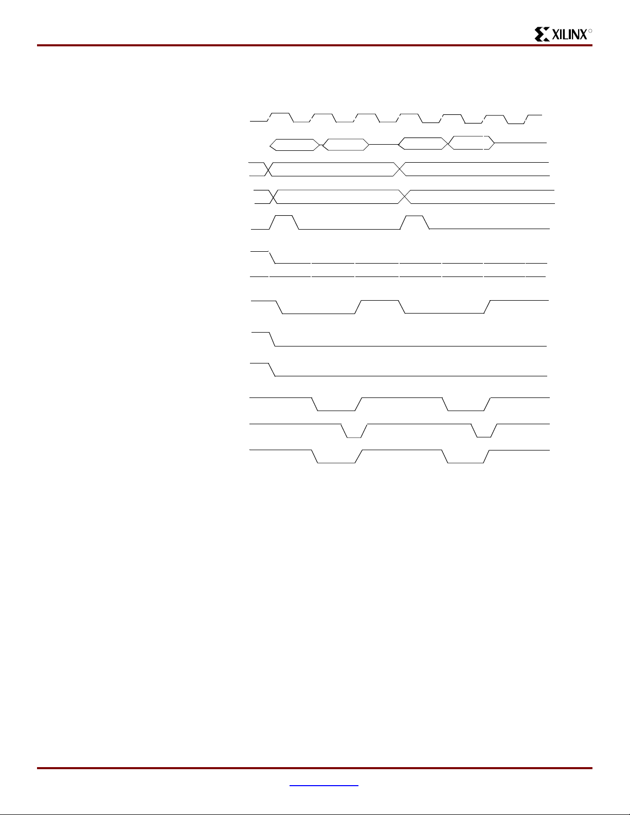
The control port is an industry standard I
2
C slave interface. I2C is a multidrop, 2-wire, serial
interface consisting of a clock (SCL) and data (SDA) and operating at up to 100 kHz. (See
Figure 7 Control Port Timing.) The control port is used to configure device features such as
volume, muting, equalization, power management, and the operating mode of the serial port.
2
Figure 1 on page 3 gives an overview of control port timing. A detailed description of I
2
operation can be found in the I
C specification as described in the references.
C
6 www.xilinx.com XAPP169 (v1.0) November 24, 1999
1-800-255-7778
MP3 NG: A Next Generation Consumer Platform
RST
t
irs
Stop Start
SDA
t
buf
SCL
t
hdst
t
high
Repeated
Start
t
hdst
R
Stop
t
f
t
susp
LRCK
SCLK
SDATA
t
low
t
hdd
t
sud
t
sust
t
r
Figure 6: Control Port Timing
(Courtesy Cirrus Logic)
The serial port can be configured for several operating modes. The mode of operation chosen
for this application is referred to in the CS4343 documentation as "Serial Audio Format 2".
Figure 7 gives an overview of serial port timing when in this mode.
Left Channel
15 14 13 12 11 10
6543210987
15 14 13 12 11 10
Right Channel
6543210987
Figure 7: Serial Port Timing
(Courtesy Cirrus Logic)
XAPP169 (v1.0) November 24, 1999 www.xilinx.com 7
1-800-255-7778
MP3 NG: A Next Generation Consumer Platform
R
Samsung FLASH Memory
The FLASH memory chosen for this design is the KM29U64000T 8M x 8 device from Samsung
Semiconductor. This device is based on NAND FLASH technology and is popular in MP3 player
applications due to its high density and low cost per bit.
Figure 8 shows the block diagram for this device. The complete data sheet for the
KM29U64000T can be found at the following URL:
http://www.usa.samsungsemi.com/products/prodspec/flash/km29u64000(i)t.pdf
Y-Gating
A9 - A22
Command
CE
RE
WE
A0 - A7
X-Buffers
Latches
& Decoders
Y-Buffers
Latches
& Decoders
A8
Command
Register
Control Logic
& High Voltage
Generator
2nd half Page Register & S/A
64M + 2M Bit
NAND Flash
ARRAY
(512 + 16)Byte x 16384
1st half Page Register & S/A
Y-Gating
I/O Buffers & Latches
Global Buffers
Output
Driver
VCCQ
V
SS
I/0 0
I/0 7
CLE ALE WP
Figure 8: KM29U64000T Block Diagram
(Courtesy Samsung Semiconductor)
Unfortunately this device also has two characteristics that present significant system level
design challenges. The first of these is the narrow, highly multiplexed interface that is used to
access the device. The KM29U64000T interfaces to the system through an 8-bit wide port that
is used for both address and data. Figure 9 illustrates the read timing for this device.
The second and most challenging issue relates to data integrity, which is an issue common to
most devices using NAND technology. There are two aspects to this, the first of which is the fact
that devices when shipped may have memory blocks that may not be used due to data errors.
The data sheet for the device has a parameter called N
the device contains. The value of N
varies from device to device and is specified to have a
VB
that is the number valid blocks that
VB
minimum of 1014, a maximum of 1024, and typically 1020. While the first block is guaranteed
to be good, bad blocks can occur at any other location within the memory array . Invalid blocks
are marked at the factory by storing a "0" value at location "0" in either the first or second block
of the page. The system level impact of this is that it must keep track of which blocks are good
within the device and that this results in a non-contiguous memory map.
The second issue is that while the device is guaranteed to provide at least the minimum number
of valid blocks over its operational lifetime these devices may experience failures in additional
blocks throughout their life. In order to ensure system integrity some form of error detection and
correction must be implemented.
The discussion of the FLASH memory interface will discuss how these issues were addressed
in this design.
8 www.xilinx.com XAPP169 (v1.0) November 24, 1999
1-800-255-7778
MP3 NG: A Next Generation Consumer Platform
CLE
CE
tWC
WE
ALE
tWB
R
tCEH
tCHZ
tAR2
tR
tRC
tCRY
tRHZ
RE
I/O0 - 7
R/B
Micron SDRAM Memory
»
tRR
00h or 01h
A0 ~ A 7
Column
Address
A9 ~ A 16
A17 ~ A 22
Page(Row)
Address
Dout N Dout N+1 Dout N+2
Busy
Dout N+3 Dout 527
Figure 9: KM29U64000T Read Timing
(Courtesy Samsung Semiconductor)
The SDRAM memory chosen for this design is the MT48LC1M16A1S - 512K x 16 x 2 bank
device from Micron Semiconductor. This device is available in speed grades from 125 to 166
MHz operating over an LVTTL synchronous interface. Figure 10 shows the block diagram for
this device. Figure 11 shows the MT48LC1M16A1 read timing of the device. The complete data
sheet for the MT48LC1M16 can be found at the following URL:
http://www.micron.com/mti/msp/pdf/datasheets/16MSDRAMx16.pdf
»»
tRB
XAPP169 (v1.0) November 24, 1999 www.xilinx.com 9
1-800-255-7778

MP3 NG: A Next Generation Consumer Platform
R
A0-A10, BA
CKE
WE#
CAS#
RAS#
CLK
CS#
12
DECODE
COMMAND
MODE REGISTER
ADDRESS
REGISTER
CONTROL
LOGIC
12
CONTROLLER
11
REFRESH
REFRESH
COUNTER
(2,048 x 256 x 16)
SENSE AMPLIFIERS
DQM MASK LOGIC
COLUMN
8
DECODER
SENSE AMPLIFIERS
DQM MASK LOGIC
(2,048 x 256 x 16)
BANK0
MEMORY
ARRAY
256 (x16)
I/O GATING
256
256
I/O GATING
256 (x16)
BANK1
MEMORY
ARRAY
DQML,
DQMH
DATA
16
16
OUTPUT
REGISTER
DATA
INPUT
REGISTER
16
8
DQ0DQ15
ROW-
11
8
11
ROW-
ADDRESS
MUX
11
ADDRESS
LATCH
COLUMN-
ROW-
ADDRESS
LATCH
11
ADDRESS LATCH
BURST COUNTER
11
2,048
ROW
DECODER
COLUMN-
ADDRESS BUFFER
2,048
ROW
DECODER
CLK
CKE
COMMAND
DQM
A0-A9
A10
BA
DQ
Figure 10: MT48LC1M16A1 Block Diagram
(Courtesy of Micron Technology, Inc.)
T0 T1 T2 T3 T4 T5 T6 T7 T8
t
CK
t
t
CKH
CKS
t
t
CMH
CMS
3
tAHt
AS
ROW
tAHt
AS
ROW
tAHt
AS
BANK
t
RCD
t
RAS
t
RC
t
CL
t
CH
t
t
CMH
CMS
COLUMN m
2
(A0 - A7)
ENABLE AUTO PRECHARGE
BANK
CAS Latency
NOPNOP NOPACTIVE NOP READ NOP ACTIVENOP
t
AC
t
AC
t
LZ
t
OH
D
OUT
m
t
AC
t
OH
OUT
m + 1
t
AC
t
OH
D
OUT
D
m + 2D
t
RP
ROW
ROW
BANK
t
OH
OUT
m + 3
t
HZ
Figure 11: MT48LC1M16A1 Read Timing
(Courtesy of Micron Technology, Inc.)
10 www.xilinx.com XAPP169 (v1.0) November 24, 1999
1-800-255-7778

MP3 NG: A Next Generation Consumer Platform
R
National Semiconductor USBN9602 USB Function Controller
The USB interface in the design is based on a National Semiconductor USBN9602 controller.
This device, packaged in a 28-pin SOIC package, supports full speed USB function controller
operation and includes an integrated USB transceiver. It contains seven endpoint FIFOs, two of
which are 64 bytes deep.
Figure 12 shows a block diagram of this device. The complete data sheet for the USBN9602
can be found at the following URL:
http://www.national.com/ds/US/USBN9602.pdf
CS RD WR A0/ALE D[7:0]/AD[7:0]
Microcontroller Interface
Endpoint/Control FIFOs
StatusControl
EP2
Endpoint0
EP1
SIE
Media Access Controller
Physi cal Layer Interface
Transceiver
EP4EP3
EP6EP5
(MAC)
(PHY)
VReg
INTR
MODE[1:0]
RESET
Vcc
GND
48 MHz
Oscillator
RX
TX
Clock
Generator
Clock
Recovery
USB Event
Detect
XIN
XOUT
CLKOUT
V3.3
AGND
D+ D-
Upstream Port
Figure 12: USBN9602 Block Diagram
(Courtesy Nationa l Semi c ond uct or )
The system interface for the USBN9602 is a simple 8-bit microprocessor bus that can be
configured to operate in a multiplexed or non-multiplexed mode. The multiplexed mode is more
attractive from a software perspective since it supports random access to the devices’ internal
registers. This mode also reduces the number of interface pins required. For both of these
reasons this was chosen for this application. Figure 13 shows read timing for the USBN9602
when operating in multiplexed mode.
XAPP169 (v1.0) November 24, 1999 www.xilinx.com 11
1-800-255-7778

MP3 NG: A Next Generation Consumer Platform
ALE
CS
RD or WR
R
System Implementation
AD[7:0]
ADDR
DATA
Figure 13: USBN9602 Read / Write Cycle Timing
(Courtesy National Semiconductor)
This section describes how all of these pieces are integrated into a complete system. First
described is the software architecture and the functionality of the key modules. Next is the
architecture and implementation of the logic contained in the Spartan-II FPGA.
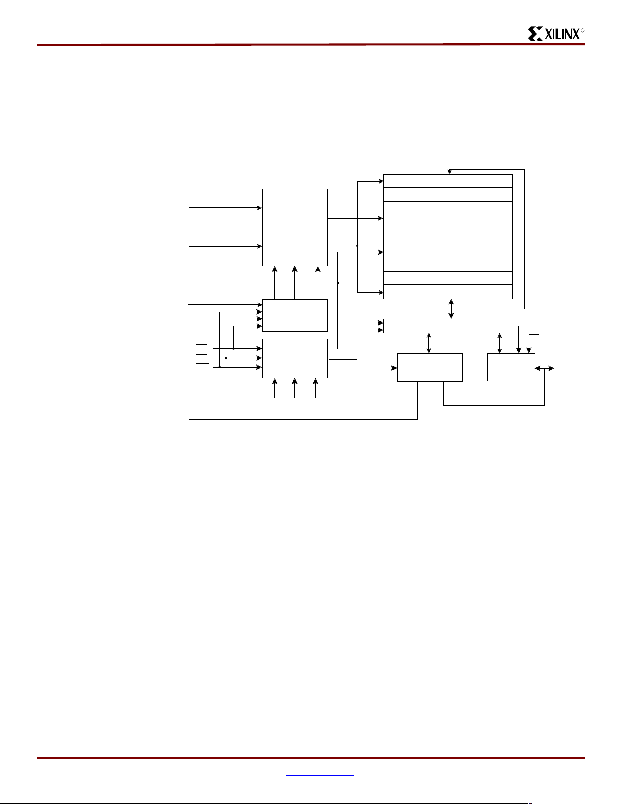
Software Architecture
The system software required to implement this device is shown in Figure 14. The software
components fall into four categories:
• RTOS. A Real Time Operating System is included in the software architecture in order to
simplify the management of resources and concurrent activities.
• BIOS. The Basic Input Output System functions provide low level device management
functions and hardware abstraction.
• Protocol Stacks. These modules implement the network protocol layers for the
communications interfaces.
• Management Processes. These modules implement the application levels functions, and
these run as processes under the RTOS.
12 www.xilinx.com XAPP169 (v1.0) November 24, 1999
1-800-255-7778

MP3 NG: A Next Generation Consumer Platform
UI
Manager
R
RTOS
IRDA
Stack
IR
BIOS
USB
Stack
USB
BIOS
Touch
BIOS
Screen
BIOS
System
Hardware
Decoder
Audio
ISR
Audio
BIOS
MP3
FLASH
BIOS
Memory
Manager
MMU
BIOS
Figure 14: System Software Architecture
The RTOS provides process scheduling and memory allocation functions. The RTOS could be
any of the commercially available packages. Probably more of a factor than any technical issue
is the licensing model for the product. Since this is a product that is targeted at the high-volume,
cost sensitive, consumer market, an RTOS that is licensed on an up front fee basis with no unit
royalties is the most attractive.
The various BIOS components will be discussed later in the sections that describe the
hardware implementation for each interface. The key application modules are as follows:
UI Manager
The User Interface (UI) manager is responsible for handling interaction between the user and
the system. This includes using the Screen BIOS to create the buttons and menus that the user
sees, getting user input through the Touch BIOS and using this information to coordinate
activities such as downloading and playing MP3 files. The UI manager would also spawn
separate processes for value added features such as an appointment calendar, or a phone
book, as needed.
MP3 Decoder and Audio ISR
The MP3 decoder runs as an independent process, controlled by the UI manager. When
activated, it uses the FLASH BIOS to fetch MP3 file data, decompresses it and places the audio
data in a queue. The audio Interrupt Service Routine (ISR) is activated by an interrupt from the
Audio DAC block in the FPGA. When activated, it reads data from this queue and writes it to
FIFOs in the Audio DAC block.
The key to getting optimal performance from the MP3 decoder on the RC32364 lies in taking
advantage of the MAC instruction supported by the processor. The instruction is particularly
valuable in the implementation of the Discrete Cosine Transform (DCT) for sub-band synthesis.
There are several sources for MP3 decoder code. A fixed point decoder (
fixpoint.tgz
) that was developed for the Linux ARM project can be downloaded from the
splay-0.81-
following URL:
ftp://ftp.netwinder.org/users/n/nico
XAPP169 (v1.0) November 24, 1999 www.xilinx.com 13
1-800-255-7778

MP3 NG: A Next Generation Consumer Platform
The reference code that was developed for the standard is available from the Fraunhofer
Institute at the following URL:
A commercial decoder is available from Xaudio. Information on the Xaudio product line is
available from:
Memory Manager
The Memory Manager handles the tasks required to mask NAND FLASH issues from the other
software in the system. Specifically these tasks are block mapping and code initialization.
Block Mapping
This involves maintaining a table of valid FLASH blocks and configuring the MMU to map them
into a linear address space. For the FLASH memory space the TLB entries are set to the same
8 KB size to match the block size of the FLASH itself, and the entries are not locked in the TLB.
A single TLB entry is used to map the SDRAM memory space. This entry is configured to map
a 4 MB memory space and is locked in the TLB.
In the event that an error is detected in a valid block, this code is also responsible for copying
the data to an unused block and marking the block in which the error was detected as bad.
R
http://www.iis.fhg.de/amm/techinf/layer3/index.html
http://www.xaudio.com
Xilinx Spartan- II FPGA
Code Initialization
This function copies the code image from FLASH to RAM at boot time. This routine must also
perform error detection on the image as it is copied. If an error is detected, error correction must
be performed and the block mapping code informed.
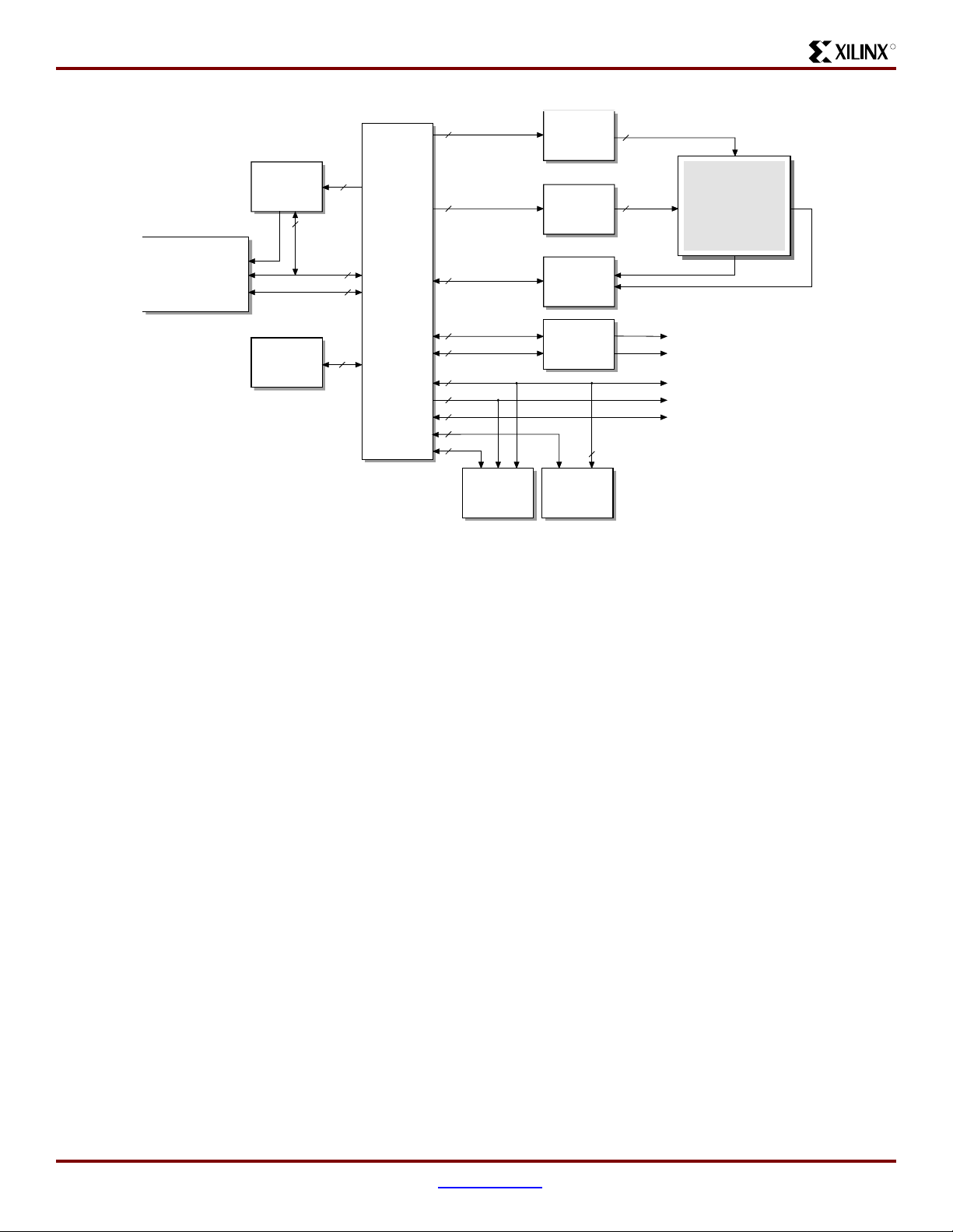
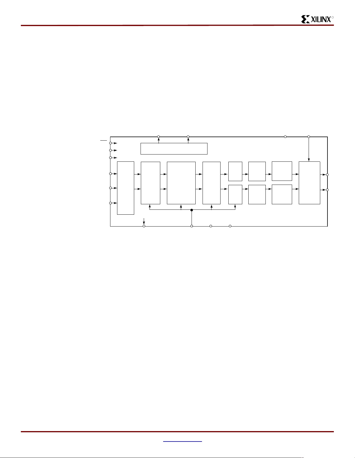
Figure 15 shows the architecture implemented in the Spartan-II device for this application. It
consists of eight major functional blocks:
• IP Bus Controller
• CPU Interface
• LCD Controller
• Memory Datapath
• SDRAM Controller
• FLASH Controller
• CompactFlash Controller
• IRDA Controller
• DAC Interface
• Touch Screen Interface
These blocks are interconnected by a simple non-multiplexed, multi-master, address data bus
that is referred to as the IP bus. While the IP bus may appear to be a bus to the function blocks,
it is not a bus at all but instead uses multiplexers for gating data into the internal datapaths. This
approach eliminates the need for 3-state drivers within the design. In this implementation the
bus has two masters; the CPU Interface and the LCD Controller. Figure 15 shows a top level
block diagram of the FPGA.
14 www.xilinx.com XAPP169 (v1.0) November 24, 1999
1-800-255-7778

MP3 NG: A Next Generation Consumer Platform
CPU Interface
CPU Address/Data
CPU Control
USB Control
D_OUT[31:0]
D_IN[31:0]
A_OUT[31:2]
Control Out
MUX
MUX
LCD Controller
D_IN[31:0]
A_OUT[31:2]
Control Out
DAC Interface
D_OUT[31:0]
D_IN[31:0]
A_IN[3:2]
Control In
Touch Screen
Interface
D_OUT[31:0]
D_IN[31:0]
A_IN[3:2]
Control In
LCD Control
Signals
DAC Interface
Signals
ADC Interface
Signals
R
Tranceiver Interface
Signals
IRDA Controller
D_OUT[31:0]
D_IN[31:0]
A_IN[3:2]
Control In
MUX
Memory Interface
D_OUT[31:0]
D_IN[31:0]
A_IN[19:0]
Control In
SDRAM Controller
Control In
FLASH Controller
Control In
CompactFlash
Controller
Control In
Memory Data
Memory Address
SDRAM Control
Signals
FLASH Control
Signals
CompactFlash
Control
Signals
Figure 15: FPGA Logic Block Diagram
While most of the blocks are fairly independent, the FLASH, SDRAM, and CompactFlash
interfaces share common address and data busses. While this results in a fairly complex
muxing scheme for these datapaths it is necessary to keep the pin count within an acceptable
range.
The following sections will discuss the implementation of each of these functional blocks and
outline the hardware and software resources needed to support each.
IP Bus Controller
The IP Bus Controller block performs two functions: block address decoding and IP bus
arbitration.
The address decode block generates device selects for the IP block that is the target of the
transfer. It also controls the multiplexers that select the response signals from the target of the
transfer (ACK, DOUT, etc.).
IP bus arbitration between access requests from the CPU Interface and the LCD Controller are
handled by using a simple rotating priority scheme. The arbiter block also controls the
multiplexers that select which set of transfer control signals (RD, WR, etc.) control the transfer.
The FPGA device resources used to implement this block include an estimated 32 CLBs but no
I/O pads. There is no software required to support this block.
XAPP169 (v1.0) November 24, 1999 www.xilinx.com 15
1-800-255-7778

MP3 NG: A Next Generation Consumer Platform
CPU Interface
The CPU Interface block performs three functions: protocol conversion, CPU initialization and
address de-multiplexing. Figure 16 shows a block diagram of this block.
CPU_COLDRESET_N
CPU_BUSGNT_N
CPU_MASTERCLK
CPU_RESET_N
CPU_INT_N[3:0]
CPU_AD[31:0]
CPU_ALE
CPU_ADDR[3:2]
CPU_CIP_N
CPU_BE_N[3:0]
CPU_RD_N
CPU_WR_N
CPU_ACK_N
USB_CS_N
USB_RD_N
USB_WR_N
CPU
Initialization
28
Bus State
Machine
Latch
DQ
Enable
IR_INT_N
DAC_INT_N
SYS_CLK
DIN[31:0]
DOUT[31:0]
28
AOUT[31:4]
2
AOUT[3:2]
SYS_CLK
RD_OUT_N
WR_OUT_N[3:0]
ACK_IN
REQ_OUT
GNT_IN
R
Figure 16: CPU Interface Block Diagram
The CPU initialization block generates the required timing for the reset signals and drives
configuration informat ion onto bu s grant and the int er ru pts. Thi s conf ig urati on info r mati on
configures the boot PROM width and enables the CPU timer. After initialization is complete the
block drives the IRDA and audio DAC interrupts out onto the CPU interrupt signals.
The bus sta te m achin e conv erts t he si gnali ng on the C PU bus into the fo rmat used on th e local
IP bus, or if the transaction is to the USB interface, the signaling accepted by the USBN9602.
The FPGA device resources used to implement this block include an estimated 46 CLBs and
the 54 I/O pads listed in Table 1.
16 www.xilinx.com XAPP169 (v1.0) November 24, 1999
1-800-255-7778

MP3 NG: A Next Generation Consumer Platform
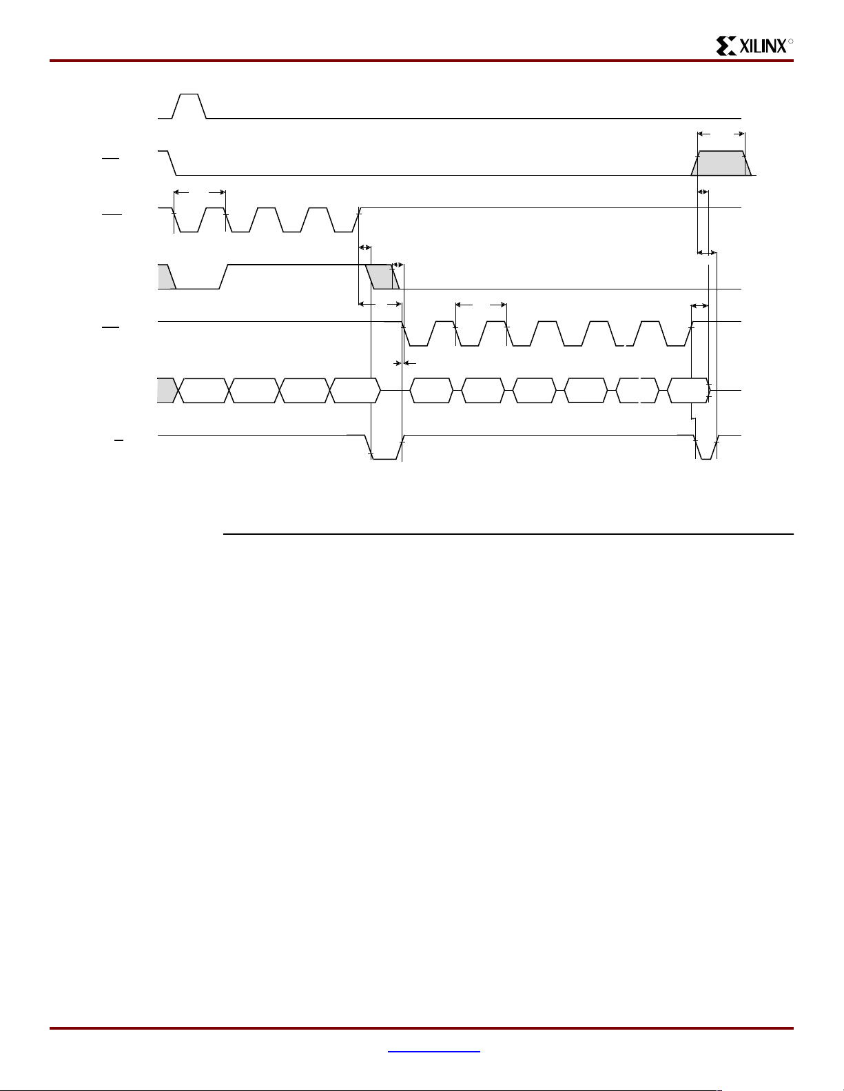
Table 1: CPU Interface Signal Summary
Signal T ype Description
CPU_MASTERCLK Output All bus timing is relative to this clock. The CPU core frequency is derived by
multiplying this clock.
CPU_AD[31:0] I/O High-order multiplexed address and data bits.
CPU_ADDR[3:2] Input Non-multiplexed address lines. These serve as the word within block address for
cache refills (Addr[3:2]).
CPU_BE_N[3:0] Input Indicates which byte lanes are expected to participate in the transfer.
CPU_ALE Input Address latch enable.
CPU_CIP_N Input Denotes that a cycle is in progress. Asserted in the address phase and is asserted
until the ACK* for the last data is sampled.
CPU_RD_N Input This active Low signal indicates that the current transaction is a read.
CPU_WR_N Input This active Low signal indicates that the current cycle transaction is a write.
CPU_BUSGNT_N Output During the power-on reset (Cold Reset), BusGnt* is an input and is used to load
ModeBit(5).
R
CPU_ACK_N Output On read transactions, this signals the RC32364 that the memory system has placed
valid data on the A/D bus, and that the processor may move the data into the on-
chip Read Buffer. On a write transaction, this signals to the RC32364 that the
memory system has accepted the data on the A/D bus.
CPU_RESET_N Output This active Low signal is used for both power-on and warm reset.
CPU_COLDRESET_N Output This active Low signal is used for power-on reset.
CPU_INT_N[3:0] Output Active Low interrupt signals to the CPU. During power-on,
Int*(3:0)serves as
ModeBit(9:6).
US_CS_N Output USB controller chip select.
US_RD_N Output USB controller read strobe.
US_WR_N Output USB controller write strobe.
There is no direct software support required for this block, but the USB interface itself requires
considerable software for operation. This software consists of the USB protocol stack, which
includes a USB interrupt service routine. The USB stack itself consists of two parts. The first of
these is the software required for participating in the USB protocol and the plug and play. The
second part is the application specific code required to transfers MP3 files from the host system
to the player.
LCD Controller
The LCD Controller is responsible for refreshing the screen with an image stored in the
SDRAM. In general its operation is similar to that of a CRT display controller. Unlike most
display controllers, the display format generated by the LCD controllers is not programmable by
the CPU. The raster format is fixed at 128 x 128 pixels and the display timing is fixed as well.
This makes sense in an embedded system such as this where the display is integrated into the
unit. Although the display format cannot be changed in the system, loading different FPGA
configurations into the FLASH when the unit is manufactured can accommodate different
displays. Figure 17 shows the block diagram of the LCD Controller.
XAPP169 (v1.0) November 24, 1999 www.xilinx.com 17
1-800-255-7778

MP3 NG: A Next Generation Consumer Platform
DIN[31:0]
SYS_CLK
BREQ_N
BGNT_N
RD_N
ACK_N
AOUT[10:2]
32
9
FIFO
DQ
RdWr
Address
Counter
9
DQ
Enable
Load
32
State
Machine
9
Shift
Register
DQ
Enable
Load
4
R
DI_D[3:0]
DI_XSCL
DI_LP
DI_FR
DI_YD
DI_YSCL
AOUT[31:11]
21
Base
Address
Figure 17: LCD Controller Block Diagram
The LCD Controller is an IP bus master and fetches data for screen refresh independently of
CPU activities. The display data that is fetched is loaded into a FIFO using a block transfer
across the IP bus. The shift register loads display data from the FIFO and shifts it out as a 4-bit
wide data stream at 16 MHz the maximum shift rate supported by the display drivers.
In order to prevent disruption of the display image, the FIFO must have a new data word
available for the shift register every time it empties. This occurs every 500 ns (1 / [16 MHz / 8]).
Since there is a significant amount of overhead associated with each non-sequential access to
the SDRAM memory, fetches are made from it using multi-word bursts. The size of these bursts
is a compromise between different factors. Longer bursts are more efficient since the SDRAM
access overhead is amortized over a larger number of data words. Smaller bursts reduce the
size of the FIFO and also reduce bus latency by reducing the time that the LCD controller ties
up the IP bus. For this application a 2-word burst was chosen. The result is a 3-word deep FIFO
and display buffer fetches every 1
µs.
The FPGA device resources used to implement this block include an estimated 58 CLBs and
the nine I/O pads listed in Table 2.
Table 2: LCD Controller Interface Signal Summary
Signal Type Description
DI_XD[3:0] Output X driver data
DI_XSCL Output X driver data shift clock
DI_LP Output Latch pulse
DI_FR Output Frame signal
DI_YD Output Y driver scan start pulse
DI_YSCL Output Y driver shift clock
18 www.xilinx.com XAPP169 (v1.0) November 24, 1999
1-800-255-7778

MP3 NG: A Next Generation Consumer Platform
The only software support required for this block is the screen BIOS which consists of functions
to generate screen images by manipulating the frame buffer memory . This buffer appears as an
array of 512, 32-bit words with each word containing 32 pixels of the screen image. The most
significant bit of the word at the base address appears as the pixel in the upper left-hand corner
of the screen. The least significant bit of that memory word appears as the 32
row. The word and bit address of any pixel on the screen can be calculated using the following
formula:
nd
pixel in the first
R
Memory Address
Bit Address
= X * Y MOD 32
= X * Y REM 32
Where:
X and Y are the horizontal and vertical coordinates of the screen and
assume that the origin (X = 0, Y = 0) is in the upper left-hand corner of the screen.
MOD the integer division.
REM is the remainder of the division
Memory I nterface
The memory interface block, Figure 18 implements the data path required to map the 8- and
16-bit memory devices to the 32-bit IP bus. While the RC32364 is capable of fetching instructions and data from devices with varying bus widths, having the FPGA build 32-bit words for the
CPU reduces the number of bus cycles. This increases performance and also reduces power
consumption. Figure 16 on page 16 shows a block diagram of this block.
A_IN[19:9]
A_IN[8:1]
A_IN[10:0]
D_IN[31:24]
D_IN[23:16]
D_IN[15:8]
D_IN[7:0]
MUX
MEM_DOUT[15:8]
MUX
MEM_DOUT[7:0]
MUX
MEM_ADDR[10:0]
D_OUT[31:24]
D_OUT[23:16]
D_OUT[15:8]
D_OUT[7:0]
MUX
Register
QD
Register
QD
Register
QD
MUX
MEM_DIN[15:8]
MEM_DIN[7:0]
MEM_D[15:0]
Figure 18: Memory Interface Block Diagram
XAPP169 (v1.0) November 24, 1999 www.xilinx.com 19
1-800-255-7778

MP3 NG: A Next Generation Consumer Platform
SDRAM Controller
The SDRAM controller design (Figure 19) is based on the design developed by Xilinx in
application note XAPP134: Virtex Synthesizable High Performance SDRAM Controller. The
changes made in the original design are to adapt to the differences in the host interface. In the
original design the host interface is a multiplexed address data bus. In this application the IP
bus is non-multiplexed. Another difference is that the original design supported a 32-bit wide
memory configuration with two MT48LC1M16 memory devices. In the design a 16-bit wide
memory datapath and a single MT48LC1M16 is used.
SYS_CLK
SDRAM_SEL_N
ACK_N
WR_IN_N[3:0]
RD_IN_N
Figure 19: Figure 19 SDRAM Controller Block Diagram
State
Machine
sdrm_t.v from XAPP 134
State
Machine
Refresh
Counter
32
R
SD_BA
SA_CS
SD_CLK
SD_CKE
SD_RAS
SD_CAS
SD_WE
SD_DQML
The estimated FPGA device resources used to implement this block include an estimated 100
CLBs, two DLLs, two global clock buffers and the nine I/O pads listed in Table 3. There is no
software support required for this block.
T able 3: SDRAM Controller Interface Signal Summary
Signal Type Description
SD_BA Output Bank address
SD_CS Output Chip select
SD_CLK Output Transfer clock
SD_CKE Output Clock enable
SD_RAS Output Row address strobe
SD_CAS Output Column address strobe
SD_WE Output Write enable
SD_DQML Output Lower byte data mask
SD_DQMH Output Higher byte data mask
FLASH Controller
The largest cost associated with this design is the large amount of FLASH memory, 32 MB or
more, that is required for storing MP3 audio files. In order to leverage this cost it is desirable to
use this memory for all non-volatile storage requirements within the system. This includes code
storage for the CPU as well as storage of the MP3 audio stream. (See Figure 20.)
20 www.xilinx.com XAPP169 (v1.0) November 24, 1999
1-800-255-7778

MP3 NG: A Next Generation Consumer Platform
R
Device decodes
from
IP Bus Controller
SYS_CLK
FLASH_SEL_N
ACK_N
WR_IN_N[3:0]
RD_IN_N
State
Machine
FL_CE_N[3:0]
FL_ALE
FL_WE_N
FL_RE_N
FL_SE_N
FL_WP_N
FL_R/B_N
Figure 20: FLASH Controller Block Diagram
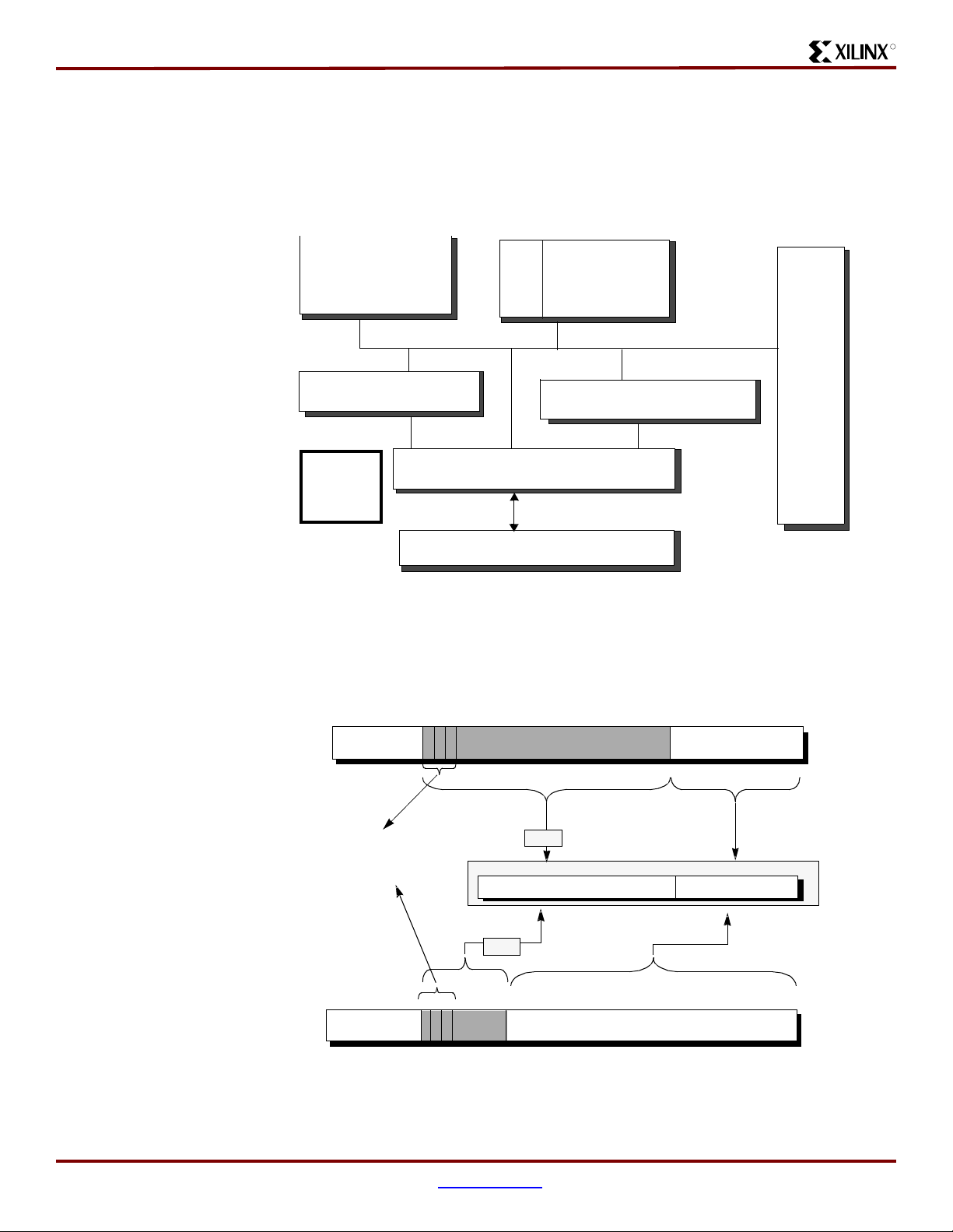
When the architecture for this system was being planned, one issue that needed to be
addressed was whether to execute the program image directly from FLASH or to copy it to
SDRAM. There were two key issues that needed to be considered when making this decision.
Performance
The narrow, 8-bit, interface used for both address and data is one performance issue, but it is
not the biggest. The real problem is random access latency. Within a 512-byte memory page,
data can be read with a 50 ns read cycle time. The problem comes when the processor
accesses data on a different page. The time required to load a page into the page register,
where it can be accessed, is 7
µs. With a 66 MHz processor frequency this represents 462
instruction times. This latency will adversely effect real-time performance.
Error Handling
Each 512-byte page in the FLASH has 16 bytes of spare storage for storing ECC information.
The problem is that this is not enough storage for implementing ECC for small block sizes. For
example, to correct single bit errors on an RC32364 cache line (16 bytes) using a Hamming
code the following relationship must be satisfied:
≤ 2**K – K – 1
N
where: N is the number of data bits in the block
K is the number of ECC bits
Solving for K:
16 * 8 = 256
≤ 2K – K – 1
K = 9 ECC bits per cache line
Since there are 32 (512/16) cache lines per page, a total of 36 bytes are needed for ECC
storage. Recall that 16 bytes are available.
In order to get around this problem, the block size could be increased to 32 bytes. At 32 bytes,
ten bits of ECC are required per block, but there are now only 16 blocks per page which is
consistent with the available ECC memory per page. Performing the block check over two
cache lines could accommodate this larger block size. The down side to this is that every time
a cache line is loaded, two would have to be checked with a corresponding increase in memory
latency.
As a result of this the decision was made to copy the executable image to the SDRAM memory
at boot time. This not only increases performance but also turns the ECC checking issue into a
non real-time software exercise.
The estimated FPGA device resources used to implement this block include an estimated 100
CLBs, and the ten I/O pads listed in Table 4.
XAPP169 (v1.0) November 24, 1999 www.xilinx.com 21
1-800-255-7778

MP3 NG: A Next Generation Consumer Platform
Table 4: FLASH Controller Interface Signal Summary
Signal Type Description
FL_CE_N[3:0] Output Device chip enables, active Low.
FL_ALE Output Address latch enable.
FL_WE_N Output Write enable, write data is latched on the rising edge.
FL_RE_N Output Read enable, when Low enables device data output buffers.
FL_SE_N Output Enable spare area when Low.
FL_WP_N Output Write protect, act iv e Low.
FL_R/B_N Input Open drain output from devices, pulled Low when a program,
Software support required for this block consists of the FLASH BIOS which implements low
level primitives for programming, erasing, and checking validity of memory blocks.
IRDA Controller
R
erase, or read operation is in progress.
The IRDA controller is essentially a specialized, fixed function UART. The separate, 2-word,
transmit and receive FIFOs reduce the interrupt overhead associated with data transmission.
At the maximum data rate that the IR transceiver can support (115 kb/s) the CPU will get an
interrupt every 557 ms. (See Figure 21.)
.
Tx State
Machine
Shift
D_IN[31:0]
SYS_CLK
INT_N
RD_IN_N
WR_IN_N[3:0]
ACK_N
D_OUT[31:0]
FIFO
32
32
DQ
FIFO
QD
32
Bus State
Machine
32
Register
DQ
Shift
Register
QD
MUX
IR_TXD
IR_RXD
Rx State
Machine
Figure 21: IRDA Controller Block Diagram
22 www.xilinx.com XAPP169 (v1.0) November 24, 1999
1-800-255-7778

MP3 NG: A Next Generation Consumer Platform
Table 5: Table 5 IRDA Transceiver Interface Signal Summary
Signal T ype Description
IR_TXD Output Transmit data
IR_RXD Input Receive data
IR_SD Output Shut down signal, puts transceiver into low power mode
Audio DAC Interface
The interface for the CS4343 consists of two separate functional blocks, one for each of the
serial interfaces that are required to support this device. Figure 22 shows a block diagram of
this interface.
32
FIFO
DQ
32
Shift
Register
DQ
R
D_IN[31:0]
SYS_CLK
INT_N
RD_N
WR_N
ACK_N
D_IN[31:0]
D_OUT[31:0]
32
32
32
FIFO
DQ
State
Machine
Register
DQ
32
Shift
Register
DQ
2
MUX
DAC_SDATA
DAC_MCLK
DAC_LRCK
DAC_SCL
DAC_SDA
Figure 22: Audio DAC Interface Block Diagram
The control port interface is implemented as a 2-bit I/O port that is manipulated by software in
order to implement the I
2
C protocol used for accessing the control and status registers in the
DAC. This approach uses minimal device resources and is practical due to the low data rate of
this port and its infrequent use.
When the system is in operation, the serial audio port is in use most of the time. Therefore,
dedicated hardware is provided for implementing the transfer protocol and for delivering an
uninterrupted audio stream. This hardware consists of two, 4-word FIFOs, one for each audio
channel and a state machine to manage the FIFOs and sequence the interface signals.
XAPP169 (v1.0) November 24, 1999 www.xilinx.com 23
1-800-255-7778

MP3 NG: A Next Generation Consumer Platform
Like the IRDA controller, an interrupt is generated every time the FIFOs transfer their last word
into the shift registers. Assuming a 48 kHz audio sampling rate, this will result in an interrupt
every 83.3
µs. To put this in perspective, this means that the CPU will get an interrupt every
5,333 instructions.
Table 6: Audio DAC Interface Signal Summary
Signal Type Description
DAC_MCLK Output Master clock
DAC_LRCK Output Left / Right clock, determines which channel is currently being
DAC_SDATA Output Serial audio data
DAC_SCL Output I
DAC_SDA I/O I
Touch Screen Interface
The touch screen interface is an I/O port that lets the processor read the data returned by a
two-channel analog-to-digital converter. This lets the system software read the X and Y
coordinate resistance values that result from the user touching the screen. The system
software handles linearization and filters out transient touch events. (See Figure 23 and
Table 7.)
transferred
2
C data clock
2
C data
R
Register
D_IN[31:0]
D_OUT[31:0]
32
32
DQ
Figure 23: Touch Interface Block Diagram
Table 7: Touch Screen Interface Signal Summary
Signal T ype Description
AD_SCK Output Serial data clock
AD_SDI Input Serial data in
AD_SDO Output Serial data out
3
AD_SCK
AD_SDI
AD_SDO
24 www.xilinx.com XAPP169 (v1.0) November 24, 1999
1-800-255-7778

MP3 NG: A Next Generation Consumer Platform
R
Spartan Device Selection
Spartan devices are available in a range of densities and packages. The following criteria were
used to select the device used in this application:
• I/O Pins. The design requires a total of 137 I/O pins. I/O pin requirements per block are
summarized in FPGA Resource Usage Summary.
• Voltage. The design operates at 3.3V.
• Density. The estimated
Table 8.
• Performance. The highest clock speed used in the device is 64 MHz, used to clock the
SDRAM controller state machines. The remaining logic runs at sub multiples of this clock
rate.
• Packaging. The size constraints imposed on most modem designs dictates a high-density
surface mount package.
Based on these criteria the device selected for this design is the XC2S100. This device offers
100K gates density, 3.3V operation, 176 user I/O, and is packaged in a space saving FG256
BGA package.
Table 8: FPGA Resource Usage Summary
Interface CLB Usage Number of Signals
CPU 25 51
LCD Display 58 9
size of the design is 83,000 gates, with the usage broken out in
IRDA 59 3
USB 21 3
DAC 23 5
ADC 0 3
SDRAM 100 9
FLASH 100 10
CompactFlash 100 17
Memory Address Bus 4 11
Memory Data Bus 10 16
Total: 500 137
Conclusion The design that has been outlined meets both original design objectives. Even with budgetary
pricing the cost of the solution is well below $100. T able 9 shows the cost breakdown of the
system. The design also has enough spare resources both in terms of CPU cycles and FPGA
gates to support field upgrades. Operating at a core clock speed of 64 MHz, the RC32364 will
provide enough performance for both audio decoding and user interface functions. By locking
the audio decode functions in the instruction cache a significant increase in system
performance as well as reduced power consumption is achieved.
This design also illustrates how manufacturers can create designs that the optimized
integration of an ASIC while supporting the manufacturing and field upgrade flexibility of an
FPGA.
XAPP169 (v1.0) November 24, 1999 www.xilinx.com 25
1-800-255-7778

MP3 NG: A Next Generation Consumer Platform
Table 9: NG Player Semiconductor BOM
Item Qty. Mfg.
Part
Number Description Volume
Unit
Cost
1 4 Samsung KM29U6400T Flash, 64Mb 1M/Yr. $10.00 $40.00
R
Ext.
Cost.
2 1 Micron Mt48C1LC1M16A1TG7SIT SDRAM,
200K/m $3.50 $3.50
512K x 16 x 2 banks
3 1 IDT RC32364-133 RISC CPU 100K $11.50 $11.50
4 1 Xilinx XC2S100 FPGA 20K/m $10.00 $10.00
5 1 Xilinx XC1801 Serial Configuration
20K/m $3.00 $3.00
PROM
6 1 NSC USB9602 USB Interface Controller 20K/m $1.63 $1.63
7 1 SMOS SED1758T0A LCD Common Driver,
20K/m $2.50 $2.50
160 Rows
8 1 SMOS SED1743T0A LCD Segment Driver,
20K/m $2.50 $2.50
160 Columns
9 1 Various TBD 160 x 160 LCD Panel,
est. $5.00 $5.00
Glass Only
10 1 MicroTouch TBD Touch Screen est. $5.00 $5.00
11 1 Infineon IRDT6100 1Mb IRDA Transceiver 20K/m $2.00 $2.00
12 1 Crystal CS4343 DAC Stereo Audio est $2.00 $2.00
13 1 Maxim MAX1108 AD Converter disti $2.68 $2.68
14 1 Maxim MAX1705 Step-up DC to DC
10K $2.81 $2.81
Converter
Notes: BOM includes only semiconductor content.
Total: $94.12
References RC32364 RISController, Hardware User’s Manual, April 1999, Integrated Device Technology
Xilinx Spartan-II FPGA Data Sheet, January 2000, Xilinx
IRMS6100 1.15 Mb/s IrDT Data Transceiver Data Sheet, May 1999, Infineon Technologies
SED1743 160-bit LCD Common Driver Data Sheet, Epson Electronics
SED1758 160-bit LCD Segment Driver Data Sheet, Epson Electroni c s
CS4343 Low Voltage, Stereo DAC with Headphone Amp Data Sheet, June 1999, Cirrus Logic
MAX1108 2-Channel, Serial 8-bit ADC, Data Sheet, October 1998, Maxim Integrated Products
USBN9602 Full Speed Function Controller With DMA Support Data Sheet, May 1998, National
Semiconductor
MT48LC1M16A1 S - 512K x 16 x 2 banks Synchronous DRAM Data Sheet, August 1999, Micron
Technologies
KM29U64000T 8M x 8 bit NAND Flash Memory, April 1999, Samsung Semiconductor
26 www.xilinx.com XAPP169 (v1.0) November 24, 1999
1-800-255-7778

MP3 NG: A Next Generation Consumer Platform
R
Revision History
Date Version # Revision
11/24/99 1.0 Initial release.
© 1999 Xilinx, Inc. All rights res erved. All Xili nx tradema rks, registe red trademar ks, patents, and disclaimers are as listed at http://www.xilinx.com/legal.htm
the property of their respective owners.
. All other trademarks a nd regist ered trademark s are
XAPP169 (v1.0) November 24, 1999 www.xilinx.com 27
1-800-255-7778
 Loading...