

Page 1

Application Note: Embedded Processing
R
Reference System: OPB IIC Using the
ML403 Evaluation Platform
XAPP979 (v1.0) February 26, 2007
Summary This application note describes how to build a reference system forthe On-Chip PeripheralBus
Inter IC (OPB IIC) core using the IBM PowerPC™405 Processor (PPC405) based embedded
system in the ML403 Embedded DevelopmentPlatform. The reference system is Base System
Builder (BSB) based.
An IIC primer is given and an OPB IIC register referenceis provided. The Xilinx Microprocessor
Debugger (XMD) commands are used for verifying that the OPB IIC core operates correctly.
Severalsoftware projects illustrate how to configure the OPB IIC core, set up interrupts, and do
read and write operations. Some of the software projects interface the OPB IIC to the
MicroChip 24LC04B serial EEPROM with an IIC interface, while others interface to the
TotalPhaseAardvark Adapter,which providesIIC masterandslavefunctionality.The procedure
for using ChipScope™ to analyze OPB IIC functionality is provided. The steps used to build a
Linux kernel using MontaVista are listed. Simulation output files for analyzing basic IIC
transactions are provided.
Included Systems
This application note includes one reference system:
www.xilinx.com/bvdocs/appnotes/xapp979.zip
Author: Paul Glover, Ed Meinelt, Lester Sanders
Required Hardware/Tools
The project name used in xapp979.zip is ml403_ppc_opb_iic.
Users must have the following tools, cables, peripherals, and licenses available and installed:
• Xilinx EDK 8.2.02i
• Xilinx ISE 8.2.03
• Xilinx Download Cable (Platform Cable USB or Parallel Cable IV)
• Monta Vista Linux v2.4 Development Kit
• Modeltech ModelSim v6.1d
• ChipScope v8.2
© 2007 Xilinx, Inc. All rights reserved. All Xilinx trademarks, registered trademarks, patents, and further disclaimers are as listed at http://www.xilinx.com/legal.htm. PowerPC is
a trademark of IBM Inc. All other trademarks and registered trademarks are the property of their respective owners. All specifications are subject to change without notice.
NOTICEOF DISCLAIMER: Xilinx is providing this design, code, or information "as is." By providing the design, code, or information as one possible implementation of this feature,
application, or standard, Xilinx makes no representation that this implementation is free from any claims of infringement. You are responsible for obtaining any rights you may
require for your implementation. Xilinx expressly disclaims anywarranty whatsoeverwith respect to the adequacy of the implementation, including but not limited to any warranties
or representations that this implementation is free from claims of infringement and any implied warranties of merchantability or fitness for a particular purpose.
XAPP979 (v1.0) February 26, 2007 www.xilinx.com 1
Page 2
Introduction
Introduction This application note accompanies a referencesystem built on the ML403 development board.
Figure 1 is a block diagram of the reference system.
R
OPB
INTC
PowerPC™
405 Processor
PLB
DDR
OPB UART
16550
PLB
BRAM
OPB
IIC
OPB
PLB
X979_01_022307
Figure 1: OPB IIC Reference System Block Diagram
The system uses the embedded PowerPC(PPC) as the microprocessor and the OPB IIC core.
IIC Primer
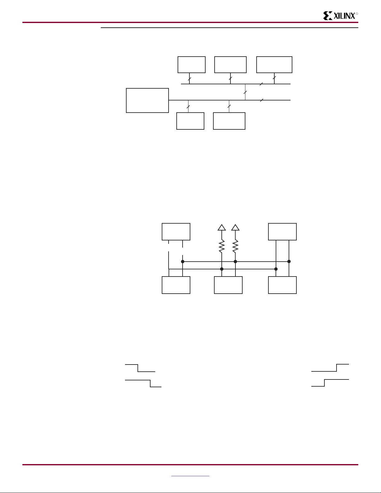
Figure 2 shows components on an IIC bus.Two IIC masters and three IIC slaves are shown.
The master is responsible for setting up transactions. This includes generating the clock on
SCL and defining which slave is involved in the communication, with an address field, and
which component is transmitting and which component is receiving. Some components are
slave only, while others can transition between master and slave operation.
M1 M2
SCL
SDA
S1 S2
S3
X979_02_022307
Figure 2: IIC Bus
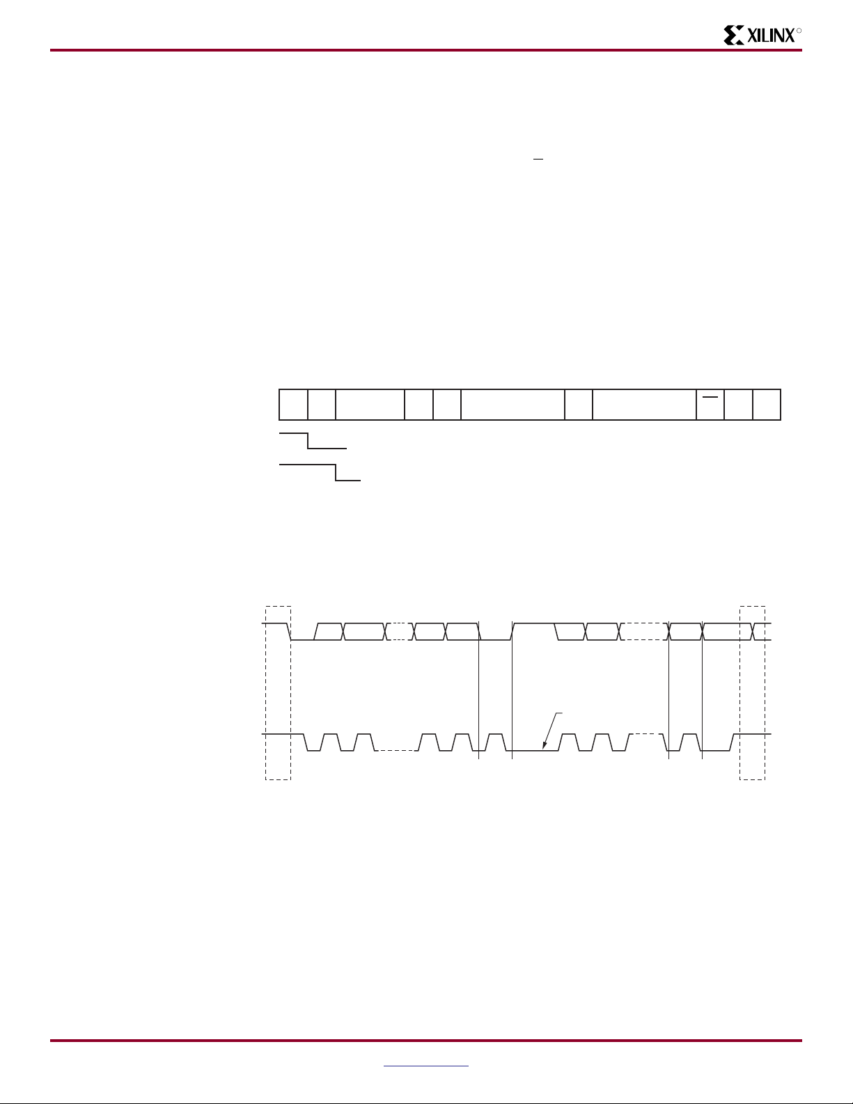
Figure 3 shows the START and STOP conditions. A START condition is a falling edge on SDA
when SCL is high. A STOP condition is a rising edge on SDA when SCL is high. During data
transfer, the data line is stable on SDA when SCL is high. Data transitions on SDA when SCL
is low. Note that the START and STOP conditions are special conditions, violating the rule that
data cannot transition while SCL is high.
SDA
SCL
Start Stop
X979_03_022307
Figure 3: Start and Stop Conditions
XAPP979 (v1.0) February 26, 2007 www.xilinx.com 2
Page 3
Introduction
R
Figure 4 shows the format of the data transfer of two bytes on the IIC bus, beginning with the
START (S) condition and ending with the STOP (P) condition, bounded by an idle IIC (F) bus.
After a START condition, an eight bit field is transmitted containing a 7 bit address and a single
Read/Write (R/W) bit. This 8 bit address/direction field is followedby an Acknowledge bit. After
the address/data field, an eight bit data field is followed by an acknowledge bit (A). The last 8bit data field is followed by a not acknowledge bit (A). This is followed by the STOP condition
(P).
A single message can contain multiple startconditions, or a repeated start, without intervening
STOP conditions.
In this data transfer, there are two acknowledge bits and one Not Acknowledge on the IIC bus.
The distinction between a Not Acknowledge and a No Acknowledge is that Not Acknowledge
occursafter a master has read a byte from a slave and a No Acknowledgeoccurs aftera master
has written a byte to a slave.
A synchronized SCL is generated with its LOW period determined by the device with the
longest low period and its HIGH period determined by the device with the shortest HIGH
period.
FAAR/WS PF
Slave
Address
Data Data
A
SDA
SCL
X979_04_012907
Figure 4: Data Transfer on the IIC Bus
Figure 5 shows the data transfer on the IIC bus, beginning with the START condition and
ending with the STOP condition.
P
SDA
Sr
Sr
or
P
STOP or
repeated START
condition
X979_05_022307
SCL
S
or
SR
START or
repeated START
condition
MSB
12 127 8 9 3 - 8 9
Acknowledgment
signal from slave
Byte complete;
interrupt within slave
Clock lines held low while
interrupts are serviced
Acknowledgment
signal from receiver
ACKACK
Figure 5: Generic Data Transer on the IIC Bus
XAPP979 (v1.0) February 26, 2007 www.xilinx.com 3
Page 4

Reference System Specifics
R
Figure 6 shows the acknowledge bit on the IIC bus.
Data output
by transmitter
Data output
by receiver
SCL from
master
S
START
condition
12 8 9
Not acknowledge
Acknowledge
Clock pulse for
acknowledgment
X979_06_012907
Figure 6: Acknowledge on the IIC Bus
Figure 7 shows bus arbitration of two masters. The IIC bus is a multi-master bus. Masters
monitor the IIC bus to determine if the bus is active. The busis inactive when SCL and SDAare
high for a bus free period tBUF of 1.3 us (FAST) or 4.7 us (STD). If two or more masters
monitoring the IIC bus determine that the bus is free and begin a bus transaction
simultaneously, the IIC bus is arbitrated to determine which master owns the bus. The IIC is a
wired AND bus. This means that the bus is HIGH unless any component is driving it LOW.
Masters monitor the bus evenafter they have starteda transaction as the master.If a master is
not driving the IIC bus low and the bus is low, the master knows that another master is driving
the IIC bus. If a master cannot get the SDA or SCL to go high it loses arbitration. When a master
loses arbitration, it stops transmission. The master driving the bus with the last low when the
other master(s) drives high becomes the master of the bus.
Master 1
Reference
System
Specifics
Master 2
SDA
SCL
S
X979_07_012907
Figure 7: Arbitration of two Masters
In addition to the PowerPC405 processor and OPB IIC, this system includes DDR and BRAM
memory on the PLB, and a UART and interrupt controller on the OPB. Figure 1 provides the
block diagram. Table 1 provides the address map of the ML403 XC4VFX12. This is in the
system.mhs.
XAPP979 (v1.0) February 26, 2007 www.xilinx.com 4
Page 5
Reference System Specifics
R
ML403 XC4VFX12 Address Map
Table 1: ML403 XC4VSX12 System Address Map
Peripheral Instance Base Address High Address
PLB_DDR DDR_SDRAM_32Mx64 0x00000000 0x03FFFFFF
OPB UART16550 RS232_Uart_1 0x40400000 0x4040FFFF
OPB INTC opb_intc_0 0x41200000 0x4120FFFF
PLB BRAM plb_bram_if_cntlr_0 0xFFFF8000 0xFFFFFFFF
OPB IIC IIC_EEPROM 0x40800000 0x4080FFFF
OPB IIC Registers
Table 2 provides the register map for the OPB IIC core.
Table 2: OPB IIC Registers
Register Address
Device Global Interrupt Enable C_BASEADDR + 0x01C
Interrupt Status Register C_BASEADDR + 0x020
Interrupt Enable Register C_BASEADDR + 0x028
Software Reset Register C_BASEADDR + 0x040
Control Register C_BASEADDR + 0x100
Status Register C_BASEADDR + 0x104
Transmit FIFO C_BASEADDR + 0x108
Receive FIFO C_BASEADDR + 0x10C
Slave Address Register C_BASEADDR + 0x110
Transmit FIFO Occupancy C_BASEADDR + 0x114
Receive FIFO Occupancy C_BASEADDR + 0x118
Ten Bit Slave Address Register C_BASEADDR + 0x11C
Receive FIFO Programmable Depth Interrupt Register C_BASEADDR + 0x120
General Purpose Output C_BASEADDR + 0x124
Table 3 provides a description of the OPB IIC control register.
Table 3: OPB IIC Control Register
Bit(s) Name Description
0- 24 Reserved Reserved.
25 GC_EN
26 RSTA
XAPP979 (v1.0) February 26, 2007 www.xilinx.com 5
General Call Enable. Setting this bit High allows the OPB IIC to respond to a
general call address.
Repeated Start. Writing a “1” to this bit generates a repeated START condition
on the bus if the OPB IIC Bus Interface is the current bus Master. Attempting a
repeatedSTARTat the wrong time, if the busis owned by another Master,results
in a loss of arbitration. This bit is reset when the repeated start occurs. This bit
must be set prior to writing the new address to the Tx FIFO or DTR.
Page 6
Reference System Specifics
Table 3: OPB IIC Control Register (Contd)
Bit(s) Name Description
TransmitAcknowledge Enable. This bit specifies thevalue drivenonto the SDA
line during acknowledge cycles for both Master and Slave receivers.
27 TXAK
28 TX
29 MSMS
30
Tx FIFO
Reset
Because Master receivers indicate the end of data reception by not
acknowledging the last byte of the transfer, this bit is used to end a Master
receiver transfer.As a slave, this bit must be set prior to receiving the byte to no
acknowledge.
Transmit/Receive Mode Select. This bit selects the direction of Master/Slave
transfers.This bit does not control the Read/Write bit that is sent on the bus with
the address. The Read/Write bit that is sent with an address must be the LSB of
the address written into the transmit FIFO.
Master/Slave Mode Select. When this bit is changed from 0 to 1, the OPB IIC
Bus Interface generates a START condition in Master mode. When this bit is
cleared, a STOP condition is generated and the OPB IIC Bus Interface switches
to Slave mode. When this bit is cleared by the hardware, because arbitration for
the bus has been lost, a STOP condition is not generated.
Transmit FIFO Reset
occurs to flush the FIFO.
. This bit must be set if arbitration is lost or if a transmit error
R
31 EN OPB IIC Enable. This bit must be set before any other CR bits have any effect.
Status Register (SR)
This register contains the status of the OPB IIC Bus Interface. All bits are cleared upon reset.
Table 4 provides a definition of the status register.
Table 4: Status Register Bit Definitions
Bit(s) Name Description
0 - 23 N/A Reserved.
24 Tx_FIFO_
Empty
25 Rc_FIFO_
Transmit FIFO empty. This bit is set High when the transmit FIFO is
empty.
Receive FIFO empty.This is set Highwhen the receive FIFO is empty.
Empty
26 Rc_FIFO_
Full
Receive FIFO full. This bit is set High when the receive FIFO is full.
This bit is set only when all sixteen locations in the FIFO are full,
regardless of the value written into Rc_FIFO_PIRQ.
27 Tx_FIFO_F
Transmit FIFO full. This bit is set High when the transmit FIFO is full.
ull
28 SRW SlaveRead/Write. WhentheIIC Bus Interfacehas been addressed as
a Slave (AAS is set), this bit indicates the value of the read/write bit
sent by the Master. This bit is only valid when a complete transfer has
occurred and no other transfers have been initiated. A “1” indicates
Master reading from Slave. A “0” indicates Master writing to Slave.
29 BB Bus Busy. This bit indicates the status of the IIC bus. This bit is set
when a START condition is detected and cleared when a STOP
condition is detected.
XAPP979 (v1.0) February 26, 2007 www.xilinx.com 6
Page 7
Reference System Specifics
R
Table 4: Status Register Bit Definitions (Contd)
Bit(s) Name Description
30 AAS Addressed as Slave. When the address on the IIC bus matches the
Slave address in the Address Register (ADR), the IIC Bus Interface is
being addressed as a Slave and switches to Slave mode. If 10-bit
addressing is selected this devicewill only respond to a 10-bit address
or general call if enabled. This bit is cleared when a stop condition is
detected or a repeated start occurs.
31 ABGC Addressed By a General Call. This bit is set high when another
master has issued a general call and the general call enable bit is set
high, CR(1) = ’1’.
Table 5 provides a register description of the Interrupt Status register.
Table 5: Interrupt Status Register
Bit Name Description
24 TFHE Transmit FIFO Half Empty
25 NAAS Not Addressed as Slave
26 AAS Addressed as Slave
27 BNB Bus is not Busy
28 RFF Receive FiFO Full
29 TFE Transmit FIFO Empty
30 TE/STC Transmit Error/Slave Transmit Complete
31 AL Arbitration Lost
XAPP979 (v1.0) February 26, 2007 www.xilinx.com 7
Page 8
Reference System Specifics
R
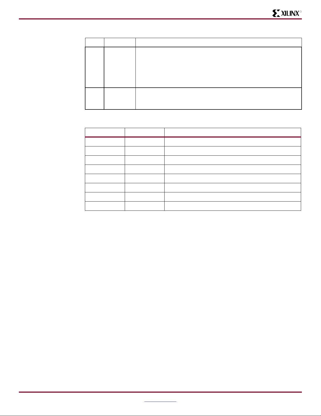
Configuring the OPB IIC Core
Figure 8 shows how to specify the values of IIC generics in EDK. To access the dialog box in
the figure, double click on the OPB IIC core in the EDK System Assembly View..
X979_08_012907
Figure 8: Specifying the Values of OPB IIC Generics in EDK
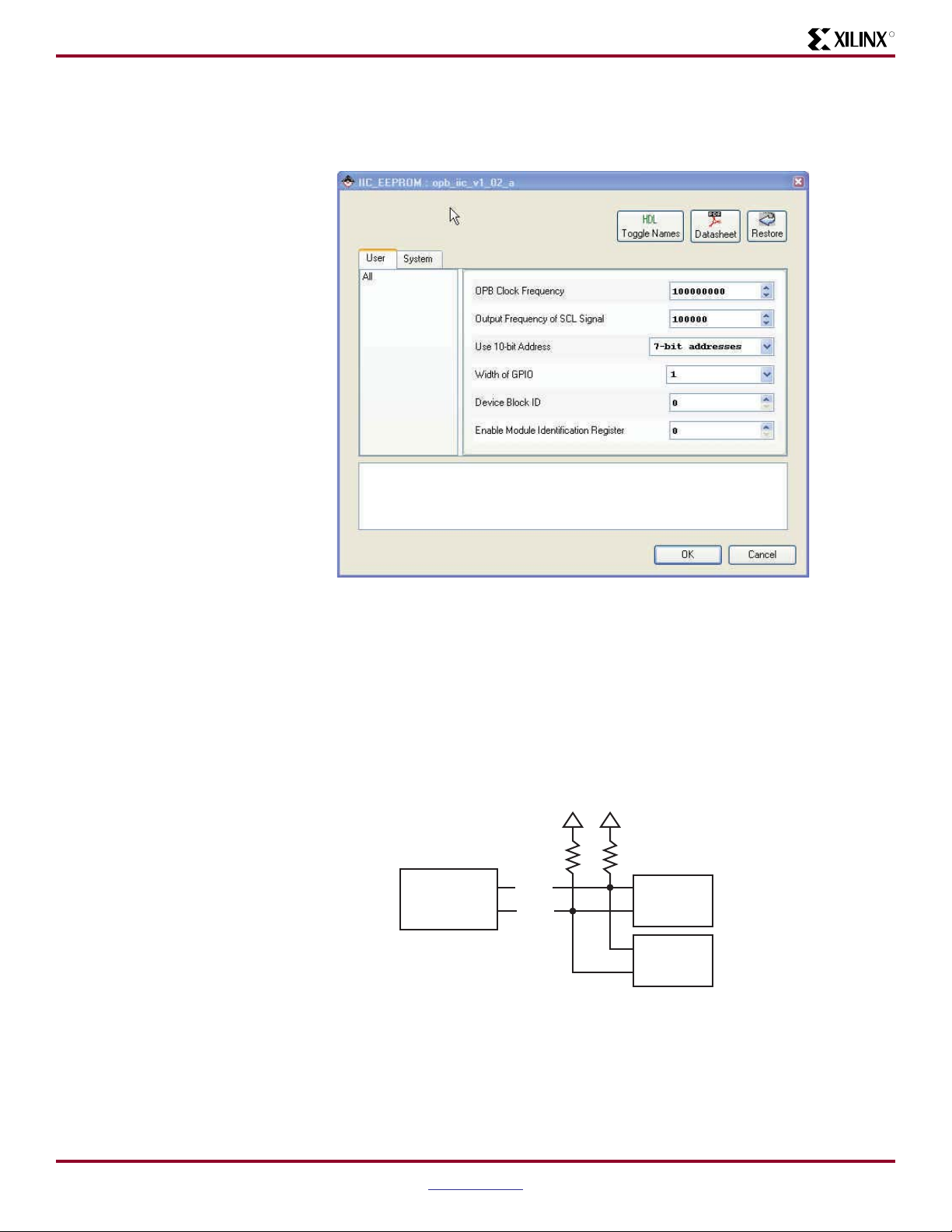
Microchip 24LC04
The Microchip Technology 24LC04B-I/ST with 4-KB EEPROM is provided on the ML403 board
to store non-volatile data. The EEPROM write protect is tied off on the board to disable its
hardware write protect. The IIC bus is extended to the expansion connector to allow additional
devices to be added to the IIC bus.
Figure 9 shows IIC Bus Devices on the ML403.
XC4VSX12
FPGA
SCL
SDA
Microchip
24LC04B
Expansion
Figure 9: ML403 IIC Bus
I/O
Header
X979_09_022307
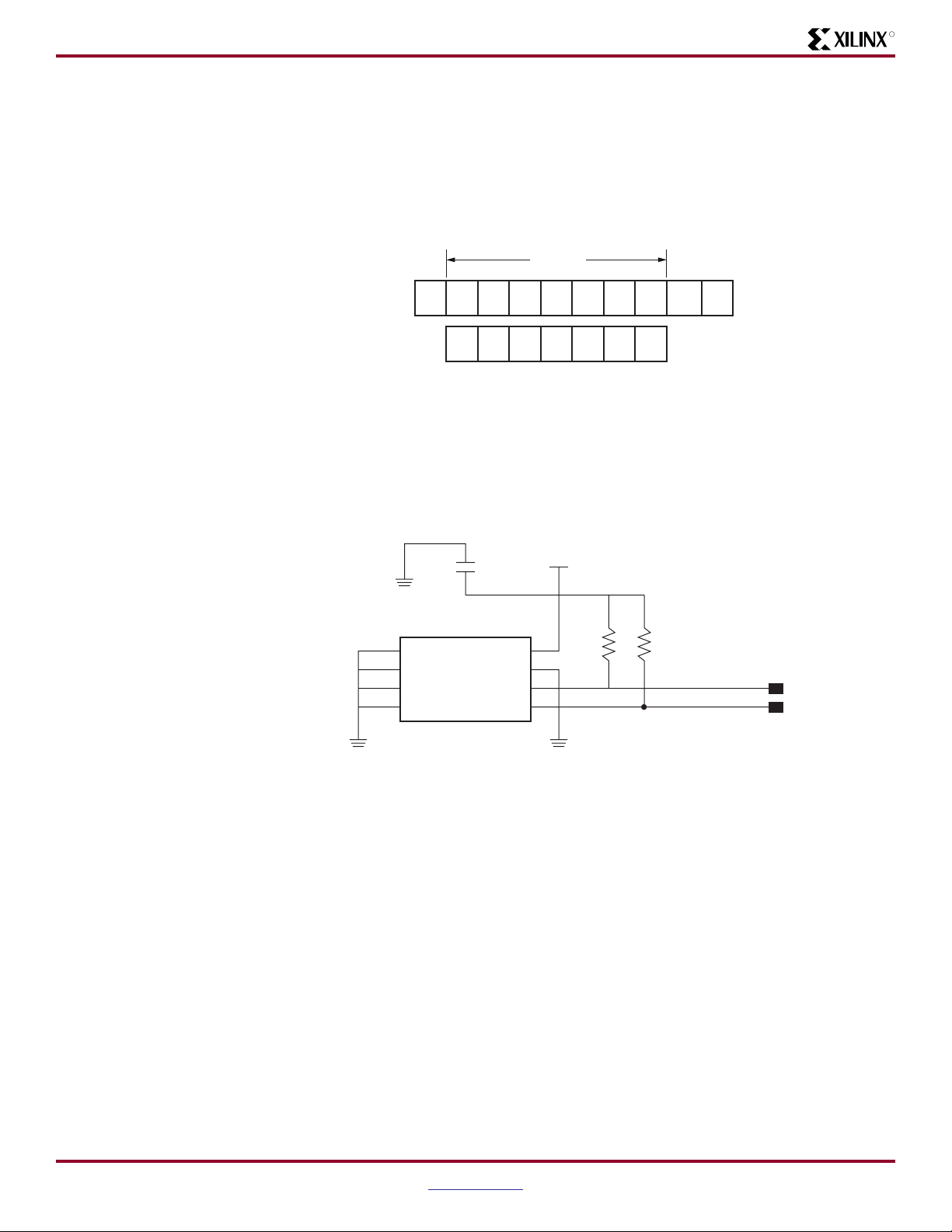
The 24LC04 is organized as two blocks of 256 bytes. It has a page write buffer of up to 16
bytes. The 24LC04 operates as an IIC slave. The 24LC04 accepts a control byte which
contains control code, block select, and Read/Writefields shown inFigure 10. The control code
XAPP979 (v1.0) February 26, 2007 www.xilinx.com 8
Page 9
ML403 Board Information
R
is ‘1010 for read and write operations. The A2, A1 bits are dont cares. The A0 bit is used by the
master device to select which of the two 256-word blocks of memory are accessed. The
24LC04 write transactions are either a byte write or a page write. The page write begins the
same as the byte write but instead of generating a stop condition the master transmits up to 16
data bytes to the 24LC04B. The 24LC04 supports current address, random, and sequential
read operations.
Slave
Address
ML403 Board
Information
S
010A2A1
A01
AR/W
X979_10_012907
Figure 10: 24LC04 Control Byte Allocation
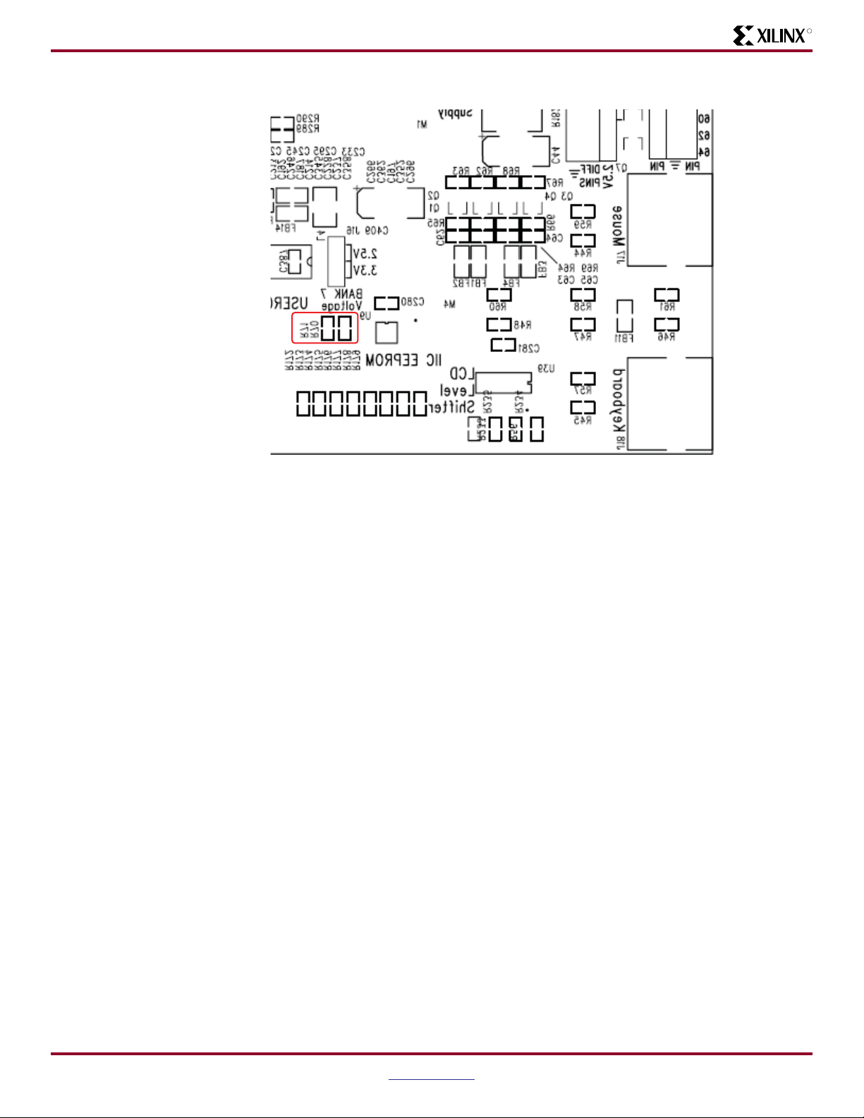
According to the MicroChip 24L024B data sheet, the ML403 board has a low-level output
current (IOL) of 3.0 mA at a VCC of 2.5v. The ML403 boards are shipped in the configuration
shown in Figure 11. The board must be modified for this design to work correctly. Replace the
10K Ohm R70 and R71resistors with 833 or 1K Ohm resistors. See Answer Record 24049 for
additional information.
24LC04B - I / ST
1
A0
2
A1
3
A2
4
A3
C280
0.1 µF
TSSOPSU9
VCC
WP
SCL
SDA
VCC2V5
R70
8
10k
7
6
5
2
2
R71
10k
1
1
IIC_SCL
IIC_SDA
X979_11_022307
Figure 11: ML40x Schematic for IIC Connections
XAPP979 (v1.0) February 26, 2007 www.xilinx.com 9
Page 10
ML403 Board Information
R
The resistors are located on the board as shown in Figure 12.
Figure 12: ML40x Resistors
X979_12_022307
XAPP979 (v1.0) February 26, 2007 www.xilinx.com 10
Page 11

ML403 Board Information
2
If additional IIC devices are connected to the bus via the expansion header as shown in
Figure 13, insert additional pull-up resistors on the external signals connected at pins 31 and
32. The resistor values are dependent on the voltage.
HDR 1 X 32
1
2
3
4
5
6
7
8
9
10
11
12
13
14
15
16
17
18
19
20
21
22
23
24
25
26
27
28
29
30
31
32
J3
NC
NC
FPGA_PROM_CPLD_TMS
FPGA_PROM_CPLD_TCK
EXPANSION_TDO
CPLD_TDO
GPIO_LED_N
GPIO_SW_N
GPIO_LED_C
GPIO_SW_C
GPIO_LED_W
GPIO_SW_W
GPIO_LED_S
GPIO_SW_S
GPIO_LED_E
GPIO_SW_E
GPIO_LED_0
GPIO_LED_1
GPIO_LED_2
GPIO_LED_3
NC
NC
External pullups
connect here
VCC2V5
Level
Translation
MOSFETs
Internal pullups
connect here
IIC_SCL
IIC_SDA
X979_13_01
R
Figure 13: Expansion Header
XAPP979 (v1.0) February 26, 2007 www.xilinx.com 11
Page 12

ML403 Board Information
R
Figure 14 shows the FPGA pins driving the IIC Bus.
IO_L8N_GC_LC_3_C12
IO_L8P_GC_LC_3_C13
IO_L7N_GC_LC_3_A17
IO_L7P_GC_LC_3_B17
IO_L6N_GC_LC_3_B10
IO_L6P_GC_LC_3_A10
IO_L5N_GC_LC_3_A15
IO_L5P_GC_LC_3_A16
IO_L4N_GC_VREF_LC_3_B12
IO_L4P_GC_LC_3_B13
IO_L3N_GC_LC_3_C14
IO_L3P_GC_LC_3_C15
IO_L2N_GC_VRP_LC_3_A11
IO_L2P_GC_VRN_LC_3_A12
IO_L1P_GC_CC_LC_3_B14
IO_L1P_GC_CC_LC_3_B15
FPGA_BANK3
2.5 VCC0
C12
C13
A17
B17
B10
A10
A15
A16
B12
B13
C14
C15
A11
A12
B14
B15
SMA_DIFF_CLK_IN_N
SMA_DIFF_CLK_IN_P
IIC_SCL
IIC_SDA
DDR_CLK1_N
DDR_CLK1_P
DDR_A13
DDR_BA1
DDR_BA0
DDR_CLK_P
MOUSE_DATA
PHY_TXCLK
GPIO_LED_2
GPIO_LED_3
MOUSE_CLK
PHY_RXC_RXCLK
X979_14_012907
Figure 14: FPGA IIC Pins
TotalPhase Aardvark Adapter
In the reference design, the OPB IIC in the XC4VFX12 on the ML403 board interfaces to the IIC
in the Aardvark Adapter. The Aardvark IIC/SPI Embedded Systems interface is a multifunctional host adapter. The Aardvark Control Center software interacts with the Aardvark
Adapter. The Control Center controls the functionality of the Aardvark Adapter. It uses the
AardvarkIIC/SPI Software API. the AardvarkAdapter has six functional modes.The IIC-related
modes are the IIC + SPI and IIC Bus Monitoring modes.
The Aardvark must be configured for use before the Aardvark Control Center software can be
used to send and receive messages. Configuring the Aardvark Adapter binds the instance of
the application with the available unit until the adapter is disconnected or the application is
terminated.
The Configure Aardvark Adapter window is organized into two major sections: list of available
adapters connected to the computer and list of the six operational modes. The main application
window is divided into two sections. The top section contains the modules used with the
AardvarkAdapter.The bottom section contains the transaction log which tracksall transactions
that the Aardvark sends or receives. The transaction log contains the time, read or write
transaction, master or slave, bit rate, address, number of bytes, and data.
XAPP979 (v1.0) February 26, 2007 www.xilinx.com 12
Page 13

ML403 Board Information
R
Figure 15 shows the Aardvark Control Center GUI.
X979_15_012907
Figure 15: Aardvark Control Center
Interfacing to the OPB IIC on the ML403 Board to the Aardvark Adapter
Figure 16 shows the principle interface blocks when transferring data between the OPB IIC in
the XC4VFX12 on the ML403 board and the IIC in the Aardvark Adapter.
ML403 - XCVFX12
DDR
PC
PPC
BRAM
OPB IIC
Aardvark
Adaptor
USB
X979_16_012907
Figure 16: Interfacing ML403 Board OPB IIC with the Aardvark Adapter
Executing the Reference System using the Pre-Built Bitstream and the Compiled Software Applications
To execute the system using files inside the ml403_ppc_opb_IIC/ready_for_download
directory, follow these steps:
1. Change to the ml403_ppc_opb_IIC/ready_for_download directory.
2. Use iMPACT to download the bitstream by using the following:
impact -batch xapp.cmd
XAPP979 (v1.0) February 26, 2007 www.xilinx.com 13
Page 14

ML403 Board Information
R
3. Invoke XMD and connect to the MicroBlaze processor by the following command:
xmd -opt xapp.opt
4. Download the executable by the following command
dow <path>/executable.elf
Executing the Reference System from EDK
To execute the system using EDK, follow these steps:
1. Open system.xmp inside EDK.
2. Use Hardware → Generate Bitstream to generate a bitstream
3. Download the bitstream to the board using Device Configuration → Download
Bitstream.
4. Invoke XMD with Debug Launch XMD.
5. Download the executable by the following command.
dow <path>/executable.elf
Verifying the Reference Design with Xilinx Microprocessor Debugger
After downloading the bitstream file, issue the following XMD commands to verify that the
ML403 reference design is set up correctly.
mrd 0x42600100 8
The expected value of the control register after a reset, located at 0x42600100 is 0x00000000.
The expected value of the status register, located at 0x42600104, is 0x000000C0. The reset
values of the Transmit and Receive FIFO registers are indeterminate. The reset values of the
Transmit and Receive FIFO Occupancy and the Address registers is 0.
Except for the Status, , Receive FIFO, and Transmit and Receive Occupancy registers, all
registers are writeable.
mwr 0x42600100 0xFFFFFFFF
mrd 0x42600100 1
Using XMD commands, verify that the OPB IIC registers can be writtenand read as defined in
Tables 2-5.
Software Projects
The reference system contains the following software projects. In each software project
directory, there is a src sub-directory for the source code. The connections in Figure 9 are
used for the eeprom, low_level_eeprom, dynamic_eeprom, and low_level_dynamic_eeprom
projects. These projects interface to the 24LC04. The connections in Figure 3 are used for the
mult_master and repeated_start project. These projects interface to the IIC Bus via the
Aardvark Adapter.
Projects interfacing to Microchip 24LC04
eeprom: This project transmits and receives data using the high level (L1) software driver. The
OPB IIC is the master and the 24LC04 is configured as the slave. The OPB IIC master writes
data into the 24LC04 and reads it back.
low_level_eeprom: This project transmits and receives data using the low level (L0) software
driver. The OPB IIC is the master and the 24LC04 is configured as the slave. The OPB IIC
master writes data into the 24LC04 and reads it back. This is a polled mode example.
dynamic_eeprom: This project transmits and receives data using the high level (L1) software
driver. The OPB IIC is the master and the 24LC04 is configured as the slave. The OPB IIC
master writes data into the 24LC04 and reads it back.
XAPP979 (v1.0) February 26, 2007 www.xilinx.com 14
Page 15

ML403 Board Information
R
low_level_dynamic_eeprom:This project transmits and receives data using the lowlevel(L0)
softwaredriver.The OPB IIC is the master and the 24LC04 is configured as the slave.The OPB
IIC master writes data into the 24LC04 and reads it back. This is a polled mode example.c
Projects interfacing to Aardvark Adapter
multi_master: This project transmits and receives data using the high level (L1) software
driver. The OPB IIC is an IIC master and the IIC in the Aardvark is a master. The Microchip
24LC04B is configured as a IIC slave.The WP pin of the 24LCO4 is hardwired to ground on the
ML403. The interrupt mode is used. The IIC master in the Aardvark Adapter writes the data to
the MicroChip 24LC04B with the No Stop option enabled. Any attempts to write data from the
OPB IIC master results in a Bus Busy status. The Aardvark Adapter releases the bus by
executing the FREE BUS command. When the bus is free, the OPB IIC master initiates a bus
transaction.
repeated_start: This project transmits and receives the data using the high level (L1) driver.
The IIC devices on the ML300/ML310/ML410 boards do not support the repeated start option.
The ML403 OPB IIC is configured as a master and the Aardvark Adapter IIC is configured as a
IIC slave. The OPB IIC writes the data to the Aardvark IIC in multiple transactions with the
repeated start option enabled. The external IIC device slave address is a 7 bit address defined
by SLAVE_ADDRESS. The number of bytes sent and received is defined by SEND_COUNT
and RECEIVE_COUNT.
Figure 17 shows the repeated start example.
Specify 0x70 as the Address. The SPI Control is not used. The transaction log shows 16 write
and 16 read transactions at address 70.
X979_17_012907
Figure 17: Repeated Start Example
slave: This project transmits and receives the data using the high level(L1) driver.The ML403
OPB IIC is configured as a slave and the Aardvark Adapter IIC is configured as a IIC master.
The Aardvark Adapter IIC writes the data in test_data to the OPB IIC and reads it back.
XAPP979 (v1.0) February 26, 2007 www.xilinx.com 15
Page 16

Running the Applications
R
Figure 18 shows the slave example. The message is in transmit.txt, and is the sentence "Lester
was here.". The transaction log matches the message. The address is 0x70. Click Master
Write to generate the transaction.
Running the
Applications
Figure 18: Slave Example
X979 18 012907
In XPS, select the Applications tab under the Project Information Area to view the Software
Project.
Figure 19 shows the structure of the dynamic_eeprom project. Make the dynamic_eeprom
project active and the remaining software projects inactive.
X979_19_012907
Figure 19: Selecting the eeprom Software Project
XAPP979 (v1.0) February 26, 2007 www.xilinx.com 16
Page 17

Running the Applications
R
Select dynamic_eeprom and right click to build the project. If more than one software project
is used, make the unused software projects inactive.
Connect a serial cable to the RS232C porton the ML403 board. Startup a HyperTerminal. Set
Bits per second to 9600, Data bits to 8, Parity to None, and Flow Control to None, as shown in
Figure 20.
X979_20_012907
Figure 20: HyperTerminal Parameters
From XPS, start XMD and enter rst. Invoke GDB and select Run to start the application as
showninFigure 21. The eeprom.c codewritten for the ML403 shown in the figure runs without
any modifications on this reference system.
X979_21_012907
Figure 21: Running dynamic_eeprom in GDB
XAPP979 (v1.0) February 26, 2007 www.xilinx.com 17
Page 18
Using ChipScope with OPB IIC
R
Using
ChipScope with
OPB IIC
To facilitatethe use of ChipScope to analyze OPB IIC hardware,the iic.cdc file is included in
the ml403_ppc_opb_iic/chipscope directory. The iic.cdc is used to insert a
ChipScope ILA core into the opb_iic core. The following steps are used to insert a core and
analyze OPB IIC problems with ChipScope.
1. Invoke XPS. Run Hardware → Generate Netlist.
2. In the iic.cdc file, change the path <design_directory> name to the directoryin which
the design files are installed. Three paths need to be changed.
3. Run Start → Programs → ChipScope Pro → ChipScope Inserter
4. From ChipScope Inserter, run File → Open Project ii.cdc. Figure 22 shows the ChipScope
Inserter setup GUI.
Figure 22: ChipScope Inserter Setup
X979_22_012907
XAPP979 (v1.0) February 26, 2007 www.xilinx.com 18
Page 19

Using ChipScope with OPB IIC
5. Figure 23 shows the GUI for making net connections. Click Next to move to the Modify
Connections window. If there are any red data or trigger signals, correct them. The Filter
Pattern can be used to find net(s). As an example of using the Filter Pattern, enter intr in the
dialog box to locate interrupt signals. In the Net Selections area, select either Clock, Trigger,
or Data Signals. Select the net and click Make Connections.
R
X979_23_012907
Figure 23: Making Net Connections in ChipScope Inserter
7. Click Insert Core to insert the core into iic_eeprom_wrapper.ngo. In the
ml403_ppc_opb_IIC/implementation directory, copy iic_eeprom_wrapper.ngo to
iic_eeprom_wrapper.ngc.
8. In XPS, run Hardware → Generate Bitstream and Device Configuration → Download
Bitstream. Do not rerun Hardware → Generate Netlist, as this overwrites the
implementation/iic_eeprom_wrapper.ngc produced by the step above.Verifythat the
file size of the opb_iic_wrapper.ngc with the inserted core is significantly larger than the
original version.
9. Invoke ChipScope Pro Core Analyzer by selecting
Start → Programs → ChipScope Pro → ChipScope Pro Analyzer
Click on the JTAG chain icon located at the top left of Analyzer GUI. Verify that the message in
the transcript window indicates that an ChipScope ICON is found.
10. The ChipScope Analyzer waveform viewer displays signals namedDATA*. To replace the
DATA* signal names with the signal names specified in ChipScope Inserter, select File →
Import and enter iic.cdc in the dialog box.
XAPP979 (v1.0) February 26, 2007 www.xilinx.com 19
Page 20

Using ChipScope with OPB IIC
The waveform viewer is more readable when buses rather than discrete signals are displayed.
The Reverse Bus Order operation below Add to Bus in the figure can be useful in analyzing
ChipScope results.
R
X979_24_022307
Figure 24: Setting Up the Chipscope Trigger
11. Set the trigger in the Trigger Setup window.The trigger used depends on the problem being
debugged.Change the Windows to N samples toa setting of 100. Arm the triggerby selecting
Trigger Setup → Arm, or clicking on the Arm icon.
As shown in Figure 24, the trigger setup is to trigger when gen_start is High.
12. Run XMD and/or GDB to activate the trigger patterns which cause ChipScope to display
meaningful output.
XAPP979 (v1.0) February 26, 2007 www.xilinx.com 20
Page 21

Linux Kernel
R
13. ChipScope results are analyzed in the waveform window as shown in Figure 25. The
waveforms may be easier to read if the discrete signals are removedafter they are renamed. To
share the results with remote colleagues, save the results in the waveform window as a Value
Change Dump (vcd) file. The vcd files can be translated and viewed in most simulators. The
vcd2wlf translator in Modeltech reads a vcd file and generates a wlf file for viewing in the
Modeltech waveform viewer. The vcd file can be opened in the Cadence Design System, Inc.
Simvision design tool by selecting File → Open Database.
X979_25_012907
Figure 25: ChipScope Analyzer Results
Linux Kernel New users of MontaVista Linux should read XAPP 765 Getting Started with EDK and Monta
Vista Linux. The steps to build and boot a Linux kernel are given below. Steps 1-3, 7, 8 are run
on a Linux machine with MontaVista Professional Edition© installed.
1. Add /opt/montavista/pro/host/bin and
/opt/montavista/pro/devkit/ppc/405/bin
to $PATH.
2. Change to the ml403_IIC/linux directory.
3. Run
tar cf - -C /opt/montavista/pro/devkit/lsp/xilinx-ml300ppc_405/linux-2.4.20_mvl31/ . tar xf -
4. To generate the Linux LSP in XPS, enter Software → Software Platform Settings.
Select Kernel and Operating Systems, then select linux_mvl31 v1.00.c.
XAPP979 (v1.0) February 26, 2007 www.xilinx.com 21
Page 22

Linux Kernel
R
5. Under OS and Libraries, set the entries as shown in Figure 26.
X979_26_012907
Figure 26: BSP Settings
Verify that the target directory is the same as the directory containing the Linux source.
XAPP979 (v1.0) February 26, 2007 www.xilinx.com 22
Page 23

Linux Kernel
R
6. Click Connect_Periphs and add the OPB_INTC, OPB_SYSACE, OPB_IIC, OPB_SPI,
OPB_IIC, and OPB 16550 peripherals, using the instance names shown in Figure 27.
X979_27_012907
Figure 27: Connected Peripherals
Click OK.
7. Select Software → Generate Libraries and BSPs to generate the LSP in
ml403_ppc_opb_iic/linux.
8. From ml403_ppc_opb_iic/linux, run
patch_nobspgen.
9. The ml403_ppc_opb_iic/linux/.config is used to define the contents of the Linux
kernel. Run
make oldconfig
An alternative is to enter make menuconfig and generate a new .config using the following
options.
• Select General Setup
• Enable IIC. Disable PS/2 keyboard. Change to /dev/ram for booting from ramdisk.
• Select Input Core Support. Disable all.
• Select Character Devices. Disable Virtual. Leave Serial enabled. Disable Xilinx GPIO and
Touchscreen.
10. Run make clean dep zImage.initrd. Verifythat the zImage.initrd.elf fileis in
the ml403_ppc_opb_iic/linux/arch/ppc/boot/images directory.
11. Invoke Impact and download implementation/download.bit to XC4VFX12. Either
select Device Configuration → Download Bitstream from XPS or run the following
XAPP979 (v1.0) February 26, 2007 www.xilinx.com 23
Page 24

Simulation
command from the command prompt:
impact -batch etc/download.cmd
12. Invoke XMD. From the ml403_ppc_opb_iic/linux directory, enter the following
commands in the XMD window.
rst
dow arch/ppc/boot/images/zImage.initrd.elf
con
13. View the output in the HyperTerminal window. Login as root. Enter cd / and ls -l to
view the contents of the mounted Linux partition.
14. An alternative to downloading the Linux kernel executable is to load it into CompactFlash.
The file used uses an ace file extension. To generate an ace file, run the command below
from the ml403_ppc_opb_iic directory.
xmd -tcl /genace.tcl -jprog -hw ./implementation/system.bit -ace
./implementation/ace_system_hw.ace -board ML403
Copy the ace file to a 64-512 MB CompactFlash (CF) card in a CompactFlash reader/writer.
Removethe CFcard from the CF reader/writer and insert itinto the CompactFlash slot (J22) on
the ML403 board. Power up the board.
Simulation The ml403_ppc_opb_iic/simulation directory contains waveformlog file, opb_iic.wlf,for
IIC transactions discussed in this section.
R
The opb_iic.wlf files are easily loaded into the Modeltech simulator using the File → Open
command, specifying the *.wlf file type.
The OPB IIC core has two Finite State Machine (FSM). The clock FSM has IDLE, START,
SCL_LOW_EDGE,SCL_LOW,SCL_HIGH_EDGE,SCL_HIGH,STOP_WAITstates.The main
FSM has IDLE, HEADER, ACK_HEADER, RCV_DATA, XMIT_DATA, ACK_DATA, and
WAIT_ACK states.
Figure 28 shows the two OPB IIC cores in the simulation. The simulation is a Bus Functional
Model simulatation of two OPB IIC cores. The IIC cores with addresses 20 and AA are
designated iic_20 and iic_AA, with C_BASEADDR of 0xE0000000 and 0xE1000000,
respectively. Both cores connect to SCL and SDA. The stimuli is provided by writing the OPB
IIC registers.
As an example
write cr 41
enablesthe OPB IIC and sets the General Call enable. The address determines which OPB IIC
is the target of the write, with 0xE0000100 for iic_20 and 0xE1000100 for iic_AA. It may be
useful to consult the register map in Table 2 and the control (Table 3), status (Table 4), and
interrupt status register (Table 5) definitions.
XAPP979 (v1.0) February 26, 2007 www.xilinx.com 24
Page 25

Simulation
R
In most cases, after data is transmitted, the test waits for an interrupt from the OPB IIC.
BFM
IIC_20
Base Address
0xE0000000
SCL
SDA
IIC_AA
Base Address
0xE1000000
X979_28_012907
Figure 28: OPB IIC Simulation
Internal signal names used in the OPB IIC core are provided in Table 6.
Table 6: Internal Signals in OPB IIC
Signal Name Functionality
Txak Transmit acknowledge
Gc_en General call address enbale
Ro_prev Receive overrun prevent
Dtre Data transmit register empty
Msms Master/Slave select
Dtr(7:0) Data Transmit Register
Adr(7:0) IIC Slave Address Register
Ten_adr(7:5) 10-bit Slave Address Register
Bb Bus Busy
Aas Addressed as slave
Al Arbitration lost
Srw Slave read/write
Abgc Addressed by general call
Data_iic(7:0) IIC data for microprocessor
New_rcv_data New data received on IIC bus
Tx_under_prev Transmit FIFO Empty IRQs
slave_sda SDA value when slave
master_sda SDA value when master
sm_stop Stop condition needs to be generated
rsta_tx_under_prev Repeated start Tx underflow prevent
XAPP979 (v1.0) February 26, 2007 www.xilinx.com 25
Page 26
Simulation
R
The simulation runs for 2000 ns as shown in Figure 29. There are 3 sections in the simulation,
shown in the following figures.
X979_29_022307
Figure 29: Complete Simulation
XAPP979 (v1.0) February 26, 2007 www.xilinx.com 26
Page 27
Simulation
R
In the first test, which is shown in Figure 30, the OPB IIC registers are read to verify the correct
reset values. The interrupt registers are written and read. This occurs from 0 - 10 s. Following
this, an arbitration test is run. IIC_AA is initially the bus master, with the write CR_AA 0x0d.
X979_30_022307
Figure 30: Arbitrartion Lost Test Simulation
XAPP979 (v1.0) February 26, 2007 www.xilinx.com 27
Page 28

Simulation
R
Figure 31 provides the Arbitration Lost test code. This pseudo-code can be tracked in the
simulation.
wri te ADR_20 0x20
wri te CR_20 40
wri te CR_AA 0x01
wri te ADR_AA AA
wri te IER_AA 0x04
wri te RC_FIFO_PIRQ_20 0x0
wri te DT R_AA 0x0
wri te CR_AA 0x0D -- Enab les AA as master (5.9us)
wri te IPIER_20 0x01
wri te DT R_20 AA
wri te CR_20 0x0D -- E nables 20 as master
wait_for_intr (30)
read IPISR 0x D 3 -- Arbitration lost (260 us)
wri te CR_20 0x01 -- Clears inter ru pt
X979_31_012907
Figure 31: Arbitration Lost Test Code
XAPP979 (v1.0) February 26, 2007 www.xilinx.com 28
Page 29

Simulation
R
The second test, shown in Figure 32, runs from 575 s to 790 s., Ths master, AA, receives 3C
and 55 from 20. The following stimuli / results is seen in the opb_iic.wlf file.
Figure 32: Simulation with iic_AA as Master
X979_32_022307
XAPP979 (v1.0) February 26, 2007 www.xilinx.com 29
Page 30

Simulation
R
Figure 33 provides the test code used in the simulation with the OPB IIC with the AA address
as the master.
wri te CR_20 0x40 -- GC, En
wri te ADR_20 0x20 - Sets address as 0x2 0
wri te CR_AA 0x01 - En ab le
write ADR_AA 0xAA
wri te RC_FIFO _P IRQ_AA 0x0
wri te IER_AA 0x04 -- Enable DTRE interrupt
wri te RC_FIFO _P IRQ 0x01 (473 us)
wri te DT R_20 0x3C
wri te DT R_20 0x55
wri te DT R_AA 0x0 -- G eneral Call
wri te CR_AA 0x0D -- RSTA, Tx AK, TX, M SMS, Enable
wait_for_intr
read SR_AA 0x C4 -- TFE, RFE, BB
read ISR_ AA 0xD4 -- TFHE, DTRE
wri te CR_AA 0x35 RSTA, MS, EN (547 us)
wri te DT R_AA 0x21
wri te DT R_AA 0xFF
wri te IER_AA 0x08
wait_for_intr -- wa iting for DRR_AA full
read SR_AA 0x 0C -- SRW , BB (678 us)
wri te CR_AA 0x37 -- Clear FIFO
wri te CR_AA 0x35
read DRR_AA 0x3C
wri te ISR_A A 0 x C*
wri te DT R_AA 0x21
wait_for_intr
read SR_AA 0x 8C
read ISR_ AA 0xCA -- TXER, DF F F u ll
wri te CR_AA 0x41
read DRR_AA 0x55 (787 us)
wri te ISR_A A 0 x C8
wri te IRE_AA 0x10 -- Enable Bus is no t Busy
wait_for_intr
X979_33_012907
Figure 33: Test code with iic_AA as Master
XAPP979 (v1.0) February 26, 2007 www.xilinx.com 30
Page 31

Simulation
R
Figure 34 shows the third test shown in opb_iic.wlf, run from 800 - 2000 us. IIC_20 is the
master writing to IIC_AA, which is a 10-bit slave.
Figure 34: Simulation with iic_AA as Master
X979_34_012907
XAPP979 (v1.0) February 26, 2007 www.xilinx.com 31
Page 32

Simulation
R
Figure 35 provides the test code for simulation with IIC_AA as master.
write DTR_20 0xF2
write DTR_20 0xD5
read TX_FIFO_OCY 0x01
write CR_20 0x0D -- Tx, MS, En
write RC_FIFO_PIRQ 0x01
write IER_AA 0x20 -- Enable AAS
wait_for_intr
read SR_AA C6 -- TFE, RFE, BB, AAS (893 us)
write DTR_AA 0x11
write DTR_AA 0x22
write IER_AA 0x47
read ISR_AA 0xA0 -- TFE, FFF
read SR_20 C4 -- TFE, RFE, BB
write IER_20 0x3F -- Enable DTRE
wait_for_intr -- DTRE occurs, D5 sent, and
throttle for 1500 ns
write DTR_20 0xC3 (928 us)
write DTR_AA AA
wait_for_intr -- DTRE occurs, C3, AA sent, and
throttle for 1500 ns
write CR 0x25 -- RSTA, Master Receive, MS, Enable
write DTR_20 0xF3
read DRR_20 0xC3
wait_for_intr -- DRR full occurred, repeated start,
F3 sent on bus
read ISR-20 0xCC -- RFF (1130 us)
read DRR_20 0x11 -- No Ack Master Receive
write CR_20 0x15
write ISR_20 0xCC
write IER_20 0x3B
wait_for_intr -- DRR full, 0x22 received, throttle
for 1500 ns
write DTR_20 0xF2 -- Most significant address
write DTR_20 0xD5 -- Least significant address
write DTR_20 E1
read TX_FIFO_OCY 0x02read SR_AA 0x8E
read DRR_AA 0xAA
read SR_AA 0xCE
write DTR_20 0xD2
write DTR_20 0xC3
write DTR_20 0xB4
read TX_FIFO_OCY_20 0x05
read SR_20 0x0C -- SRW, BB
Figure 35: Test Code for Simulation with iic_20 as Master
write DTR_20 0xA5
write DTR_20 0x96
write DTR_20 0x87
write DTR_20 0x78
write DTR_20 0x60
write DTR_20 0x5A
write DTR_20 0x4B
write DTR_20 0x3C
write DTR_20 0x2D
wrote DTR_20 0x1E
read TX_FIFO_OCY_20 0x0F -- 1207 us
write DTR_20 0x0F
read TX_FIFO_OCY_20 0x0F
read SR_20 0x1C -- TFF, SRW, BB
write DTR_20 0x00
read TX_FIFO_OCY_20 0x0F
read SR_20 0x1C
write DTR_20 0xFF
write RC_FIFO_PIRQ_AA 0x0D
write CR_20 0x2D -- RSTA, TXAK,
MS, EN Starts transmission
read DRR_20 0x22
read ISR_AA 0xEE
write IER_AA 0x08
wait_for_intr -- DRR_55 Full
read DRR_AA 0xE1 -- 1948 us
read DRR_AA 0xD2
read DRR_AA 0xC3
read DRR_AA 0xB4
read DRR_AA 0xA5
read DRR_AA 0x96
read DRR_AA 0x87
read DRR_AA 0x78
read DRR_AA 0x69
read DRR_AA 0x5A
read DRR_AA 0x4B
read DRR_AA 0x3C
read DRR_AA 0x2D
read DRR_AA 0x1E
write CR_20 0x09 -- TxAK, EN
write DTR_20 0x55
X979_35_012907
XAPP979 (v1.0) February 26, 2007 www.xilinx.com 32
Page 33

References
References DS434 OPB IIC Bus Interface (v1.02a)
XAPP765 Getting Started with EDK and MontaVista Linux
ML40x Embedded Development Platform User Guide UG080 (v2.5) May 24, 2006
ChipScope ILA Tools Tutorial
The IIC Bus Specification Version 2.1 January 2000 Philips Semiconductors
R
Revision History
The following table shows the revision history for this document.
Date Version Revision
2/26/07 1.0 Initial Xilinx release.
XAPP979 (v1.0) February 26, 2007 www.xilinx.com 33
 Loading...