

UCC38531
11/97
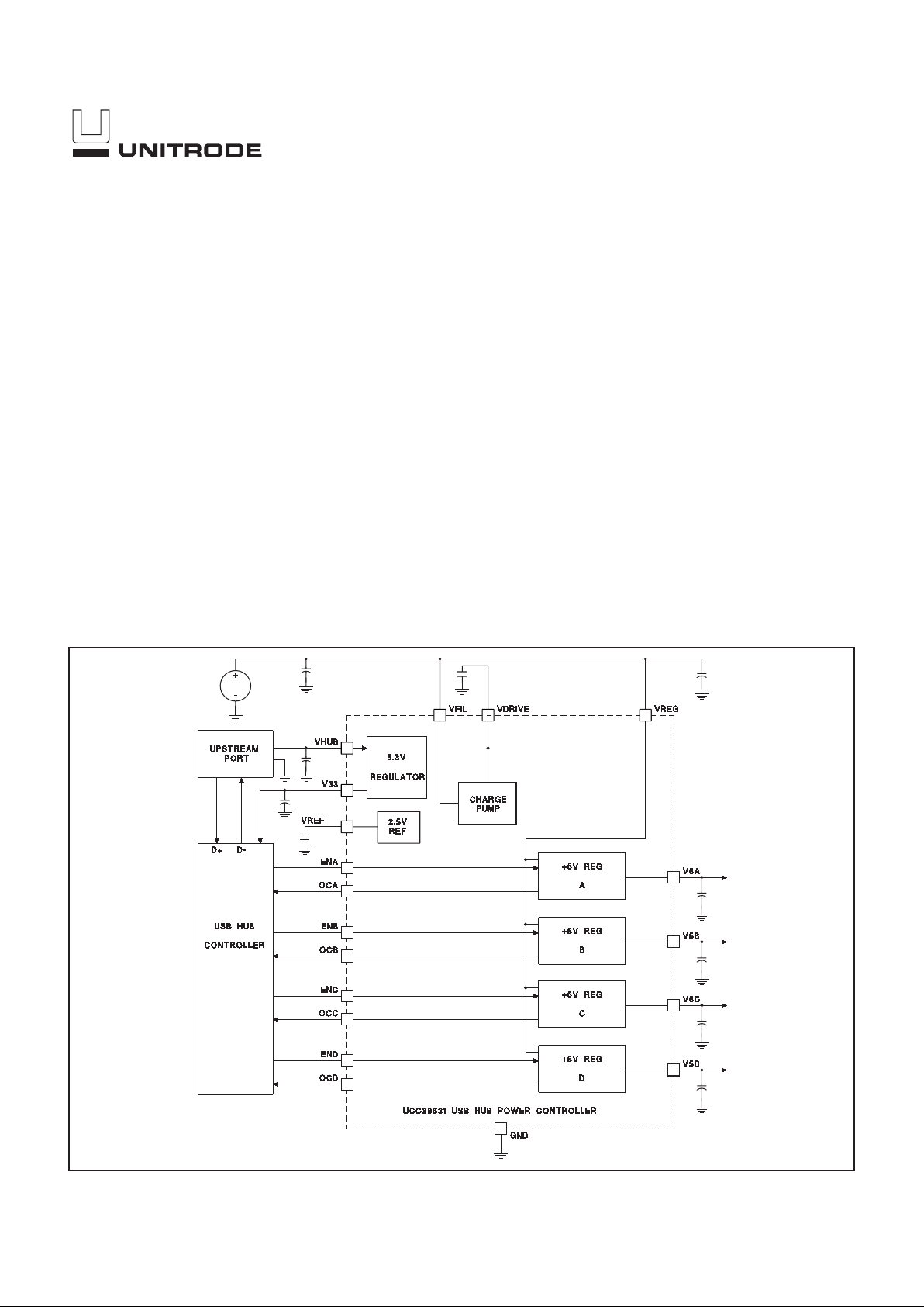
APPLICATION AND BLOCK DIAGRAM
• Fully USB Compliant
• Support Four 5V Peripherals and
One USB 3.3V Controller
• Separate Power Enables
• 500mA Current Limiting per
Channel
• Separate Open Drain Fault
Indicator for Each Channel
• 3.3V Output for USB Controller
• Available in 20 Pin DIP
Universal Serial Bus Power Controller
FEATURES
DESCRIPTION
PRELIMINARY
UDG-97165-1
The UCC38531 Power Controller is designed to provide a self powered
USB hub with a local 3.3V regulated voltage and four 5V regulated voltages for USB ports. Each of the 5V output ports is individually enabled
for optimal por t control. Each port also provides an overcurrent fault signal indicating that the port has exceeded a 500mA current limit. The
3.3V linear regulator is used to power the local USB microcontroller.
This regulator is protected with a 100mA current limit.
The UCC38531 is configured by connecting the VREG to a regulated
5.5V 2A source.
The 20-pin DIP package is protected by internal over-temperature shut-
down mechanism, which disables the outputs should the internal junction temperature exceed 150°C.
2
UCC38531
PARAMETER TEST CONDITIONS MIN TYP MAX UNITS
Input Supply Currents
VHUB Supply Current No External Load on V33 1 3 mA
VFIL Supply Current 13mA
Reference
VREF Voltage Over Temperature 2.35 2.5 2.65 V
Line Regulation VHUB = 4.5V to 9V 3 10 mV
3.3V Regulator
V33 Voltage T
J = 25°C, ILOAD = 10mA 3.2 3.3 3.4 V
0mA to 100mA, 0°C to 125°C, VHUB = 4.5V to 9V 3.165 3.3 3.435 V
Short Circuit Current Limit VHUB = 6V, Output shorted to Ground 100 120 150 mA
5V Regulator
V5A-D Voltage T
J = 25°C, ILOAD = 250mA, VREG = 5.5V 4.85 5 5.15 V
0mA to 500mA, 0°C to 125°C 4.8 5 5.2 V
Short Circuit Current Limit VREG = 5.5V, Output Shorted to Ground 500 600 750 mA
Charge Pump
Quiescent Output Voltage T
J = 25°C, VFIL = 6V, ENA-D = 5V, ENHUB = 5V 11 11.45 12 V
0°C to 125°C, VFIL = 6V 10.5 11.45 12 V
Output Impedance 915kΩ
Enable Inputs
ENA-D Inputs - Guaranteed Low 0.7 V
ENA-D Inputs - Guaranteed High 3 V
Overcurrent Signals
Active Sink Current I
OCX =100
m
A 140 500 mV
ELECTRICAL CHARACTERISTICS Unless otherwise specified, TJ = 0°C to 125°C for the UCC38531. VFIL = 6.5V,
VHUB = 5V. TA =TJ.
ABSOLUTE MAXIMUM RATINGS
VFIL............................................9V
VCON Supply Votage ..............................9V
Logic Inputs (ENA-D)
Maximum Forced Voltage .................–0.3V to 7V
Maximum Forced Current ......................±1mA
V33
Maximum Forced Voltage.........................5V
Maximum Current ...........................200mA
V5A-D
Maximum Voltage...............................9V
Maximum Current ...........................750mA
Storage Temperature ...................−65°C to +150°C
Junction Temperature...................–55°C to +150°C
Lead Temperature (Soldering, 10 sec.).............+300°C
Unless otherwise indicated, voltages are reference to ground.
Pulsed is defined as a less than 10% duty cycle with a maximum
duration of 500
µ
S.Currents are positive into, negative out of the
specified terminal. All voltages are with respect to ground. Consult Packaging Section of Databook for thermal limitations and
considerations of packages.
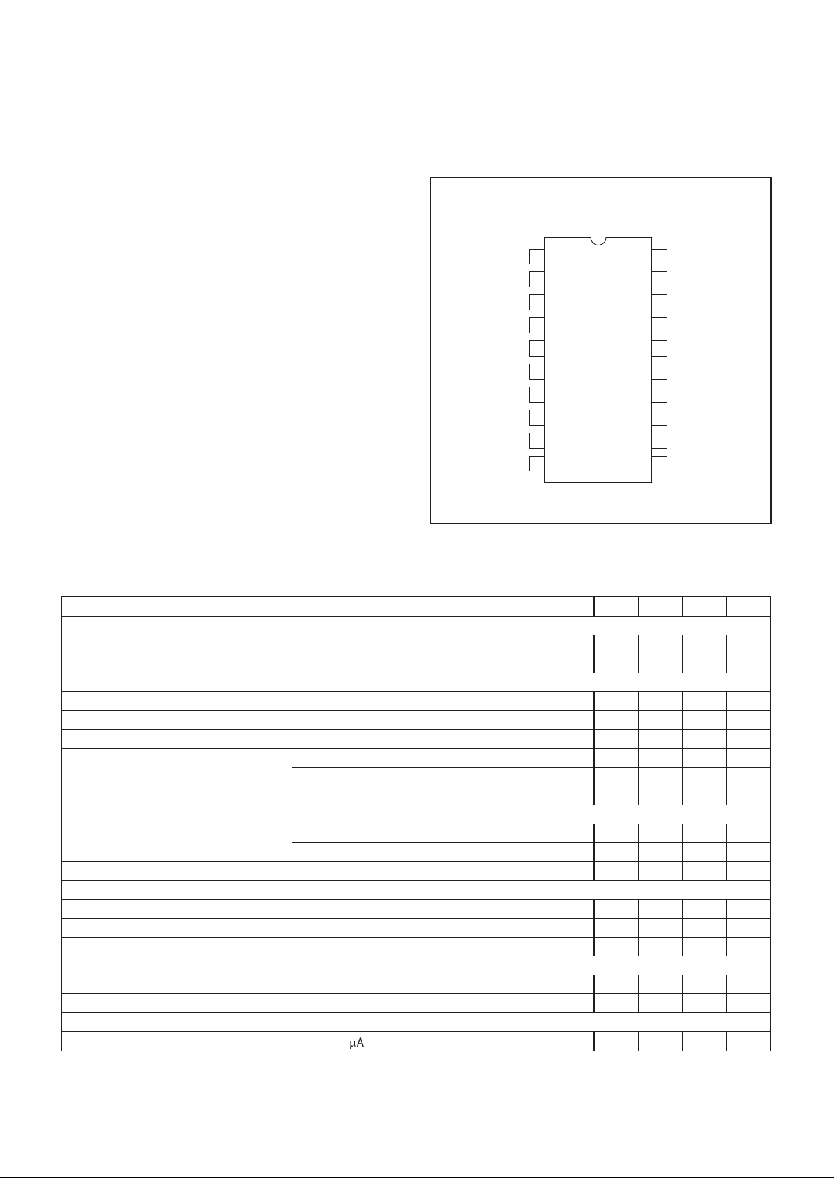
CONNECTION DIAGRAM
OCA
ENA
VSA
V5D
VREG
VDRIVE
OCC
VC5
ENC
VREG
1
2
3
4
5
6
7
8
9
10
20
19
18
17
16
15
14
13
12
11
OCB
GND
OCD
V5B
VREF
VFIL
END
ENB
V33
VHUB
DIP-20 (Top View)
N Package
 Loading...