

3/97
DESCRIPTION
• Transformerless Off-Line
Operation
• Low Voltage Operation to 0.8V
• Ideal for Battery Trickle Charger
Applications
• Current Mode Operation With
100mV Shunt
• Voltage Mode Operation With
Fixed 1.25V Output or Resistor
Adjustable Output
• Efficient BiCMOS Design
• Inherent Short Circuit Protection
The UCC3890 controller is optimized for use as an off-line, low power, low
voltage, regulated current supply, ideally suited for battery trickle charger
applications. The unique circuit topology used in this device can be visualized as two cascaded flyba ck converters; each operating in the discontinuous mode, and both driven from a si ngle external power switch. The
significant benefit of this approach is the ability to charge low voltage batteries in off-line applications with no transformer, and low internal losses.
The control algorithm used by the UCC3890 forces a switch on time inversely pr oportional to t he input line v oltage, whil e the switch off time is
inversely proportional to the output voltage. This action is automatically
controlled by a n i n te r na l fe ed ba c k loo p and reference. The cascaded configuration al lows a large voltage con version ratio with r easonable switch
duty cycle.
While the UCC3890 is ideally suited for control of constant current battery
chargers, provision is also made to operate as a fixed 1.25V regulated
supply, or to use a resistor v o l tage di vi der to obtain output vol tages hi gher
than 1.25V.
UCC1890
UCC2890
UCC3890
Off-Line Battery Charger Circuit
FEATURES
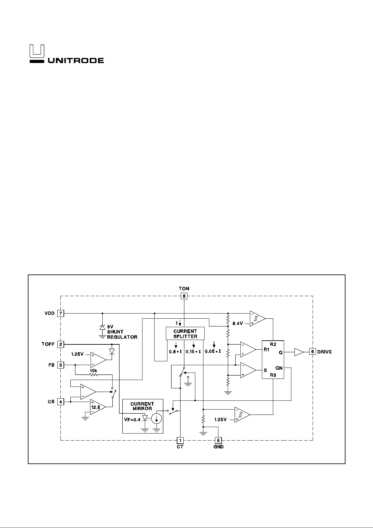
BLOCK DIAGRAM
UDG-96052
Note: This device incorporates patented technology used under license from
Lambda Electronics, Inc.
UCC1890
UCC2890
UCC3890
IDD . . . . . . . . . . . . . . . . . . . . . . . . . . . . . . . . . . . . . . . . . . 7.5mA
Current into TON . . . . . . . . . . . . . . . . . . . . . . . . . . . . . . . 7.5mA
Voltage on V
OUT . . . . . . . . . . . . . . . . . . . . . . . . . . . . . . . . . . . . . . . . . . .
20V
Current into TOFF . . . . . . . . . . . . . . . . . . . . . . . . . . . . . . 250µA
Storage Temperature . . . . . . . . . . . . . . . . . . . –65°C to +150°C
Junction Temperature . . . . . . . . . . . . . . . . . . –55°C to +150°C
Lead Temperature (Soldering, 10 sec.) . . . . . . . . . . . . . +300°C
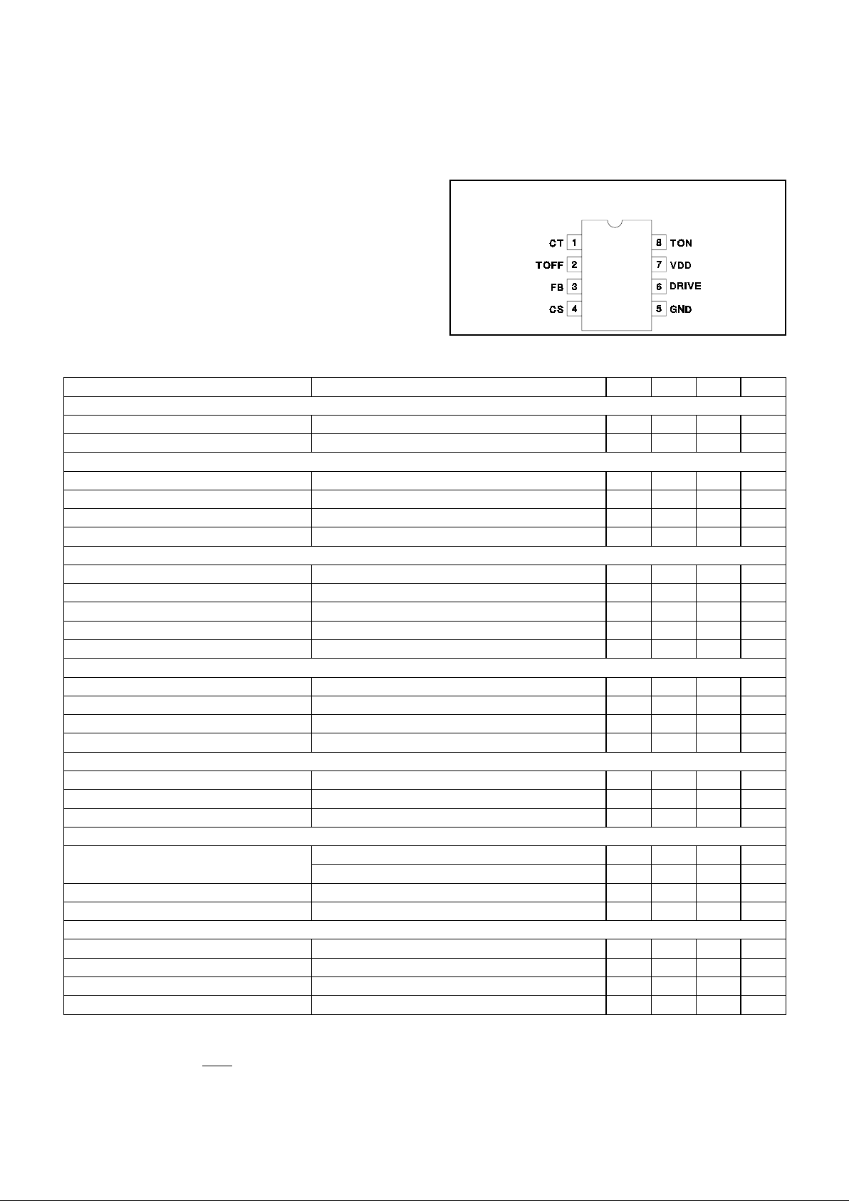
CONNECTION DIAGRAMS
Currents are positive into, negative out of the specified terminal.
Consult Packaging Section of Databook for thermal limitations
and considerations of packages.
ABSOLUTE MAXIMUM RATINGS
PARAMETER TEST CONDITIONS MIN TYP MAX UNITS
General
VDD Zener Voltage I
DD
= 4.75mA,I
TON
= 0mA 8.3 9.0 9.4 V
Minimum Operat in g C urre nt I
TON
IDD = –1mA, F = 150kHz 1.65 2.0 mA
Undervoltage Lockout
Minimum Voltage to Start FB = 0 7.8 8.6 9.2 V
Minimum Voltage after Start FB = 0 5.75 6.3 6.65 V
Hysteresis FB = 0 1.8 2.3 2.6 V
VDD – V
START
FB = 0 0.2 0.4 0.7 V
Oscillator
Amplitude I
TON
= 3mA; I
TOFF
= 50µA; VFB = 0V CT = 100pF 3.1 3.4 3.7 V
CT to DRIVE High Delay Overdrive = 200mV 80 200 ns
CT to DRIVE Low Delay Overdrive = 200mV 50 100 ns
Charge Coefficient I
CT/ITON
I
TON
= 3mA; V
CT
= 3.0V 0.135 0.15 0.165µA/µA
Discharge Coefficent I
CT/ITOFF
I
TOFF
= 50µA; VCT = 3.0V 0.95 1.00 1.05µA/µA
Driver
V
OL
I = 100mA (Note 1) 0.7 1.8 V
V
OH
I = –100mA referred to VDD (Note 1) –2.9 –1.5 V
Rise Time C
L
= 1nF 35 70 ns
Fall Time C
L
= 1nF 30 60 ns
Line Voltage Detection
Minimum I
TON
for Fault 1.0 1.5 2.0 mA
I
TON
Detector Hysteresis 110
µ
A
On Time During Fault 0.5
µ
s
V
OUT
Error Amplifier
Reference Level I
TOFF
= 50µA, ICT = 25µA, TJ = 25°C 1.20 1.25 1.30 V
I
TOFF
= 50µA, ICT = 25µA, Over Temperature 1.15 1.25 1.35 V
Voltage at TOFF I
TOFF
= 50µA 0.3 0.4 0.5 V
Regulation gm I
TOFF
= 50µA (Note 2) 2.0 4.0 7.7 mA/V
Current Sense Amplifier
Gain VCS = 90 – 110mV 11.8 12.5 13.0 V/V
Input Offset Voltage V
CS
= 90 – 110mV –5 0 5 mV
Input Voltage for CS Amplifier Enabled I
TON
= 3mA, Referred to VDD –1.5 –0.8 V
Input Voltage for CS Amplifier Disabled I
TON
= 3mA, Referred to VDD –0.8 –0.3 V
ELECTRICAL CHARACTERISTICS:
Unless otherwise stated, these specifications apply for TA = –55°C to 125°C for
UCC1890, –40°C to 85°C for the UCC2890, and 0°C to 70°C for the UCC3890. No load at DRIVE pin (C
LOAD
= 0), TA = TJ.
DIL-8, SOIC-8 (Top View)
J, N, or D Packages
Note 1: VDD forced to 100mV below VDD Zener Voltage
Note 2: gm is defined as
∆
I
CT
∆
V
FB
for the values of VFB where the error amp is in regulation. The two points used to calculate gm
are for I
CT
at 65% amd 35% of its maximum value.
2
UCC1890
UCC2890
UCC3890
PIN DESCRIPTIONS
CS:
The high side of the current sense shunt is connected to this pi n. Short CS to VDD for voltage feedback
operation.
CT:
Oscillator timing capacitor is connected to this pin.
DRIVE:
Gate drive to external power switch.
FB:
Output of current sense amplifier. This pin can be
used for direct output voltage feedback if the current
sense amp input pin CS is shorted to the VDD pin.
GND:
Ground pin.
TOFF:
Resistor R
OFF
connects from voltage output to
this pin to provide a maximum capacitor discharge current proportional to output voltage.
TON:
Resistor R
ON
connects f rom lin e in put to this pin to
provide capacitor charge current proportional to line voltage. The current in R
ON
also provides power for the 9V
shunt regulator at VDD.
VDD:
Output of 9V shunt regulator.
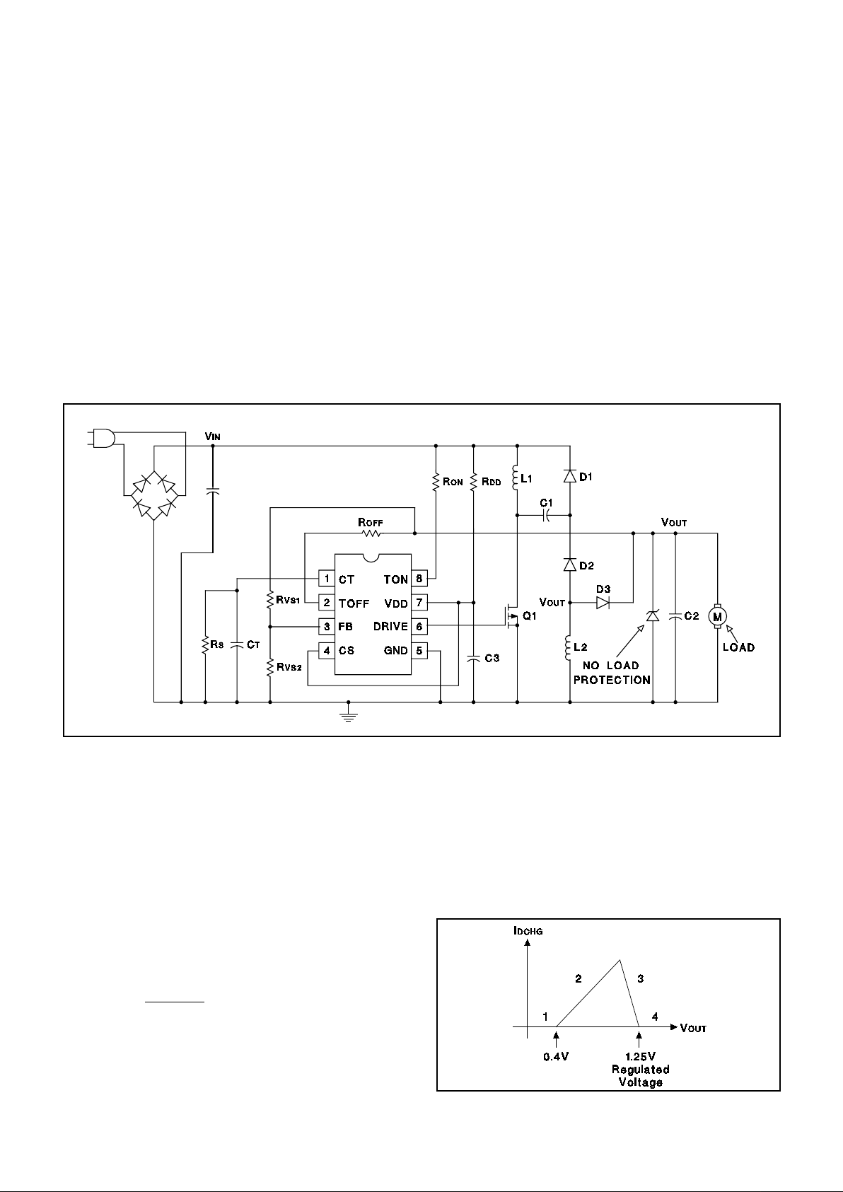
APPLICATION INFORMATION
OPERATION (VOLTAGE OUTPUT)
Figure 1 shows a typical voltage mode application.
When input voltage is first applied, all of the current
through R
DD
and 80% of the current through R
ON,
charge the ext ernal ca paci tor C3 conn ected to VDD. As
the voltage builds on VDD, u ndervoltage lockout holds
the circuit off and the output DRIVE low until VDD
reaches 8.4 V. At this time, DRIV E go es h igh, turning on
the external power switch Q1, and 15% of the current
into TON is directed to the timing capacitor C
T
. The volt-
age at TON is fixed at approximately 11V, so C
T
charges to a fixed threshold with current
I = 0.2 •
V
IN
– 11V
R
ON
Since the input line is much greater than 11V, the
charge current is approximately proportional to the input
line voltage. DRIVE is only high while C
T
is charging, so
the power swi tc h on time i s inver sely pr oportional to l ine
voltage. Thi s provides a constant line voltage-switch on
time product.
At the end of the switc h on time, Q1 i s turned off, and
the 15% of the R
ON
current which was charging CT is
diverted to ground. The power swi tch off time is controlled by discharge of C
T
, which is determined by the outut
voltage as described here:
Figure 1. Typical Voltage Mode Application
UDG-96053
UDG-96054
3

UCC1890
UCC2890
UCC3890
1. When V
OUT
= 0, the off time is infinite. This feature
provides inherent short circuit protection. However,
to ensure output voltage startup when the output is
not a short, a high value resistor, R
S,
is placed in
parallel with C
T
to establish a minimum switching
frequency.
2. As V
OUT
rises above approximately 0.4V, I
DCHG
is
set by R
OFF
, and is defined by
I
DCHG
=
V
OUT
– 0.4V
R
OFF
As V
OUT
increases, I
DCHG
increases resulting in the
reduction o f off time. The frequency of operation increases and V
OUT
rises quickly to its regulated
value.
3. In this regi on, a transconductance amplifier reduces
I
DCHG
in order to maintain V
OUT
in regulation. The
input to the transconduct an ce am plif ier is the pin FB .
(In this mod e the pi n CS sh ould be shorted to VDD.)
FB can either be connected directly to V
OUT
to regu-
late at nominal V
OUT
= 1.25V or to be connected to
V
OUT
through a resistor divider R
VS1/RVS2
to regu-
late at nominal
V
OUT
=
1.25V
•
(R
VS1
+
R
VS2
)
R
VS2
4. If V
OUT
should ris e a bo v e its regulation r ange, I
DCHG
falls to zero and the circuit returns to the minimum
frequency established by R
S
and CT.
The range of s wi tch ing frequ encies is establis hed by
R
ON
, R
OFF
, RS, and CT as follows:
Frequency =
1
TON
+
TOFF
TON =
CT • 3.4V
•
0.15 • R
ON
V
IN
– 11V
TOFF
(
MAX
)
= 1.5 • RS • CT (regions 1 and 4
)
TOFF
=
CT
•
3.4V
•
R
OFF
V
OUT
− 0.4V
(region 2
)
The above equat ions assume VDD = 9, the voltage
at TON = 11V, the voltage at TOFF = 0.4V.
OPERATION (CURRENT OUTPUT)
Figure 2 shows a typical current mode application. In
current mode, operation is the same as in voltage
mode, except that in region 3 the transconductance amplifier is cont rolled by the current sense a mplifier which
senses the voltage across a shunt resistor R
SH
. The circuit then re gulates t he curre nt in the shunt to the nominal value
I
SH
=
100mV
R
SH
The circuit shown in this schematic would be suitable
for an application which trickle charges a battery at a
low current, (e.g. C/10), and has a battery load which
draws a high current, (e.g. C), when turned on. In that
case, R
SH1
value is chosen so that
100mV
R
SH1
=
C
10
Figure 2. Typical Current Mode Application
UDG-96055
APPLICATION INFORMATION (cont.)
4

UCC1890
UCC2890
UCC3890
If R
SH2
is chosen so that
100mV
R
SH2
=
C
then the regulator output will assist the battery, minimizing or eliminating battery output current.
DESIGN EXAMPLE
A typical design has the following requirements:
V
IN
= 80 to 132 VAC or 100 to 180 VDC
V
OUT
= 1.25V
V
OUT
′
= 2.0V (assumes 1.25
VOUT
with
750mV forward drop in D3)
I
LOAD
= 500mADC max
F
SWITCHING
= 100kHz
η
(eff.) = 50% (excluding efficiency losses in
D3 which will be very large due to the
low output voltage. Losses in D3 are
accounted for by using V
OUT
′
in the
calculations).
Component v alu es ar e in dica ted i n Figure 3. The explanation for the choices in component values follows.
First calc ulate the maximum duty cycle, d(max). To calculate thi s assume that at max imum loa d/minimum line
conditions, the converter will be at the continuous conduction bou ndar y and there wil l be no i dle time after the
inductors are discharged. Fo r all other load/line conditions, the UCC3890 will stretch the off time, to create an
idle time afte r the inductors are discharged, in order to
maintain a con stant out put volt age. For a single flyback
stage at continuous conduction boundary
d =
1
1 +
V
IN
V
OUT
For the cascaded flyback stages of the UCC3890 topology, the corresponding equation is
d(max) =
1
1 +
√
V
IN
V
OUT
′
in this case
d(max) =
1
1 +
√
100V
2V
= 0.125
Next using the operating frequency and the maximum
duty cycle to calculate the maximum on time
TON(max) =
d(max
)
F
SWITCHING
in this case
TON(max) =
0.125
100kHz
=
1.25
µ
s
correspondingly
TOFF(min) =
1 − 0.125
100kHz
= 8.75µs
Figure 3. Example Application
UDG-96056
APPLICATION INFORMATION (cont.)
5

The average input current at minimum line and maximum load will be
I
IN
=
I
OUT
η
•
V
OUT
′
V
IN
in this case
I
IN
=
500mA
0.5
•
2V
100V
=
20mA
Knowing that input current is drawn from the line only
during TON, calculate the peak current in L1 to be
I
L1
(pk) =
2
•
IIN •
TON + TOFF
TON
in this case
I
L1
(pk) =
2
•
20mA •
1.25
µ
s
+ 8.75µs
1.25
µ
s
= 320mA
Now calculate the value for L1
L
1
=
VIN
•
TON
I
L1
(pk)
in this case
L
1
= 100V •
1.25µs
320mA
= 390µH
The output voltage of the first flyback stage is
V
C1
= VIN •
TON
TOFF
in this case
V
C1
= 100V •
1.25µs
8.75µs
= 14.3V
Knowing that out put curr ent is pro vi ded to t he l oad only
during TOFF, calc ulate the peak cur rent in L2 to be
I
L2
(pk) =
2
•
I
OUT
•
TON
+
TOFF
TOFF
in this case
I
L2
(pk) =
2
•
0.5A •
1.25µs + 8.75µs
8.75
µ
s
= 1.14A
Now calculate the value of L
2
L2 =
V
OUT
′ •
TOFF
I
L2
(pk)
in this case
L
2
= 2V •
8.75µs
1.14A
= 15µH
For all of the calculations so far only the maximum
load/minimum line condition have been considered. The
entire range of operati on mus t be consi dered to choose
values for the rest of the components.
Under all no rmal operating con ditions the current I
TON,
(which is the current in RON), should be greater than
2mA and less than 7 .5mA. In this case set R
ON
to give
I
TON
= 2.8mA at low line. The voltage at TON will be
about 11V so
R
ON
=
100V
−
11V
2.8mA
=
33k
Ω
With RON = 33k, I
TON
at high line will be
I
TON
=
180V − 11V
33k
= 5.1mA
At high line, the power dissipation in R
ON
will be
P(R
ON
)
= (
180V
−
11V) • 5.1mA = 860mW
R
ON
will need to be at least a 1W resistor. Alternately it
could be four 1/4W 8.2kΩ resistors in series.
Once R
ON
is set, CT can be chos en. The charge cur rent
for C
T
is nominally 15% of I
TON
, and the nominal osc i l la -
tor amplitude is 3.4V, so
TON =
CT • 3.4V
0.15
•
I
TON
solving for CT
CT =
TON • 0.15 • I
TON
3.4V
I
TON
at low line is 2.8m A , an d th e ta rge t TON at low line
is 1.25µs, so in this case
CT =
1.25µs
•
0.15 • 2.8mA
3.4V
= 150pF
The final com pone nt to be chosen is R
OFF
, which determines the minimum value of TOFF. When the output
voltage is bel ow the regu lation point, the discharge current for CT is equal to I
TOFF
(the current in R
OFF
). Un-
der that condition
TOFF =
CT • 3.4V
I
TOFF
since the voltage at the TOFF pin = 0.4V
I
TOFF
=
V
OUT
−
0.4V
R
OFF
substituting and solving for R
OFF
R
OFF
=
T
OFF
• (
V
OUT
−
0.4V
)
CT
•
3.4V
The largest discharge current, and hence the minimum
off time, will occur when the output is about 10mV be-
UCC1890
UCC2890
UCC3890
APPLICATION INFORMATION (cont.)
6

UCC1890
UCC2890
UCC3890
low the regulation point of 1.25V. The minimum value
for TOFF is 8.75µs. So in this case
R
OFF
=
8.75µs • (1.24V
−
0.4V
)
150pF • 3.4V
= 15k
OTHER APPLICA T ION CO NSIDERATIONS
Output Capacitor:
For best regulation of the output
voltage or current, the output capac itor should be a low
ESR type. Thi s i s es pec iall y t rue when operating i n current sense mode with a non-linear load such as a battery. If a low ESR cap acitor cannot be used, excellent
regulation can also be achie ved by placing a low pass
R/C filter between the current shunt and the CS input.
No Load Operation:
The UCC3890 is inherently protected for short circui ts, but not for open circuits. If the
load is removed, the output voltage will quickly rise up
to the regulation point. Once the output is above the
regulation voltage, the oscillator will drop to the minimum frequency set by R
S/CT
. With no loa d on the output, even at this low frequency the output voltage can
quickly rise to a dangerous le vel. To protect against t his,
it is recom mended that a zene r or other voltage clamp
always be connected across the output. The clamp
should be chosen to be above the normal range of output voltage, but low enough to protect the output capacitor. In current sense operation, removal of the load
will also break the regulation loop, in which case a sim-
ple clamp on the output may not be adequate. In current
sense mode it is r ecomme nded tha t a second zener be
connected f r om t he o utput to the FB pin, the breakdown
voltage of th is clamp c hosen to b e high enough so that
it will not conduct during normal operation, but will conduct at least 2V lower than the breakdown voltage of
the other clamp.
Gate Drive for the External FET:
The UCC3890 is
guaranteed to be able to deliver at least 1mA of steady
state curre nt to the gate of the external FET at I
TON
=
2mA. If I
TON
is higher than 2mA, 80% of the additional
current is available to drive the FET gate. If, as in the
design example above, a moderate sized FET such as
the IRF820 i s used, the operating frequency is 100kHz,
and the minimum I
TON
at low line is 2.8mA, then the
available gate drive current may be adequate. The
IRF820 needs about 13nC to ch arge the gate on ea ch
cycle. At 100kHz, this is equivalent to 1.3mA steady
state; below the minimum 1.64mA available. In some
combinations of a larger FET, and/or higher frequency
operation, t he current available for dri ving the gate may
not be adequa te. In t hat ca se extr a current may be provided by connecting a resistor R
DD
from the line input to
the VDD pin. This resistor should be sized so that under
all conditions the current input to VDD is below the
7.5mA absolute maximum limit. R
DD
will likely need to
be a power resistor.
UNITRODE CORPORATI ON
7 CONTINENTAL BLVD. • MERRIMACK, NH 03054
TEL. (603) 424- 24 10 • FAX (603) 424-3460
APPLICATION INFORMATION (cont.)
7

IMPORTANT NOTICE
T exas Instruments and its subsidiaries (TI) reserve the right to make changes to their products or to discontinue
any product or service without notice, and advise customers to obtain the latest version of relevant information
to verify, before placing orders, that information being relied on is current and complete. All products are sold
subject to the terms and conditions of sale supplied at the time of order acknowledgement, including those
pertaining to warranty, patent infringement, and limitation of liability.
TI warrants performance of its semiconductor products to the specifications applicable at the time of sale in
accordance with TI’s standard warranty. Testing and other quality control techniques are utilized to the extent
TI deems necessary to support this warranty. Specific testing of all parameters of each device is not necessarily
performed, except those mandated by government requirements.
CERT AIN APPLICATIONS USING SEMICONDUCTOR PRODUCTS MAY INVOLVE POTENTIAL RISKS OF
DEATH, PERSONAL INJURY, OR SEVERE PROPERTY OR ENVIRONMENTAL DAMAGE (“CRITICAL
APPLICATIONS”). TI SEMICONDUCTOR PRODUCTS ARE NOT DESIGNED, AUTHORIZED, OR
WARRANTED TO BE SUITABLE FOR USE IN LIFE-SUPPORT DEVICES OR SYSTEMS OR OTHER
CRITICAL APPLICATIONS. INCLUSION OF TI PRODUCTS IN SUCH APPLICA TIONS IS UNDERSTOOD T O
BE FULLY AT THE CUSTOMER’S RISK.
In order to minimize risks associated with the customer’s applications, adequate design and operating
safeguards must be provided by the customer to minimize inherent or procedural hazards.
TI assumes no liability for applications assistance or customer product design. TI does not warrant or represent
that any license, either express or implied, is granted under any patent right, copyright, mask work right, or other
intellectual property right of TI covering or relating to any combination, machine, or process in which such
semiconductor products or services might be or are used. TI’s publication of information regarding any third
party’s products or services does not constitute TI’s approval, warranty or endorsement thereof.
Copyright 1999, Texas Instruments Incorporated
 Loading...