

Datasheet TLC5540IPWR, TLC5540IPW, TLC5540INSR, TLC5540INSLE, TLC5540INS Datasheet (Texas Instruments)
...Page 1
TLC5540
8-BIT HIGH-SPEED ANALOG-TO-DIGITAL CONVERTER
SLAS105C – JANUARY 1995 – REVISED MAY 1999
1
POST OFFICE BOX 655303 • DALLAS, TEXAS 75265
features
D
8-Bit Resolution
D
Differential Linearity Error
– ±0.3 LSB Typ, ±1 LSB Max (25°C)
– ±1 LSB Max
D
Integral Linearity Error
– ±0.6 LSB, ±0.75 LSB Max (25°C)
– ±1 LSB Max
D
Maximum Conversion Rate of
40 Megasamples Per Second (MSPS) Max
D
Internal Sample and Hold Function
D
5-V Single Supply Operation
D
Low Power Consumption...85 mW Typ
D
Analog Input Bandwidth...≥75 MHz Typ
D
Internal Reference Voltage Generators
applications
D
Quadrature Amplitude Modulation (QAM)
and Quadrature Phase Shift Keying (QPSK)
Demodulators
D
Digital Television
D
Charge-Coupled Device (CCD) Scanners
D
Video Conferencing
D
Digital Set-Top Box
D
Digital Down Converters
D
High-Speed Digital Signal Processor
Front End
description
The TLC5540 is a high-speed, 8-bit analog-to-digital converter (ADC) that converts at sampling rates up to
40 megasamples per second (MSPS). Using a semiflash architecture and CMOS process, the TLC5540 is able
to convert at high speeds while still maintaining low power consumption and cost. The analog input bandwidth
of 75 MHz (typ) makes this device an excellent choice for undersampling applications. Internal resistors are
provided to generate 2-V full-scale reference voltages from a 5-V supply, thereby reducing external
components. The digital outputs can be placed in a high impedance mode. The TLC5540 requires only a single
5-V supply for operation.
Please be aware that an important notice concerning availability, standard warranty, and use in critical applications of
Texas Instruments semiconductor products and disclaimers thereto appears at the end of this data sheet.
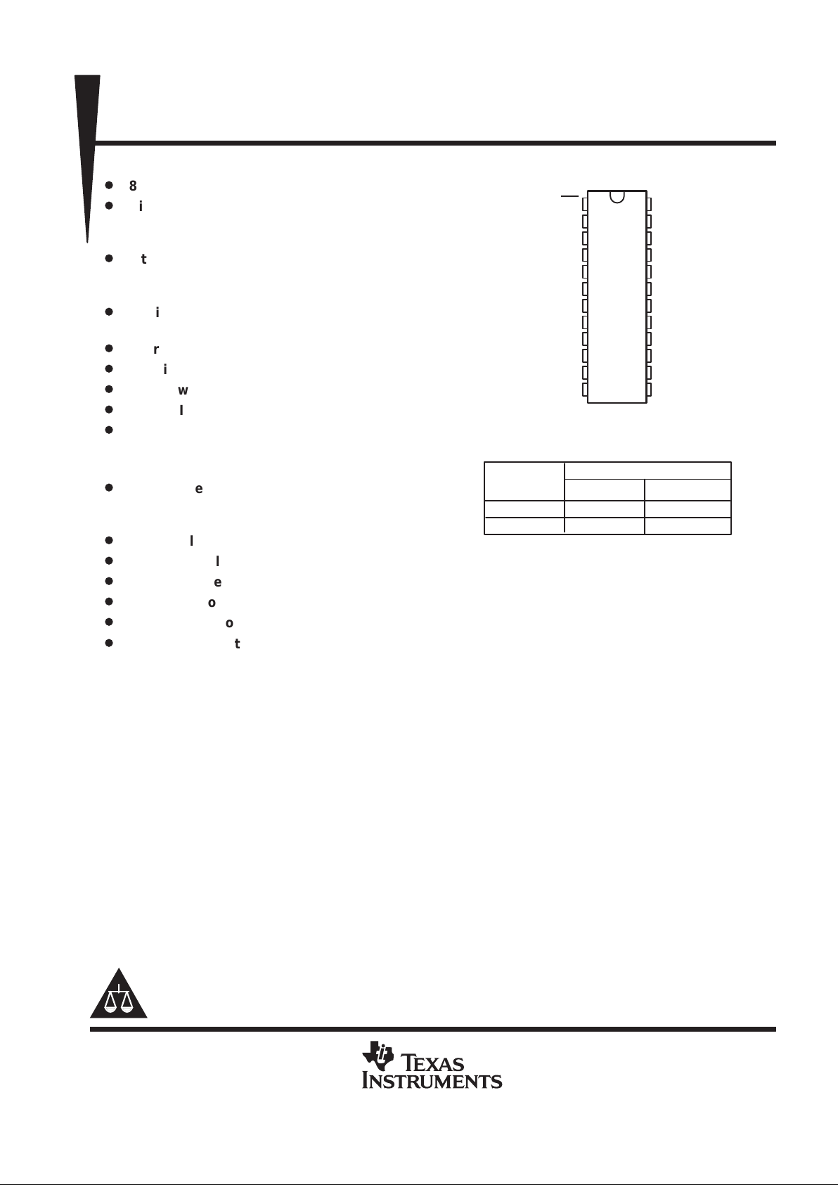
1
2
3
4
5
6
7
8
9
10
11
12
24
23
22
21
20
19
18
17
16
15
14
13
OE
DGND
D1(LSB)
D2
D3
D4
D5
D6
D7
D8(MSB)
V
DDD
CLK
DGND
REFB
REFBS
AGND
AGND
ANALOG IN
V
DDA
REFT
REFTS
V
DDA
V
DDA
V
DDD
PW OR NS PACKAGE
(TOP VIEW)
AVAILABLE OPTIONS
–0°C to 70°C
SOP (NS)
T
A
TLC5540CNSLE
PACKAGE
TSSOP (PW)
TLC5540CPW
–40°C to 85°C
TLC5540INSLE
TLC5540IPW
PRODUCTION DATA information is current as of publication date.
Products conform to specifications per the terms of Texas Instruments
standard warranty. Production processing does not necessarily include
testing of all parameters.
Copyright 1999, Texas Instruments Incorporated
Page 2
TLC5540
8-BIT HIGH-SPEED ANALOG-TO-DIGITAL CONVERTER
SLAS105C – JANUARY 1995 – REVISED MAY 1999
2
POST OFFICE BOX 655303 • DALLAS, TEXAS 75265
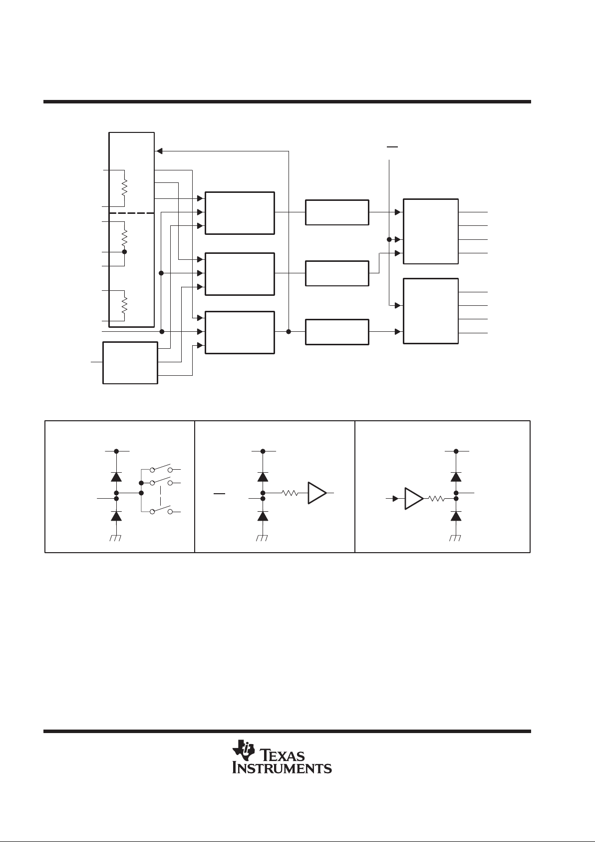
functional block diagram
Lower Sampling
Comparators
(4 Bit)
Lower Encoder
(4 Bit)
Lower Data
Latch
Lower Sampling
Comparators
(4 Bit)
Lower Encoder
(4 Bit)
Upper Sampling
Comparators
(4 Bit)
Upper Encoder
(4 Bit)
Upper Data
Latch
Clock
Generator
OE
D1(LSB)
D2
D3
D4
D5
D6
D7
D8(MSB)
CLK
REFB
REFT
REFBS
AGND
AGND
ANALOG IN
V
DDA
REFTS
270 Ω
NOM
80 Ω
NOM
320 Ω
NOM
Resistor
Reference
Divider
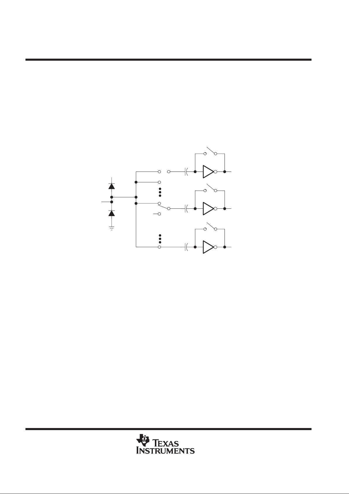
schematics of inputs and outputs
EQUIVALENT OF ANALOG INPUT
V
DDA
AGND
ANALOG IN
EQUIVALENT OF EACH DIGITAL INPUT
V
DDD
DGND
OE, CLK
EQUIVALENT OF EACH DIGITAL OUTPUT
V
DDD
DGND
D1–D8
Page 3
TLC5540
8-BIT HIGH-SPEED ANALOG-TO-DIGITAL CONVERTER
SLAS105C – JANUARY 1995 – REVISED MAY 1999
3
POST OFFICE BOX 655303 • DALLAS, TEXAS 75265
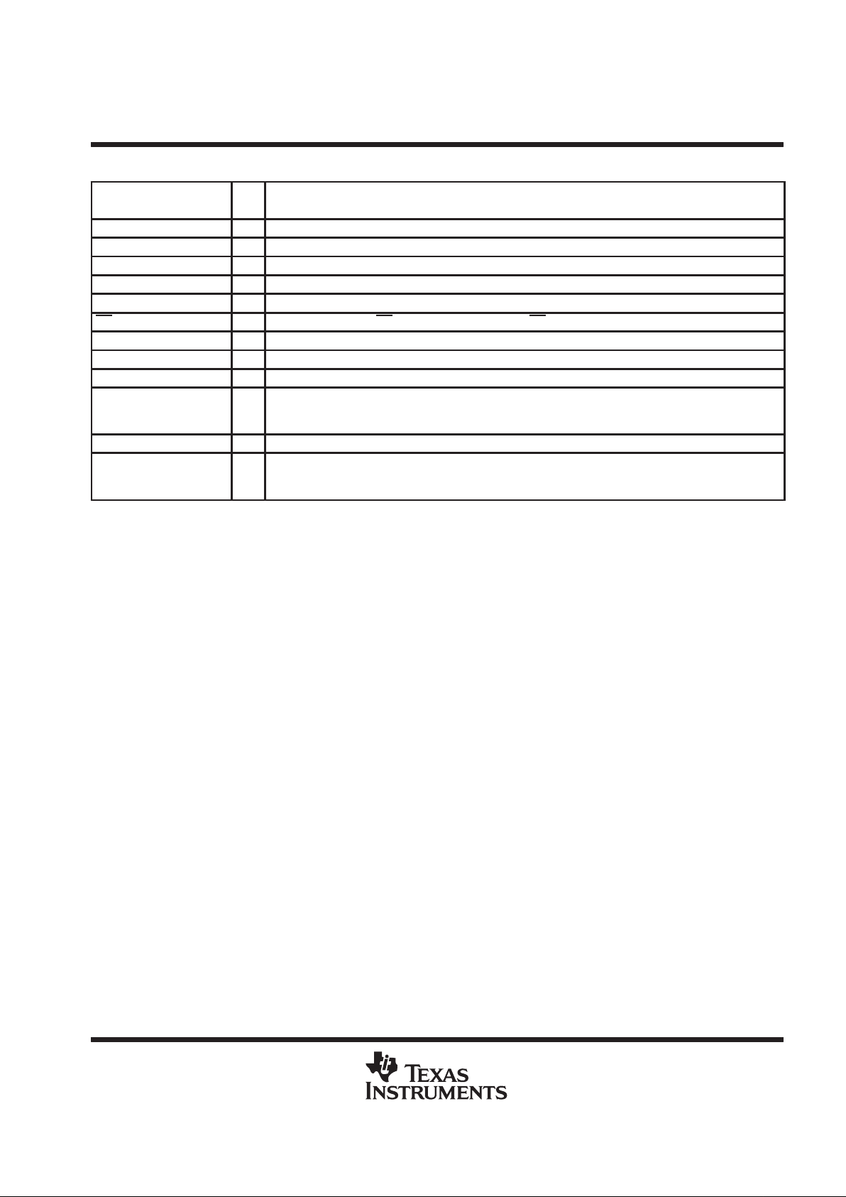
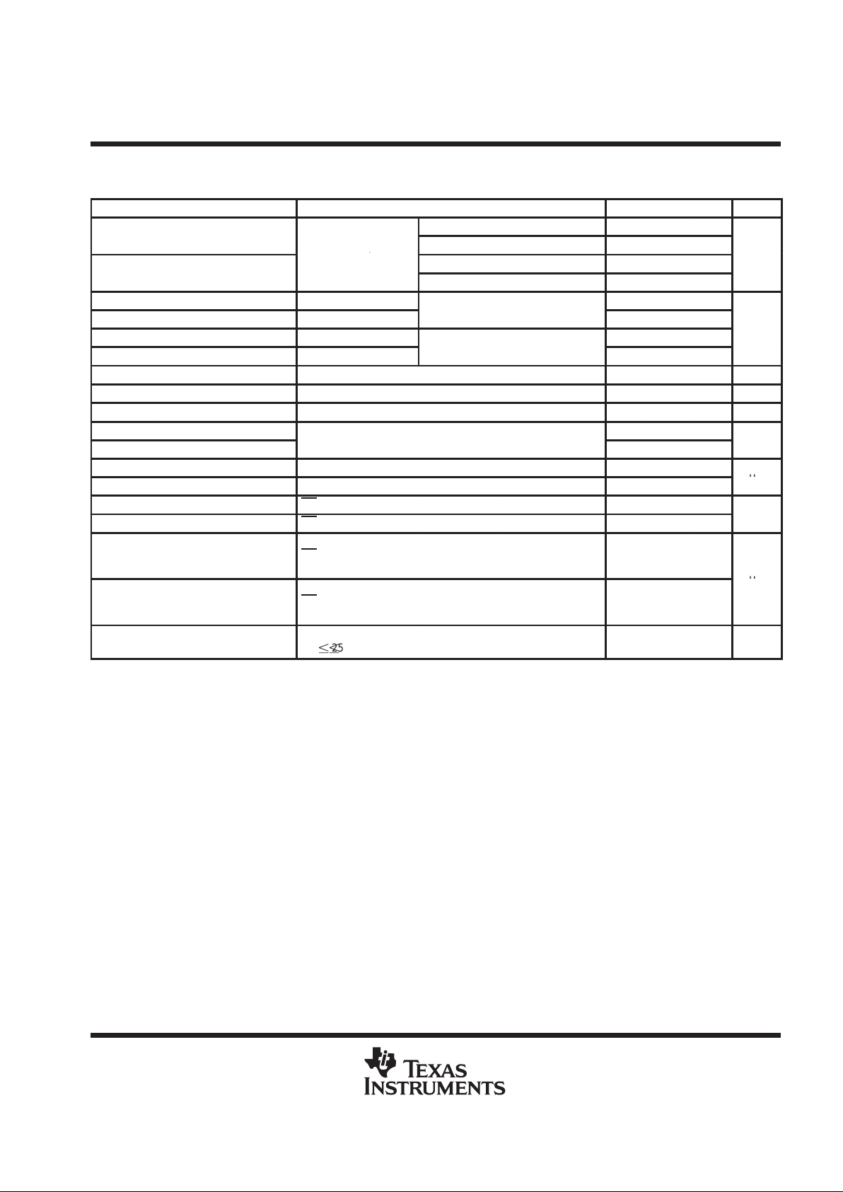
Terminal Functions
TERMINAL
NAME NO.
I/O
DESCRIPTION
AGND 20, 21 Analog ground
ANALOG IN 19 I Analog input
CLK 12 I Clock input
DGND 2, 24 Digital ground
D1–D8 3–10 O Digital data out. D1:LSB, D8:MSB
OE 1 I Output enable. When OE = L, data is enabled. When OE = H, D1–D8 is high impedance.
V
DDA
14, 15, 18 Analog V
DD
V
DDD
11, 13 Digital V
DD
REFB 23 I ADC reference voltage in (bottom)
REFBS 22 Reference voltage (bottom). When using the internal voltage divider to generate a nominal 2-V reference,
the REFBS terminal is shorted to the REFB terminal and the REFTS terminal is shorted to the REFT terminal
(see Figure 13 and Figure 14).
REFT 17 I Reference voltage in (top)
REFTS 16 Reference voltage (top). When using the internal voltage divider to generate a nominal 2-V reference, the
REFTS terminal is shorted to the REFT terminal and the REFBS terminal is shorted to the REFB terminal
(see Figure 13 and Figure 14).
absolute maximum ratings over operating free-air temperature range (unless otherwise noted)
†
Supply voltage, V
DDA
, V
DDD
7 V. . . . . . . . . . . . . . . . . . . . . . . . . . . . . . . . . . . . . . . . . . . . . . . . . . . . . . . . . . . . . . . . .
Reference voltage input range, V
I(REFT)
, V
I(REFB)
, V
I(REFBS)
, V
I(REFTS)
AGND to V
DDA
. . . . . . . . . . . . . . .
Analog input voltage range, V
I(ANLG)
AGND to V
DDA
. . . . . . . . . . . . . . . . . . . . . . . . . . . . . . . . . . . . . . . . . . . . . . .
Digital input voltage range, V
I(DGTL)
DGND to V
DDD
. . . . . . . . . . . . . . . . . . . . . . . . . . . . . . . . . . . . . . . . . . . . . . . .
Digital output voltage range, V
O(DGTL)
DGND to V
DDD
. . . . . . . . . . . . . . . . . . . . . . . . . . . . . . . . . . . . . . . . . . . . .
Operating free-air temperature range, T
A
: TLC5540C 0°C to 70°C. . . . . . . . . . . . . . . . . . . . . . . . . . . . . . . . . . .
TLC5540I –40°C to 85°C. . . . . . . . . . . . . . . . . . . . . . . . . . . . . . . . .
Storage temperature range, T
stg
–55°C to 150°C. . . . . . . . . . . . . . . . . . . . . . . . . . . . . . . . . . . . . . . . . . . . . . . . . . .
†
Stresses beyond those listed under “absolute maximum ratings” may cause permanent damage to the device. These are stress ratings only, and
functional operation of the device at these or any other conditions beyond those indicated under “recommended operating conditions” is not
implied. Exposure to absolute-maximum-rated conditions for extended periods may affect device reliability.
Page 4
TLC5540
8-BIT HIGH-SPEED ANALOG-TO-DIGITAL CONVERTER
SLAS105C – JANUARY 1995 – REVISED MAY 1999
4
POST OFFICE BOX 655303 • DALLAS, TEXAS 75265
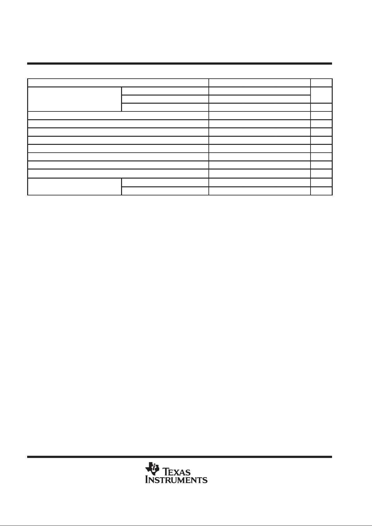
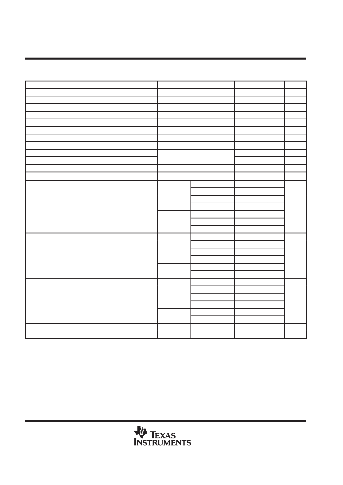
recommended operating conditions
MIN NOM MAX UNIT
V
DDA
–AGND 4.75 5 5.25
Supply voltage
V
DDD
–AGND 4.75 5 5.25
V
AGND–DGND –100 0 100 mV
Reference input voltage (top), V
I(REFT)
V
I(REFB)
+1.8 V
I(REFB)
+2 V
DDA
V
Reference input voltage (bottom), V
I(REFB)
0 0.6 V
I(REFT)
–1.8 V
Analog input voltage range, V
I(ANLG)
(see Note 1) V
I(REFB)
V
I(REFT)
V
Full scale voltage, V
I(REFT)
– V
I(REFB)
1.8 5 V
High-level input voltage, V
IH
4 V
Low-level input voltage, V
IL
1 V
Pulse duration, clock high, t
w(H)
12.5 ns
Pulse duration, clock low, t
w(L)
12.5 ns
p
p
TLC5540C 0 70 °C
Operating free-air temperature, T
A
TLC5540I –40 85 °C
NOTE 1: 1.8 V ≤ V
I(REFT)
– V
I(REFB)
< V
DD
Page 5
TLC5540
8-BIT HIGH-SPEED ANALOG-TO-DIGITAL CONVERTER
SLAS105C – JANUARY 1995 – REVISED MAY 1999
5
POST OFFICE BOX 655303 • DALLAS, TEXAS 75265
electrical characteristics at VDD = 5 V, V
I(REFT)
= 2.6 V, V
I(REFB)
= 0.6 V, fs = 40 MSPS, TA = 25°C
(unless otherwise noted)
PARAMETER TEST CONDITIONS
†
MIN TYP MAX UNIT
TA = 25°C ±0.6 ±1
ELLinearity error, integral
f
= 40 MSPS,
TA = MIN to MAX ±1
s
,
VI = 0.6 V to 2.6 V
TA = 25°C ±0.3 ±0.75
LSB
EDLinearity error, differential
TA = MIN to MAX ±1
Self bias (1), V
RB
Short REFB to REFBS
0.57 0.61 0.65
Self bias (1), V
RT
Short REFT to REFTS
See Figure 13
2.47 2.63 2.80
Self bias (2), V
RB
Short REFB to AGND
AGND
V
Self bias (2), V
RT
Short REFT to REFTS
See Figure 14
2.18 2.29 2.4
I
ref
Reference-voltage current V
I(REFT)
– V
I(REFB)
= 2 V 5.2 7.5 12 mA
R
ref
Reference-voltage resistor Between REFT and REFB terminals 165 270 350 Ω
C
i
Analog input capacitance V
I(ANLG)
= 1.5 V + 0.07 V
rms
4 pF
E
ZS
Zero-scale error
–18 –43 –68
E
FS
Full-scale error
V
I(REFT)
–
V
I(REFB)
= 2
V
–25 0 25
mV
I
IH
High-level input current VDD = 5.25 V , VIH = V
DD
5
I
IL
Low-level input current VDD = 5.25 V , VIL = 0 5
µ
A
I
OH
High-level output current OE = GND, VDD = 4.75 V , VOH = VDD–0.5 V –1.5
I
OL
Low-level output current OE = GND, VDD = 4.75 V , VOL = 0.4 V 2.5
mA
I
OZH(lkg)
High-level
high-impedance-state
output leakage current
OE = VDD, VDD = 5.25, VOH = V
DD
16
I
OZL(lkg)
Low-level
high-impedance-state
output leakage current
OE = VDD, VDD = 4.75, VOL = 0 16
µ
A
I
DD
Supply current
fs = 40 MSPS,
CL 25 pF,
NTSC‡ ramp wave input,
See Note 2
17 27 mA
†
Conditions marked MIN or MAX are as stated in recommended operating conditions.
‡
National Television System Committee
NOTE 2: Supply current specification does not include I
ref
.
Page 6
TLC5540
8-BIT HIGH-SPEED ANALOG-TO-DIGITAL CONVERTER
SLAS105C – JANUARY 1995 – REVISED MAY 1999
6
POST OFFICE BOX 655303 • DALLAS, TEXAS 75265
operating characteristics at VDD = 5 V, VRT = 2.6 V, VRB = 0.6 V, fs = 40 MSPS, TA = 25°C (unless
otherwise noted)
PARAMETER TEST CONDITIONS
†
MIN TYP MAX UNIT
f
s
Maximum conversion rate TA = MIN to MAX 40 MSPS
f
s
Minimum conversion rate TA = MIN to MAX 5 MSPS
BW Analog input full-power bandwidth At – 3 dB, V
I(ANLG)
= 2 V
pp
75 MHz
t
pd
Delay time, digital output CL ≤ 10 pF (see Note 3) 9 15 ns
t
PHZ
Disable time, output high to Hi-Z CL ≤ 15 pF, IOH = –4.5 mA 20 ns
t
PLZ
Disable time, output low to Hi-Z CL ≤ 15 pF, IOL = 5 mA 20 ns
t
PZH
Enable time, Hi-Z to output high CL ≤ 15 pF, IOH = –4.5 mA 15 ns
t
PZL
Enable time, Hi-Z to output low CL ≤ 15 pF, IOL = 5 mA 15 ns
Differential gain
NTSC 40 IRE‡ modulation wave
,
1%
Differential phase
NTSC 40 IRE modulation wave,
fs = 14.3 MSPS
0.7 degrees
t
AJ
Aperture jitter time 30 ps
t
d(s)
Sampling delay time 4 ns
fI = 1 MHz 47
fI = 3 MHz 44 47
f
s
=
20 MSPS
fI = 6 MHz 46
SNR Signal-to-noise ratio
fI = 10 MHz 45
dB
fI = 3 MHz 45.2
fs = 40 MSPS
fI = 6 MHz 42 44
fI = 10 MHz 42
fI = 1 MHz 7.64
fI = 3 MHz 7.61
f
s
= 20
MSPS
fI = 6 MHz 7.47
ENOB
Effective number of bits
fI = 10 MHz 7.16
Bits
fI = 3 MHz 7
f
s
= 40
MSPS
fI = 6 MHz 6.8
fI = 1 MHz 43
fI = 3 MHz 35 42
f
s
= 20
MSPS
fI = 6 MHz 41
THD
Total harmonic distortion
fI = 10 MHz 38
dBc
fI = 3 MHz 40
f
s
= 40
MSPS
fI = 6 MHz 38
p
fs = 20 MSPS
41 46
Spurious free dynamic range
fs = 40 MSPS
f
I
=
3 MH
z
42
dBc
†
Conditions marked MIN or MAX are as stated in recommended operating conditions.
‡
Institute of Radio Engineers
NOTE 3: CL includes probe and jig capacitance.
Page 7

TLC5540
8-BIT HIGH-SPEED ANALOG-TO-DIGITAL CONVERTER
SLAS105C – JANUARY 1995 – REVISED MAY 1999
7
POST OFFICE BOX 655303 • DALLAS, TEXAS 75265
PARAMETER MEASUREMENT INFORMATION
N
N+1
N+2
N+3
N+4
N–3 N–2 N–1 N N+1
t
pd
CLK (Clock)
ANALOG IN
(Input Signal)
D1–D8
(Output Data)
t
w(H)
t
w(L)
Figure 1. I/O Timing Diagram
t
PZH
OE
Data Output
t
PHZ
Active
Active
Hi-Z
Reference Level
(2.5 V)
2.4 V
0.4 V
t
PZL
t
PLZ
Figure 2. I/O Timing Diagram
Page 8
TLC5540
8-BIT HIGH-SPEED ANALOG-TO-DIGITAL CONVERTER
SLAS105C – JANUARY 1995 – REVISED MAY 1999
8
POST OFFICE BOX 655303 • DALLAS, TEXAS 75265
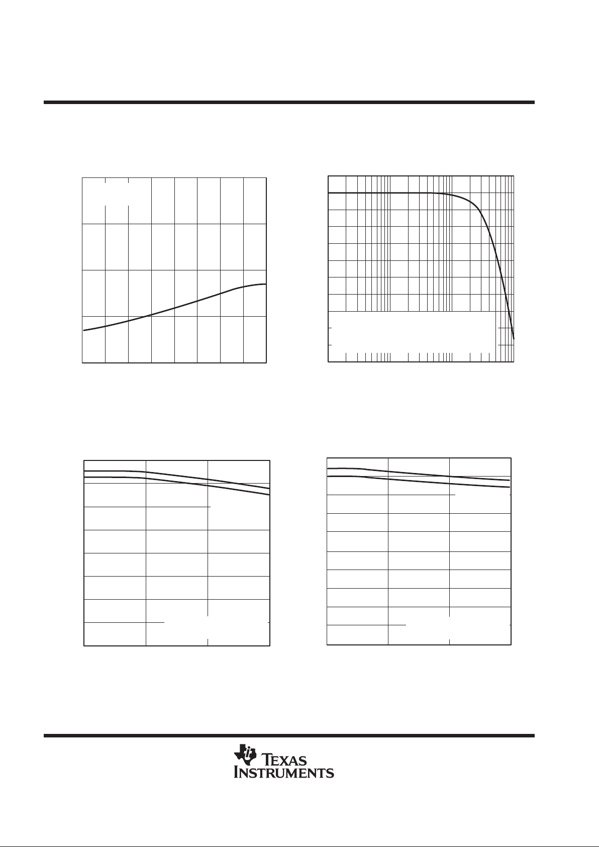
TYPICAL CHARACTERISTICS
Figure 3
Power Dissipation – mW
POWER DISSIPATION
vs
SAMPLING FREQUENCY
100
50
0
0 5 10 20
150
200
30
fs – Sampling Frequency – MHz
VDD = 5 V
TA = 25°C
15
25 35 40
Figure 4
0.1 1 10 100
Gain – dB
ANALOG INPUT BANDWIDTH
0.5
0
–0.5
–1
–1.5
–2
–2.5
–3
–4
–4.5
–5
VCC = 5 V, VRT = 2.6 V, VRB = 0.6 V
CLK = 40 MHz
ANALOG IN = 100 k – 100 MHz Sine Wave
VI = 2 V
(PP)
fI – Input Frequency – MHz
–3.5
Figure 5
ENOB – Effective Number of Bits – BITS
EFFECTIVE NUMBER OF BITS
vs
INPUT FREQUENCY
fI – Input Frequency – MHz
2
0
8
4
0 5 10 15
6
1
3
5
7
fs = 20 MHz
VDD = 5 V, VI = 1 V
(PP)
VRB = 2.6 V, VRT = 0.6 V
fs = 40 MHz
Figure 6
SNR – Signal-to-Noise Ratio – dB
SIGNAL-TO-NOISE RATIO
vs
INPUT FREQUENCY
fI – Input Frequency – MHz
30
20
10
0
0510
40
50
15
VDD = 5 V, VI = 1 V
(PP)
VRB = 2.6 V, VRT = 0.6 V
fs = 20 MHz
5
15
25
35
45
fs = 40 MHz
Page 9

TLC5540
8-BIT HIGH-SPEED ANALOG-TO-DIGITAL CONVERTER
SLAS105C – JANUARY 1995 – REVISED MAY 1999
9
POST OFFICE BOX 655303 • DALLAS, TEXAS 75265
TYPICAL CHARACTERISTICS
Figure 7
–1
–0.2
–0.4
–0.6
–0.8
0 40 80 120 160
200 240
0
0.8
0.6
0.4
0.2
1
DIFFERENTIAL NONLINEARITY
VI = V
ramp
= 0.6 V – 2.6 V, 500 Hz
VRT = 2.6 V , VRB = 0.6 V , VDD = 5 V
fs = 40 MHz
TA = 25°C
Differential Nonlinearity – LSB
Digital Output Code
Figure 8
7
6.5
6
ENOB – Effective Number of Bits – BITS
7.5
EFFECTIVE NUMBER OF BITS
vs
AMBIENT TEMPERATURE
8
–40 0 20 40 60
TA – Ambient Temperature – °C
–20 80 100
VDD = 5 V, VI = 1 V
(PP)
, 3 MHz Sine Wave
VRT = 2.6 V , VRB = 0.6 V, fs = 20 MHz
Figure 9
–1
–0.2
–0.4
–0.6
–0.8
0 40 80 120 160
200 240
0
0.8
0.6
0.4
0.2
1
Integral Nonlinearity – LSB
Digital Output Code
INTEGRAL NONLINEARITY
VI = V
ramp
= 0.6 V – 2.6 V, 500 Hz
VRT = 2.6 V , VRB = 0.6 V , VDD = 5 V
fs = 40 MHz, TA = 25°C
Figure 10
Magnitude – dB
–100
f – Frequency – MHz
–60
–70
–80
–90
01 23 4 567 8
910
FFT SPECTRUM
VI = 2 V
(PP)
, 1 MHz Sine Wave
VRT = 2.6 V , VRB = 0.6 V
fs = 20 MHz, TA = 25°C
–50
–10
–20
–30
–40
0
Page 10
TLC5540
8-BIT HIGH-SPEED ANALOG-TO-DIGITAL CONVERTER
SLAS105C – JANUARY 1995 – REVISED MAY 1999
10
POST OFFICE BOX 655303 • DALLAS, TEXAS 75265
APPLICATION INFORMATION
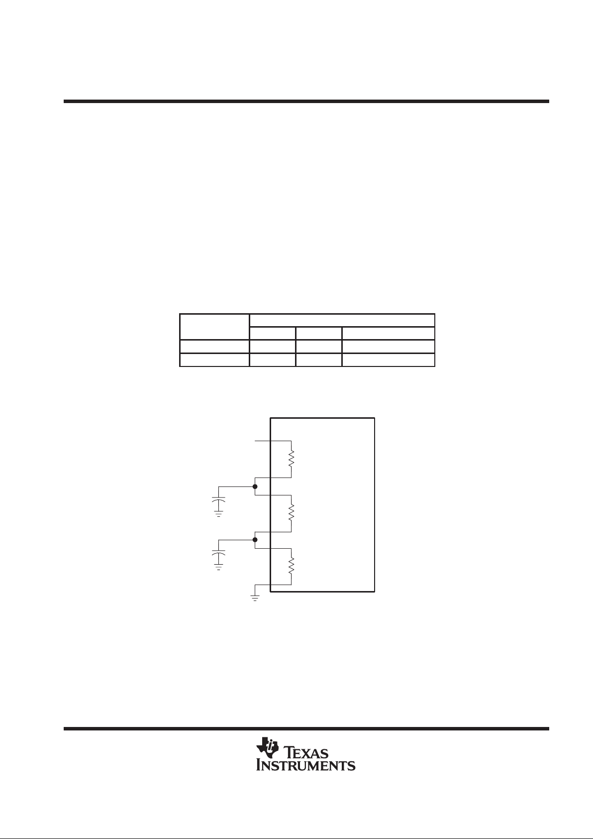
grounding and power supply considerations
A signal ground is a low-impedance path for current to return to the source. Inside the TLC5540 A/D converter,
the analog ground and digital ground are connected to each other through the substrate, which has a very small
resistance (~30 Ω) to prevent internal latch-up. For this reason, it is strongly recommended that a printed circuit
board (PCB) of at least 4 layers be used with the TLC5540 and the converter DGND and AGND pins be
connected directly to the analog ground plane to avoid a ground loop. Figure 11 shows the recommended
decoupling and grounding scheme for laying out a multilayer PC board with the TLC5540. This scheme ensures
that the impedance connection between AGND and DGND is minimized so that their potential difference is
negligible and noise source caused by digital switching current is eliminated.
0.1 µF 0.1 µF
11 13 24 2 14 15 18 20 21
V
DDD
GND V
DDA
AGND
TLC5540
Signal Plane
Analog Ground Plane
Analog Supply Plane
Signal Plane
Digital Supply Plane
0.1 µF 0.1 µF 0.1 µF
Figure 11. AVDD, DVDD, AGND, and DGND Connections
printed circuit board (PCB) layout considerations
When designing a circuit that includes high-speed digital and precision analog signals such as a high speed
ADC, PCB layout is a key component to achieving the desired performance. The following recommendations
should be considered during the prototyping and PCB design phase:
D
Separate analog and digital circuitry physically to help eliminate capacitive coupling and crosstalk. When
separate analog and digital ground planes are used, the digital ground and power planes should be several
layers from the analog signals and power plane to avoid capacitive coupling.
D
Full ground planes should be used. Do not use individual etches to return analog and digital currents or
partial ground planes. For prototyping, breadboards should be constructed with copper clad boards to
maximize ground plane.
D
The conversion clock, CLK, should be terminated properly to reduce overshoot and ringing. Any jitter on
the conversion clock degrades ADC performance. A high-speed CMOS buffer such as a 74ACT04 or
74AC04 positioned close to the CLK terminal can improve performance.
D
Minimize all etch runs as much as possible by placing components very close together. It also proves
beneficial to place the ADC in a corner of the PCB nearest to the I/O connector analog terminals.
D
It is recommended to place the digital output data latch (if used) as close to the TLC5540 as possible to
minimize capacitive loading. If D0 through D7 must drive large capacitive loads, internal ADC noise may
be experienced.
Page 11

TLC5540
8-BIT HIGH-SPEED ANALOG-TO-DIGITAL CONVERTER
SLAS105C – JANUARY 1995 – REVISED MAY 1999
11
POST OFFICE BOX 655303 • DALLAS, TEXAS 75265
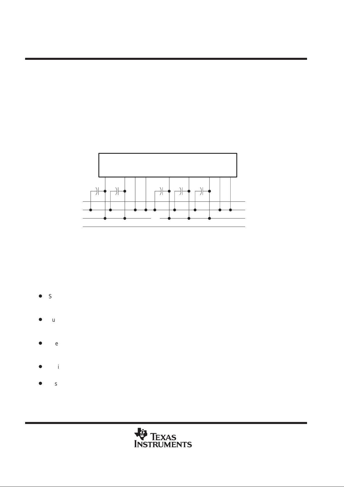
PRINCIPLES OF OPERATION
functional description
The TLC5540 uses a modified semiflash architecture as shown in the functional block diagram. The four most
significant bits (MSBs) of every output conversion result are produced by the upper comparator block CB1. The
four least significant bits (LSBs) of each alternate output conversion result are produced by the lower
comparator blocks CB-A and CB-B in turn (see Figure 12).
The reference voltage that is applied to the lower comparator resistor string is one sixteenth of the amplitude
of the refence applied to the upper comparator resistor string. The sampling comparators of the lower
comparator block require more time to sample the lower voltages of the reference and residual input voltage.
By applying the residual input voltage to alternate lower comparator blocks, each comparator block has twice
as much time to sample and convert as would be the case if only one lower comparator block were used.
VI(1) VI(2) VI(3) VI(4)
CLK1 CLK2 CLK3 CLK4
S(1) C(1) S(2) C(2) S(3) C(3) S(4) C(4)
S(1) H(1) C(1) S(3) H(3) C(3)
H(0) C(0) S(2) H(2) C(2) S(4) H(4)
LD(–2)
OUT(–2) OUT(–1) OUT(0) OUT(1)
ANALOG IN
(Sampling Points)
CLK (Clock)
Upper Comparators Block (CB1)
Upper Data
Lower Reference Voltage
Lower Comparators Block (CB-A)
Lower Data (A)
Lower Comparators Block (CB-B)
Lower Data (B)
D1–D8 (Data Output)
UD(0)
RV(0)
UD(1)
RV(1)
UD(2)
RV(2)
UD(3)
RV(3)
LD(–1)
LD(0)
LD(1)
LD(2)
t
pd
Figure 12. Internal Functional Timing Diagram
This conversion scheme, which reduces the required sampling comparators by 30 percent compared to
standard semiflash architectures, achieves significantly higher sample rates than the conventional semiflash
conversion method.
Page 12
TLC5540
8-BIT HIGH-SPEED ANALOG-TO-DIGITAL CONVERTER
SLAS105C – JANUARY 1995 – REVISED MAY 1999
12
POST OFFICE BOX 655303 • DALLAS, TEXAS 75265
PRINCIPLES OF OPERATION
functional description (continued)
The MSB comparator block converts on the falling edge of each applied clock cycle. The LSB comparator blocks
CB-A and CB-B convert on the falling edges of the first and second following clock cycles, respectively. The
timing diagram of the conversion algorithm is shown in Figure 12.
analog input operation
The analog input stage to the TLC5540 is a chopper-stabilized comparator and is equivalently shown below:
V
DDA
ANALOG IN
S1
V
ref(N)
φ1
φ2
φ2
S3
φ1
C
s
To Encoder Logic
φ2
S2
φ1
C
s
To Encoder Logic
φ2
S(N)
φ1
C
s
To Encoder Logic
Figure 13. External Connections for Using the Internal Reference Resistor Divider
Figure 13 depicts the analog input for the TLC5540. The switches shown are controlled by two internal clocks,
φ1 and φ2. These are nonoverlapping clocks that are generated from the CLK input. During the sampling period,
φ1, S1 is closed and the input signal is applied to one side of the sampling capacitor, C
s
. Also during the sampling
period, S2 through S(N) are closed. This sets the comparator input to approximately 2.5 V. The delta voltage
is developed across C
s
. During the comparison phase, φ2, S1 is switched to the appropriate reference voltage
for the bit value N. S2 is opened and V
ref(N)
– VC
s
toggles the comparator output to the appropriate digital 1 or
0. The small resistance values for the switch, S1, and small value of the sampling capacitor combine to produce
the wide analog input bandwidth of the TLC5540. The source impedance driving the analog input of the
TLC5540 should be less than 100 Ω across the range of input frequency spectrum.
reference inputs – REFB, REFT, REFBS, REFTS
The range of analog inputs that can be converted are determined by REFB and REFT, REFT being the
maximum reference voltage and REFB being the minimum reference voltage. The TLC5540 is tested with
REFT = 2.6 V and REFB = 0.6 V producing a 2-V full-scale range. The TLC5540 can operate with
REFT – REFB = 5 V, but the power dissipation in the reference resistor increases significantly (93 mW
nominally). It is recommended that a 0.1 µF capacitor be attached to REFB and REFT whether using externally
or internally generated voltages.
Page 13
TLC5540
8-BIT HIGH-SPEED ANALOG-TO-DIGITAL CONVERTER
SLAS105C – JANUARY 1995 – REVISED MAY 1999
13
POST OFFICE BOX 655303 • DALLAS, TEXAS 75265
PRINCIPLES OF OPERATION
internal reference voltage conversion
Three internal resistors allow the device to generate an internal reference voltage. These resistors are brought
out on terminals V
DDA
, REFTS, REFT, REFB, REFBS, and AGND. Two different bias voltages are possible
without the use of external resistors.
Internal resistors are provided to develop REFT = 2.6 V and REFB = 0.6 V (bias option one) with only two
external connections. This is developed with a 3-resistor network connected to V
DDA
. When using this feature,
connect REFT to REFTS and connect REFB to REFBS. For applications where the variance associated with
V
DDA
is acceptable, this internal voltage reference saves space and cost (see Figure 14).
A second internal bias option (bias two option) is shown in Figure 15. Using this scheme REFB = AGND and
REFT = 2.28 V nominal. These bias voltage options can be used to provide the values listed in the following
table.
Table 1. Bias Voltage Options
BIAS VOLTAGE
BIAS OPTION
V
RB
V
RT
VRT – V
RB
1 0.61 2.63 2.02
2 AGND 2.28 2.28
To use the internally-generated reference voltage, terminal connections should be made as shown in
Figure 14 or Figure 15. The connections in Figure 14 provide the standard video 2-V reference.
R1
320 Ω NOM
R
ref
270 Ω NOM
R2
80 Ω NOM
V
DDA
5 V (Analog)
REFTS
REFT
REFB
REFBS
AGND
TLC5540
16
17
22
21
23
18
0.1 µF
0.1 µF
2.63 V dc
0.61 V dc
Figure 14. External Connections Using the Internal Bias One Option
Page 14

TLC5540
8-BIT HIGH-SPEED ANALOG-TO-DIGITAL CONVERTER
SLAS105C – JANUARY 1995 – REVISED MAY 1999
14
POST OFFICE BOX 655303 • DALLAS, TEXAS 75265
PRINCIPLES OF OPERATION
R1
320 Ω NOM
R
ref
270 Ω NOM
R2
80 Ω NOM
V
DDA
5 V (Analog)
REFTS
REFT
REFB
REFBS
AGND
TLC5540
16
17
22
21
23
18
0.1 µF
2.28 V dc
0 V dc
Figure 15. External Connections Using the Internal Bias Two Option
functional operation
Table 2 shows the TLC5540 functions.
Table 2. Functional Operation
INPUT SIGNAL
DIGITAL OUTPUT CODE
INPUT SIGNAL
VOLTAGE
STEP
MSB LSB
V
ref(T)
255 1 1 1 1 1 1 1 1
•
• • •••••••
• • ••••••••
• 128 1 0000000
• 127 0 1111111
• • • •••••••
• • ••••••••
V
ref(B)
0 0 0 0 0 0 0 0 0
Page 15

TLC5540
8-BIT HIGH-SPEED ANALOG-TO-DIGITAL CONVERTER
SLAS105C – JANUARY 1995 – REVISED MAY 1999
15
POST OFFICE BOX 655303 • DALLAS, TEXAS 75265
MECHANICAL DATA
PW (R-PDSO-G**) PLASTIC SMALL-OUTLINE PACKAGE
14 PINS SHOWN
0,65
M
0,10
0,10
0,25
0,50
0,75
0,15 NOM
Gage Plane
28
9,80
9,60
24
7,90
7,70
2016
6,60
6,40
4040064/F 01/97
0,30
6,60
6,20
8
0,19
4,30
4,50
7
0,15
14
A
1
1,20 MAX
14
5,10
4,90
8
3,10
2,90
A MAX
A MIN
DIM
PINS **
0,05
4,90
5,10
Seating Plane
0°–8°
NOTES: A. All linear dimensions are in millimeters.
B. This drawing is subject to change without notice.
C. Body dimensions do not include mold flash or protrusion not to exceed 0,15.
D. Falls within JEDEC MO-153
Page 16

TLC5540
8-BIT HIGH-SPEED ANALOG-TO-DIGITAL CONVERTER
SLAS105C – JANUARY 1995 – REVISED MAY 1999
16
POST OFFICE BOX 655303 • DALLAS, TEXAS 75265
MECHANICAL DATA
NS (R-PDSO-G**) PLASTIC SMALL-OUTLINE PACKAGE
4040062/B 10/94
14 PIN SHOWN
2,00 MAX
A
0,05 MIN
Seating Plane
1,05
0,55
1
14
PINS **
5,60
5,00
7
8,20
7,40
8
A MIN
A MAX
DIM
Gage Plane
0,15 NOM
0,25
9,90 9,90
10,501410,50
16
12,30 14,70
15,3012,90
20 24
0,10
1,27
0°–10°
M
0,25
0,35
0,51
NOTES: A. All linear dimensions are in millimeters.
B. This drawing is subject to change without notice.
C. Body dimensions do not include mold flash or protrusion, not to exceed 0,15.
Page 17

IMPORTANT NOTICE
T exas Instruments and its subsidiaries (TI) reserve the right to make changes to their products or to discontinue
any product or service without notice, and advise customers to obtain the latest version of relevant information
to verify, before placing orders, that information being relied on is current and complete. All products are sold
subject to the terms and conditions of sale supplied at the time of order acknowledgement, including those
pertaining to warranty, patent infringement, and limitation of liability.
TI warrants performance of its semiconductor products to the specifications applicable at the time of sale in
accordance with TI’s standard warranty. Testing and other quality control techniques are utilized to the extent
TI deems necessary to support this warranty. Specific testing of all parameters of each device is not necessarily
performed, except those mandated by government requirements.
CERT AIN APPLICATIONS USING SEMICONDUCTOR PRODUCTS MAY INVOLVE POTENTIAL RISKS OF
DEATH, PERSONAL INJURY, OR SEVERE PROPERTY OR ENVIRONMENTAL DAMAGE (“CRITICAL
APPLICATIONS”). TI SEMICONDUCTOR PRODUCTS ARE NOT DESIGNED, AUTHORIZED, OR
WARRANTED TO BE SUITABLE FOR USE IN LIFE-SUPPORT DEVICES OR SYSTEMS OR OTHER
CRITICAL APPLICATIONS. INCLUSION OF TI PRODUCTS IN SUCH APPLICA TIONS IS UNDERST OOD TO
BE FULLY AT THE CUSTOMER’S RISK.
In order to minimize risks associated with the customer’s applications, adequate design and operating
safeguards must be provided by the customer to minimize inherent or procedural hazards.
TI assumes no liability for applications assistance or customer product design. TI does not warrant or represent
that any license, either express or implied, is granted under any patent right, copyright, mask work right, or other
intellectual property right of TI covering or relating to any combination, machine, or process in which such
semiconductor products or services might be or are used. TI’s publication of information regarding any third
party’s products or services does not constitute TI’s approval, warranty or endorsement thereof.
Copyright 1999, Texas Instruments Incorporated
 Loading...