

Page 1
TI
Sitara™ARM
Microprocessors
Microprocessors
Yair Hougui
Application Engineer
1
Page 2
TI Embedded Processors Portfolio
TI Embedded Processors
32-bit ARM
16-bit ultra-
High-
ARM
Low-power
TI Embedded Processors
Digital Signal Processors (DSPs)Microcontrollers (MCUs)
ARM®-Based Processors
32-bit
Cortex
™-M3
MCUs
low power
MCUs
performance
DSPs
Cortex
-
A8
MPUs
DSPs
Stellaris
®
®
C5000
™
MSP430
™
Sitara
™
ARM® Cortex™-A8
C6000
™
DaVinci
™
real-time
MCUs
C2000
™
Delfino
™
ARM
Cortex™
-
M3
& ARM9
OMAP
™
Up to
100 MHz
Flash
64 KB to 256 KB
300MHz to
>1GHz
Cache,
RAM, ROM
Up to
25 MHz
Flash
1 KB to 256 KB
Up to 300 MHz
+Accelerator
Up to 320KB RAM
Up to 128KB ROM
300MHz to >1GHz
+Accelerator
Cache
RAM, ROM
Piccolo
™
40MHz to
300 MHz
Flash, RAM
16 KB to 512 KB
USB, ENET MAC+PHY
CAN, ADC, PWM, SPI
Connectivity, Security,
Motion Control, HMI,
Industrial Automation
RAM, ROM
USB, CAN,
PCIe, EMAC
Industrial computing,
POS & portable
data terminals
1 KB to 256 KB
Analog I/O, ADC
LCD, USB, RF
Measurement,
Sensing, General
Purpose
Up to 128KB ROM
USB, ADC
McBSP, SPI, I2C
Port. Telecom, audio,
medical monitor
& diag, industrial
RAM, ROM
USB, ENET,
PCIe, SATA, SPI
Test & Meas., Video,
audio, security,
imaging, infrastructure
PWM, ADC,
CAN, SPI, I2C
Motor Control,
Digital Power,
Lighting, Ren. Energy
$1.00 to $8.00
$5.00 to $20.00
$0.49 to $9.00
$3.00 to $10.00
$5.00 to $200.00
$1.50 to $20.00
2
MPUs – Microprocessors
Software & Dev. Tools
Page 3
What is Sitara™?
• High-level operating system
• 300MHz – 1GHz+ in future devices
Ideal for applications requiring
• New platform of high-performance
ARM microprocessors:
What’s new
•
Advanced graphical user interfaces
• Flexible connectivity and multiple
interface options
• High system integration
–
ARM9 to ARM
®
Cortex
™
-
A8 MPU’s
• First new devices:
– AM35xx & AM17xx/AM18xx
•
Coming soon:
•
And…
• Scalability
• System cost constraints
• Application software portability
•
Coming soon:
– , AM3703/AM3715
• Software compatible roadmap
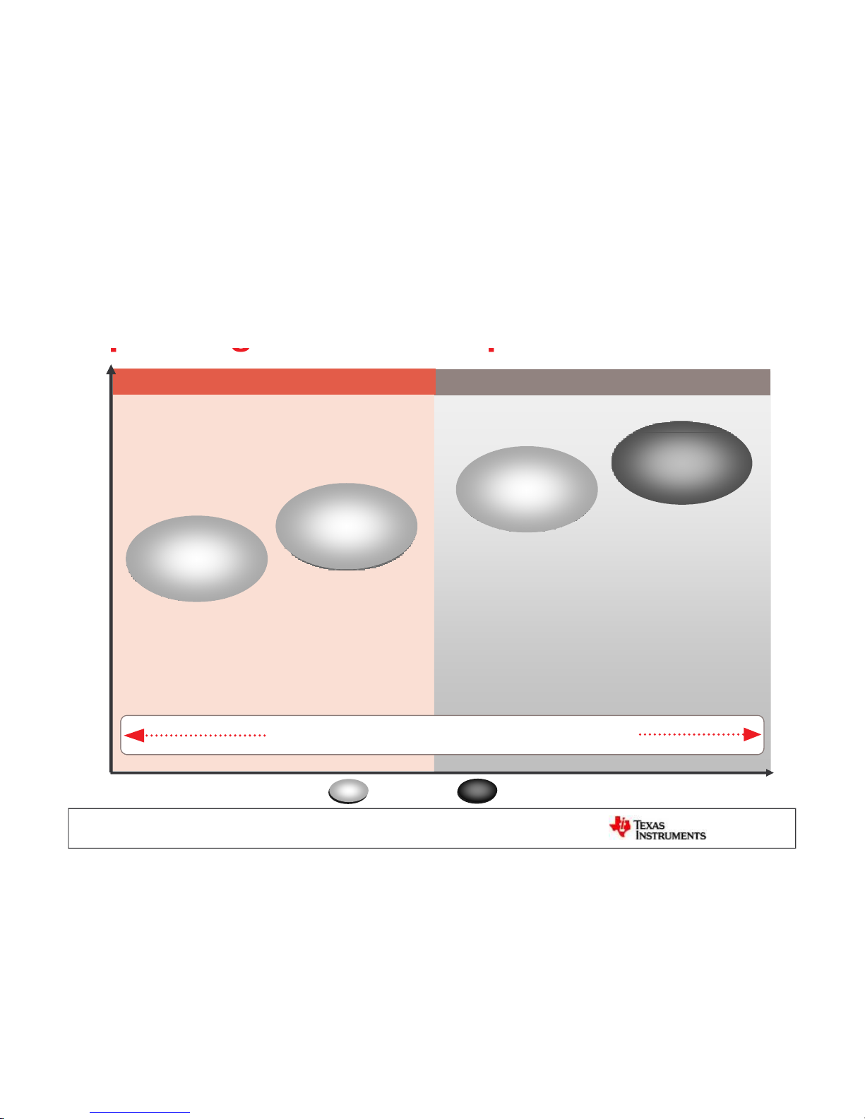
Sitara ARM MPUs – a good fit for industrial, instrumentation, POS
Industrial
automation
Point
Medical
instrumentation
HVAC and
building
of service
Test &
Single
3
building
controls
measurement
board
computing
Page 4
Sitara
™
ARM
®
microprocessors
In Development
ARM Cortex-A8ARM9
Available Now
ARM Cortex-A8
AM37xx (2Q10)
“AM38x Next” (2011)
“AM33x Next” (2011)
AM1705
AM1707
AM1806
OMAP3503
OMAP3515
AM3505
AM1808
AM3517
Higher Performance Cortex-
A8 with enhanced integration
• Up to 2000 DMIPS
Low power ARM9 with
Integrated peripherals
• Power efficient (down to 7mW
Advanced ARM Cortex-A8
with system integration
• Up to 1440 DMIPS
•
Power efficient (down to 10mW
standby, 1W active)
• Enhanced graphics/UI
• Enhanced integrated
peripherals, 1Gb Ethernet,
standby, 182mW active)
• Cost efficient
• Flexible industrial I/O PRU (CAN,
UART)
• Integrated peripherals, 10/100
•
Integrated interfaces to display,
USB, 10/100 Ethernet, SD card,
Wi-Fi®, CAN, and many others
• Integrated graphics for rich user
interface functions
4
PCIe
Ethernet, USB, SATA, and many
more
Page 5
Develop product designs with TI’s
expanding Sitara
™
MPU portfolio
expanding Sitara
MPU portfolio
Cortex™-A8
ARM926
AM37x
Sampling
AM35x
• High performance general purpose
AM18x
AM17x
Performance
• Power and cost-efficient
• Flexible industrial I/O
• Up to 450 MHz (495 DMIPS)
processor
• Advanced graphics/UI
• Roadmap to > 1 GHz (>2000 DMIPS)
•
Starting @ $5 (1ku)
Linux and Windows®Embedded CE kernel & drivers
Example code & demos
5
Sampling
Now
Page 6
CORTEX-A8
PRODUCT DETAILS
6
Page 7
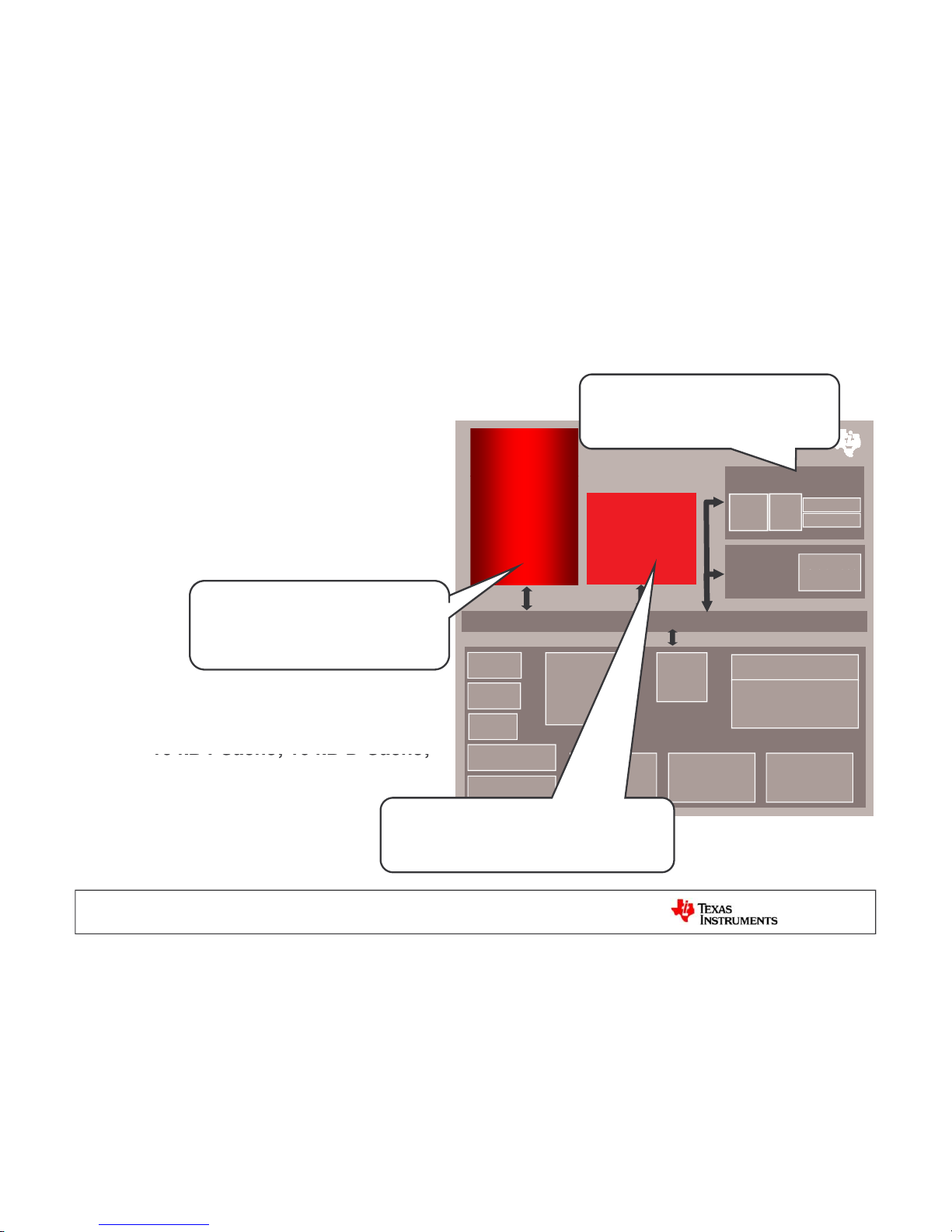
AM3517/05 Core and Accelerators
AM3517/05
processors
Cores
Multi window overlay system and
resizing for hardware accelerated
user interfaces
ARM
®
Cortex™-
A8
3D
Graphics
Accelerator
(3517)
Display Subsystem
10 bit DAC
10 bit DAC
LCD
Controller
Video
Enc
Video
Cores
600 MHz Cortex A-8 with NEON™
coprocessor
PowerVR SGX 3D graphics
Accelerator – up to 10M
L3/L4 Interconnect
16-bit Video
Input
Processing
Front End
polygons
/ second
Up to 1000 Dhrystone MIPS:
• OS’s like Linux or WinCE
• Excellent web experience
I2C x3
USB HS Host x2
Timers
GP x12
WDT x1
HDQ /
1-wire
USB OTG
w/PHY
EMAC
CAN
Memory
ARM:
MMC/SD/
SDIO x3
DDR2
GPMC
McBSP x5
UARTx3
+1 w/IrDA
McSPI x4
16 kBI-Cache; 16
kBD-
Cache;
256kB L2 Cache
On chip: 64kB SRAM; 128kB
ROM
DDR2 interface
• Up to 10M polygons per second
• Hardware based on screen display
GPMC: NAND/NOR I/F
•
Easily create robust GUI’s
7
Page 8
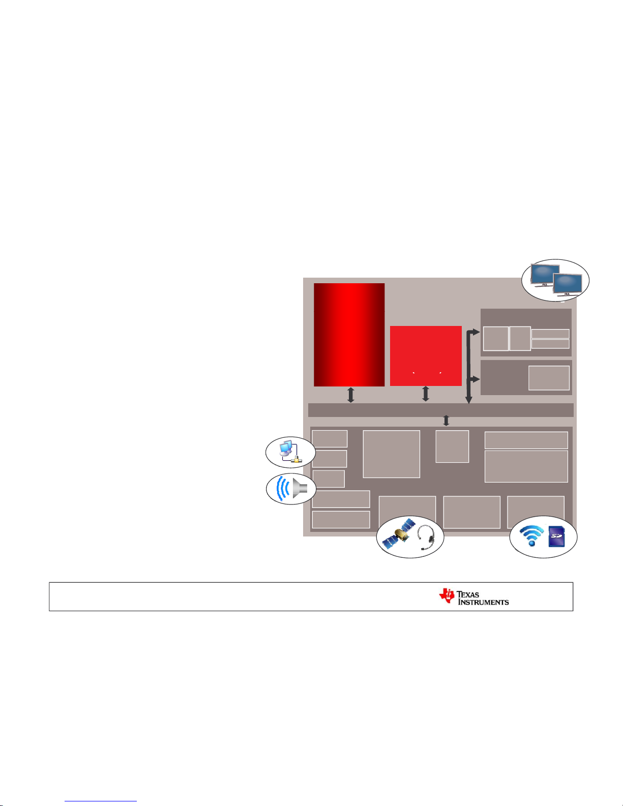
AM3517/05 Peripherals
AM3517/05
processors
Peripherals
CAN – High end controller area
network Controller (HECC)
USB 2.0 OTG w/PHY
ARM
®
Cortex™-
A8
3D
Graphics
Accelerator
(3517)
Display Subsystem
10 bit DAC
10 bit DAC
LCD
Controller
Video
Enc
Video
RMII EMAC controller 10/100
USB HS host x2
MMC/SD card interface x3
LCD controller and TV out
L3/L4 Interconnect
(3517)
16-bit Video
Input
Video
Processing
Front End
Display subsystem with PIP,
color space conversion, rotation,
resizing
1.8V or 3.3V IO
I2C x3
USB HS Host x2
Timers
GP x12
WDT x1
HDQ /
1-wire
USB OTG
w/PHY
EMAC
CAN
Power
Total Power: 0.5W – 1.5W
Standby Power: 12mW
MMC/SD/
SDIO x3
DDR2
GPMC
McBSP x5
UARTx3
+1 w/IrDA
McSPI x4
Package
ZCN – 17x17 mm, 0.65 mm pitch
Utilizes Via Channel™ Array
Technology with 0.8mm pitch
plus design rules.
ZER – 23x23 mm, 1.0mm pitch.
8
Page 9
AM3505/17 Platforms
Applications
Software
Compatibility
3D
Graphics
Compatibility
Shared
Peripheral
Set
AM3517
AM
™
ARM
Cortex-A8
600 MHz
Graphics
Open GL ES 2.0
Peripherals
AM
™
ARM
AM3505
Cortex
-
A8
600 MHz
Peripherals
9
Pin-for-pin compatible
Availability subject to applicable lead times
Page 10

CORTEX A-8 : Highlights
• First ARMv7 instruction-set architecture
• Superscalar architecture delivers high performance
–
Advanced dynamic Branch prediction
• 256 KB unified L2 cache
–
Dedicated, low
-
latency, high
-
BW interface to L1 cache
–
Dedicated, low
-
latency, high
-
BW interface to L1 cache
• Enhanced VFPv3
– Doubles number of double-precision registers
–
Adds new instructions to convert between fixed and floating point
• Efficient Run Time Compilation Target
–
Jazelle
-
RCT: Target for Java. Memory footprint reduced up to 3x
–
Jazelle
-
RCT: Target for Java. Memory footprint reduced up to 3x
• Trust Zone
– Normal & Secure worlds have different memory views
10
Page 11
AM35x Memory Controller
• Two dedicated memory
controllers/one
internal
memory
– SDRAM controller (EMIF4)
–
General purpose
memory
controller (GPMC)
– Internal memory (SRAM)
• On Chip Memory [SRAM-64 Kb]
•
Operates
at full L3
interconnect
(64bit@Core Clock /2)
11
Page 12
GPMC Controller
AM35x
Supported PsRAM, OneNAND,
• 16-bit external memory
controller
NOR/NAND Flash,
ASYNC Logic
1GB (128MB per CS-
•
GPMC can communicate with
many external devices:
– External asynchronous/synchronous 8-
Supported Size
(bits)
mux
mode)
16 KB (2 KB per CS
non-mux
mode)
bit wide memory/device
– External asynchronous/synchronous
16-bit wide memory/device
Max Clock
Speed
100 MHz
Chip Selects 8
–
External 16
-
bit non
-
multiplexed device
with limited address range (2 Kbytes)
– External 16-bit address/data-
Max Address
Space
2 KB non mux mode
128 MB mux mode
multiplexed NOR flash device
– External 8-bit/16-bit NAND flash
device
–
External 16
-
bit pseudo SRAM
12
Data Width
16 b
–
External 16
-
bit pseudo SRAM
(pSRAM) device
Page 13
DDR Controller
AM3517/05
SDRAM
mDDR/DDR2
• Supports mDDR / DDR2
•
DDR
controller has three
Supported
Measured
Throughput
810MB/sec
•
DDR
controller has three
functional blocks:
– Virtual Rotated Frame Buffer
(VRFB), supporting rotations of
Supported
Size (bits)
16M, 32M (2
Banks)
64M, 128M, 256M,
0
, 90
, 180
,270
– SDRAM memory-access
scheduler (SMS)
64M, 128M, 256M,
512M,1G,
2G (4 Banks)
Max Clock
166MHz
•
Optimizes latency and
bandwidth usage among
requestors
Speed
Chip Selects
2
Data Width
16/32b
–
SDRAM Controller
• Physical interface to DDR2 or
mDDR
13
Data Width
•
Two chip selects
Page 14

Power Management
•
AM35x power management features:
– Single voltage and power domain
– Multiple clock domains
–
Single Operating Voltage and Frequency
– Low power mode (standby)
•
Power, Reset and Clock Management (PRCM)
•
Power, Reset and Clock Management (PRCM)
module controls power management
• One voltage supply to device processors and
peripherals.
• Supports dynamic clock gating for power
management through clock domains.
–
A clock domain is a group of modules or subsections of device
that share a common clock
– By gating the clock to each domain, it is possible to cut a clock to
14
a group of inactive modules to lower their active power
consumption.
Page 15

AM35x Power Options
TPS65910
TPS650732
Touchscreen
Interface
RTC 32kHz
IntegratedIntegrated
Battery ChargerBattery Charger
AC & USB
w/ DPPM
1010--bit ADCbit ADC
4 inputs
Integration
TPS65023
3 DCDC
1x 5V Boost
3 DCDC
PowerPower
3 DCDC
2 LDO
DriversDrivers
25mA wLED
Driver
10mA LED
Driver
9 LDO
2 LDO
2 LDO
I2CI2C
InterfaceInterface
2 HS I2C
1 I2C
1 I2C
15
Page 16

AM35x development tools
AM3517
evaluation module
AM3517 eXperimenter
$995
$199
• AM3517
• PowerVR SGX
• Integrated processor, power
and
Wifi
module
• Includes Module and
interface board found on
AM3517EVM
•
Touch screen LCD
and
Wifi
module
• Touch screen LCD
• CAN, JTAG, Ethernet and
more via applications board
• Modular design
•
Touch screen LCD
available for purchase
separately
• Available only through
LogicPD
•
Linux and Windows
®
Embedded CE
LogicPD
16
Page 17

Getting Help
• TI E2E forums
– http://e2e.ti.com
• Embedded Processor Wiki page:
– http://wiki.omap.com/index.php/Main_Page
•
Self Serve Collateral
– http://ap-fpdsp-
swapps.dal.design.ti.com/index.php/Self_serve_collateral
• OMAP Developer Series Videos (5 Parts)
– http://focus.ti.com/docs/prod/folders/print/omap3530.html
(or on YouTube)
• Online Training www.ti.com/onlinetraining
17
Page 18

ARM-9
PRODUCT DETAILS
18
Page 19

Multiple peripheral, memory and performance
combinations
AM1707
AM1806
AM1808
AM1705
OS &
drivers
Example
code
PRU UART, PRU CAN, touch screen interface demos, etc
TI-provided Linux & Windows
®
Embedded CE
plus Developer Network offerings
ARM9
375 and 450 MHz
Memory
interface
SDRAM
SDRAM
DDR2/mDDR/
SDRAM
DDR2/mDDR/
SDRAM
Key
peripherals
EMAC
PRU
MMC/SD
USB 2.0
EMAC
PRU
USB 2.0
USB 1.1
LCD Ctr
PRU
USB 2.0
LCD Ctr
MMC/SD
EMAC
PRU
USB 2.0
USB 1.1
LCD Ctr
MMC/SD
MMC/SD
• Smart metering
Target
peripherals
• Intelligent
occupancy sensor
• Portable data terminal
• Point-of-service
• Educational consoles
• Industrial
automation
• Home automation
eQEP
eQEP
Video I/O
uPP
SATA
Video I/O
uPP
19
applications
•
Bar code scanner
Software Compatible
Page 20

AM1808/1806 microprocessors
Features
CPU Cores
– ARM926EJ-S™ (MPU) up to 450 MHz
Memory
ARM9
Subsystem
LCD
The boxes with yellow border are features
found in AM1808 and not in AM1806
High Speed
1024x1024
–
ARM:
– 16KB – L1 Program Cache
– 16KB – L1 Data Cache
– On-chip 128KB RAM
– mDDR, DDR2, SDRAM
ARM
926EJ-S
CPU
LCD
Controller
uPP
ADC FPGA, or
DSP Interface
LCD
Peripherals (1.8/ 3.3V IOs)
– 10/100 Ethernet MAC
– EMIFA - DDR (mDDR/DDR2)
– EMIFB – SDRAM/NAND Flash
– Video Port I/F – Video In/Out (BT.656)
– uPP and USB 2.0 OTG
CPU
Switched Central Resource (SCR) / EDMA
PRU
128KB
RAM
Video
IN/Out
–
SATA and USB 1.1 H/D (AM1808 only)
Power (1.0-1.2V Core, 1.8/3.3V IOs)
– Total Power < 182mW @ 300MHz, 1.2V, 25C
– Standby Power < 7mW @ 1.2V/ 25C
Peripherals
Connectivity
WD
(1)
System
HRPWM
UHPI
USB2.0
HS
USB
EMAC
SATA
eCAP/
PWM
High Speed
Package
– 13 x13mm nFBGA (0.65mm), 16x16mm BGA (0.8mm)
– Extended Temperature Grade Options
• Commercial (0C to 90C)
• Industrial (-40 to 90C)
• Extended (-40C to 105C)
Program/Data Storage
I2C
(2)
Serial Interfaces
Timer
(3)
(2)
UHPI
w/ PHY
UART
(3)
McASP
SPI
(2)
MMC/SD
(2)
1.1
EMAC
McBSP
(2)
Async/
SDRAM
EMIF
mDDR/
DDR2/
w/ PHY
(3)
Internet
– Pin to pin compatible processors:
• AM1808/AM1806/OMAP-L138
(2)
(3)
(2)
(2)
16-bit
16-bit
Bluetooth
Connectivity
20
Page 21

AM1707/1705 microprocessors
ARM9
Subsystem
The boxes with yellow border are features
found in AM1707 and not in AM1705
Features
CPU Cores
– ARM926EJ-S™ (MPU) up to 450 MHz
Memory
ARM
926EJ-S
CPU
– ARM:
– 16KB – L1 Program Cache
– 16KB – L1 Data Cache
– On-chip 128KB RAM
– SDRAM
1024x1024
LCD
CPU
Switched Central Resource (SCR) / EDMA
LCD
Controller
PRU
128KB
RAM
Peripherals (1.8/ 3.3V IOs)
– 10/100 Ethernet MAC
– EMIFA – Supports Async/NAND Flash (8/16-bit)
– EMIFB – Supports 133 MHz SDRAM (16/32-bit)
– USB 2.0 OTG
– USB 1.1 H/D (AM1707 only)
Peripherals
Connectivity
WD
(1)
System
HRPWM
USB2.0
USB
eCAP/
PWM
eQEP
EMAC
HPI
High Speed
Buttons and
Knobs
Power (1.0-1.2V Core, 1.8/3.3V IOs)
– Total Power < 270mW @ 300MHz, 1.2V, 70C
– Standby Power < 62mW @ 1.2V/ 25C
Program/Data Storage
I2C
(2)
Serial Interfaces
Timer
(2)
(3)
HS
UART
(3)
SPI
(2)
MMC/SD
(1)
1.1
McASP
(3)
EMIFB
SDRAM
32-bit
EMIFA
NAND/
SDRAM
(3)
(2)
EMAC
HPI
Internet
Package
– 17x17mm BGA (1.0mm) (AM1707 only)
– 26x26mm QFP (1.0mm), 176 Pins (AM1705 only)
– Extended Temperature Grade Options
• Commercial (0C to 90C)
• Industrial (-40 to 90C)
•
Extended (
-
40C to 105C)
(2)
(3)
(1)
(3)32-
bit
(BGA ONLY)
16-bit
Bluetooth
Connectivity
•
Extended (
-
40C to 105C)
• Automotive (-40C to 125C) (AM1707 only)
– Pin to pin compatible processors:
• AM1707/AM1705/OMAP-L137
21
Page 22

CPU Core – ARM926EJ-S
• 375/450 MHz
ARM926EJ-S
• Includes MMU
• 16K I-Cache
ARM926EJ-S
450 MHz
64K
Boot
ROM
8K
• 16K D-Cache
• 64K ROM
16K
I-Cache
16K
D-Cache
RAM
Vector
Table
MMU
• Boot ROM
• 8K RAM (Vector Table)
SCR
• ARM Interrupt Controller
• 32-inputs
128K RAM
(shared)
• Configurable Priority
22
Page 23

Universal Parallel Port (uPP AM18x only)
uPP Peripheral
High Speed parallel data port
What Is uPP?
Config
Registers
I/O
Channel
A
External Pins
CPU
Memory
Two
Bidirectional
and
Independent 16bit channels
Internal dedicated DMA to
streamline data I/O
I/O
Channel
B
Internal
DMA
External Pins
CPU
Interrupt
streamline data I/O
Simple I/O Protocol
Value of uPP
Configuration Throughput (MB/s)
1 Ch, 16-bit 120
2 Ch, 1 Way, 8
-
bit
120
Efficient Processor to FPGA
communication enabled by high
speed data I/O
2 Ch, 1 Way, 8
-
bit
120
2 Ch, 1 Way, 16-bit 160
2 Ch, 2 Way, 16-bit 240
Enable multi-processor system
design in various topologies
Interface with high speed ADCs
HPI (16
-
bit)
50
and DACs
23
Page 24

Programmable Real-time Unit (PRU)
1. What is PRU?
– Programmable Real-time Unit Subsystem
– Dual 32bit RISC processors running at ½ CPU freq.
– Local instruction and data RAM. Access to chip-level
resources
2. Why PRU?
–
Full programmability allows adding customer
differentiation
–
Efficient in performing embedded tasks that require
–
Efficient in performing embedded tasks that require
manipulation of packed memory mapped data
structures
–
Efficient in handling of system events that have tight
real-time constraints.
24
Page 25

PRU Value
1. Extend Connectivity and Peripheral capability
– Implement special peripherals and bus interfaces (e.g. UARTs)
–
Implement smart data movement schemes. Especially useful for
Audio algorithms (e.g. Reverb, Room Correction)
2.
Reduce System Power Consumption
– Allows switching off the ARM clocks
– Implement smart power controller by evaluating events before
waking up ARM. Maximized power
-
down time.
waking up ARM. Maximized power
-
down time.
3. Accelerate System Performance
–
Full programmability allows custom interface implementation
–
Full programmability allows custom interface implementation
– Specialized custom data handling to offload ARM for innovative
signal processing algorithm implementation
25
Page 26

PRU Subsystem
PRU Subsystem Functional Block Diagram
32 GPO
•
Provides two independent
programmable real-time (PRU)
cores
•
32-Bit Load/Store RISC
32-
bit Interconnect SCR
PRU0 Core
PRU1 Core
DRAM0
(512 Bytes)
DRAM1
(512 Bytes)
4KB IRAM
30 GPI
32 GPO
•
32-Bit Load/Store RISC
architecture
• 4K Byte instruction RAM (1K
instructions) per core
•
512 Bytes data RAM per core
bit Interconnect SCR
Master I/F
(to SCR2)
4KB IRAM
Interrupts to
30 GPI
•
512 Bytes data RAM per core
• PRU operation is little endian
• Includes Interrupt Controller for
system event handling
bit Interconnect SCR
Interrupt
Controller
(INTC)
Slave I/F
(from SCR2)
ARM INTC
Events from
Peripherals +
PRUs
•
I/O interface
• 30 input pins and 32 output
pins per PRU core (AM18x)
•
AM17x does not support PRU
AM17x does not support PRU
I/O
• Power management via single
power/sleep controller (PSC)
http://processors.wiki.ti.com/index.php/Programmable_Realtime_Unit_Subsystem
26
Page 27

AM1x development tools
AM18x
evaluation module
AM17x
evaluation module
Hawkboard
$1150
$845
$89
• Touch screen LCD
• Full peripheral access
•
Connector for PRU
• Supports AM18x, C674x,
or OMAP-L138 SOMs
• Touch screen LCD
• Community board for
OMAP-L138
•
Connector for PRU
daughter card
•
Full peripheral access
• Connector for PRU
daughter card
• Experimenter kit available
27
for $445
Order entry open
now!
Page 28

Sitara
Software
28
Page 29

It’s all about the software!
Sitara
™
AM35x MPUs
Innovative software – NRE and royalty-free
•
Full software development kit including:
– Base port to multiple industry leading Operating Systems
• Linux kernel 2.6.32 BSP
®
•
Windows
®
Embedded CE 6.0 BSP
– Full peripheral driver library
– Graphics demos
– Flashing, pad configuration, and PinMux utilities
• These are just a few of the many features TI provides to start
your application development
Active open source community and large ecosystem of developers:
29
Page 30

AM35x Software Stack
TI Base SW/Components
TI HW/Libraries
Applications Level Software
User interface
Browser/ media players
3rdparty/Customer
“Applications”
Board Support Package
Application frameworks – Java, Qt, GStreamer, Flash, Android, DShow, Direct Draw
Linux – Open Source - TI developed
Windows
®
Embedded CE– TI owned,
developed by MS gold partner
Video,
imaging,
speech,
audio
codecs
Android and Commercial Linux
–
Many
partners
RTOS – QNX, VxWorks, Nucleus, Integrity etc.
audio
codecs
and frameworks
(Cortex-
A8/Neon)
Accelerators
–
GFX
Peripherals
OS Kernel
Accelerators
–
GFX
AM35x
30
Page 31

It’s all about the software!
Sitara
™
AM1x MPUs
Innovative software – NRE- and royalty-free
•
Full software development kit including:
– Base port to multiple industry leading Operating Systems
• Linux kernel 2.6.33 BSP
•
Windows® Embedded CE BSP
– Full peripheral driver library
– Demos: PRU, touchscreen and more
– PRU configurable tool
• All this enables customers to rapidly develop and deploy their
products at competitive R&D costs
Active open source community and large ecosystem of developers:
31
Page 32

ARM9 Software Stack
TI Base SW/Components
TI HW/Libraries
Applications Level Software
User Interface
Browser/
Media Players
3rdparty/Customer
“Applications”
Media Players
Board Support Package
Application Frameworks – Java, Qt, GStreamer, Flash, Android, DShow, Direct Draw
Linux – Open Source - TI developed
Android – Open Source – TI Funded
WinCE Embedded – TI owned, Developed by MS gold partner
Commercial Linux and Android – Many partners
Video,
imaging,
Speech,
Audio Codecs and
frameworks
RTOS
–
QNX, VxWorks, Nucleus, Integrity etc.
(ARM9)
OS Kernel
ARM9 with on chip USB, Ethernet, SATA
Accelerators –PRU
AM18x and AM17x
32
Page 33

Commercial Linux Vendors
Vendor
Capabilities Supported Platforms
Linux build tool with support for
OMAP3530, DM355,
TimeSys
multiple kernel versions and
middleware packages that enables
users to easily customize distribution.
Lower cost than MV and WRS
OMAP
-
L137, DM6446,
OMAP-L138, AM 3517
Montavista
MVL Pro 4 and 5 are distributions
based on frozen version of Linux
kernel. MVL 6 is based on ‘GIT Linux’
released by TI. Customized
OMAP3530, DM355, DM365,
DM6446, DM6467,
OMAP-L137, OMAP-L138,
distributions (
mobilinux
, carrier grade)
targeted at vertical segments.
AM3517
Distributions based on frozen version
OMAP3530, DM355,
WindRiver
of Linux kernel. ‘Frozen’ kernel is
updated every two years to later
release. Customized distributions
targeted at vertical segments (mobile,
OMAP
-
L137,
OMAP
-
L138,
AM 3517
33
networking)
Page 34

Linux SW Dev Tool: CODESourcery
Sourcery G++
Complete software development environment based on the open-source Linux GNU Toolchain for ARM code
development with broad adoption in the Linux community.
Includes the GNU C and C++ compilers and run-time libraries, a source- and assembly-level debugger Debugger, the
Eclipse IDE, and many more tools designed for ARM platforms and Linux application development.
Important Note
Sourcery G++ will be included in EVM Kits by TI and
Link will be provided to Code Sourcery web site from TI.com; Customers to choose Sourcery G++ SW Edition of
choice.
Sourcery G++ Software Editions
Lite Personal Professional
30-day Installation Support No Yes Yes
Unlimited Support No No Yes
Priority Defect Correction No No Yes
Access to Updates, Knowledge Base No Yes Yes
Big Endian, Neon support No No Yes
GNU/Linux Application Simulator No Yes Yes
GNU C/C++ Compiler Yes Yes Yes
GNU Debugger (GDB) Yes Yes Yes
Eclipse IDE No Yes Yes
Annual Subscription Price per Host Free $399 $2799
–Professional Edition: Designed for enterprise software development; including Extra run-time libraries
34
–Personal Edition: Designed for individuals and small development teams; including access to updates and knowledge base
–Lite Edition: Free, command line-only tools
Page 35

More Linux Tool Support Options
More Linux Tool Support Options
Tool Debug Compile Other Features
and link
TI Code
Composer
Studio
Low Level DSP and
ARM
Low-level ARM (ARMv7) and
DSP (NEON roadmap)
Power Aware Debug
ARM Real View
Low Level ARM
Application
-
level ARM (ARMv7,
NEON)
http://www.arm.com/pro
ducts/DevTools/
Green Hills
Low Level and User
level ARM debug
and DSP
Low Level ARM
Trace
http://www.ghs.com/pro
ducts/arm_development.
html
Lauterbach
Low Level and User
level ARM debug
None Extensive Trace support
http://www.lauterbac
h.com/frames.html
35
and DSP
Page 36

3rd Party ARM Speech Codecs
Vendor
Speech Codecs
Audio Codecs
Ittiam
G.711 (E/D), G.726 (E/D), GSMAMR NB (E/D)
AAC-LC(E/D), AAC-HE(E/D), MP3(E/D),
BSAC(D), FLAC(D), OGG VORBIS (D),
WMA(E/D), Dolby-AC3 5.1(E/D), WMA-
Lossless (D),WMA
-
Pro LBR (D), MP2
-
5.1
(D),AAC-LC5.1 (E/D), WMA Pro 5.1 (E/D),
Enhance AAC+ 5.1 (E/D)
http://www.ittiam.com/pages/products/prod
ucts.htm
Ingenient
G.726(E/D), GSM-AMR WB+
(E/D)
AAC-LC(E/D), AAC-HE(E/D), MP3(E/D),
BSAC(D), FLAC(D), OGG VORBIS (D),
WMA(E/D), Dolby-AC3(E/D)
More Information:
http://www.ingenient.com/multimedia_com
pression.html
CouthIT
G.711 (E/D), G.722.1 (E/D),
G.723.1A (E/D), G.726 (E/D),
G.728 (E/D), G.729 AM (E/D),
GSM-AMR NB, WB and WB+
MP3 (D)
http://www.couthit.com/codecs.asp
36
(E/D), EVRC (E/D), ILBC (E/D)
Page 37

3rd parties ARM codec List
ARM Cortex A8 Video and Image Codecs
Vendor Video Codecs Image
Ittiam
DivX (D), H.263 Baseline (D), H.264
BP (E/D), H.264 MP (D), H.264 HP
(D), MPEG4 ASP (D), MPEG4 BP
JPEG (E/D)
(D), MPEG4 ASP (D), MPEG4 BP
(E/D), WMV9/VC1 BP/MP (D),
MPEG2 (on request)
H.263 Baseline (D), H.264 BP (D),
JPEG(E/D)
Visual ON
H.264 MP (D), MPEG4 SP/ASP (D),
DivX,/xVID (D), WMV
SP/MP(D),MPEG2 (D), SORENSON
(D), ON2 (D), Real (D)
Visual ON ALSO Support
http://www.visualon.com/english/Products/VisualO
nsoftwarecodecs.htm
Visual ON ALSO Support
Audio/Speech decoders: AAC, AMR,
WMA and MP3
37
Page 38

Windows® Embedded CE SW Strategy
Customers can obtain CE 6.0
Download BSP from TI
TI CE 6.0 BSP
Drivers, Application Framework, & Graphics Package
(Where ever applicable)
Does NOT include any 3P ARM -based codecs
Development Tools:
Visual Studio 2005 and Platform
Builder
Support: Partners for BSP (some Hours FREE BSP
support), Fee based Extended support.
For Graphics and Multimedia development - TI
Forums & Community
38
Forums & Community
Cost: BSP Download is Free*
Page 39

Windows Embedded CE System
Integrators / Consulting
Vendor Expertise/Services
TI Partner for BSP Development for OMAP35x. Supports system
BSQUARE
TI Partner for BSP Development for OMAP35x. Supports system
integration needs for customers. Specific solution are available for
SD/MMC, Adobe Flash etc.
US based embedded hardware and SW design company. Familiar with
Logic PD
TI devices. Working with many OMAP35x customers for WinCE system
integration.
WinCE training, application and driver development. Based in France.
Working with many OMAP35x for system integration around WinCE.
Adeneo
Have very good experience with mass market WinCE support (training
and enablement).
MPC Data
TI partner for WinCE BSP development for OMAP-L products. Have
good knowledge about TI products.
good knowledge about TI products.
Mistral
India-based embedded HW and SW design company. Familiar with TI
devices, WinCE, and TI multimedia stack components. Developed
WinCE
5.0 for TI on DM644x. Also developed WinCE 6.0 on DM644x and
39
Support.
Page 40

RTOS - Summary
•
Available for purchase from commercial suppliers
• Sales and Support is provided by the RTOS Supplier
•
TI works with RTOS supplier to enable their OS on TI platforms
Vendor OS Description Link
QNX Neutrino Micro kernel based operating
http://www.qnx.com/products/neutrino
•
TI works with RTOS supplier to enable their OS on TI platforms
system. Support for different
product segments.
_rtos/
Green Hills Integrity
Designed for reliability and
http://www.ghs.com/produ
VelOSity
security. Leader in security
applications.
cts.html
Wind River VxWorks Established RTOS vendor. Part
of Intel now.
http://www.windriver.com/
products/vxworks/
Mentor Gaphics Nucleus Nucleus is popular in wireless
handsets. Extending the same
to other markets also.
http://www.mentor.com/pr
oducts/embedded_softwa
re/
40
Express Logic
ThreadX
RTOS targeted at deeply
embedded applications
http://www.rtos.com/
Page 41

Why Sitara™ARM®microprocessors
• TI’s Sitara family offer various combinations of highperformance and low power levels
• Customers can reduce system risks and accelerate time to
market using standard and comprehensive HLOS Board
support packages and ARM-based software development tools
• TI is the largest ARM core licensee
supporting all major High Level
Operating Systems
41
Page 42

More Information
• AM35x landing page: www.ti.com/AM35x
•
Sitara
home page:
www.ti.com/sitara
• ARM home page: www.ti.com/arm
•
TI Embedded Processor Wiki:
wiki.davincidsp.com
• Forums: e2e.ti.com
•
Support:
support@ti.com
• Open Source Software Portal:
DesignSomething.org
• Training: www.ti.com/training
42
Page 43

THANK
YOU
 Loading...