

查询THS8134供应商
THS8134, THS8134A, THS8134B
TRIPLE 8-BIT, 80 MSPS VIDEO D/A CONVERTER
WITH TRI-LEVEL SYNC GENERATION
SLVS205D – MAY 1999 – REVISED MARCH 2000
features
D
Triple 8-Bit D/A Converters
D
Minimum 80 MSPS Operation
D
Direct Drive of Doubly-Terminated 75-Ω
Load Into Standard Video Levels
D
3×8 Bit 4:4:4, 2×8 Bit 4:2:2 or 1×8 Bit 4:2:2
(ITU-BT.656) Multiplexed YPbPr/GBR Input
Modes
D
Bi-Level (EIA) or Tri-Level (SMPTE) Sync
Generation With 7:3 Video/Sync Ratio
D
Integrated Insertion of Sync-On-Green/
Luminance or Sync-On-All Channels
D
Configurable Blanking Level
D
Internal Voltage Reference
applications
D
High-Definition Television (HDTV) Set-Top
Boxes/Receivers
D
High-Resolution Image Processing
D
Desktop Publishing
D
Direct Digital Synthesis/I-Q Modulation
See ALSO: THS8133 (10 bit, pin-compatible)
description
BPb7
BPb6
BPb5
BPb4
BPb3
BPb2
BPb1
BPb0
NC
NC
DV
DV
SS
DD
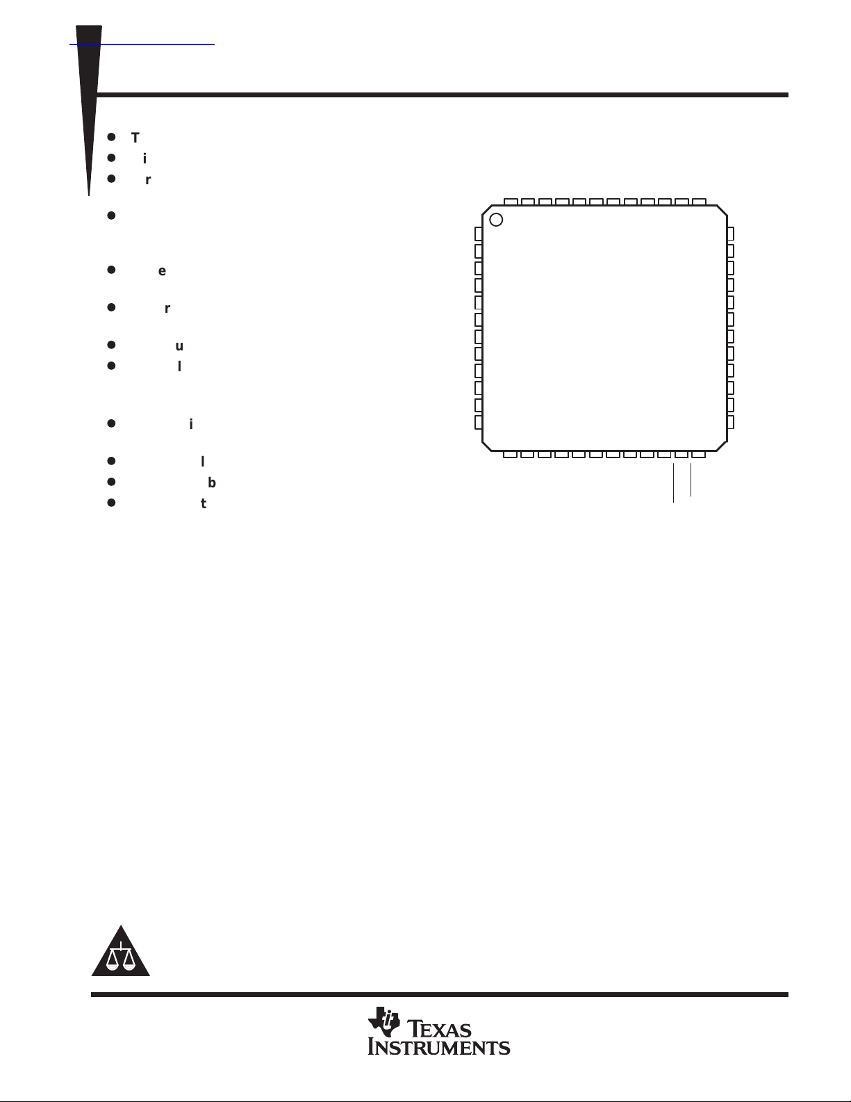
TQFP-48 PowerPAD PACKAGE
M2M1AV
47 46 45 44 4348 42
1
2
3
4
5
6
7
8
9
10
11
12
14 15
13
NC
NC
(TOP VIEW)
SS
ABPb
16
17 18 19 20
RPr1
RPr0
DD
AV
ARPr
RPr2
RPr3
SS
DD
AGYAVCOMP
AV
40 39 3841
22 23 24
21
RPr4
RPr5
RPr6
FSADJ
RPr7
BLANK
V
37
SYNC
REF
36
35
34
33
32
31
30
29
28
27
26
25
NC
NC
GY0
GY1
GY2
GY3
GY4
GY5
GY6
GY7
CLK
SYNC_T
The THS8134 is a general-purpose triple high-speed D/A converter (DAC) optimized for use in video/graphics
applications. The device operates from a 5-V analog supply and a 3-V to 5-V range digital supply . The THS8134
has a sampling rate up to 80 MSPS. The device consists of three 8-bit D/A converters and additional circuitry
for bi-level/tri-level sync and blanking level generation in video applications.
THS8134 is also well-suited in applications where multiple well-matched and synchronously operating DACs
are needed; for example, I-Q modulation and direct-digital synthesis in communications equipment.
The current-steering DACs can be directly terminated in resistive loads to produce voltage outputs. The device
provides a flexible configuration of maximum output current drive. Its output drivers are specifically designed
to produce standard video output levels when directly connected to a single-ended doubly-terminated 75 Ω
coaxial cable. Full-scale video/sync is generated in a 7:3 ratio, compliant with SMPTE standards for GBR and
YPbPr signals.
Furthermore, the THS8134 can generate both a traditional bi-level sync or a tri-level sync signal, as per the
SMPTE standards, via a digital control interface. The sync signal is inserted on one of the analog output
channels (sync-on-green/luminance) or on all output channels. Also, a blanking control signal sets the outputs
to defined levels during the nonactive video window.
The position of this defined (blanking) level and the temperature range, over which the maximum imbalance
between the inserted analog syncs (K
IMBAL(SYNC)
), are the only differences between the unrev , revA, and revB
device versions. Refer to the Available Options table.
Please be aware that an important notice concerning availability, standard warranty, and use in critical applications of
Texas Instruments semiconductor products and disclaimers thereto appears at the end of this data sheet.
PowerPAD is a trademark of Texas Instruments.
PRODUCTION DATA information is current as of publication date.
Products conform to specifications per the terms of Texas Instruments
standard warranty. Production processing does not necessarily include
testing of all parameters.
Copyright 2000, Texas Instruments Incorporated
POST OFFICE BOX 655303 • DALLAS, TEXAS 75265
1
THS8134, THS8134A, THS8134B
T
I/O
DESCRIPTION
TRIPLE 8-BIT, 80 MSPS VIDEO D/A CONVERTER
WITH TRI-LEVEL SYNC GENERATION
SLVS205D – MAY 1999 – REVISED MARCH 2000
description (continued)
Finally the input format can be either 3×8 bit 4:4:4, 2×8 bit 4:2:2, or 1×8 bit 4:2:2. This enables a direct interface
to a wide range of video DSP/ASICs including parts generating ITU-BT.656 formatted output data.
AVAILABLE OPTIONS
A
0°C to 70°C THS8134ACPHP
†
In the THS8134CPHP , the K
assured over full temperature range and the K
maximum specification is assured at 25°C. The position of
the blanking level is as shown in Table 1.
‡
In the THS8134ACPHP and the THS8134BCPHP, both the
K
maximum specification and the K
IMBAL
maximum specification are assured over the full temperature
range. The position of the blanking level is as shown in
Table 1.
IMBAL
PACKAGE
TQFP-48 PowerPAD
THS8134CPHP
THS8134BCPHP
maximum specification is
†
‡
‡
IMBAL(SYNC)
IMBAL(SYNC)
Terminal Functions
TERMINAL
NAME PIN
ABPb 45 O
AGY 41 O
ARPr 43 O
AV
DD
AV
SS
BLANK 23 I Blanking control input, active low. A rising edge on CLK latches BLANK. When asserted, the ARPr, AGY and
BPb0–BPb7 8–1 I Blue or Pb pixel data input bus. Index 0 denotes the least significant bit. Refer to functional description for
CLK 26 I Clock input. A rising edge on CLK latches RPr0-7, GY0-7, BPb0-7, BLANK, SYNC, and SYNC_T . The M2 input is
COMP 39 O Compensation terminal. A 0.1 µF capacitor must be connected between COMP and AVDD.
DV
DD
DV
SS
FSADJ 38 I Full-scale adjust control. The full-scale current drive on each of the output channels is determined by the value of
GY0–GY7 34–27 I Green or Y pixel data input bus. Index 0 denotes the least significant bit. Refer to functional description for
M1 47 I Operation mode control 1. M1 is directly interpreted by the device (it is not latched by CLK). M1 configures device
40,44 I Analog power supply (5 V ±10%). All AVDD terminals must be connected.
42,46 I Analog ground
12 I Digital power supply (3-V to 5-V range)
11 I Digital ground
Analog red, green and blue respectively Pr, Y and Pb current outputs, capable of directly driving a doubly
terminated 75-Ω coaxial cable.
ABPb outputs are driven to the blanking level, irrespective of the value on the data inputs. SYNC
precedence over BLANK,
different operating modes.
latched by a rising edge on CLK also, but only when additional conditions are satisfied, as explained in its
terminal description.
a resistor RFS connected between this terminal and AVSS. The nominal value of RFS is 430 Ω, corresponding to
26.67 mA full-scale current. The relationship between RFS and the full-scale current level for each operation
mode is explained in the functional description.
different operating modes.
according to Table 1.
so asserting SYNC (low) while BLANK is active (low) will result in sync generation.
takes
2
POST OFFICE BOX 655303 • DALLAS, TEXAS 75265
THS8134, THS8134A, THS8134B
I/O
DESCRIPTION
TRIPLE 8-BIT, 80 MSPS VIDEO D/A CONVERTER
WITH TRI-LEVEL SYNC GENERATION
SLVS205D – MAY 1999 – REVISED MARCH 2000
Terminal Functions (Continued)
TERMINAL
NAME PIN
M2 48 I Operation mode control 2. The second rising edge on CLK after a transition on SYNC latches M2. The
NC 9, 10,
RPr0–RPr7 15–22 I Red or Pr pixel data input bus. Index 0 denotes the least significant bit. Refer to functional description for different
SYNC 24 I Sync control input, active low. A rising edge on CLK latches SYNC. When asserted, only the AGY output
SYNC_T 25 I Sync tri-level control, active high. A rising edge on CLK latches SYNC_T . When asserted, a positive sync (higher
V
REF
13, 14,
35, 36
37 I/O Voltage reference for DACs. An internal voltage reference of nominally 1.35 V is provided, which requires an
interpretation is dependent on the polarity of the last SYNC
SYNC
L to H: latched as M2_INT
SYNC
T ogether with M1, M2_INT configures the device as shown in T able 1. When INS3_INT is high, the sync output is
inserted on all DAC outputs; a low will insert it only on the AGY output. See also Figure 2 and T able 2. The value of
M2 at power-up is undetermined. Therefore at least 1 L → H transition on SYNC
Not connected
operating modes.
(INS3_INT=L, see terminal M2) or ARPr, AGY and ABPb outputs (INS3_INT=H, see terminal M2) are driven to
the sync level, irrespective of the values on the data or BLANK
for the whole duration of sync, which is in the case of a tri-level sync both the negative and positive portion (see
Figure 7).
than blanking level) is generated when SYNC
is generated when SYNC
this signal positions the start of the positive transition. See Figure 6 for timing control.
The value on SYNC_T is ignored when SYNC
external 0.1 µF ceramic capacitor between V
by an externally supplied reference voltage.
H to L: latched as INS3_INT
is low. When generating a tri-level (negative-to-positive) sync, a L →H transition on
is low. When disabled, a negative sync (lower than blanking level)
is not asserted (high).
and AVSS. However, the internal reference can be overdriven
REF
transition:
is required to set M2.
inputs. Consequently, SYNC should remain low
POST OFFICE BOX 655303 • DALLAS, TEXAS 75265
3
THS8134, THS8134A, THS8134B
TRIPLE 8-BIT, 80 MSPS VIDEO D/A CONVERTER
WITH TRI-LEVEL SYNC GENERATION
SLVS205D – MAY 1999 – REVISED MARCH 2000
DV
DD
DV
SS
COMP V
Reference
FSADJ
REF
Bandgap
RPr[7:0]
GY[7:0]
BPb[7:0]
CLK
M1
M2
Input
Formatter
AVDDAV
R/Pr
Register
G/Y
Register
B/Pb
Register
Configuration
Control
SS
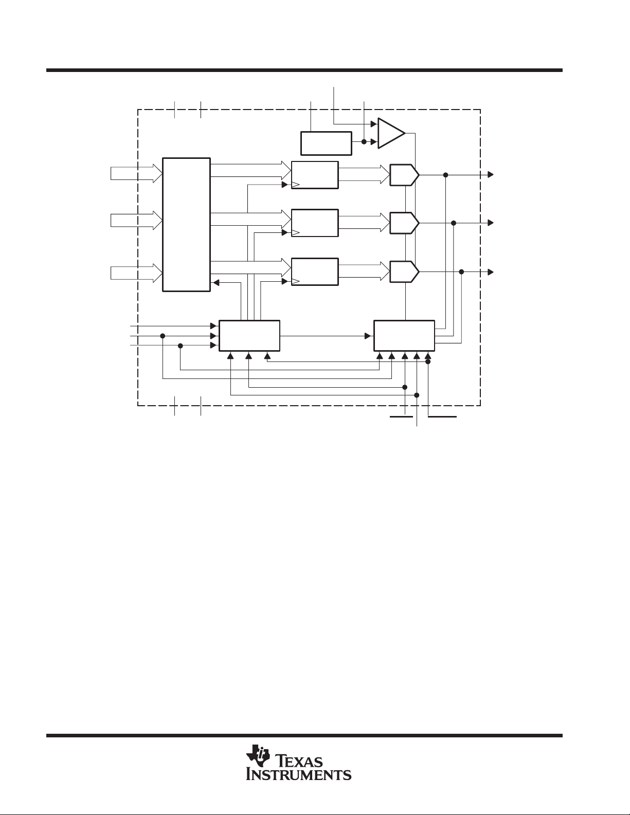
Figure 1. THS8134 Block Diagram
DAC
DAC
DAC
SYNC/BLANK
Control
SYNC
SYNC_T
ARPr
AGY
ABPb
BLANK
4
POST OFFICE BOX 655303 • DALLAS, TEXAS 75265
THS8134, THS8134A, THS8134B
TRIPLE 8-BIT, 80 MSPS VIDEO D/A CONVERTER
WITH TRI-LEVEL SYNC GENERATION
SLVS205D – MAY 1999 – REVISED MARCH 2000
functional description
device configuration
Input data to the device can be supplied from a 3x8b GBR/YPbPr input port. If the device is configured to take
data from all three channels, the data is clocked in at each rising edge of CLK. All three DACs operate at the
full clock speed of CLK.
In the case of 4:2:2 sampled data (for YPbPr) the device can be fed over either a 2x8 bit or 1x8 bit multiplexed
input port. An internal demultiplexer will route input samples to the appropriate DAC: Y at the rate of CLK, Pb
and Pr each at the rate of one-half CLK.
According to ITU-BT.656, the sample sequence is Pb-Y-Pr over a 1x8 bit interface (Y-port). The sample
sequence starts at the first rising edge of CLK after BLANK has been taken high (inactive). In this case the
frequency of CLK is two times the Y conversion speed and four times the conversion speed of both Pr and Pb.
With a 2x8 bit input interface, both the Y -port and the Pr-port are sampled on every CLK rising edge. The Pr-port
carries the sample sequence Pb-Pr. The sample sequence starts at the first rising edge of CLK after BLANK
has been taken high (inactive). In this case the frequency of CLK is equal to the conversion speed of Y and 2x
the conversion speed of both Pr and Pb.
The device’s operation mode is set by the M1 and M2 mode selection terminals, according to Table 1. The
operation mode also determines the blanking level, as explained below in the sync/blanking generation
sections.
Table 1. THS8134 Configuration
M1 M2_INT CONFIGURATION DESCRIPTION
L L GBR
3x8b–4:4:4
L H YPbPr
3x8b–4:4:4
H L YPbPr
2x8b–4:2:2
H H YPbPr
1x8b–4:2:2
NOTE 1: In all device versions, the blanking level on the AGY channel output corresponds to input code 0 of the DAC.
GBR mode 4:4:4. Data clocked in on each rising edge of CLK from G, B, and R input channels. For the
definition of the analog output levels during blanking, see note 1.
YPbPr mode 4:4:4. Data clocked in on each rising edge of CLK from Y , Pb and Pr input channels. For
the definition of the analog output levels during blanking, see note 1.
YPbPr mode 4:2:2 2x8 bit. Data clocked in on each rising edge of CLK from Y & Pr input channels. A
sample sequence of Pb–Pr–... should be applied to the Pr port. At the first rising edge of CLK after
BLANK
is taken high, Pb should be present on this port. For the definition of the analog output levels
during blanking, see note 1.
YPbPr mode 4:2:2 1x8 bit (ITU-BT .656 compliant). Data clocked in on each rising edge of CLK from Y
input channel. For the definition of the analog output levels during blanking, see note 1.
• In the THS8134CPHP and the THS8134ACPHP versions, the blanking level on the ABPb and ARPr channel outputs corresponds
to the 128 input code of the DAC, when sync is inserted on all three channels (INS3_INT=H), and to the 0 input code of the DAC,
when sync is only inserted on the Y channel (INS3_INT=L).
• In the THS8134BCPHP version, the blanking level on the ABPb and ARPr channel outputs corresponds to the 128 input code of
the DAC irrespective if sync is inserted on all three channels (INS3_INT=H), or if sync is inserted only on the Y channel
(INS3_INT=L).
POST OFFICE BOX 655303 • DALLAS, TEXAS 75265
5
THS8134, THS8134A, THS8134B
Apply to M2
TRIPLE 8-BIT, 80 MSPS VIDEO D/A CONVERTER
WITH TRI-LEVEL SYNC GENERATION
SLVS205D – MAY 1999 – REVISED MARCH 2000
Table 2. INS3_INT/M2_INT Selection on M2
LAST
EVENT ON
SYNC
H→L L or H X INS3_INT Sync insertion active: SYNC low enables sync generation on 1 (INS3_INT=L) or all 3
L→H X X M2_INT Device mode programming active: The DAC outputs reflect the DAC inputs
X = Don’t care
NOTE 2: M1 and M2 start configuring the device as soon as they are interpreted, which is continuously for M1 (static pin) or on the second rising
SYNC_T M1
edge on CLK after a transition on SYNC
M2
(see Note 2)
for M2. M2 is interpreted as either INS3_INT or M2_INT, as shown in Table 2.
DESCRIPTION
(INS3_INT=H) DAC outputs. SYNC_T determines the sync polarity.
(BLANK
=H) or are forced to the blanking level (BLANK=L). M2 is interpreted according
to Table 1.
programming example
Configuration of the device will normally be static in a given application. If M2_INT and INS3_INT need to be
both low or high, the M2 pin is simply tied low or high. If M2_INT and INS3_INT need to have different levels,
these can be easily derived from the signal on the SYNC pin, as shown in Table 3 and Figure 2.
Table 3. Generating M2 From SYNC
In order to have:
M2_INT INS3_INT
L H ...SYNC delayed by 2 CLK periods
H L ...inverted SYNC delayed by 2 CLK periods
:
The input formats and latencies are shown in Figures 3–5 for each operation mode.
if (M2 = SYNC_delayed) ⇒ M2_INT = L and INS3_INT = H)
if (M2 = NOT SYNC
_delayed) ⇒ M2_INT = H and INS3_INT = L)
Figure 2. Generating INS3_INT and M2_INT from M2
CLK
SYNC
M2
[=SYNC_delayed
INS3_INT
M2_INT
M2
[=NOT SYNC_delayed
INS3_INT
M2_INT
]
]
6
POST OFFICE BOX 655303 • DALLAS, TEXAS 75265
programming example (continued)
THS8134, THS8134A, THS8134B
TRIPLE 8-BIT, 80 MSPS VIDEO D/A CONVERTER
WITH TRI-LEVEL SYNC GENERATION
SLVS205D – MAY 1999 – REVISED MARCH 2000
CLK
RPr[7–0]
GY[7–0]
BPb[7–0]
BLANK
RPr[7–0]
T0 T1 T2 T3 T4 T5 T6 T7 T8
RPr(0) RPr(1) RPr(2) RPr(3) RPr(4) RPr(5) RPr(6) RPr(7) RPr(8)
GY(0) GY(1) GY(2) GY(3) GY(4) GY(5) GY(6) GY(7) GY(8)
BPb(0) BPb(1) BPb(2) BPb(3) BPb(4) BPb(5) BPb(6) BPb(7) BPb(8)
ARPr, AGY,
ABPb output
corresponding to RPr(0),
GY(0), BPb(0)
RPr(0), GY(0), BPb(0)
registered
data path latency = 7 CLK cycles
Figure 3. Input Format and Latency YPbPr 4:4:4 and GBR 4:4:4 Modes
T0 T1 T2 T3 T4 T5 T6 T7 T8
First registered sample on RPr[7–0] after L->H
on BLANK
Pb(0) Pr(0) Pb(2) Pr(2) Pb(4) Pr(4) Pb(6) Pr(6) Pb(8)
is interpreted as Pb[7–0]
T9
Pr(8)
GY[7–0]
BPb[7–0]
Y(0) Y(1) Y(2) Y(3) Y(4) Y(5) Y(6) Y(7) Y(8)
data path latency = 8 CLK cycles
Pb(0), Y(0)
registered
Pr(0), Y(1)
registered
Figure 4. Input Format and Latency YPbPr 4:2:2 2×8 bit Mode
Y(9)
ARPr, AGY,
ABPb output
corresponding to Pr(0),
Y(0), Pb(0)
POST OFFICE BOX 655303 • DALLAS, TEXAS 75265
7
THS8134, THS8134A, THS8134B
TRIPLE 8-BIT, 80 MSPS VIDEO D/A CONVERTER
WITH TRI-LEVEL SYNC GENERATION
SLVS205D – MAY 1999 – REVISED MARCH 2000
programming example (continued)
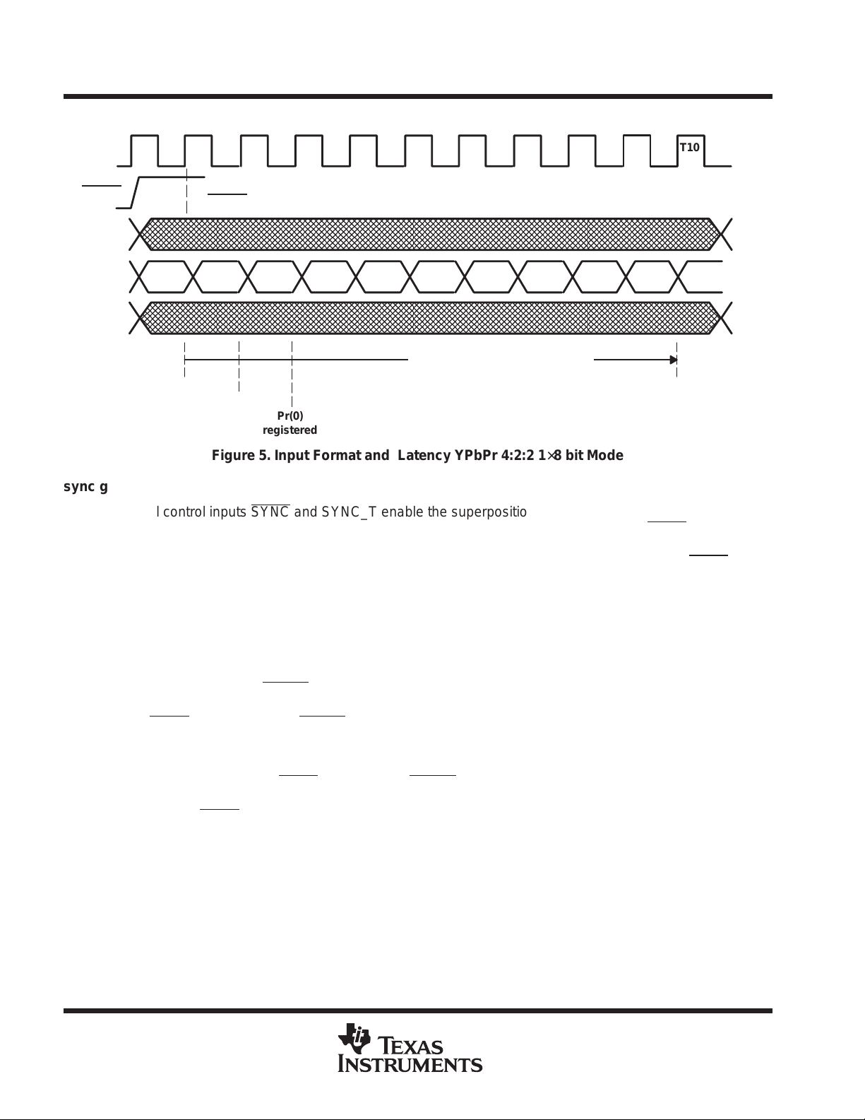
BLANK
RPr[7–0]
GY[7–0]
BPb[7–0]
T0 T1 T2 T3 T4 T5 T6 T7 T8
First registered sample on GYr[7–0] after L->H
on BLANK
Pb(0) Y(0) Pr(0) Y(2) Pb(4) Y(4) Pr(4) Y(6) Pb(8)
Pb(0)
registered
is interpreted as Pb[7–0]
Y(0)
registered
Pr(0)
registered
data path latency = 9 CLK cycles
T9
Y(8)
T10
Pr(8)
ARPr, AGY,
ABPb output
corresponding
to Pr(0),
Y(0), Pb(0)
Figure 5. Input Format and Latency YPbPr 4:2:2 1×8 bit Mode
sync generation
Additional control inputs SYNC
channel or on all three channels, depending on the setting of INS3_INT . By combining the SYNC
and SYNC_T enable the superposition of an additional current onto the AGY
and SYNC_T
control inputs, either bi-level negative going pulses or tri-level pulses can be generated. Depending on the timing
controls for these signals, both horizontal and vertical sync signals can be generated. Assertion of SYNC (active
low) will identify the sync period, while assertion of SYNC_T (active high) within this period will identify the
positive excursion of a tri-level sync.
Refer to the application information section for practical examples on the use of these control inputs for sync
generation.
blanking generation
An additional control input BLANK is provided that will fix the output amplitude on all channels to the blanking
level, irrespective of the value on the data input ports. However, sync generation has precedence over blanking;
that is, if SYNC is low , the level of BLANK is
don’t care
. The absolute amplitude of the blanking level with respect
to active video is determined by the GBR or YPbPr operation mode of the device. Refer to the application
information section for practical examples on the use of this control input for blank generation.
Figure 6 shows how to control SYNC, SYNC_T , and BLANK signals to generate tri-level sync levels and blanking
at the DAC output. A bi-level (negative) sync is generated similarly by avoiding the positive transition on
SYNC_T during SYNC low.
8
POST OFFICE BOX 655303 • DALLAS, TEXAS 75265
 Loading...